JP2005294530A - Organic semiconductor structure, manufacturing method thereof, and organic semiconductor device - Google Patents
Organic semiconductor structure, manufacturing method thereof, and organic semiconductor device Download PDFInfo
- Publication number
- JP2005294530A JP2005294530A JP2004107515A JP2004107515A JP2005294530A JP 2005294530 A JP2005294530 A JP 2005294530A JP 2004107515 A JP2004107515 A JP 2004107515A JP 2004107515 A JP2004107515 A JP 2004107515A JP 2005294530 A JP2005294530 A JP 2005294530A
- Authority
- JP
- Japan
- Prior art keywords
- organic semiconductor
- semiconductor layer
- region
- ring
- substrate
- Prior art date
- Legal status (The legal status is an assumption and is not a legal conclusion. Google has not performed a legal analysis and makes no representation as to the accuracy of the status listed.)
- Granted
Links
Images
Classifications
-
- H—ELECTRICITY
- H10—SEMICONDUCTOR DEVICES; ELECTRIC SOLID-STATE DEVICES NOT OTHERWISE PROVIDED FOR
- H10K—ORGANIC ELECTRIC SOLID-STATE DEVICES
- H10K85/00—Organic materials used in the body or electrodes of devices covered by this subclass
- H10K85/731—Liquid crystalline materials
-
- H—ELECTRICITY
- H10—SEMICONDUCTOR DEVICES; ELECTRIC SOLID-STATE DEVICES NOT OTHERWISE PROVIDED FOR
- H10K—ORGANIC ELECTRIC SOLID-STATE DEVICES
- H10K71/00—Manufacture or treatment specially adapted for the organic devices covered by this subclass
- H10K71/10—Deposition of organic active material
- H10K71/12—Deposition of organic active material using liquid deposition, e.g. spin coating
- H10K71/13—Deposition of organic active material using liquid deposition, e.g. spin coating using printing techniques, e.g. ink-jet printing or screen printing
-
- H—ELECTRICITY
- H10—SEMICONDUCTOR DEVICES; ELECTRIC SOLID-STATE DEVICES NOT OTHERWISE PROVIDED FOR
- H10K—ORGANIC ELECTRIC SOLID-STATE DEVICES
- H10K10/00—Organic devices specially adapted for rectifying, amplifying, oscillating or switching; Organic capacitors or resistors having potential barriers
- H10K10/40—Organic transistors
- H10K10/46—Field-effect transistors, e.g. organic thin-film transistors [OTFT]
- H10K10/462—Insulated gate field-effect transistors [IGFETs]
- H10K10/466—Lateral bottom-gate IGFETs comprising only a single gate
Landscapes
- Chemical & Material Sciences (AREA)
- Engineering & Computer Science (AREA)
- Crystallography & Structural Chemistry (AREA)
- Materials Engineering (AREA)
- Manufacturing & Machinery (AREA)
- Thin Film Transistor (AREA)
- Electroluminescent Light Sources (AREA)
- Liquid Deposition Of Substances Of Which Semiconductor Devices Are Composed (AREA)
Abstract
Description
本発明は、液晶性の有機半導体材料を用いて有機半導体層を形成してなる有機半導体構造物の製造方法、その製造方法により製造された有機半導体構造物及び有機半導体装置に関するものである。 The present invention relates to a method for manufacturing an organic semiconductor structure in which an organic semiconductor layer is formed using a liquid crystalline organic semiconductor material, an organic semiconductor structure manufactured by the manufacturing method, and an organic semiconductor device.
有機半導体装置の代表的なものとして、有機半導体を活性層(以下、有機半導体層という。)に利用した有機電界効果トランジスタ(有機FETともいう。)が挙げられる。有機FETは、薄膜大面積デバイスの実現のために、十分大きな面積において均一な電荷輸送特性と高い移動度を有することが求められている。 A typical example of an organic semiconductor device is an organic field effect transistor (also referred to as an organic FET) that uses an organic semiconductor as an active layer (hereinafter referred to as an organic semiconductor layer). Organic FETs are required to have uniform charge transport characteristics and high mobility in a sufficiently large area in order to realize a thin film large area device.
この有機FETにおいて、有機半導体層は、ペンタセンに代表される分子性結晶を真空製膜して形成されている。真空製膜による有機半導体層の形成方法では、製膜条件の最適化により、1cm2 /V・sを超える高い電荷移動度の有機半導体層が得られると報告されている(非特許文献1を参照)。
しかしながら、上述した真空製膜により形成された有機半導体層は、一般に、微結晶が集合した多結晶状態となって多くの粒界が存在し易い上、欠陥が生じ易く、そうした粒界や欠陥が電荷の輸送を阻害する。そのため、有機半導体層を真空製膜により形成する場合においては、有機半導体装置の構成素子である有機半導体層を、十分広い面積にわたって均一な性能で連続的に作ることは事実上困難であった。 However, the organic semiconductor layer formed by the above-described vacuum film formation is generally in a polycrystalline state in which microcrystals are aggregated and many grain boundaries are likely to exist, and defects are easily generated. Inhibits charge transport. Therefore, when the organic semiconductor layer is formed by vacuum film formation, it is practically difficult to continuously form the organic semiconductor layer, which is a constituent element of the organic semiconductor device, with a uniform performance over a sufficiently large area.
一方、高い電荷移動度を示す材料として、ディスコティック液晶が知られている(非特許文献2を参照)。しかしながら、このディスコティック液晶は、カラム状の分子配向に沿った一次元の電荷輸送機構に基づいて電荷の輸送が行われるので、厳密な分子配向の制御が要求され、工業的な利用が難しいという問題があった。このディスコティック液晶を有機半導体層の構成材料に使った薄膜トランジスタの成功例は、未だ報告されていない。 On the other hand, a discotic liquid crystal is known as a material exhibiting high charge mobility (see Non-Patent Document 2). However, since this discotic liquid crystal transports charges based on a one-dimensional charge transport mechanism along the columnar molecular orientation, strict control of molecular orientation is required, and industrial use is difficult. There was a problem. No successful example of a thin film transistor using this discotic liquid crystal as a constituent material of an organic semiconductor layer has been reported yet.
また、フェニルベンゾチアゾール誘導体等の棒状(ロッド状)の液晶性材料も、液晶状態で高い電荷移動度を示すことは既に報告されている(非特許文献2を参照)。しかしながら、棒状の液晶性材料を有機半導体層に利用した薄膜トランジスタの成功例は未だ報告されていない。なお、棒状の液晶性材料は、いくつかの液晶状態を有しているが、この液晶性材料の構造規則性が高くなるにつれて電荷の移動度は上昇する傾向にある。しかし、この液晶性材料がより構造規則性の高い結晶状態に転移すると、電荷の移動度が逆に低下ないし観測されず、当然、薄膜トランジスタの性能を発現することはなかった。 In addition, it has already been reported that rod-shaped liquid crystalline materials such as phenylbenzothiazole derivatives also exhibit high charge mobility in the liquid crystal state (see Non-Patent Document 2). However, no successful example of a thin film transistor using a rod-like liquid crystal material for an organic semiconductor layer has been reported yet. Note that the rod-like liquid crystalline material has several liquid crystal states, but the charge mobility tends to increase as the structural regularity of the liquid crystalline material increases. However, when the liquid crystalline material transitions to a crystalline state with higher structural regularity, the charge mobility is not reduced or observed, and naturally the performance of the thin film transistor is not exhibited.
また、分子分散系の高分子材料を有機半導体材料として使用する場合においては、この有機半導体材料を塗布することにより大面積にわたって均一な電荷輸送特性を有する有機半導体層を形成することができる。しかしながら、形成された有機半導体層は、電荷の移動度が10−5〜10−6cm2 /V・sと低く、しかも温度依存性や電場依存性があるという問題がある。 In the case where a molecular dispersion polymer material is used as the organic semiconductor material, an organic semiconductor layer having uniform charge transport characteristics over a large area can be formed by applying the organic semiconductor material. However, the formed organic semiconductor layer has a problem of low charge mobility of 10 −5 to 10 −6 cm 2 / V · s and temperature dependency and electric field dependency.
本発明は、上記の問題を解決したものであって、従来困難とされていた比較的大きな面積で均一で高い電荷輸送特性を持つ有機半導体構造物の製造方法、その製造方法により製造された有機半導体構造物及び有機半導体装置を提供するものである。 The present invention solves the above-described problems, and a method for producing an organic semiconductor structure having a uniform and high charge transport property in a relatively large area, which has been considered difficult, and an organic material produced by the method. A semiconductor structure and an organic semiconductor device are provided.
上記課題を解決する本発明の有機半導体構造物の製造方法は、基材上に液晶性有機半導体材料からなる有機半導体層を有する有機半導体構造物の製造方法であって、前記基材に撥油性領域及び当該撥油性領域で囲まれた親油性領域を形成する工程と、前記液晶性有機半導体材料及び溶媒を含む有機半導体層形成溶液を前記親油性領域に塗布する工程と、前記親油性領域に塗布された前記有機半導体層形成溶液中の前記溶媒を蒸発させて前記液晶性有機半導体材料を結晶化させる工程と、を有することを特徴とする。 The method for producing an organic semiconductor structure of the present invention that solves the above problems is a method for producing an organic semiconductor structure having an organic semiconductor layer made of a liquid crystalline organic semiconductor material on a substrate, and the substrate is oil repellent. A step of forming a lipophilic region surrounded by the region and the oil repellent region, a step of applying an organic semiconductor layer forming solution containing the liquid crystalline organic semiconductor material and a solvent to the lipophilic region, and the lipophilic region. And evaporating the solvent in the applied organic semiconductor layer forming solution to crystallize the liquid crystalline organic semiconductor material.
この発明によれば、液晶性有機半導体材料と溶媒を含む有機半導体層形成溶液を、撥油性領域で囲まれた親油性領域に塗布するので、塗布された溶液は、撥油性領域に流れ出し難く、その形状は液滴形状(半円弧状)となる。このような状態で塗布された溶液中の溶媒を蒸発させると、溶液濃度の高い部分である液滴表面から溶媒が蒸発して結晶化が開始するため、溶液と外部気相との接触面積が小さくなり、溶媒の蒸発速度と結晶化速度を非常に遅くすることができる。その結果、構造欠陥の少ない大きな結晶が得られ、大きな面積において均一化した電荷輸送特性を示す有機半導体層を形成することができる。また、この発明によれば、塗布された有機半導体層形成溶液は、撥油性領域には流れ出さずに親油性領域に形成されるので、あらかじめ設計された親油性領域パターンどおりの形状に有機半導体層を形成することができる。 According to this invention, since the organic semiconductor layer forming solution containing the liquid crystalline organic semiconductor material and the solvent is applied to the lipophilic region surrounded by the oil repellent region, the applied solution is difficult to flow out to the oil repellent region. The shape is a droplet shape (semi-arc shape). When the solvent in the solution applied in this state is evaporated, the solvent evaporates from the droplet surface, which is a portion with a high solution concentration, and crystallization starts, so that the contact area between the solution and the external gas phase is reduced. The solvent evaporation rate and crystallization rate can be made very slow. As a result, a large crystal with few structural defects can be obtained, and an organic semiconductor layer having uniform charge transport characteristics in a large area can be formed. Further, according to the present invention, the applied organic semiconductor layer forming solution is formed in the lipophilic region without flowing out to the oil repellent region, so that the organic semiconductor has a shape according to the previously designed lipophilic region pattern. A layer can be formed.
上記課題を解決するための本発明の有機半導体構造物は、基材上に、液晶性有機半導体材料からなる結晶相の有機半導体層が形成された有機半導体構造物であって、前記基材が撥油性領域と当該撥油性領域で囲まれた親油性領域とを有し、前記有機半導体層が前記親油性領域に形成されていることを特徴とする。 The organic semiconductor structure of the present invention for solving the above problems is an organic semiconductor structure in which an organic semiconductor layer having a crystalline phase made of a liquid crystalline organic semiconductor material is formed on a base material, and the base material is It has an oil-repellent region and a lipophilic region surrounded by the oil-repellent region, and the organic semiconductor layer is formed in the lipophilic region.
この発明によれば、基材の親油性領域に例えば溶液キャスト法(本願明細書では、基材に液晶性有機半導体材料の溶液を塗布し、その溶液に含まれる溶媒を蒸発させることによって製膜する方法をいう。)によって有機半導体層を製膜することができるので、構造欠陥の少ない大きな結晶を得易くなる。したがって、本発明の有機半導体構造物は、大きな面積において均一化した電荷輸送特性を有する有機半導体層を備えることができるので、薄膜大面積デバイスの実現に大きく寄与することができる。 According to the present invention, for example, a solution casting method (in the present specification, a liquid crystal organic semiconductor material solution is applied to a base material, and a solvent contained in the solution is evaporated to form a film on the lipophilic region of the base material. The organic semiconductor layer can be formed by the above-mentioned method, so that a large crystal with few structural defects can be easily obtained. Therefore, since the organic semiconductor structure of the present invention can be provided with an organic semiconductor layer having uniform charge transport characteristics in a large area, it can greatly contribute to the realization of a thin film large area device.
上述した本発明の有機半導体構造物においては、前記基材の前記有機半導体層が形成された面が配向処理されていることが好ましい。 In the organic semiconductor structure of the present invention described above, the surface of the base material on which the organic semiconductor layer is formed is preferably subjected to an orientation treatment.
この発明によれば、前記有機半導体層が、配向処理された基材上に形成されているので、液晶性分子を特定の向き又は方向に配向させることができる。 According to this invention, since the said organic-semiconductor layer is formed on the base material by which the alignment process was carried out, a liquid crystalline molecule can be aligned in a specific direction or direction.
上記課題を解決するための本発明の第1の形態に係る有機半導体装置は、少なくとも基板、ゲート電極、ゲート絶縁層、前記基板上に形成される液晶性有機半導体材料からなる結晶相の有機半導体層、ドレイン電極及びソース電極で構成される有機半導体装置であって、前記基板が撥油性領域及び当該撥油性領域で囲まれた親油性領域を有し、前記有機半導体層が前記親油性領域に形成されていることを特徴とする。 An organic semiconductor device according to a first aspect of the present invention for solving the above-described problem is an organic semiconductor having a crystalline phase comprising at least a substrate, a gate electrode, a gate insulating layer, and a liquid crystalline organic semiconductor material formed on the substrate. An organic semiconductor device including a layer, a drain electrode, and a source electrode, wherein the substrate has an oleophobic region and an oleophilic region surrounded by the oleophobic region, and the organic semiconductor layer is formed in the oleophilic region. It is formed.
上記課題を解決するための本発明の第2の形態に係る有機半導体装置は、少なくとも基板、ゲート電極、ゲート絶縁層、前記ゲート絶縁層に形成される液晶性有機半導体材料からなる結晶相の有機半導体層、ドレイン電極及びソース電極で構成される有機半導体装置であって、前記ゲート絶縁層が撥油性領域及び当該撥油性領域で囲まれた親油性領域とを有し、前記有機半導体層が前記親油性領域に形成されていることを特徴とする。 An organic semiconductor device according to a second embodiment of the present invention for solving the above-described problems is a crystalline organic material comprising at least a substrate, a gate electrode, a gate insulating layer, and a liquid crystalline organic semiconductor material formed on the gate insulating layer. An organic semiconductor device including a semiconductor layer, a drain electrode, and a source electrode, wherein the gate insulating layer has an oil-repellent region and an oleophilic region surrounded by the oil-repellent region, and the organic semiconductor layer It is formed in a lipophilic region.
これらの発明によれば、有機半導体層は、例えば溶液キャスト法により基板又はゲート絶縁層の親油性領域に形成することができるので、構造欠陥の少ない大きな結晶を得易くなる。したがって、本発明の第1及び第2の形態に係る有機半導体装置は、ドレイン電極及びソース電極間で均一化した電荷輸送特性を有する有機半導体層を備えることができるので、薄膜大面積デバイスの実現に大きく寄与することができる。 According to these inventions, since the organic semiconductor layer can be formed in the lipophilic region of the substrate or the gate insulating layer by, for example, a solution casting method, it becomes easy to obtain a large crystal with few structural defects. Therefore, the organic semiconductor device according to the first and second embodiments of the present invention can include an organic semiconductor layer having a uniform charge transport characteristic between the drain electrode and the source electrode, thereby realizing a thin film large area device. Can greatly contribute.
上述した本発明の有機半導体装置においては、前記液晶性有機半導体材料中の液晶性分子が、前記ゲート絶縁層上に形成された前記ドレイン電極と前記ソース電極との膜厚方向に並行に配向していることが好ましい。 In the organic semiconductor device of the present invention described above, the liquid crystalline molecules in the liquid crystalline organic semiconductor material are aligned in parallel in the film thickness direction of the drain electrode and the source electrode formed on the gate insulating layer. It is preferable.
上述した本発明の半導体装置においては、前記液晶性有機半導体材料中の液晶性分子が、前記ゲート絶縁層上に形成された前記ドレイン電極と前記ソース電極との膜厚方向に直交し、かつ、当該ドレイン電極と当該ソース電極との間に横列するように配向していることが好ましい。 In the semiconductor device of the present invention described above, the liquid crystalline molecules in the liquid crystalline organic semiconductor material are orthogonal to the film thickness direction of the drain electrode and the source electrode formed on the gate insulating layer, and It is preferably oriented so as to be arranged in a row between the drain electrode and the source electrode.
本発明の有機半導体構造物の製造方法によれば、構造欠陥の少ない大きな結晶からなる有機半導体層を形成することができるので、有機半導体層の電荷輸送特性を大きな面積において均一化させることができる。また、有機半導体層を、電子回路や有機半導体装置に応じてあらかじめ設計された親油性領域パターンに従った形状に形成することができる。加えて、有機半導体材料の溶液の塗布により有機半導体層を形成することが可能になるので、大きな面積において電荷輸送特性が均一化された有機半導体層を形成することが容易になる。 According to the method for producing an organic semiconductor structure of the present invention, an organic semiconductor layer made of a large crystal with few structural defects can be formed, so that the charge transport characteristics of the organic semiconductor layer can be made uniform over a large area. . Further, the organic semiconductor layer can be formed in a shape according to a lipophilic region pattern designed in advance according to an electronic circuit or an organic semiconductor device. In addition, since it is possible to form an organic semiconductor layer by applying a solution of an organic semiconductor material, it is easy to form an organic semiconductor layer with uniform charge transport characteristics over a large area.
本発明の有機半導体構造物及び有機半導体装置によれば、大きな面積において電荷輸送特性が均一化された有機半導体層を得易くなるので、薄膜大面積デバイスの実現に大きく寄与できる。 According to the organic semiconductor structure and the organic semiconductor device of the present invention, it is easy to obtain an organic semiconductor layer having uniform charge transport characteristics over a large area, and thus can greatly contribute to the realization of a thin film large area device.
以下、本発明を図面に基いて説明する。なお、これにより本発明が限定されるものではない。 Hereinafter, the present invention will be described with reference to the drawings. Note that the present invention is not limited thereby.
1. 有機半導体装置
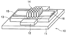
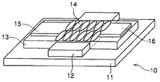
本発明の有機半導体装置10は、図1及び図2に示すように、少なくとも基板11、ゲート電極12、ゲート絶縁層13、液晶性有機半導体材料(以下、有機半導体材料という場合もある。)からなる結晶相の有機半導体層14、ドレイン電極15及びソース電極16で構成される。
1. Organic Semiconductor Device As shown in FIGS. 1 and 2, the
構成の一例としては、基板11上に、ゲート電極12、ゲート絶縁層13、液晶性有機半導体材料からなる結晶相の有機半導体層14、ドレイン電極15とソース電極16、保護膜(図示しない。)の順に構成される逆スタガー構造、又は、基板11上に、ゲート電極12、ゲート絶縁層13、ドレイン電極15とソース電極16、液晶性有機半導体材料からなる結晶状態の有機半導体層14、保護膜(図示しない。)の順に構成されるコプラナー構造、を挙げることができる。こうした構成からなる有機半導体装置10は、ゲート電極12に印加される電圧の極性に応じて、蓄積状態又は空乏状態の何れかで動作する。
As an example of the configuration, a
(基板)
基板11は、絶縁性の材料であれば広い範囲の材料から選択することができる。例えば、ガラス、アルミナ焼結体等の無機材料、ポリイミド膜、ポリエステル膜、ポリエチレン膜、ポリフェニレンスルフィド膜、ポリパラキシレン膜等の各種の絶縁性材料を挙げることができる。特に、高分子化合物からなる膜を用いると、軽量でフレシキブルな有機半導体装置を作製することができるので、極めて有用である。なお、本発明で適用される基板11の厚さは、25μm〜1.5mm程度である。
(substrate)
The
(ゲート電極)
ゲート電極12は、ポリアニリン、ポリチオフェン等の有機材料からなる電極又は導電性インキを塗布して形成した電極であることが好ましい。これらの電極は、有機材料や導電性インキを塗布して形成できるので、電極形成プロセスが極めて簡便となるという利点がある。塗布法の具体的な手法としては、スピンコート法、キャスト法、引き上げ法等が挙げられる。
(Gate electrode)
The
なお、既存のフォトリソグラフ法を用いて電極を形成してもよい。この場合には、金、白金、クロム、パラジウム、アルミニウム、インジウム、モリブデン、ニッケル等の金属、これら金属を用いた合金、ポリシリコン、アモリファスシリコン、錫酸化物、酸化インジウム、インジウム・錫酸化物(ITO)等の無機材料を、電極形成用の材料として挙げることができる。また、これらの材料を2種以上併用してもよい。 Note that the electrodes may be formed using an existing photolithographic method. In this case, metals such as gold, platinum, chromium, palladium, aluminum, indium, molybdenum, nickel, alloys using these metals, polysilicon, amorphous silicon, tin oxide, indium oxide, indium / tin oxide An inorganic material such as (ITO) can be used as the electrode forming material. Two or more of these materials may be used in combination.
ゲート電極の膜厚は、その材質の導電率によるが、50〜1000nm程度であることが好ましい。ゲート電極の厚さの下限は、電極材料の導電率及び下地基板との密着強度によって異なる。ゲート電極の厚さの上限は、後述のゲート絶縁層及びソース・ドレイン電極対を設けた際に、下地基板とゲート電極の段差部分におけるゲート絶縁層による絶縁被覆が十分で、かつその上に形成する電極パターンに断線を生ぜしめないことが必要である。特に、可とう性がある基板を使用した場合には、応力のバランスを考慮する必要がある。 The thickness of the gate electrode depends on the conductivity of the material, but is preferably about 50 to 1000 nm. The lower limit of the thickness of the gate electrode varies depending on the conductivity of the electrode material and the adhesion strength with the base substrate. The upper limit of the thickness of the gate electrode is that when a gate insulating layer and a source / drain electrode pair, which will be described later, are provided, the insulating coating by the gate insulating layer at the stepped portion of the base substrate and the gate electrode is sufficient and formed thereon It is necessary not to cause disconnection in the electrode pattern. In particular, when a flexible substrate is used, it is necessary to consider the balance of stress.
(ゲート絶縁層)
ゲート絶縁層13は、上記のゲート電極12と同じように、有機材料を塗布して形成したものであることが好ましく、使用される有機材料としては、ポリクロロピレン、ポリエチレンテレフタレート、ポリオキシメチレン、ポリビニルクロライド、ポリフッ化ビニリデン、シアノエチルプルラン、ポリメチルメタクリレート、ポリサルフォン、ポリカーボネート、ポリイミド、ポリビニルアルコール等を挙げることができる。塗布法の具体的な手法としては、スピンコート法、キャスト法、引き上げ法等が挙げられる。
(Gate insulation layer)
The
なお、CVD法等の既存パターンプロセスを用いてもよく、その場合には、SiO2 、SiNx、Al2 O3 等の無機材料が好ましく使用される。また、これらの材料を2種以上併用してもよい。 Incidentally, it may be used conventional pattern process such as CVD, in which case the, SiO 2, SiNx, inorganic material, such as Al 2 O 3 are preferably used. Two or more of these materials may be used in combination.
有機半導体装置の移動度は電界強度に依存するので、ゲート絶縁層の膜厚は、50〜200nm程度であることが好ましい。このときの絶縁耐圧は、2MV/cm以上であることが望ましい。 Since the mobility of the organic semiconductor device depends on the electric field strength, the thickness of the gate insulating layer is preferably about 50 to 200 nm. In this case, the withstand voltage is preferably 2 MV / cm or more.
(ドレイン電極及びソース電極)
ドレイン電極15及びソース電極16は、仕事関数の大きい金属で形成されることが好ましい。その理由としては、液晶性有機半導体材料は、電荷を輸送するキャリアがホールであることから、有機半導体層14とオーミック接触をとることが必要となるからである。ここでいう仕事関数とは、固体中の電子を外部に取り出すのに必要な電位差であり、真空準位とフェルミ準位のエネルギー差を電荷量で割った値として定義される。好ましい仕事関数としては、4.6〜5.2eV程度であり、具体的には、金、白金、透明導電膜(インジウム・スズ酸化物、インジウム・亜鉛酸化物等)等が挙げられる。透明導電膜は、スパッタリング法、電子ビーム(EB)蒸着法で形成することができる。なお、本発明で適用されるドレイン電極15及びソース電極16の厚さは、50〜100nm程度である。
(Drain electrode and source electrode)
The
(有機半導体層)
有機半導体層14は、液晶性有機半導体材料により形成された結晶相からなる層である。
(Organic semiconductor layer)
The
本発明に適用される有機半導体材料は、下記化学式1に示す液晶性分子からなる。
The organic semiconductor material applied to the present invention is composed of liquid crystalline molecules represented by the following
![]()
![]()
ここで、式中Aは、L個の6π電子系環、M個の8π電子系環、N個の10π電子系環、O個の12π電子系環、P個の14π電子系環、Q個の16π電子系環、R個の18π電子系環、S個の20π電子系環、T個の22π電子系環、U個の24π電子系環、V個の26π電子系環(但し、L,M,N,O,P,Q,R,S,T,U及びVは、それぞれ0〜12の整数を表し、L+M+N+O+P+Q+R+S+T+U+V=1〜12とする。)を含む骨格構造を有するコア部位を表す。また、式中B及びB’は、屈曲性の高い鎖状構造、又は、水素若しくはハロゲン等の官能基を表す。 In the formula, A is L 6π electron ring, M 8π electron ring, N 10π electron ring, O 12π electron ring, P 14π electron ring, Q 14π electron ring, Q pieces 16π electron ring, R 18π electron ring, S 20π electron ring, T 22π electron ring, U 24π electron ring, V 26π electron ring (provided that L, M, N, O, P, Q, R, S, T, U, and V each represents an integer of 0 to 12, and represents a core portion having a skeleton structure including L + M + N + O + P + Q + R + S + T + U + V = 1-12). In the formula, B and B ′ each represent a highly flexible chain structure or a functional group such as hydrogen or halogen.
上記化学式1に示す液晶性分子のAにおいて、6π電子系環としては、例えば、ベンゼン環、フラン環、チオフェン環、ピロール環、2H−ピラン環、4H−チオピラン環、ピリジン環、オキサゾール環、イソオキサゾール環、チアゾール環、イソチアゾール環、フラザン環、イミダゾール環、ピラゾール環、ピラジン環、ピリミジン環、ピリタジン環、トロボロン環を挙げることができ、8π電子系環としては、例えば、ペンタレン環、インデン環、インドリジン環、4H−キノリジン環を挙げることができ、10π電子系環としては、例えば、ナフタレン環、アズレン環、ベンゾフラン環、イソベンゾフラン環、1−ベンゾチオフェン環、2−ベンゾチオフェン環、インドール環、イソインドール環、2H−クロメン環、1H−2−ベンゾビラン環、キノリン環、イソキノリン環、1,8−ナフチリジン環、ベンゾイミダゾール環、1H−インダゾール環、ベンゾオキサゾール環、ベンゾチアゾール環、キノキサリン環、キナゾリン環、シンノリン環、プテリジン環、プリン環、フタラジン環を挙げることができ、12π電子系環としては、例えば、ヘプタレン環、ビフェニレン環、as―インダセン環、s−インダセン環、アナナフチレン環、フルオレン環、フェナレン環を挙げることができ、14π電子系環としては、例えば、フェナントレン環、アントラセン環、カルバゾール環、キサンテン環、アクリジン環、フェナントリジン環、ぺリミジン環、1,10−フェナントロリン環、フェナジン環、フェナルサジン環、テトラチアフルバレン環を挙げることができ、16π電子系環としては、例えば、フルオランテン環、アセフェナントリレン環、アセアントリレン環、ピレン環、チアントレン環、フェノキサチイン環、フェノキサジン環、フェノチアジン環を挙げることができ、18π電子系環としては、例えば、トリフェニレン環、クリセン環、ナフタセン環、プレイアデン環を挙げることができ、20π電子系環としては、例えば、ペリレン環を挙げることができ、22π電子系環としては、例えば、ビセン環、ペンタフェン環、ペンタセン環、を挙げることができ、24π電子系環としては、例えば、テトラフェニレン環、コロネン環、を挙げることができ、26π電子系環としては、例えば、ヘキサフェン環、ヘキサセン環、ルビセン環等を挙げることができる。
In the liquid crystal molecule A shown in the
本発明に適用される液晶性有機半導体材料には、上記化学式1に示した液晶性分子のうち、熱分解温度以下の温度において、少なくとも一種類の液晶状態を持つものが用いられる。「熱分解温度以下の温度において」とは、その材料がそれ自身分解されない状態を意味するものである。熱分解温度は、適用される材料により異なる。また、「少なくとも一種類の液晶状態を持つもの」とは、最低一種類の液晶状態を持つものが使用されるという意味である。例えば、後述するスメクティック液晶相(以下、Smともいう)においては、SmA相、SmB相、SmC相等の複数種類の液晶状態を有し、そのうちの少なくとも一種類の液晶状態を持つことである。そのような液晶性分子としては、上記化学式1中のAが下記化学式2〜36に示すような骨格構造を有する液晶性分子が挙げられる。
As the liquid crystalline organic semiconductor material applied to the present invention, those having at least one liquid crystal state at a temperature equal to or lower than the thermal decomposition temperature among the liquid crystalline molecules represented by the
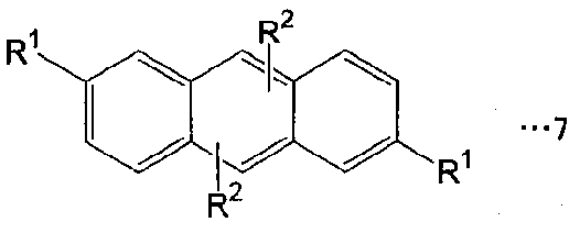
ここで、上記化学式2〜36中のR1は下記化学式37に示すような2価の構造を示し、別の骨格と連結する連結基を示す。これらの液晶性分子にR1が複数個ある場合には、それぞれが同一でもよいし、異なっていてもよい。また、これらの液晶性分子にR1はなくてもよい。上記化学式2〜36中のR2は下記化学式38に示すような官能基を示す。これらの液晶性分子にR2が複数個ある場合には、それぞれが同一でもよいし、異なっていてもよい。また、上記化学式2〜36中のXはCH又はNを示し、上記化学式2〜36中のYはS又はOを示す。 Here, R 1 in the chemical formulas 2 to 36 represents a divalent structure as shown in the following chemical formula 37, and represents a linking group linked to another skeleton. When there are a plurality of R 1 in these liquid crystalline molecules, each may be the same or different. Further, R 1 may not be present in these liquid crystalline molecules. R 2 in the chemical formulas 2 to 36 represents a functional group as shown in the following chemical formula 38. When there are a plurality of R 2 in these liquid crystalline molecules, each may be the same or different. X in the chemical formulas 2 to 36 represents CH or N, and Y in the chemical formulas 2 to 36 represents S or O.
上記化学式1のB及びB’は、屈曲性の高い鎖状構造、又は、水素若しくはハロゲン等の官能基である。屈曲性の高い鎖状構造は、基本的には直鎖状アルキル鎖又は分岐鎖状アルキル鎖であるが、このようなアルキル鎖には下記化学式37に示す39個の2価の構造の群から選択される構造が含まれていてもよい。また、屈曲性の高い鎖状構造は、下記化学式37に示す39個の2価の構造の群から選択された構造のみで構成されてもよく、この場合にはこの群から選択された1つの構造で構成されてもよいし、この群から選択された複数の構造が直鎖状又は分岐状に連結して構成されていてもよい。また、これらの屈曲性の高い鎖状構造は、置換基として下記化学式38に例示した21個の官能基の群から選択された官能基を有していてもよい。なお、上記化学式1中のB及びB’は、屈曲性の高い鎖状構造をとらない場合に、下記化学式38に例示した21個の官能基のいずれかとなる。
B and B ′ in the
但し、上記化学式38中のRは、炭素数1〜40の直鎖アルキル基又は分岐アルキル基を表す。 However, R in the said Chemical formula 38 represents a C1-C40 linear alkyl group or a branched alkyl group.
本発明に適用される有機半導体材料は、上述した液晶性分子からなる有機半導体材料のうち、この有機半導体材料と有機溶媒を含む有機半導体層形成溶液を、親油性領域パターン及び撥油性領域パターンが形成された基材に塗布して溶媒を蒸発させることにより結晶相とした場合に、大きな面積において構造欠陥の少ない結晶となるものが該当する。なお、本願明細書において「基材」とは、有機半導体層が形成される被形成部材をいい、具体的には、有機半導体装置を構成する基板11やゲート絶縁層13等である。
The organic semiconductor material applied to the present invention is an organic semiconductor layer-forming solution containing the organic semiconductor material and the organic solvent, and the oleophilic region pattern and the oil-repellent region pattern are the organic semiconductor materials composed of the liquid crystalline molecules described above. When a crystal phase is formed by applying the solution to the formed substrate and evaporating the solvent, this corresponds to a crystal having few structural defects in a large area. In the present specification, the “base material” refers to a member on which an organic semiconductor layer is formed, and specifically, the
本発明に適用される有機半導体材料の一例としては、例えば下記の化学式で示す化合物39,40を挙げることができる。 As an example of the organic semiconductor material applied to the present invention, for example, compounds 39 and 40 represented by the following chemical formulas can be mentioned.
上述した有機溶媒は、有機半導体材料の溶解度が、構造欠陥の少ない大きな結晶の成長が可能な程度に大きいものが好ましい。この有機溶媒は、使用する有機半導体材料の溶解度との関係から選択され、例えば、有機半導体材料に上記化学式39又は上記化学式40の化合物を使用するときは、キシレン、トルエン、ヘキサン、ブタノール、アセトン、クロロホルム等の有機溶媒を選択することができる。
The organic solvent described above preferably has a high solubility of the organic semiconductor material to such an extent that large crystals with few structural defects can be grown. This organic solvent is selected from the relationship with the solubility of the organic semiconductor material to be used. For example, when the compound of the
有機半導体材料と有機溶媒を含む有機半導体層形成溶液の濃度は、構造欠陥の少ない大きな結晶の成長が可能な程度の濃度であることが好ましく、使用する有機半導体材料や有機溶媒に応じて最適な濃度が選択される。 The concentration of the organic semiconductor layer-forming solution containing the organic semiconductor material and the organic solvent is preferably such a concentration that allows the growth of large crystals with few structural defects, and is optimal depending on the organic semiconductor material and organic solvent used. The concentration is selected.
本発明の有機半導体装置10において、有機半導体層は、親油性領域及び撥油性領域を有する基材(例えばゲート絶縁層13の表面等。)の親油性領域に形成されている。また、有機半導体層14が形成されている親油性領域は、少なくとも撥油性領域に囲まれている状態となっている。本願の明細書においては、「親油性領域及び撥油性領域を有する」とは、有機溶媒の濡れ性が互いに異なる領域を有することをいい、本発明の有機半導体装置10においては、親油性領域と撥油性領域が区別される程度に、有機溶媒の濡れ性に差があることが好ましい。親油性領域と撥油性領域が区別される程度に有機溶媒の濡れ性に差があれば、基材の親油性領域(濡れ性が大きい領域)に有機半導体層形成溶液を塗布したときに、その親油性領域を囲む撥油性領域(濡れ性が小さい領域)にその塗布溶液が流れ出し難くなり(後述の図3を参照。)、あらかじめ設計した親油性領域パターンどおりに有機半導体層14を形成させることができる。なお、この親油性領域パターンは、電子回路や半導体構造物に応じて設計される。
In the
基材への親油性領域及び撥油性領域の形成は、まず基材(例えば、ゲート絶縁層13等。)の全面をあらかじめアルカリ処理により撥油化し、シランカップリング剤等を塗布することによりアルキル鎖を化学吸着させて親油化処理する。その後、マスクパターン(親油化処理パターン)が形成されたマスクでマスクし、ポリスチレン等を含む溶剤を塗布することにより上記アルキル鎖を保護し、上記マスクをはずし、その後アルカリ処理することにより、撥油化したい領域のアルキル鎖を除去して撥油性領域とする。最後に、上記ポリスチレン等を溶かしてマスクしていない領域を親油性領域とすることにより、親油性領域及び撥油性領域を形成することができる。
The formation of the lipophilic region and the oil-repellent region on the base material is performed by first making the entire surface of the base material (for example, the
また、基材への親油性領域及び撥油性領域の形成は、表面処理を施すことによって有機溶媒の濡れ性が相対的に高い領域と相対的に低い領域を形成することが可能な樹脂を基材(例えば、ゲート絶縁層等。)上にスピンコート等の塗布手段や各種の印刷手段で塗布し、その後、その樹脂に所定の表面処理を施すことによっても行うことができる。この場合、有機溶媒の濡れ性が相対的に高い領域が親油性領域となり、有機溶媒の濡れ性が相対的に低い領域が撥油性領域となる。 In addition, the formation of the lipophilic region and the oil-repellent region on the base material is based on a resin that can form a region having a relatively high wettability and a region having a relatively low wettability by organic surface treatment. It can also be carried out by applying a material (for example, a gate insulating layer) by a coating means such as spin coating or various printing means, and then applying a predetermined surface treatment to the resin. In this case, a region where the wettability of the organic solvent is relatively high becomes a lipophilic region, and a region where the organic solvent has a relatively low wettability becomes the oil repellent region.
表面処理によって親油性領域と撥油性領域を形成することが可能な樹脂としては、例えば垂直配向膜形成用のポリイミド樹脂や、フッ素系シリコーン樹脂等の撥油性樹脂等を挙げることができる。 Examples of the resin capable of forming the lipophilic region and the oil-repellent region by the surface treatment include a polyimide resin for forming a vertical alignment film and an oil-repellent resin such as a fluorine-based silicone resin.
例えば、上記のポリイミド樹脂を用いた場合の表面処理方法としては、(i)ポリイミド樹脂を塗布した基材を、マスクパターン(撥油化処理パターン)が形成され光触媒層を有するマスクで露光することにより、露光された部分のみを親水化してここを撥油性領域とする方法、(ii)光触媒を含有するポリイミド樹脂を塗布した基材を、マスクパターン(撥油化処理パターン)が形成されたマスクで露光することにより、露光された部分のみを親水化してここを撥油性領域とする方法等を挙げることができる。フッ素系シリコーン樹脂等の撥油性樹脂を用いた場合においても、上記(i)又は(ii)の方法により表面処理を施すことができる。この場合、露光により親水化された領域が親油性領域となり、非露光領域が撥油性領域となる。いずれにしても、上記(i)又は(ii)の方法で使用される光触媒としては、酸化チタンや酸化亜鉛等の微粒子を用いることができる。 For example, as a surface treatment method using the above polyimide resin, (i) a substrate coated with a polyimide resin is exposed with a mask having a mask pattern (oil-repellent treatment pattern) and a photocatalyst layer. (Ii) A mask on which a mask pattern (oil-repellent treatment pattern) is formed on a substrate coated with a polyimide resin containing a photocatalyst. By exposing with, the method of making only the exposed part hydrophilic and making this an oil-repellent region etc. can be mentioned. Even when an oil-repellent resin such as a fluorine-based silicone resin is used, the surface treatment can be performed by the method (i) or (ii). In this case, the region hydrophilized by exposure becomes a lipophilic region, and the non-exposed region becomes an oil repellent region. In any case, fine particles such as titanium oxide and zinc oxide can be used as the photocatalyst used in the method (i) or (ii).
有機半導体層14は、上記の有機半導体層形成溶液を、親油性領域と撥油性領域を有する基材の親油性領域に塗布し、有機半導体層形成溶液中の溶媒を蒸発させることによって、液晶性有機半導体材料が結晶化されたものである。この有機半導体層14は、構造欠陥の少ない大きな結晶からなり、あらかじめ設計された親油性領域パターンに従って形成されている。この結晶の面積は、20mm2以上であり、例えばおよそ80mm2程度である。また、バルク中の構造欠陥密度及び基材との界面での構造欠陥密度は1013cm−3以下であり、例えばおよそ2×1012cm−3程度である。なお、有機半導体層14が形成される雰囲気の温度や圧力等は、使用する有機半導体材料や溶媒等に応じて、構造欠陥の少ない大きな結晶が成長するように制御される。このような温度や圧力は、蒸発速度すなわち結晶成長速度を決定する因子となる。
The
次に、構造欠陥の少ない大きな結晶からなる有機半導体層14が形成されるメカニズムについて考察する。
Next, the mechanism by which the
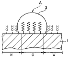
図3は、親油性領域パターン及び撥油性領域パターンが形成された基材の親油性領域に塗布された有機半導体層形成溶液の形状の一例を示す模式図であり、図4は、撥油性領域が形成されていない基材の親油性領域に塗布された有機半導体層形成溶液の形状の一例を示す模式図である。 FIG. 3 is a schematic diagram showing an example of the shape of the organic semiconductor layer forming solution applied to the lipophilic region of the base material on which the lipophilic region pattern and the oil repellent region pattern are formed. FIG. It is a schematic diagram which shows an example of the shape of the organic-semiconductor-layer formation solution apply | coated to the lipophilic area | region of the base material in which no is formed.
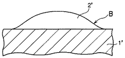
図3に示すように、基材1における撥油性領域Wに囲まれた親油性領域Oに塗布された有機半導体層形成溶液2は、液滴形状(半円弧状)となっている。このような状態でその溶媒を蒸発させると、溶液濃度の高い部分である液滴形状の上部(図3のA)から蒸発が始まって、結晶化が開始する。このとき、外部雰囲気の条件設定によって比較的少数の結晶核が液滴上部に生成し、これを核として溶液表面を覆うように結晶化が進む。そのため、溶液と外部気相との接触面積が小さくなり、その蒸発速度は非常に遅くなる。このようにして、溶媒の蒸発速度が遅くなることにより、有機半導体材料の結晶化速度が遅くなる。その結果、大面積において構造欠陥の少ない結晶からなる有機半導体層14が形成される。なお、このような疎水領域を有しない基材1’に有機半導体層形成溶液を塗布した場合には、図4に示すように、その有機半導体層形成溶液2’は流動し易いので平らでぬれの良い形状となり、溶媒の蒸発及び結晶化は有機半導体層形成溶液2’の裾部(図4のB。)から始まるため、このような結晶は得られない。
As shown in FIG. 3, the organic semiconductor layer forming solution 2 applied to the lipophilic region O surrounded by the oil repellent region W in the
有機半導体層14は、構造欠陥の少ない大きな結晶から形成されているので、キャリアが構造欠陥に捕捉され難く、大きな面積において均一な電荷輸送特性を示すという効果がある。また、この有機半導体層14は、電荷移動度が10−3〜10−1cm2/V・sという高い電荷輸送特性を示すという効果もある。例えば、化学式1に示す化合物を有機半導体材料とし、p−キシレンを有機溶媒に用いた場合の電荷移動度は、10−3〜10−2cm2/V・s以上となる。
Since the
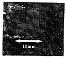
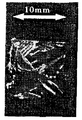
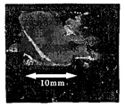
また、有機半導体層14は、電子回路や半導体装置に応じてあらかじめ設計された親油性領域パターンどおりの形状に形成できるという効果がある。この効果は液晶性の有機半導体材料のみに見られる。図5は、液晶性有機半導体材料(化学式1の化合物)を、基材の撥油性領域に囲まれた親油性領域に溶液キャスト法により製膜した場合の有機半導体層の偏光顕微鏡写真であり、図7は、液晶性でない有機半導体材料(アントラセン)を、基材の撥油性領域に囲まれた親油性領域に溶液キャスト法により製膜した場合の有機半導体層の偏光顕微鏡写真である。図5に示すように、液晶性有機半導体材料からなる有機半導体層は、親油性領域全面に形成されているが、図7に示すように、液晶性でない有機半導体材料からなる有機半導体層は、親油性領域全面ではなく一部に凝集した結晶となり、親油性領域パターンどおりの形状を有する有機半導体層は得られない。
Moreover, the
本発明の有機導体装置10においては、上述した有機半導体層14は、配向手段により特定の向き又は方向に配向した液晶性有機半導体材料により形成されていることが好ましい。配向処理されて結晶状態となった有機半導体層14は、従来知られている有機半導体層に比べても、クラックの発生等がなく、電荷輸送特性を均一にし、クラックに基づく電荷輸送速度の低下等の弊害が生じないという優れた効果を有している。
In the
液晶性分子の配向態様としては、(イ)図1に示すように、ゲート絶縁層13の上に形成されたドレイン電極15とソース電極16の膜厚方向に並行に配向している態様、又は、(ロ)図2に示すように、ゲート絶縁層13の上に形成されたドレイン電極15とソース電極16の膜厚方向に直交し、且つ、当該ドレイン電極15とソース電極16の間に横列するように配向している態様、等を挙げることができる。
As the orientation mode of the liquid crystalline molecules, (a) as shown in FIG. 1, the mode in which the
配向手段としては、有機半導体層14が形成される基材(例えば、ゲート絶縁層13の表面等。)に、液晶配向層を形成したり、ラビング処理等の配向処理をしたり、あるいは、配向処理を施した層と接触させたりする手段を挙げることができる。なお、この基材には、この配向処理のほかに上述した親油性領域及び撥油性領域を形成するための処理を行うが、これら処理はどちらを先に行ってもよい。
As an alignment means, a liquid crystal alignment layer is formed on a substrate (for example, the surface of the gate insulating layer 13) on which the
(層間絶縁層)
有機半導体装置10には、層間絶縁層を設けることが望ましい。層間絶縁層は、ゲート絶縁層13上にドレイン電極15及びソース電極16を形成する際に、ゲート電極12の表面の汚染を防ぐことを目的として形成される。したがって、層間絶縁層は、ドレイン電極15及びソース電極16を形成する前にゲート絶縁層13の上に形成される。そして、ソース電極15及びドレイン電極16が形成された後においては、チャネル領域上方に位置する部分を完全に除去又は一部を除去するように加工される。除去される層間絶縁層領域は、ゲート電極12のサイズと同等であることが望ましい。
(Interlayer insulation layer)
The
層間絶縁層を構成する材料としては、ケイ素酸化物、ケイ素窒化物、酸化アルミニウム等の無機材料や、ポリクロロピレン、ポリエチレンテレフタレート、ポリオキシメチレン、ポリビニルクロライド、ポリフッ化ビニリデン、シアノエチルプルラン、ポリメチルメタクリレート、ポリスルホン、ポリカーボネート、ポリイミド等の有機材料が挙げられる。 As the material constituting the interlayer insulating layer, inorganic materials such as silicon oxide, silicon nitride, aluminum oxide, polychloropyrene, polyethylene terephthalate, polyoxymethylene, polyvinyl chloride, polyvinylidene fluoride, cyanoethyl pullulan, polymethyl methacrylate, Examples thereof include organic materials such as polysulfone, polycarbonate, and polyimide.
(有機半導体装置)
本発明の有機半導体装置においては、構成1:基板/ゲート電極/ゲート絶縁層(液晶配向層を兼ねる。)/ソース・ドレイン電極/液晶性有機半導体層(/保護層)、構成2:基板/ゲート電極/ゲート絶縁層/ソース・ドレイン電極/液晶配向層/液晶性有機半導体層(/保護層)、構成3:基板/ゲート電極/ゲート絶縁層(液晶配向層を兼ねる。)/液晶性有機半導体層/ソース・ドレイン電極(パタニング)/保護層、構成4:基板/ソース・ドレイン電極/液晶性有機半導体層/ゲート絶縁層/ゲート電極/保護層兼基板、とすることもできる。
(Organic semiconductor device)
In the organic semiconductor device of the present invention, constitution 1: substrate / gate electrode / gate insulating layer (also serving as a liquid crystal alignment layer) / source / drain electrode / liquid crystalline organic semiconductor layer (/ protective layer), constitution 2: substrate / Gate electrode / gate insulating layer / source / drain electrode / liquid crystal alignment layer / liquid crystal organic semiconductor layer (/ protective layer), configuration 3: substrate / gate electrode / gate insulating layer (also serving as a liquid crystal alignment layer) / liquid crystal organic Semiconductor layer / source / drain electrode (patterning) / protective layer, constitution 4: substrate / source / drain electrode / liquid crystalline organic semiconductor layer / gate insulating layer / gate electrode / protective layer / substrate.
本発明の有機半導体装置では、構造欠陥の少ない大きな結晶から形成されている有機半導体層を形成し易いので、大きな面積において電荷輸送特性が均一で電荷移動度が高いという優れた効果を発揮する有機半導体装置を易くなる。 In the organic semiconductor device of the present invention, an organic semiconductor layer formed from a large crystal with few structural defects can be easily formed. Therefore, the organic semiconductor device exhibits excellent effects of uniform charge transport characteristics and high charge mobility in a large area. The semiconductor device becomes easy.
以下、本発明を実施例と比較例に基づいてさらに詳しく説明する。なお、本発明は下記の実施例に限定されるものではない。 Hereinafter, the present invention will be described in more detail based on examples and comparative examples. In addition, this invention is not limited to the following Example.
(実施例1)
有機半導体材料として、上記化学式39の化合物であるフェニルナフタレン誘導体(2−(4’−Pentylphenyl)−6−metyloxynaphthalene。以下、5−PNP−O1と略することがある。)を用いて、有機半導体装置を作製した。また、有機半導体材料としてこの材料を用いて、有機半導体層を作製し、各特性評価を行った。
(Example 1)
As an organic semiconductor material, a phenyl naphthalene derivative (2- (4′-Pentylphenyl) -6-methyloxynaphthalene, hereinafter may be abbreviated as 5-PNP-O1), which is a compound represented by Chemical Formula 39, is used as an organic semiconductor material. A device was made. In addition, using this material as an organic semiconductor material, an organic semiconductor layer was produced and evaluated for each characteristic.
(有機半導体装置の作製)
有機半導体材料として、上記の5−PNP−O1を用い、基板/ゲート電極/親油性領域パターン及び撥油性領域パターンが形成されたゲート絶縁層(液晶配向層を兼ねる。)/ソース・ドレイン電極/有機半導体層(/保護層)からなる実施例1の有機半導体装置を作製した。
(Production of organic semiconductor devices)
As the organic semiconductor material, the above-described 5-PNP-O1 is used, and a gate insulating layer (also serving as a liquid crystal alignment layer) on which a substrate / gate electrode / lipophilic region pattern and oleophobic region pattern are formed / source / drain electrode / An organic semiconductor device of Example 1 composed of an organic semiconductor layer (/ protective layer) was produced.
<基板>中性洗剤、純水、アセトン、IPAを順に用いて超音波洗浄したガラス基板(厚さ1.1mm、コーニング1737)を用いた。 <Substrate> A glass substrate (thickness 1.1 mm, Corning 1737) subjected to ultrasonic cleaning using neutral detergent, pure water, acetone, and IPA in this order was used.
<ゲート電極>ゲート電極は、上記の基板上に、Au(厚さ300nm)の短冊状パターン(電極幅100μm、電極間5mm)をメタルマスクを介して抵抗加熱蒸着して形成した。なお、同様の電極パターンとしては、ITO電極をウェットプロセスにてパタニングしても形成できる。 <Gate electrode> The gate electrode was formed on the above-mentioned substrate by resistance heating vapor deposition of a strip pattern (electrode width: 100 μm, electrode spacing: 5 mm) of Au (thickness: 300 nm) through a metal mask. A similar electrode pattern can also be formed by patterning an ITO electrode by a wet process.
<ゲート絶縁層>
(1)配向処理:
まず、ゲート絶縁層を形成し、これに配向処理を行った。
<Gate insulation layer>
(1) Orientation treatment:
First, a gate insulating layer was formed and subjected to orientation treatment.
(a)有機半導体材料の構成分子を基板面に並行に配向させた場合(図2を参照。);ゲート絶縁層として、感光性ポリイミド(東レ:UR−3140を10gとり、それをn−メチルピロリドン25gで希釈したもの。)をスピン塗布し、100℃にて乾燥後露光現像することによりゲート電極端子を露出させた。その後、最高温度350℃で焼成した後、膜厚300nmのゲート絶縁層を形成した。 (A) When the constituent molecules of the organic semiconductor material are aligned in parallel with the substrate surface (see FIG. 2); As a gate insulating layer, 10 g of photosensitive polyimide (Toray: UR-3140 is taken as n-methyl Spin-coated with 25 g of pyrrolidone), dried at 100 ° C., and exposed and developed to expose the gate electrode terminal. Thereafter, after baking at a maximum temperature of 350 ° C., a gate insulating layer having a thickness of 300 nm was formed.
こうして形成したポリイミド膜の表面をラビング(48mmのローラーに巻き付けたポリエステルをラビング布に用い、1200rpm、基板移動速度600mm/min)にて配向処理した。ラビング方向は、チャネル長方向(電荷輸送方向)に対して並行となる方向、直交する方向にてそれぞれ行った。 The surface of the polyimide film thus formed was subjected to an orientation treatment by rubbing (polyester wound around a 48 mm roller was used as a rubbing cloth, 1200 rpm, substrate moving speed 600 mm / min). The rubbing direction was performed in a direction parallel to the channel length direction (charge transport direction) and in a direction orthogonal thereto.
(b)液晶性有機半導体材料の構成分子を基板面に垂直(すなわち基板面と直角方向)に配向させた場合(図1を参照。); (B) When the constituent molecules of the liquid crystalline organic semiconductor material are aligned perpendicular to the substrate surface (that is, in a direction perpendicular to the substrate surface) (see FIG. 1);
RFスパッタ法にて上記ゲート電極を配した基板上に、SiO2 膜100nmを形成(出力100W×30分)した。この基板上で、本実施例で用いた液晶性有機半導体材料は垂直配向するので、TFTを構成した際の電荷は分子長軸に垂直な方向に輸送されるものが支配的となる。 An SiO 2 film having a thickness of 100 nm was formed (output: 100 W × 30 minutes) on the substrate on which the gate electrode was arranged by RF sputtering. Since the liquid crystalline organic semiconductor material used in this embodiment is vertically aligned on this substrate, the charge when the TFT is constructed is predominantly transported in the direction perpendicular to the molecular long axis.
(2)親油性領域パターン及び撥油性領域パターンの形成処理:
次に、配向処理したゲート絶縁層に、以下に示す親油性領域パターン及び撥油性領域パターンの形成処理をした。
(2) Lipophilic region pattern and oil repellent region pattern forming process:
Next, the formation treatment of the following lipophilic region pattern and oil repellent region pattern was performed on the gate insulating layer subjected to the alignment treatment.
配向処理したゲート絶縁層の全面に、炭酸ナトリウム溶液による超音波洗浄を20分間行って、ゲート絶縁層面全体を親水化した。次に、シランカップリング剤を塗布してから、120℃で2時間加熱することにより、ゲート絶縁層面全体にアルキル鎖を化学吸着させて疎水化した。その後、このゲート絶縁層面を、4mm×100μmの長方形のマスクパターンが形成されたマスクで、後に形成するソース・ドレイン電極間にチャネルが形成される配置となるようにマスクし、その上からポリスチレン(5wt%トルエン溶液)をスピンコート法により塗布して上記アルキル鎖を保護した後、上記マスクをはずし、5wt%水酸化ナトリウム水溶液に60分間浸すことにより、マスクされていた領域のアルキル鎖を除去して撥油性領域とした。最後に上記ポリスチレンをジクロロメチルで溶かしてマスクされていなかった領域を親油性領域とした。 The entire surface of the gate insulating layer subjected to the alignment treatment was subjected to ultrasonic cleaning with a sodium carbonate solution for 20 minutes to make the entire surface of the gate insulating layer hydrophilic. Next, the silane coupling agent was applied, and then heated at 120 ° C. for 2 hours, thereby chemically adsorbing alkyl chains on the entire surface of the gate insulating layer to make it hydrophobic. Thereafter, the gate insulating layer surface is masked with a mask in which a rectangular mask pattern of 4 mm × 100 μm is formed so that a channel is formed between source / drain electrodes to be formed later, and polystyrene ( 5 wt% toluene solution) is applied by spin coating to protect the alkyl chain, and then the mask is removed and the alkyl chain in the masked region is removed by immersing in a 5 wt% sodium hydroxide aqueous solution for 60 minutes. Thus, an oil-repellent region was obtained. Finally, an area that was not masked by dissolving the polystyrene with dichloromethyl was defined as a lipophilic area.
<ソース・ドレイン電極>
ソース・ドレイン電極パッド(チャネル長50μm、チャネル幅4mm)として、Ptを抵抗加熱蒸着にてメタルマスクを用いて形成した(電極厚さ20nm)。なお、ソース・ドレイン電極パッドからの引き出し電極線として、Alを用いた。
<Source / drain electrodes>
As source / drain electrode pads (channel length 50 μm,
<液晶性有機半導体層>
液晶性有機半導体材料として、5−PNP−O1を使用し、溶媒をp−キシレンとして1wt%の有機半導体層形成溶液を調製した。この有機半導体層形成溶液を、大気圧下雰囲気温度15℃にて、ゲート絶縁層上の親油性領域に滴下し、溶媒を約5時間かけて蒸発させることにより結晶を形成させて、厚さ400nmの有機半導体層を得た。
<Liquid crystal organic semiconductor layer>
As the liquid crystalline organic semiconductor material, 5-PNP-O1 was used, and a 1 wt% organic semiconductor layer forming solution was prepared using p-xylene as a solvent. This organic semiconductor layer forming solution is dropped into an oleophilic region on the gate insulating layer at an atmospheric temperature of 15 ° C. under atmospheric pressure, and a solvent is evaporated over about 5 hours to form a crystal having a thickness of 400 nm. An organic semiconductor layer was obtained.
(電荷移動度の評価)
有機半導体層の電荷輸送特性を評価するために、実施例1の有機半導体装置の電界効果移動度(層面に平行方向)の測定を行った。
(Evaluation of charge mobility)
In order to evaluate the charge transport characteristics of the organic semiconductor layer, the field effect mobility (in the direction parallel to the layer surface) of the organic semiconductor device of Example 1 was measured.
電荷輸送特性の評価を行うための実施例1の有機半導体装置は、液晶性有機半導体材料の構成分子を基板面に垂直に配向させた上記の有機半導体装置である(図1を参照。)。 An organic semiconductor device of Example 1 for evaluating charge transport characteristics is the above-described organic semiconductor device in which constituent molecules of a liquid crystalline organic semiconductor material are aligned perpendicular to the substrate surface (see FIG. 1).
この有機半導体装置について、ソース−ドレイン間電圧Vds:0〜−30V、ゲート電圧Vg:0〜−30Vの範囲で電圧を印加し、ソース−ドレイン間の電流Idsがゲート電圧Vgの印加によって変化する挙動を測定し、評価した。 In this organic semiconductor device, a voltage is applied in the range of the source-drain voltage Vds: 0 to −30 V and the gate voltage Vg: 0 to −30 V, and the current Ids between the source and drain changes depending on the application of the gate voltage Vg. The behavior was measured and evaluated.
その結果、電荷移動度として、10−3〜10−2cm2/V・sという高い数値が得られた。 As a result, a high numerical value of 10 −3 to 10 −2 cm 2 / V · s was obtained as the charge mobility.
(結晶状態の評価)
有機半導体層の結晶状態を評価するために、実施例1の有機半導体層について、偏光顕微鏡写真を観察した。
(Evaluation of crystal state)
In order to evaluate the crystal state of the organic semiconductor layer, a polarizing micrograph was observed for the organic semiconductor layer of Example 1.
この特性評価のための有機半導体層は、マスクパターンとして1cm×1cmの正方形パターンを用いて、上記の有機半導体装置の作製における親油性領域パターン及び撥油性領域パターンの形成処理と同様の処理をガラス基板上に施し、大気圧下、雰囲気温度10℃にて、このガラス基板上の親油性領域に5−PNP−O1の1wt%p−キシレン溶液を滴下し、溶媒を約7時間かけて蒸発させることによって作製した。 For the organic semiconductor layer for this characteristic evaluation, a 1 cm × 1 cm square pattern is used as a mask pattern, and a process similar to the formation process of the lipophilic region pattern and the oil repellent region pattern in the production of the organic semiconductor device described above is performed using glass. A 1 wt% p-xylene solution of 5-PNP-O1 is dropped into the lipophilic region on the glass substrate at atmospheric pressure and an atmospheric temperature of 10 ° C., and the solvent is evaporated over about 7 hours. It was prepared by.
この結晶状態の評価は、偏光顕微鏡(NIKON社製、型番OPTIPHOT2−POL)を用いて行った。 This crystal state was evaluated using a polarizing microscope (manufactured by NIKON, model number OPTIPHOT2-POL).
図5は、実施例1の有機半導体層の偏光顕微鏡写真である。この偏光顕微鏡写真の観察により、実施例1の有機半導体層は、透明度が高く、ミリメートルオーダーの面積の大きな結晶で形成されていることが分かった。 FIG. 5 is a polarization micrograph of the organic semiconductor layer of Example 1. From observation of this polarizing microscope photograph, it was found that the organic semiconductor layer of Example 1 was formed of crystals having high transparency and a large area on the order of millimeters.
(構造欠陥密度の評価)
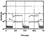
有機半導体層の構造欠陥密度を評価するために、実施例1の有機半導体層について、定常光電流の測定結果を考察した。
(Evaluation of structural defect density)
In order to evaluate the structural defect density of the organic semiconductor layer, the measurement result of the steady photocurrent was considered for the organic semiconductor layer of Example 1.
この特性評価のための有機半導体層は、くし型ITO電極(くし間L=30μm、くし幅W=10mm)が形成されたガラス基板に、マスクパターンとして4mm×100μmの長方形パターンを用いて、上記の有機半導体装置の作製における親油性領域パターン及び撥油性領域パターンの形成処理と同様の処理を施し、大気圧下、雰囲気温度10℃にて、このガラス基板上の親油性領域に5−PNP−O1の1wt%p−キシレン溶液を滴下し、溶媒を約7時間かけて蒸発させることによって作製した。 The organic semiconductor layer for this characteristic evaluation was formed by using a rectangular pattern of 4 mm × 100 μm as a mask pattern on a glass substrate on which comb-type ITO electrodes (comb spacing L = 30 μm, comb width W = 10 mm) were formed. The process similar to the formation process of the oleophilic region pattern and the oleophobic region pattern in the production of the organic semiconductor device is performed, and 5-PNP- is applied to the oleophilic region on the glass substrate at an atmospheric temperature of 10 ° C. under atmospheric pressure. It was prepared by dropping a 1 wt% p-xylene solution of O1 and evaporating the solvent over about 7 hours.
次に、それらの有機半導体層について、上記くし型ITO電極に定電圧をかけ、波長300〜400nmの光を当てて、光電流が時間の経過によって変化する挙動を評価した。 Next, with respect to these organic semiconductor layers, a constant voltage was applied to the comb-shaped ITO electrode, light having a wavelength of 300 to 400 nm was applied, and the behavior in which the photocurrent changed with time was evaluated.
図8のCは、実施例1の有機半導体層についての定常光電流測定結果である。この図より、光電流の立ち上がり立下りは急峻であることが分かる。このことから、実施例1の有機半導体層を形成する結晶は、構造欠陥が少ないものと考えられる。 C in FIG. 8 is a steady photocurrent measurement result for the organic semiconductor layer of Example 1. From this figure, it can be seen that the rise and fall of the photocurrent is steep. From this, it is considered that the crystal forming the organic semiconductor layer of Example 1 has few structural defects.
(結晶系の評価)
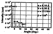
結晶状態の評価の際に用いた実施例1の有機半導体層について、X線回折装置(RIGAKU社製、型番;RAD−B)によって結晶構造の解析を行った。図9は、実施例1の有機半導体層のX線回折結果である。この結果より、実施例1の有機半導体層を形成する液晶性分子は、基材に対して垂直に立っていることが示唆された。実施例1の有機半導体層を形成する液晶がこのような結晶となる理由は、塗布された溶液中の液晶性有機半導体材料の液晶性分子が、基材上に垂直に形成された疎水基に沿って配向するためだと思われる。したがって、実施例1の有機半導体装置においては、配向処理を施さなくても、液晶性分子がドレイン電極とソース電極の膜厚方向に並行に配向して結晶化されているものと考えられる。
(Evaluation of crystal system)
About the organic-semiconductor layer of Example 1 used in the case of evaluation of a crystal state, the crystal structure was analyzed with the X-ray-diffraction apparatus (the RIGAKU company make, model number; RAD-B). FIG. 9 is an X-ray diffraction result of the organic semiconductor layer of Example 1. From this result, it was suggested that the liquid crystalline molecules forming the organic semiconductor layer of Example 1 were standing perpendicular to the substrate. The reason why the liquid crystal forming the organic semiconductor layer of Example 1 is such a crystal is that the liquid crystalline molecules of the liquid crystalline organic semiconductor material in the applied solution are formed on the hydrophobic groups formed vertically on the substrate. This is probably due to the orientation along Therefore, in the organic semiconductor device of Example 1, it is considered that the liquid crystal molecules are aligned and crystallized in parallel with the film thickness direction of the drain electrode and the source electrode without performing the alignment treatment.
(実施例2)
有機半導体材料として上記化学式40の化合物であるフェニルナフタレン誘導体(2−(4’−Octylphenyl)−6−dodecyloxynaphthalene。以下、8−PNP−O12と略することがある。)を用いた実施例2の有機半導体層について、実施例1と同様の各特性評価を行った。
(Example 2)
Example 2 in which a phenylnaphthalene derivative (2- (4′-Octylphenyl) -6-deoxyxynaphthalene, hereinafter may be abbreviated as 8-PNP-O12), which is a compound of
電荷移動度の評価及び構造欠陥密度の評価のための有機半導体層は、くし型Au電極(くし間L=200μm、くし幅W=28mm)が形成されたガラス基板に、マスクパターンとして4mm×100μmの長方形パターンを用いて、上記実施例1の有機半導体装置の作製における親油性領域パターン及び撥油性領域パターンの形成処理と同様の処理を施し、大気圧下雰囲気温度10℃にて、このガラス基板上の親油性領域に8−PNP−O12の1wt%p−キシレン溶液を滴下し、溶媒を約7時間かけて蒸発させることによって作製した。 The organic semiconductor layer for evaluation of charge mobility and structural defect density is 4 mm × 100 μm as a mask pattern on a glass substrate on which comb-type Au electrodes (comb spacing L = 200 μm, comb width W = 28 mm) are formed. Using this rectangular pattern, the glass substrate was subjected to the same treatment as the lipophilic region pattern and the oil-repellent region pattern in the production of the organic semiconductor device of Example 1, and the atmospheric temperature was 10 ° C. It was prepared by dropping a 1 wt% p-xylene solution of 8-PNP-O12 in the upper lipophilic region and evaporating the solvent over about 7 hours.
結晶状態の評価及び結晶系の評価のための有機半導体層は、マスクパターンとして1cm×1cmの正方形パターンを用いて、上記実施例1の有機半導体装置の作製における親油性領域パターン及び撥油性領域パターンの形成処理と同様の処理をガラス基板上に施し、大気圧下、雰囲気温度10℃にて、このガラス基板上の親油性領域に8−PNP−O12の1wt%p−キシレン溶液を滴下し、溶媒を約7時間かけて蒸発させることによって作製した。 The organic semiconductor layer for the evaluation of the crystal state and the evaluation of the crystal system uses a 1 cm × 1 cm square pattern as a mask pattern, and the lipophilic region pattern and the oil repellent region pattern in the production of the organic semiconductor device of Example 1 above. The glass substrate is subjected to the same treatment as the forming treatment, and a 1 wt% p-xylene solution of 8-PNP-O12 is dropped into the lipophilic region on the glass substrate at atmospheric pressure and an atmospheric temperature of 10 ° C. Made by evaporating the solvent over about 7 hours.
各特性評価の結果を以下に示す。 The results of each characteristic evaluation are shown below.
電荷移動度の評価において、電圧印加に伴い非線形電流成分が増加してトラップフリーの空間電荷制限電流が観測される領域での電荷移動度は、3×10⁻³cm2/V・sという高い値であった。 In the evaluation of charge mobility, the charge mobility in a region where a nonlinear current component increases with application of voltage and a trap-free space charge limited current is observed is as high as 3 × 10 −3 cm 2 / V · s. Value.
結晶状態の評価において、実施例2の有機半導体層は、図6に示すように、透明度が高く、ミリメートルオーダーの面積の大きな結晶で形成されていることが分かった。 In the evaluation of the crystal state, the organic semiconductor layer of Example 2 was found to be formed of crystals with high transparency and a large area on the order of millimeters, as shown in FIG.
構造欠陥密度の評価において、実施例2の有機半導体層の定常光電流は、図8のDに示すように、立ち上がり立下りが急峻であることが分かった。このことから、実施例2の有機半導体層を形成する結晶は、構造欠陥が少ないものと考えられる。 In the evaluation of the structural defect density, it was found that the steady photocurrent of the organic semiconductor layer of Example 2 has a steep rise and fall as shown in D of FIG. From this, it is considered that the crystal forming the organic semiconductor layer of Example 2 has few structural defects.
結晶系の評価において、実施例2の有機半導体層を形成する液晶性分子は、図10により、実施例1の場合と同様、基材に対して垂直に立っていることが示唆された。したがって、実施例2の有機半導体装置においても、配向処理を施さなくても、液晶性分子がドレイン電極とソース電極の膜厚方向に並行に配向して結晶化されるものと考えられる。 In the evaluation of the crystal system, it was suggested from FIG. 10 that the liquid crystalline molecules forming the organic semiconductor layer of Example 2 were standing perpendicular to the substrate as in Example 1. Therefore, even in the organic semiconductor device of Example 2, it is considered that the liquid crystalline molecules are aligned and crystallized in parallel with the film thickness direction of the drain electrode and the source electrode without performing the alignment treatment.
1 基材
2 有機半導体層形成溶液
10 有機半導体装置
11 基板
12 ゲート電極
13 ゲート絶縁層
14 有機半導体層
15 ドレイン電極
16 ソース電極
DESCRIPTION OF
Claims (7)
前記基材に撥油性領域及び当該撥油性領域で囲まれた親油性領域を形成する工程と、前記液晶性有機半導体材料及び溶媒を含む有機半導体層形成溶液を前記親油性領域に塗布する工程と、前記親油性領域に塗布された前記有機半導体層形成溶液中の前記溶媒を蒸発させて前記液晶性有機半導体材料を結晶化させる工程と、を有することを特徴とする有機半導体構造物の製造方法。 A method for producing an organic semiconductor structure having an organic semiconductor layer made of a liquid crystalline organic semiconductor material on a substrate,
Forming an oil-repellent region and an oleophilic region surrounded by the oil-repellent region on the substrate; and applying an organic semiconductor layer forming solution containing the liquid crystalline organic semiconductor material and a solvent to the lipophilic region. And evaporating the solvent in the organic semiconductor layer forming solution applied to the lipophilic region to crystallize the liquid crystalline organic semiconductor material. .
前記基材が撥油性領域と当該撥油性領域で囲まれた親油性領域とを有し、前記有機半導体層が前記親油性領域に形成されていることを特徴とする有機半導体構造物。 An organic semiconductor structure in which a crystalline organic semiconductor layer made of a liquid crystalline organic semiconductor material is formed on a substrate,
The organic semiconductor structure, wherein the substrate has an oil-repellent region and a lipophilic region surrounded by the oil-repellent region, and the organic semiconductor layer is formed in the lipophilic region.
前記基板が撥油性領域及び当該撥油性領域で囲まれた親油性領域を有し、前記有機半導体層が前記親油性領域に形成されていることを特徴とする有機半導体装置。 An organic semiconductor device comprising at least a substrate, a gate electrode, a gate insulating layer, a crystalline organic semiconductor layer made of a liquid crystalline organic semiconductor material formed on the substrate, a drain electrode, and a source electrode;
An organic semiconductor device, wherein the substrate has an oil-repellent region and a lipophilic region surrounded by the oil-repellent region, and the organic semiconductor layer is formed in the lipophilic region.
前記ゲート絶縁層が撥油性領域及び当該撥油性領域で囲まれた親油性領域とを有し、前記有機半導体層が前記親油性領域に形成されていることを特徴とする有機半導体装置。 An organic semiconductor device comprising at least a substrate, a gate electrode, a gate insulating layer, a crystalline organic semiconductor layer formed of a liquid crystalline organic semiconductor material formed on the gate insulating layer, a drain electrode, and a source electrode;
The organic semiconductor device, wherein the gate insulating layer has an oil-repellent region and a lipophilic region surrounded by the oil-repellent region, and the organic semiconductor layer is formed in the lipophilic region.
Priority Applications (2)
| Application Number | Priority Date | Filing Date | Title |
|---|---|---|---|
| JP2004107515A JP4736340B2 (en) | 2004-03-31 | 2004-03-31 | Organic semiconductor structure, manufacturing method thereof, and organic semiconductor device |
| US11/092,185 US7135702B2 (en) | 2004-03-31 | 2005-03-29 | Organic semiconductor structure, manufacturing method of the same, and organic semiconductor device |
Applications Claiming Priority (1)
| Application Number | Priority Date | Filing Date | Title |
|---|---|---|---|
| JP2004107515A JP4736340B2 (en) | 2004-03-31 | 2004-03-31 | Organic semiconductor structure, manufacturing method thereof, and organic semiconductor device |
Publications (2)
| Publication Number | Publication Date |
|---|---|
| JP2005294530A true JP2005294530A (en) | 2005-10-20 |
| JP4736340B2 JP4736340B2 (en) | 2011-07-27 |
Family
ID=35327123
Family Applications (1)
| Application Number | Title | Priority Date | Filing Date |
|---|---|---|---|
| JP2004107515A Expired - Fee Related JP4736340B2 (en) | 2004-03-31 | 2004-03-31 | Organic semiconductor structure, manufacturing method thereof, and organic semiconductor device |
Country Status (2)
| Country | Link |
|---|---|
| US (1) | US7135702B2 (en) |
| JP (1) | JP4736340B2 (en) |
Cited By (11)
| Publication number | Priority date | Publication date | Assignee | Title |
|---|---|---|---|---|
| JP2006332645A (en) * | 2005-05-24 | 2006-12-07 | Samsung Sdi Co Ltd | ORGANIC THIN FILM TRANSISTOR AND METHOD FOR MANUFACTURING THE SAME, AND FLAT DISPLAY DEVICE PROVIDED WITH ORGANIC THIN FILM TRANSISTOR |
| JP2008091565A (en) * | 2006-09-29 | 2008-04-17 | Dainippon Printing Co Ltd | Organic semiconductor device and manufacturing method thereof |
| JP2008116937A (en) * | 2006-10-31 | 2008-05-22 | Korea Advanced Inst Of Sci Technol | Method for producing thin film of liquid crystal molecules aligned in a single direction, liquid crystal device and electronic device |
| JP2009057360A (en) * | 2007-09-02 | 2009-03-19 | Junichi Hanna | Nematic liquid crystalline organic semiconductor materials |
| JP2011181698A (en) * | 2010-03-01 | 2011-09-15 | Iwate Univ | Method and apparatus for fabricating organic single crystal thin film in magnetic field |
| JP2012509573A (en) * | 2008-08-08 | 2012-04-19 | ケンブリッジ ディスプレイ テクノロジー リミテッド | Surface treatment substrate for top gate organic thin film transistor |
| JP5398910B2 (en) * | 2010-05-12 | 2014-01-29 | 帝人株式会社 | ORGANIC SEMICONDUCTOR FILM, ITS MANUFACTURING METHOD, AND CONTACT PRINT STAMP |
| JP2014518013A (en) * | 2011-05-04 | 2014-07-24 | コミッサリア ア レネルジー アトミーク エ オ ゼネルジ ザルタナテイヴ | Oriented crystallization method for various materials |
| US9018622B2 (en) | 2011-04-11 | 2015-04-28 | Dai Nippon Printing Co., Ltd. | Method for manufacturing organic semiconductor element |
| JP2015115428A (en) * | 2013-12-11 | 2015-06-22 | 凸版印刷株式会社 | Electrostatic protection element and electrostatic protection circuit using the same |
| JP2016192524A (en) * | 2015-03-31 | 2016-11-10 | 富士フイルム株式会社 | Method for manufacturing organic semiconductor element |
Families Citing this family (7)
| Publication number | Priority date | Publication date | Assignee | Title |
|---|---|---|---|---|
| KR20060116534A (en) * | 2005-05-10 | 2006-11-15 | 삼성에스디아이 주식회사 | Thin film transistor, method for manufacturing same, and flat panel display device having same |
| JP4934995B2 (en) * | 2005-06-03 | 2012-05-23 | 大日本印刷株式会社 | Organic semiconductor material, organic semiconductor structure and organic semiconductor device |
| US20070243658A1 (en) * | 2006-04-14 | 2007-10-18 | Katsura Hirai | Production method of crystalline organic semiconductor thin film, organic semiconductor thin film, electronic device, and thin film transistor |
| GB2450381B (en) * | 2007-06-22 | 2009-11-11 | Cambridge Display Tech Ltd | Organic thin film transistors |
| US20140225094A1 (en) * | 2011-08-02 | 2014-08-14 | Elettra-Sincrotrone Trieste S.C.P.A. | Direct detectors for ionizing radiations, and methods for producing such detectors |
| JP6559068B2 (en) * | 2012-11-29 | 2019-08-14 | スマートケム リミテッド | Organic semiconductor compound |
| US9863057B2 (en) * | 2013-04-26 | 2018-01-09 | The Board Of Trustees Of The Leland Stanford Junior University | Coated substrate apparatus and method |
Citations (6)
| Publication number | Priority date | Publication date | Assignee | Title |
|---|---|---|---|---|
| JPH0983040A (en) * | 1995-09-12 | 1997-03-28 | Sharp Corp | Thin film transistor and manufacturing method thereof |
| WO2003067667A1 (en) * | 2002-02-08 | 2003-08-14 | Dai Nippon Printing Co., Ltd. | Organic semiconductor structure, process for producing the same, and organic semiconductor device |
| JP2003234522A (en) * | 2001-10-10 | 2003-08-22 | Seiko Epson Corp | Thin film forming method and electronic device forming method |
| JP2004031801A (en) * | 2002-06-27 | 2004-01-29 | Nippon Hoso Kyokai <Nhk> | Organic transistor, organic electronic device and method of manufacturing the same |
| JP2004055177A (en) * | 2002-07-16 | 2004-02-19 | Dainippon Printing Co Ltd | Electroluminescent display device and manufacturing method |
| JP2004095896A (en) * | 2002-08-30 | 2004-03-25 | Sharp Corp | Pattern forming base material and pattern forming method |
Family Cites Families (2)
| Publication number | Priority date | Publication date | Assignee | Title |
|---|---|---|---|---|
| US4939556A (en) * | 1986-07-10 | 1990-07-03 | Canon Kabushiki Kaisha | Conductor device |
| JP3646510B2 (en) * | 1998-03-18 | 2005-05-11 | セイコーエプソン株式会社 | Thin film forming method, display device, and color filter |
-
2004
- 2004-03-31 JP JP2004107515A patent/JP4736340B2/en not_active Expired - Fee Related
-
2005
- 2005-03-29 US US11/092,185 patent/US7135702B2/en not_active Expired - Fee Related
Patent Citations (6)
| Publication number | Priority date | Publication date | Assignee | Title |
|---|---|---|---|---|
| JPH0983040A (en) * | 1995-09-12 | 1997-03-28 | Sharp Corp | Thin film transistor and manufacturing method thereof |
| JP2003234522A (en) * | 2001-10-10 | 2003-08-22 | Seiko Epson Corp | Thin film forming method and electronic device forming method |
| WO2003067667A1 (en) * | 2002-02-08 | 2003-08-14 | Dai Nippon Printing Co., Ltd. | Organic semiconductor structure, process for producing the same, and organic semiconductor device |
| JP2004031801A (en) * | 2002-06-27 | 2004-01-29 | Nippon Hoso Kyokai <Nhk> | Organic transistor, organic electronic device and method of manufacturing the same |
| JP2004055177A (en) * | 2002-07-16 | 2004-02-19 | Dainippon Printing Co Ltd | Electroluminescent display device and manufacturing method |
| JP2004095896A (en) * | 2002-08-30 | 2004-03-25 | Sharp Corp | Pattern forming base material and pattern forming method |
Cited By (11)
| Publication number | Priority date | Publication date | Assignee | Title |
|---|---|---|---|---|
| JP2006332645A (en) * | 2005-05-24 | 2006-12-07 | Samsung Sdi Co Ltd | ORGANIC THIN FILM TRANSISTOR AND METHOD FOR MANUFACTURING THE SAME, AND FLAT DISPLAY DEVICE PROVIDED WITH ORGANIC THIN FILM TRANSISTOR |
| JP2008091565A (en) * | 2006-09-29 | 2008-04-17 | Dainippon Printing Co Ltd | Organic semiconductor device and manufacturing method thereof |
| JP2008116937A (en) * | 2006-10-31 | 2008-05-22 | Korea Advanced Inst Of Sci Technol | Method for producing thin film of liquid crystal molecules aligned in a single direction, liquid crystal device and electronic device |
| JP2009057360A (en) * | 2007-09-02 | 2009-03-19 | Junichi Hanna | Nematic liquid crystalline organic semiconductor materials |
| JP2012509573A (en) * | 2008-08-08 | 2012-04-19 | ケンブリッジ ディスプレイ テクノロジー リミテッド | Surface treatment substrate for top gate organic thin film transistor |
| JP2011181698A (en) * | 2010-03-01 | 2011-09-15 | Iwate Univ | Method and apparatus for fabricating organic single crystal thin film in magnetic field |
| JP5398910B2 (en) * | 2010-05-12 | 2014-01-29 | 帝人株式会社 | ORGANIC SEMICONDUCTOR FILM, ITS MANUFACTURING METHOD, AND CONTACT PRINT STAMP |
| US9018622B2 (en) | 2011-04-11 | 2015-04-28 | Dai Nippon Printing Co., Ltd. | Method for manufacturing organic semiconductor element |
| JP2014518013A (en) * | 2011-05-04 | 2014-07-24 | コミッサリア ア レネルジー アトミーク エ オ ゼネルジ ザルタナテイヴ | Oriented crystallization method for various materials |
| JP2015115428A (en) * | 2013-12-11 | 2015-06-22 | 凸版印刷株式会社 | Electrostatic protection element and electrostatic protection circuit using the same |
| JP2016192524A (en) * | 2015-03-31 | 2016-11-10 | 富士フイルム株式会社 | Method for manufacturing organic semiconductor element |
Also Published As
| Publication number | Publication date |
|---|---|
| US20060060840A1 (en) | 2006-03-23 |
| US7135702B2 (en) | 2006-11-14 |
| JP4736340B2 (en) | 2011-07-27 |
Similar Documents
| Publication | Publication Date | Title |
|---|---|---|
| JP4736340B2 (en) | Organic semiconductor structure, manufacturing method thereof, and organic semiconductor device | |
| JP4857519B2 (en) | Organic semiconductor structure, manufacturing method thereof, and organic semiconductor device | |
| Cao et al. | Enhanced photoelectrical response of thermodynamically epitaxial organic crystals at the two-dimensional limit | |
| US20110042649A1 (en) | Thin-Film Transistor, Carbon-Based Layer and Method of Producing Thereof | |
| Nam et al. | High-performance triethylsilylethynyl anthradithiophene transistors prepared without solvent vapor annealing: The effects of self-assembly during dip-coating | |
| JPWO2003080732A1 (en) | Organic semiconductor material, organic semiconductor structure, and organic semiconductor device | |
| WO2007125950A1 (en) | Organic semiconductor thin film and organic semiconductor device | |
| Zhao et al. | Volatilize-controlled oriented growth of the single-crystal layer for organic field-effect transistors | |
| JP2006339474A (en) | Organic semiconductor material, organic semiconductor structure and organic semiconductor device | |
| JP4867135B2 (en) | Method for manufacturing organic semiconductor structure | |
| CN103890988A (en) | Organic single crystal film, organic single crystal film array, and semiconductor device including an organic single crystal film | |
| Wang et al. | Microribbon field-effect transistors based on dithieno [2, 3-d; 2, 3′-d′] benzo [1, 2-b; 4, 5-b′] dithiophene processed by solvent vapor diffusion | |
| KR102820132B1 (en) | Electrodes for source/drain of organic semiconductor devices, organic semiconductor devices using the same, and methods for manufacturing the same | |
| CN112837996B (en) | Preparation method of thin-layer two-dimensional material | |
| CN113454800B (en) | Organic semiconductor device, method for producing organic semiconductor single crystal film, and method for producing organic semiconductor device | |
| JP4934995B2 (en) | Organic semiconductor material, organic semiconductor structure and organic semiconductor device | |
| JP5429784B2 (en) | Organic thin film transistor and manufacturing method thereof | |
| TW202234659A (en) | Inorganic/organic hybrid complementary semiconductor device and method of manufacturing the same | |
| Karthaus et al. | Control of crystal morphology of aromatic electron donors and acceptors for organic electronics | |
| JP4736346B2 (en) | Field effect transistor having a composite thin film as a semiconductor layer | |
| JP2006269770A (en) | Organic alignment film and organic semiconductor device using the same |
Legal Events
| Date | Code | Title | Description |
|---|---|---|---|
| A621 | Written request for application examination |
Free format text: JAPANESE INTERMEDIATE CODE: A621 Effective date: 20070123 |
|
| A977 | Report on retrieval |
Free format text: JAPANESE INTERMEDIATE CODE: A971007 Effective date: 20100514 |
|
| A131 | Notification of reasons for refusal |
Free format text: JAPANESE INTERMEDIATE CODE: A131 Effective date: 20100713 |
|
| A521 | Request for written amendment filed |
Free format text: JAPANESE INTERMEDIATE CODE: A523 Effective date: 20100913 |
|
| A01 | Written decision to grant a patent or to grant a registration (utility model) |
Free format text: JAPANESE INTERMEDIATE CODE: A01 Effective date: 20110405 |
|
| A61 | First payment of annual fees (during grant procedure) |
Free format text: JAPANESE INTERMEDIATE CODE: A61 Effective date: 20110418 |
|
| R150 | Certificate of patent or registration of utility model |
Free format text: JAPANESE INTERMEDIATE CODE: R150 |
|
| FPAY | Renewal fee payment (event date is renewal date of database) |
Free format text: PAYMENT UNTIL: 20140513 Year of fee payment: 3 |
|
| LAPS | Cancellation because of no payment of annual fees |