EP4024488B1 - Photoelektrische vorrichtung, bildsensor und elektronische vorrichtung damit - Google Patents
Photoelektrische vorrichtung, bildsensor und elektronische vorrichtung damit Download PDFInfo
- Publication number
- EP4024488B1 EP4024488B1 EP21218364.4A EP21218364A EP4024488B1 EP 4024488 B1 EP4024488 B1 EP 4024488B1 EP 21218364 A EP21218364 A EP 21218364A EP 4024488 B1 EP4024488 B1 EP 4024488B1
- Authority
- EP
- European Patent Office
- Prior art keywords
- group
- substituted
- unsubstituted
- chemical formula
- photoelectric device
- Prior art date
- Legal status (The legal status is an assumption and is not a legal conclusion. Google has not performed a legal analysis and makes no representation as to the accuracy of the status listed.)
- Active
Links
Images







Classifications
-
- H—ELECTRICITY
- H10—SEMICONDUCTOR DEVICES; ELECTRIC SOLID-STATE DEVICES NOT OTHERWISE PROVIDED FOR
- H10K—ORGANIC ELECTRIC SOLID-STATE DEVICES
- H10K85/00—Organic materials used in the body or electrodes of devices covered by this subclass
- H10K85/60—Organic compounds having low molecular weight
- H10K85/615—Polycyclic condensed aromatic hydrocarbons, e.g. anthracene
- H10K85/621—Aromatic anhydride or imide compounds, e.g. perylene tetra-carboxylic dianhydride or perylene tetracarboxylic di-imide
-
- C—CHEMISTRY; METALLURGY
- C08—ORGANIC MACROMOLECULAR COMPOUNDS; THEIR PREPARATION OR CHEMICAL WORKING-UP; COMPOSITIONS BASED THEREON
- C08J—WORKING-UP; GENERAL PROCESSES OF COMPOUNDING; AFTER-TREATMENT NOT COVERED BY SUBCLASSES C08B, C08C, C08F, C08G or C08H
- C08J5/00—Manufacture of articles or shaped materials containing macromolecular substances
- C08J5/18—Manufacture of films or sheets
-
- C—CHEMISTRY; METALLURGY
- C07—ORGANIC CHEMISTRY
- C07D—HETEROCYCLIC COMPOUNDS
- C07D471/00—Heterocyclic compounds containing nitrogen atoms as the only ring hetero atoms in the condensed system, at least one ring being a six-membered ring with one nitrogen atom, not provided for by groups C07D451/00 - C07D463/00
- C07D471/02—Heterocyclic compounds containing nitrogen atoms as the only ring hetero atoms in the condensed system, at least one ring being a six-membered ring with one nitrogen atom, not provided for by groups C07D451/00 - C07D463/00 in which the condensed system contains two hetero rings
- C07D471/04—Ortho-condensed systems
-
- C—CHEMISTRY; METALLURGY
- C08—ORGANIC MACROMOLECULAR COMPOUNDS; THEIR PREPARATION OR CHEMICAL WORKING-UP; COMPOSITIONS BASED THEREON
- C08K—Use of inorganic or non-macromolecular organic substances as compounding ingredients
- C08K5/00—Use of organic ingredients
- C08K5/16—Nitrogen-containing compounds
- C08K5/34—Heterocyclic compounds having nitrogen in the ring
- C08K5/3412—Heterocyclic compounds having nitrogen in the ring having one nitrogen atom in the ring
- C08K5/3432—Six-membered rings
-
- C—CHEMISTRY; METALLURGY
- C09—DYES; PAINTS; POLISHES; NATURAL RESINS; ADHESIVES; COMPOSITIONS NOT OTHERWISE PROVIDED FOR; APPLICATIONS OF MATERIALS NOT OTHERWISE PROVIDED FOR
- C09K—MATERIALS FOR MISCELLANEOUS APPLICATIONS, NOT PROVIDED FOR ELSEWHERE
- C09K3/00—Materials not provided for elsewhere
-
- G—PHYSICS
- G02—OPTICS
- G02B—OPTICAL ELEMENTS, SYSTEMS OR APPARATUS
- G02B1/00—Optical elements characterised by the material of which they are made; Optical coatings for optical elements
- G02B1/04—Optical elements characterised by the material of which they are made; Optical coatings for optical elements made of organic materials, e.g. plastics
-
- G—PHYSICS
- G02—OPTICS
- G02B—OPTICAL ELEMENTS, SYSTEMS OR APPARATUS
- G02B5/00—Optical elements other than lenses
- G02B5/20—Filters
- G02B5/22—Absorbing filters
- G02B5/223—Absorbing filters containing organic substances, e.g. dyes, inks or pigments
-
- H—ELECTRICITY
- H10—SEMICONDUCTOR DEVICES; ELECTRIC SOLID-STATE DEVICES NOT OTHERWISE PROVIDED FOR
- H10K—ORGANIC ELECTRIC SOLID-STATE DEVICES
- H10K30/00—Organic devices sensitive to infrared radiation, light, electromagnetic radiation of shorter wavelength or corpuscular radiation
- H10K30/451—Organic devices sensitive to infrared radiation, light, electromagnetic radiation of shorter wavelength or corpuscular radiation comprising a metal-semiconductor-metal [m-s-m] structure
-
- H—ELECTRICITY
- H10—SEMICONDUCTOR DEVICES; ELECTRIC SOLID-STATE DEVICES NOT OTHERWISE PROVIDED FOR
- H10K—ORGANIC ELECTRIC SOLID-STATE DEVICES
- H10K39/00—Integrated devices, or assemblies of multiple devices, comprising at least one organic radiation-sensitive element covered by group H10K30/00
- H10K39/30—Devices controlled by radiation
- H10K39/32—Organic image sensors
-
- H—ELECTRICITY
- H10—SEMICONDUCTOR DEVICES; ELECTRIC SOLID-STATE DEVICES NOT OTHERWISE PROVIDED FOR
- H10K—ORGANIC ELECTRIC SOLID-STATE DEVICES
- H10K85/00—Organic materials used in the body or electrodes of devices covered by this subclass
- H10K85/60—Organic compounds having low molecular weight
- H10K85/615—Polycyclic condensed aromatic hydrocarbons, e.g. anthracene
- H10K85/626—Polycyclic condensed aromatic hydrocarbons, e.g. anthracene containing more than one polycyclic condensed aromatic rings, e.g. bis-anthracene
-
- H—ELECTRICITY
- H10—SEMICONDUCTOR DEVICES; ELECTRIC SOLID-STATE DEVICES NOT OTHERWISE PROVIDED FOR
- H10K—ORGANIC ELECTRIC SOLID-STATE DEVICES
- H10K85/00—Organic materials used in the body or electrodes of devices covered by this subclass
- H10K85/60—Organic compounds having low molecular weight
- H10K85/649—Aromatic compounds comprising a hetero atom
- H10K85/657—Polycyclic condensed heteroaromatic hydrocarbons
- H10K85/6572—Polycyclic condensed heteroaromatic hydrocarbons comprising only nitrogen in the heteroaromatic polycondensed ring system, e.g. phenanthroline or carbazole
-
- H—ELECTRICITY
- H10—SEMICONDUCTOR DEVICES; ELECTRIC SOLID-STATE DEVICES NOT OTHERWISE PROVIDED FOR
- H10K—ORGANIC ELECTRIC SOLID-STATE DEVICES
- H10K30/00—Organic devices sensitive to infrared radiation, light, electromagnetic radiation of shorter wavelength or corpuscular radiation
- H10K30/30—Organic devices sensitive to infrared radiation, light, electromagnetic radiation of shorter wavelength or corpuscular radiation comprising bulk heterojunctions, e.g. interpenetrating networks of donor and acceptor material domains
-
- Y—GENERAL TAGGING OF NEW TECHNOLOGICAL DEVELOPMENTS; GENERAL TAGGING OF CROSS-SECTIONAL TECHNOLOGIES SPANNING OVER SEVERAL SECTIONS OF THE IPC; TECHNICAL SUBJECTS COVERED BY FORMER USPC CROSS-REFERENCE ART COLLECTIONS [XRACs] AND DIGESTS
- Y02—TECHNOLOGIES OR APPLICATIONS FOR MITIGATION OR ADAPTATION AGAINST CLIMATE CHANGE
- Y02E—REDUCTION OF GREENHOUSE GAS [GHG] EMISSIONS, RELATED TO ENERGY GENERATION, TRANSMISSION OR DISTRIBUTION
- Y02E10/00—Energy generation through renewable energy sources
- Y02E10/50—Photovoltaic [PV] energy
- Y02E10/549—Organic PV cells
Definitions
- a blue light absorbing film, and a photoelectric device, an image sensor, and an electronic device including the same are disclosed.
- a photoelectric device converts light into an electrical signal using photoelectric effects.
- the photoelectric device may include a photodiode, a phototransistor, and the like, and it may be applied to an image sensor, an organic light emitting diode, and the like.
- An image sensor including a photodiode requires high resolution and thus a small pixel.
- a silicon photodiode is widely used, but it has a problem of deteriorated sensitivity since silicon photodiode has a smaller absorption area due to small pixels. Accordingly, an organic material that is capable of replacing silicon has been researched.
- WO 2019/203481 A1 discloses a phosphor monomolecular compound, an organic transistor using the same, and a water decomposition and hydrogen production photocatalytic system using same.
- US 2020/152888 A1 discloses an organic device and an image sensor.
- a photoelectric device e.g., an organic photoelectric device
- a blue absorbing material capable of selectively absorbing light in a blue wavelength region.
- a blue absorbing material e.g., compound
- an organic material may have a high extinction coefficient and may selectively absorb light in a particular wavelength region depending on a molecular structure, and thus may simultaneously replace a photodiode and a color filter and resultantly improve sensitivity and contribute to high integration.
- Some example embodiments also provide an image sensor and an electronic device including the film and the photoelectric device.
- a photoelectric device is provided in accordance with claim 1.
- the substituted or unsubstituted C5 to C30 aromatic hydrocarbon group may be a substituted or unsubstituted phenyl group, a substituted or unsubstituted naphthyl group, a substituted or unsubstituted anthracenyl group, a substituted or unsubstituted phenanthrenyl group, a substituted or unsubstituted naphthacenyl group, a substituted or unsubstituted pyrenyl group, a substituted or unsubstituted biphenyl group, a substituted or unsubstituted p-terphenyl group, a substituted or unsubstituted m-terphenyl group, a substituted or unsubstituted o-terphenyl group, a substituted or unsubstituted chrysenyl group, a substituted or unsubstituted triphenylenyl group, a
- the substituted or unsubstituted C3 to C30 heteroaromatic hydrocarbon group may be a substituted or unsubstituted furanyl group, a substituted or unsubstituted thienyl group, a substituted or unsubstituted selenophenyl group, a substituted or unsubstituted pyrrolyl group, a substituted or unsubstituted pyrazolyl group, a substituted or unsubstituted imidazolyl group, a substituted or unsubstituted triazolyl group, a substituted or unsubstituted oxazolyl group, a substituted or unsubstituted isoxazolyl group, a substituted or unsubstituted thiazolyl group, a substituted or unsubstituted isothiazolyl group, a substituted or unsubstituted oxadiazolyl group, a substituted or unsub
- the substituted or unsubstituted C5 to C30 aromatic hydrocarbon group in Chemical Formula 1 may be one of functional groups of Chemical Formula 1-1.
- a hydrogen of -CH- of each aromatic ring may be replaced by a substituent of a substituted or unsubstituted C1 to C20 alkyl group, a substituted or unsubstituted C1 to C20 alkoxy group, a substituted or unsubstituted C6 to C10 aryl group, a substituted or unsubstituted C4 to C10 heteroaryl group, a halogen (F, Cl, Br, or I), a cyano group (-CN), a cyano-containing group, or a combination thereof, and
- the substituted or unsubstituted C3 to C30 hetero aromatic hydrocarbon group may be one of functional groups represented by Chemical Formula 1-2.
- the substituted or unsubstituted C5 to C30 aromatic hydrocarbon group may be one of functional groups represented by Chemical Formula 1-3.
- a hydrogen of -CH- of each aromatic ring may be replaced by a substituent of a substituted or unsubstituted C1 to C20 alkyl group, a substituted or unsubstituted C1 to C20 alkoxy group, a substituted or unsubstituted C6 to C10 aryl group, a substituted or unsubstituted C4 to C10 heteroaryl group, a halogen (F, Cl, Br, or I), a cyano group (-CN), a cyano-containing group, or a combination thereof, and
- the substituted or unsubstituted C3 to C30 hetero aromatic hydrocarbon group may be one of functional groups represented by Chemical Formula 1-4.
- the active layer may exhibit an absorption curve having a full width at half maximum (FWHM) of 50 nm to 90 nm.
- FWHM full width at half maximum
- the active layer may exhibit an absorption curve having a central wavelength of less than or equal to 460 nm.
- an image sensor including the photoelectric device is provided.
- the image sensor may include a semiconductor substrate integrated with a plurality of first photo-sensing devices configured to sense light in a green wavelength region and a plurality of second photo-sensing devices configured to sense light in a red wavelength region, and the photoelectric device is disposed on the semiconductor substrate and configured to selectively sense light in a blue wavelength region.
- the plurality of first photo-sensing devices and the plurality of second photo-sensing devices may be stacked in a vertical direction in the semiconductor substrate.
- the image sensor may further include a color filter layer including a green filter configured to selectively transmit light in a green wavelength region and a red filter configured to selectively transmit light in a red wavelength region.
- the photoelectric device may be a blue photoelectric device configured to selectively sense light in a blue wavelength region
- the image sensor may include a red photoelectric device sensing light in a red wavelength region, a green photoelectric device sensing light in a green wavelength region, and the blue photoelectric device which are stacked.
- an electronic device including the image sensor is provided.
- the active layer and device may have improved color purity by including a blue absorbing material that is selectively capable of absorbing light in a blue wavelength region.
- the blue absorbing material may increase wavelength selectivity by improving light absorption characteristics in a thin film state and reduce crosstalk between pixels.
- At least one of A, B, or C refers to each constituent element, and a combination thereof (e.g., A; B; C; A and B; A and C; B and C; or A, B and C).
- substituted refers to replacement of a hydrogen of a compound or a functional group by a substituent of a halogen atom (F, Br, Cl, or I), a hydroxy group, a nitro group, a cyano group, an amino group, an azido group, an amidino group, a hydrazino group, a hydrazono group, a carbonyl group, a carbamyl group, a thiol group, an ester group, a carboxyl group or a salt thereof, a sulfonic acid group or a salt thereof, a phosphoric acid group or a salt thereof, a C1 to C20 alkyl group, a C1 to C20 alkoxy group, a C2 to C20 alkenyl group, a C2 to C20 alkynyl group, a C6 to C30 aryl group, a C7 to C30 arylal
- hetero refers to one including 1 to 3 heteroatoms of N, O, S, Se, Te, P, or S.
- alkyl group refers to a monovalent linear or branched saturated hydrocarbon group, for example a methyl group, an ethyl group, a propyl group, an isopropyl group, an n-butyl group, an isobutyl group, a t-butyl group, a pentyl group, a hexyl group, and the like.
- cycloalkyl group refers to a monovalent hydrocarbon cyclic group in which the atoms of the cycle are carbon, for example a cyclopropyl group, a cyclobutyl group, a cyclopentyl group, or a cyclohexyl group.
- cyano-containing group refers to a monovalent group such as a C1 to C30 alkyl group, a C2 to C30 alkenyl group, or a C2 to C30 alkynyl group where at least one hydrogen is substituted with a cyano group.
- the cyano-containing group may be a dicyanomethyl group, a dicyanovinyl group, a cyanoethynyl group, and the like.
- the cyano-containing group does not include a functional group including a cyano group (-CN) alone.
- aromatic hydrocarbon group may be a C5 to C30 aromatic hydrocarbon group, for example a C6 to C30 aryl group or a C6 to C20 aryl group and "hetero aromatic hydrocarbon group” may be a C2 to C30 heteroaryl group or a C2 to C20 heteroaryl group, which provides a conjugated structure inside the ring.
- aryl group refers to a substituent including all element of the functional group having p-orbitals which form conjugation, and may be a monocyclic, polycyclic or fused-ring polycyclic (e.g., rings sharing adjacent pairs of carbon atoms) functional group.
- the aryl group may include, for example, a phenyl group, a naphthyl group, and the like, and may include a form in which two or more hydrocarbon aromatic moieties are linked through a sigma bond, for example, a biphenyl group, a terphenyl group, a quaterphenyl group, and the like, and a form in which two or more hydrocarbon aromatic moieties are directly or indirectly fused or two or more hydrocarbon aromatic moieties are fused via a nonaromatic ring such as fluorenyl group.
- elements and/or properties thereof e.g., structures, surfaces, directions, or the like
- elements and/or properties thereof which may be referred to as being "perpendicular,” “parallel,” “coplanar,” or the like with regard to other elements and/or properties thereof (e.g., structures, surfaces, directions, or the like) may be “perpendicular,” “parallel,” “coplanar,” or the like or may be “substantially perpendicular,” “substantially parallel,” “substantially coplanar,” respectively, with regard to the other elements and/or properties thereof.
- Elements and/or properties thereof that are “substantially identical” to, “substantially the same” as or “substantially equal” to other elements and/or properties thereof will be understood to include elements and/or properties thereof that are identical to, the same as, or equal to the other elements and/or properties thereof within manufacturing tolerances and/or material tolerances.
- Elements and/or properties thereof that are identical or substantially identical to and/or the same or substantially the same as other elements and/or properties thereof may be structurally the same or substantially the same, functionally the same or substantially the same, and/or compositionally the same or substantially the same.
- a photoelectric device includes a compound represented by Chemical Formula 1 as a p-type semiconductor in the active layer.
- the substituted or unsubstituted C5 to C30 aromatic hydrocarbon group may be a substituted or unsubstituted phenyl group, a substituted or unsubstituted naphthyl group, a substituted or unsubstituted anthracenyl group, a substituted or unsubstituted phenanthrenyl group, a substituted or unsubstituted naphthacenyl group, a substituted or unsubstituted pyrenyl group, a substituted or unsubstituted biphenyl group, a substituted or unsubstituted p-terphenyl group, a substituted or unsubstituted m-terphenyl group, a substituted or unsubstituted o-terphenyl group, a substituted or unsubstituted chrysenyl group, a substituted or unsubstituted triphenylenyl group, a
- the substituted or unsubstituted C3 to C30 hetero aromatic hydrocarbon group may be a substituted or unsubstituted furanyl group, a substituted or unsubstituted thienyl group, a substituted or unsubstituted selenophenyl group, a substituted or unsubstituted pyrrolyl group, a substituted or unsubstituted pyrazolyl group, a substituted or unsubstituted imidazolyl group, a substituted or unsubstituted triazolyl group, a substituted or unsubstituted oxazolyl group, a substituted or unsubstituted isoxazolyl group, a substituted or unsubstituted thiazolyl group, a substituted or unsubstituted isothiazolyl group, a substituted or unsubstituted oxadiazolyl group, a substituted or unsubstituted
- the substituted or unsubstituted C5 to C30 aromatic hydrocarbon group may be one of functional groups of Chemical Formula 1-1.
- a hydrogen of -CH- of each aromatic ring may be replaced by a substituent of a substituted or unsubstituted C1 to C20 alkyl group, a substituted or unsubstituted C1 to C20 alkoxy group, a substituted or unsubstituted C6 to C10 aryl group, a substituted or unsubstituted C4 to C10 heteroaryl group, a halogen (F, Cl, Br, or I), a cyano group (-CN), a cyano-containing group, or a combination thereof, and
- the substituted or unsubstituted C3 to C30 hetero aromatic hydrocarbon group may be one of functional groups represented by Chemical Formula 1-2.
- the substituted or unsubstituted C5 to C30 aromatic hydrocarbon group may be one of functional groups represented by Chemical Formula 1-3.
- a hydrogen of -CH- of each aromatic ring may be replaced by a substituent of a substituted or unsubstituted C1 to C20 alkyl group, a substituted or unsubstituted C1 to C20 alkoxy group, a substituted or unsubstituted C6 to C10 aryl group, a substituted or unsubstituted C4 to C10 heteroaryl group, a halogen (F, Cl, Br, or I), a cyano group (-CN), a cyano-containing group, or a combination thereof, and
- the substituted or unsubstituted C3 to C30 hetero aromatic hydrocarbon group may be one of functional groups represented by Chemical Formula 1-4.
- R 1 and R 2 may each independently be a substituted or unsubstituted C6 to C40 alkyl group, for example a substituted or unsubstituted C6 to C30 alkyl group; a substituted or unsubstituted C3 to C30 cycloalkyl group, for example a substituted or unsubstituted C3 to C20 cycloalkyl group; a substituted or unsubstituted C3 to C30 heterocycloalkyl group, for example a substituted or unsubstituted C3 to C20 heterocycloalkyl group; a substituted or unsubstituted C6 to C30 aryl group, for example a substituted or unsubstituted C6 to C30 aryl group; or a substituted or unsubstituted C3 to C30 heteroaryl group, for example a substituted or unsubstituted C3 to C20 heteroaryl group.
- the R 1 and R 2 may serve to prevent stacking between compounds when forming a thin film using the aforementioned compound.
- R 1 and R 2 include a polar group such as an amine group or an ester group
- the absorption wavelength may shift to a longer wavelength and may not include blue absorption characteristics, so these polar groups may not be included.
- Z 1 and Z 2 may be the same or different from each other.
- Specific examples of the compound represented by Chemical Formula 1 may include, but are not limited to, compounds of Group 1.
- R 1 and R 2 may each independently be a substituted or unsubstituted C6 to C40 alkyl group, for example a substituted or unsubstituted C6 to C30 alkyl group; a substituted or unsubstituted C3 to C30 cycloalkyl group, for example a substituted or unsubstituted C3 to C20 cycloalkyl group; a substituted or unsubstituted C3 to C30 heterocycloalkyl group, for example a substituted or unsubstituted C3 to C20 heterocycloalkyl group; a substituted or unsubstituted C6 to C30 aryl group, for example a substituted or unsubstituted C6 to C30 aryl group; or a substituted or unsubstituted C3 to C30 heteroaryl group, for example a substituted or unsubstituted C3 to C20 heteroaryl group.
- Specific examples of the compound represented by Chemical Formula 1 may include, but are not limited to, compounds of Group 2.
- R 1 and R 2 may each independently be a substituted or unsubstituted C6 to C40 alkyl group, for example a substituted or unsubstituted C6 to C30 alkyl group; a substituted or unsubstituted C3 to C30 cycloalkyl group, for example a substituted or unsubstituted C3 to C20 cycloalkyl group; a substituted or unsubstituted C3 to C30 heterocycloalkyl group, for example a substituted or unsubstituted C3 to C20 heterocycloalkyl group; a substituted or unsubstituted C6 to C30 aryl group, for example a substituted or unsubstituted C6 to C30 aryl group; or a substituted or unsubstituted C3 to C30 heteroaryl group, for example a substituted or unsubstituted C3 to C20 heteroaryl group.
- the compound may selectively absorb light in a specific wavelength region, and may exhibit (and a film including the compound may exhibit) an absorption curve having a full width at half maximum (FWHM) of 50 nm to 90 nm, specifically, 50 nm to about 85 nm in a thin film state.
- FWHM is a width of a wavelength corresponding to half of a maximum absorption point.
- specific definition when specific definition is not otherwise provided, it may be defined by absorbance measured by UV-Vis spectroscopy.
- selectivity in a blue wavelength region may be increased.
- the thin film may be a thin film deposited under a vacuum condition.
- the compound may be formed into a thin film by vapor deposition.
- the deposition method may provide a uniform thin film and have small inclusion possibility of impurities into the thin film, but when the compound has a lower melting point than a temperature for the deposition, a product decomposed from the compound may be deposited and thus performance of a device may be deteriorated.
- the compound may desirably have a higher melting point than the deposition temperature.
- the compound has a melting point higher than the deposition temperature. Because a difference between the melting point and the deposition temperature may be for example greater than or equal to about 10 °C, for example greater than or equal to about 20 °C, or greater than or equal to about 30 °C.
- decomposition products may remain, which may have unfavorable effects on performance of a device.
- the compound may not produce decomposition products and thus may improve process stability.
- a micro lens array needs to be formed to concentrate light after manufacturing a photoelectric device during manufacture of an image sensor.
- This micro lens array requires a relatively high temperature (about 160 °C or greater), and this annealing process may deteriorate performance of the photoelectric device.
- the performance deterioration of the photoelectric device during the annealing process of MLA may be caused not by chemical decomposition of an organic material but its morphology change.
- the morphology change is in general caused, when a material starts a thermal vibration due to the annealing process, but a material having a firm molecular structure may not have the thermal vibration and be prevented from the deterioration by the annealing process.
- the compound may be suppressed from the thermal vibration of molecules due to a conjugated structure in a donor region and stably maintained during the MLA annealing process and thus secure process stability.
- the compound is a p-type semiconductor compound. Since the compound works as a p-type semiconductor, the compound may be appropriately used, as long as it has a higher LUMO level than the n-type semiconductor. For example, when the compound is mixed with an n-type material such as fullerene, the compound desirably has a higher LUMO level than 4.2 eV than the fullerene having a LUMO level of 4.2 eV.
- the LUMO level of the compound when the compound may have a HOMO level ranging from about 5.0 eV to about 5.9 eV, and an energy bandgap ranging from about 1.9 eV to about 2.3 eV, the LUMO level of the compound may be in a range of about 2.7 eV to about 4.0 eV.
- the compound having a HOMO level, an LUMO level, and an energy bandgap within the ranges may be used as a p-type semiconductor compound effectively absorbing light in a green wavelength region, and thus has high external quantum efficiency (EQE) and resultantly improves photoelectric conversion efficiency.
- a stably depositable compound in view of a thin film formation, is desirable and thus the compound has a molecular weight of about 300 g/mol to about 1500 g/mol.
- any sublimable (depositable) compound may be used without limitation.
- any compound that is dissolved in a solvent and coated may be used without limitation.
- FIG. 1 is a cross-sectional view showing a photoelectric device according to some example embodiments.
- a photoelectric device 100 includes a first electrode 10 and a second electrode 20, and an active layer 30 between the first electrode 10 and the second electrode 20.
- One of the first electrode 10 or the second electrode 20 is an anode and the other is a cathode.
- At least one of the first electrode 10 or the second electrode 20 may be a light-transmitting electrode, and the light-transmitting electrode may be made of, for example, a transparent conductor such as indium tin oxide (ITO) or indium zinc oxide (IZO), or a metal thin layer of a thin single layer or multilayer.
- ITO indium tin oxide
- IZO indium zinc oxide
- metal thin layer of a thin single layer or multilayer When one of the first electrode 10 or the second electrode 20 is a non-light-transmitting electrode, it may be made of, for example, an opaque conductor such as aluminum (Al).
- the active layer 30 includes a p-type semiconductor and an n-type semiconductor to form a pn junction and absorbs external light to generate excitons and then separates the generated excitons into holes and electrons.
- the active layer 30 includes the compound represented by Chemical Formula 1.
- the compound acts as a p-type semiconductor compound in the active layer 30.
- the compound is a compound configured to selectively absorb light in a blue wavelength region
- the active layer 30 including the compound may have a maximum absorption wavelength ( ⁇ max ) in a wavelength region of less than about 500 nm, specifically greater than or equal to about 400 nm, for example greater than or equal to about 410 nm, or greater than or equal to about 420 nm and less than or equal to about 480 nm, for example less than or equal to about 470 nm, or less than or equal to about 460 nm.
- the compound, active layer 30, and/or a film including the compound may exhibit an absorption curve having a central wavelength of less than or equal to 460 nm.
- the active layer 30 may exhibit a light absorption curve having a relatively narrow full width at half maximum (FWHM) of 50 nm to 90 nm, specifically 50 nm to about 85 nm. Accordingly, the active layer 30 may have high selectivity for light in a blue wavelength region.
- FWHM full width at half maximum
- the active layer 30 may have an absorption coefficient of greater than or equal to about 5.5X10 4 cm -1 , for example about 5.8X10 4 cm -1 to about 10X10 4 cm -1 or about 7.0X10 4 cm -1 to about 10X10 4 cm -1 when the active layer 30 includes in a volume ratio of about 0.9:1 to about 1.1:1, for example about 1:1.
- the active layer 30 further includes an n-type semiconductor compound for forming pn junction.
- the n-type semiconductor compound may be sub-phthalocyanine or a sub-phthalocyanine derivative, fullerene or a fullerene derivative, thiophene or a thiophene derivative, or a combination thereof.
- the fullerene may include C60, C70, C76, C78, C80, C82, C84, C90, C96, C240, C540, a mixture thereof, a fullerene nanotube, and the like.
- the fullerene derivative may refer to compounds of these fullerenes having a substituent thereof.
- the fullerene derivative may include a substituent such as an alkyl group (e.g., C1 to C30 alkyl group), an aryl group (e.g., C6 to C30 aryl group), a heterocyclic group (e.g., C3 to C30 cycloalkyl group), and the like.
- aryl groups and heterocyclic groups may be are a benzene ring, a naphthalene ring, an anthracene ring, a phenanthrene ring, a fluorene ring, a triphenylene ring, a naphthacene ring, a biphenyl ring, a pyrrole ring, a furan ring, a thiophene ring, an imidazole ring, an oxazole ring, a thiazole ring, a pyridine ring, a pyrazine ring, a pyrimidine ring, a pyridazine ring, an indolizine ring, an indole ring, a benzofuran ring, a benzothiophene ring, an isobenzofuran ring, a benzimidazole ring, an imidazopyridine ring, a quinoliz
- the sub-phthalocyanine or the sub-phthalocyanine derivative may be represented by Chemical Formula 2.
- Z may be a halogen or a halogen-containing group, for example F, Cl, an F-containing group, or a Cl-containing group.
- the halogen refers to F, Cl, Br, or I and the halogen-containing group refers to an alkyl group (C1 to C30 alkyl group) where at least one hydrogen of the alkyl group is replaced by F, Cl, Br, or I.
- the thiophene derivative may be for example represented by Chemical Formula 3 or Chemical Formula 4, but is not limited thereto.
- At least one of X 3 to X 8 may be an electron withdrawing group, for example a cyano-containing group.
- the active layer 30 is a single layer.
- the active layer 30 is an intrinsic layer (I layer).
- the intrinsic layer includes the compound of Chemical Formula 1 and the n-type semiconductor compound in a volume ratio of 1:100 to 100:1.
- the compound of Chemical Formula 1 and the n-type semiconductor compound may be included in a volume ratio ranging from about 1:50 to about 50:1 within the range, specifically, about 1:10 to about 10:1, and more specifically, about 1:1.
- an exciton may be effectively produced, and a pn junction may be effectively formed.
- the active layer 30 may have a thickness of about 1 nm to about 500 nm and specifically, about 5 nm to about 300 nm. When the active layer 30 has a thickness within the range, the active layer may effectively absorb light, effectively separate holes from electrons, and deliver them, thereby effectively improving photoelectric conversion efficiency.
- a desirable thickness of the active layer 30 may be, for example, determined by an absorption coefficient of the active layer 30, and may be, for example, a thickness being capable of absorbing light of at least about 70% or more, for example about 80% or more, and for another example about 90%.
- excitons when light enters from the first electrode 10 and/or second electrode 20, and when the active layer 30 absorbs light in a predetermined wavelength region, excitons may be produced from the inside.
- the excitons are separated into holes and electrons in the active layer 30, and the separated holes are transported to an anode that is one of the first electrode 10 or the second electrode 20 and the separated electrons are transported to the cathode that is the other of and the first electrode 10 and the second electrode 20 so as to flow a current in the photoelectric device.
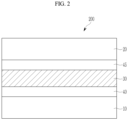
- FIG. 2 a photoelectric device according to some example embodiments is described with reference to FIG. 2 .
- FIG. 2 is a cross-sectional view showing a photoelectric device according to some example embodiments.
- a photoelectric device 200 according to some example embodiments, including the example embodiments shown in FIG. 2 includes a first electrode 10 and a second electrode 20 facing each other, and an active layer 30 between the first electrode 10 and the second electrode 20, like some example embodiments, including the example embodiments shown in FIG. 1 .
- the photoelectric device 200 further includes charge auxiliary layers 40 and 45 between the first electrode 10 and the active layer 30, and the second electrode 20 and the active layer 30, unlike some example embodiments, including the example embodiments shown in FIG. 1 .
- the charge auxiliary layers 40 and 45 may facilitate the transfer of holes and electrons separated from the active layer 30, so as to increase efficiency.
- the charge auxiliary layers 40 and 45 may be at least one of a hole injection layer (HIL) for facilitating hole injection, a hole transport layer (HTL) for facilitating hole transport, an electron blocking layer (EBL) for preventing electron transport, an electron injection layer (EIL) for facilitating electron injection, an electron transport layer (ETL) for facilitating electron transport, or a hole blocking layer (HBL) for preventing hole transport.
- HIL hole injection layer
- HTL hole transport layer
- EBL electron blocking layer
- EIL electron injection layer
- ETL electron transport layer
- HBL hole blocking layer
- the charge auxiliary layers 40 and 45 may include, for example, an organic material, an inorganic material, or an organic/inorganic material.
- the organic material may be an organic compound having hole or electron characteristics
- the inorganic material may be, for example, a metal oxide such as molybdenum oxide, tungsten oxide, nickel oxide, and the like.
- the hole transport layer may include one of, for example, poly(3,4-ethylenedioxythiophene):poly(styrenesulfonate) (PEDOT:PSS), polyarylamine, poly(N-vinylcarbazole), polyaniline, polypyrrole, N,N,N',N'-tetrakis(4-methoxyphenyl)-benzidine (TPD), 4,4'-bis[N-(1-naphthyl)-N-phenyl-amino]biphenyl ( ⁇ -NPD), m-MTDATA, 4,4',4"-tris(N-carbazolyl)-triphenylamine (TCTA), or a combination thereof, but is not limited thereto.
- PEDOT:PSS poly(styrenesulfonate)
- PDOT poly(styrenesulfonate)
- PDOT:PSS poly(styrenesulfonate)
- PDOT:PSS poly
- the electron blocking layer may include one of, for example, poly(3,4-ethylenedioxythiophene):poly(styrenesulfonate) (PEDOT:PSS), polyarylamine, poly(N-vinylcarbazole), polyaniline, polypyrrole, N,N,N',N'-tetrakis(4-methoxyphenyl)-benzidine (TPD), 4,4'-bis[N-(1-naphthyl)-N-phenyl-amino]biphenyl ( ⁇ -NPD), m-MTDATA, 4,4',4"-tris(N-carbazolyl)-triphenylamine (TCTA), or a combination thereof, but is not limited thereto.
- PEDOT:PSS poly(styrenesulfonate)
- PDOT:PSS poly(styrenesulfonate)
- PDOT:PSS poly(styrenesulfonate)
- the electron transport layer may include one of, for example, 1,4,5,8-naphthalene-tetracarboxylic dianhydride (NTCDA), bathocuproine (BCP), LiF, Alq 3 , Gaq 3 , Inq 3 , Znq 2 , Zn(BTZ) 2 , BeBq 2 , or a combination thereof, but is not limited thereto.
- NTCDA 1,4,5,8-naphthalene-tetracarboxylic dianhydride
- BCP bathocuproine
- LiF LiF
- the hole blocking layer may include one of, for example, 1,4,5,8-naphthalene-tetracarboxylic dianhydride (NTCDA), bathocuproine (BCP), LiF, Alq 3 , Gaq 3 , Inq 3 , Znq 2 , Zn(BTZ) 2 , BeBq 2 , or a combination thereof, but is not limited thereto.
- NTCDA 1,4,5,8-naphthalene-tetracarboxylic dianhydride
- BCP bathocuproine
- LiF LiF
- Either one of the charge auxiliary layers 40 or 45 may be omitted.
- the photoelectric device may be applied to various fields, for example a solar cell, an image sensor, a photo-detector, a photo-sensor, and an organic light emitting diode (OLED), but is not limited thereto.
- a solar cell an image sensor, a photo-detector, a photo-sensor, and an organic light emitting diode (OLED), but is not limited thereto.
- OLED organic light emitting diode
- an example of an image sensor including the organic photoelectric device is described referring to drawings.
- an organic CMOS image sensor is described.
- FIG. 3 is a schematic top plan view showing an organic CMOS image sensor according to some example embodiments
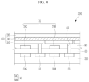
- FIG. 4 is a cross-sectional view showing the organic CMOS image sensor of FIG. 3 .
- an organic CMOS image sensor 300 includes a semiconductor substrate 310 integrated with photo-sensing device 50, which may include photo-sensing devices 50G and 50R, a transmission transistor (not shown), a charge storage 55, a lower insulating layer 60, a color filter layer 70, an upper insulating layer 80, and a photoelectric device 100.
- photo-sensing device 50 may include photo-sensing devices 50G and 50R, a transmission transistor (not shown), a charge storage 55, a lower insulating layer 60, a color filter layer 70, an upper insulating layer 80, and a photoelectric device 100.
- the semiconductor substrate 310 may be a silicon substrate, and is integrated with the photo-sensing device 50, the transmission transistor (not shown), and the charge storage 55.
- the photo-sensing devices 50G and 50R may be photodiodes.
- the photo-sensing devices 50G and 50R, the transmission transistor, and/or the charge storage 55 may be integrated in each pixel, and as shown in the drawing, the photo-sensing devices 50G and 50R may be respectively included in a green pixel and a red pixel and the charge storage 55 may be included in a blue pixel.
- the photo-sensing devices 50G and 50R sense light, the information sensed by the photo-sensing devices may be transferred by the transmission transistor, the charge storage 55 is electrically connected to the photoelectric device 100, and the information of the charge storage 55 may be transferred by the transmission transistor.
- the photo-sensing devices 50G and 50R are, for example, arranged in parallel without limitation, and the green photo-sensing device 50G and the red photo-sensing device 50R may be stacked in a vertical direction.
- a metal wire (not shown) and a pad (not shown) are formed on the semiconductor substrate 310.
- the metal wire and pad may be made of a metal having low resistivity, for example, aluminum (Al), copper (Cu), silver (Ag), and alloys thereof, but are not limited thereto. Further, it is not limited to the structure, and the metal wire and pad may be positioned under the photo-sensing devices 50G and 50R.
- the lower insulating layer 60 is formed on the metal wire and the pad.
- the lower insulating layer 60 may be made of an inorganic insulating material such as a silicon oxide and/or a silicon nitride, or a low dielectric constant (low K) material such as SiC, SiCOH, SiCO, and SiOF.
- the lower insulating layer 60 has a trench exposing the charge storage 55. The trench may be filled with fillers.
- a color filter layer 70 is formed on the lower insulating layer 60.
- the color filter layer 70 includes a green filter 70G formed in the green pixel and selectively transmitting green light and a red filter 70R formed in the red pixel and selectively transmitting red light.
- a cyan filter and a yellow filter may be disposed instead of the green filter 70G and red filter 70R.
- a blue filter is not included, but a blue filter may be further included.
- the color filter layer 70 may be omitted.
- the green photo-sensing device 50G and the red photo-sensing device 50R may selectively absorb light in each wavelength region depending on their stack depth, and the color filter layer 70 may not be equipped.
- the upper insulating layer 80 is formed on the color filter layer 70.
- the upper insulating layer 80 eliminates a step caused by the color filter layer 70 and smoothens the surface.
- the upper insulating layer 80 and the lower insulating layer 60 may include a contact hole (not shown) exposing a pad, and a through-hole 85 exposing the charge storage 55 of the blue pixel.
- the aforementioned photoelectric device 100 is formed on the upper insulating layer 80.
- the photoelectric device 100 includes the first electrode 10, the active layer 30, and the second electrode 20 as described above.
- the first electrode 10 and the second electrode 20 may be transparent electrodes, and the active layer 30 is the same as described above.
- the active layer 30 selectively absorbs and/or senses light in a blue wavelength region and replaces a color filter of a blue pixel.
- the light in a blue wavelength region may be mainly absorbed in the active layer 30 and photoelectrically converted, while the light in the rest of the wavelength regions passes through first electrode 10 and may be sensed in the photo-sensing devices 50G and 50R.
- the photoelectric devices configured to selectively absorb light in a blue wavelength region are stacked and thereby a size of an image sensor may be decreased and a down-sized image sensor may be realized.
- the compound represented by the Chemical Formula 1 is used as a p-type semiconductor compound, aggregation between compounds in a thin film state is inhibited, and thereby light absorption characteristics depending on a wavelength may be maintained. Thereby, blue wavelength selectivity may be maintained, crosstalk caused by unnecessary absorption of other light except a blue wavelength region may be decreased and sensitivity may be increased.
- additional color filters may be further disposed on the photoelectric device 100.
- the additional color filters may include a green filter 70G and a red filter 70R or a cyan filter and a yellow filter.
- FIG. 5 is a schematic cross-sectional view showing an organic CMOS image sensor according to some example embodiments.
- an organic CMOS image sensor 400 has the same structure as FIG. 4 except that a color filter layer 72 including the green filter 72G and the red filter 72R is disposed on the photoelectric device 100. Instead of the green filter 72G and the red filter 72R, a cyan filter and a yellow filter may be disposed respectively.
- FIGS. 4 and 5 the photoelectric device 100 of FIG. 1 is included, but it is not limited thereto, and thus the photoelectric device 200 of FIG. 2 may be applied in the same manner.
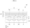
- FIG. 6 is a cross-sectional view showing an organic CMOS image sensor 500 to which the photoelectric device 200 is applied.
- the organic CMOS image sensor 500 includes a semiconductor substrate 310 integrated with photo-sensing devices 50G and 50R, a transmission transistor (not shown), a charge storage 55, an insulating layer 80, and a photoelectric device 200, like some example embodiments, including the example embodiments shown in FIG. 4 .
- the organic CMOS image sensor 500 includes the photoelectric device 200, unlike some example embodiments, including the example embodiments shown in FIG. 4 , which include the photoelectric device 100.
- FIG. 7 is a schematic view showing an organic CMOS image sensor according to some example embodiments.
- the organic CMOS image sensor 600 includes a semiconductor substrate 310 integrated with photo-sensing devices 50G and 50R, a transmission transistor (not shown), a charge storage 55, an insulating layer 80, and a photoelectric device 100, like some example embodiments, including the example embodiments shown in FIG. 5 .
- the organic CMOS image sensor 600 includes the green photo-sensing device 50G and the red photo-sensing device 50R that are stacked and does not include a color filter layer 70, unlike some example embodiments, including the example embodiments shown in FIG. 5 .
- the green photo-sensing device 50G and the red photo-sensing device 50R are electrically connected with the charge storage 55, and the information of the charge storage 55 may be transferred by the transmission transistor (not shown).
- the green photo-sensing device 50G and the red photo-sensing device 50R may selectively absorb light in each wavelength region depending on a stack depth.
- the photoelectric devices configured to selectively absorb light in a blue wavelength region are stacked and the red photo-sensing device and the green photo-sensing device are stacked, and thereby a size of an image sensor may be decreased and a down-sized image sensor may be realized.
- the photoelectric device 100 has improved blue wavelength selectivity, and crosstalk caused by unnecessary absorption light in a wavelength region except blue may be decreased while increasing sensitivity.
- the photoelectric device 100 of FIG. 1 is included, but it is not limited thereto, and thus the photoelectric device 200 of FIG. 2 may be applied in the same manner.
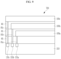
- FIG. 8 is a plan view schematically illustrating an organic CMOS image sensor according to some example embodiments and FIG. 9 is a cross-sectional view of the organic CMOS image sensor of FIG. 8
- the organic CMOS image sensor 700 includes a red photoelectric device (R) configured to selectively absorb light in a red wavelength region, a green photoelectric device (G) configured to selectively absorb light in a green wavelength region, and a blue photoelectric device (B) configured to selectively absorb light in a blue wavelength region that are stacked.
- R red photoelectric device
- G green photoelectric device
- B blue photoelectric device
- the image sensor 700 includes a semiconductor substrate 310, a lower insulating layer 60, an intermediate insulating layer 65, an upper insulating layer 80, a first device 100a, and a second device 100b, and the third device 100c.
- the semiconductor substrate 310 may be a silicon substrate, and a transmission transistor (not shown) and charge storages 155a, 155b, and 155c are integrated therein.
- Metal wires (not shown) and pads (not shown) are formed on the semiconductor substrate 310, and the lower insulating layer 60 is formed on the metal wires and the pads.
- the first device 100a, the second device 100b, and the third device 100c are sequentially formed on the lower insulating layer 60.
- the first, second, and third devices 100a, 100b, and 100c may each independently be the photoelectric devices 100 and 200 of FIG. 1 or 2 . Detailed descriptions of the photoelectric devices 100 and 200 are the same as described above.
- the first electrode 10 and the second electrode 20 of the photoelectric devices 100 and 200 may be connected to the charge storages 155a, 155b, and 155c.
- the active layer 30 of the first device 100a may be a photoelectric conversion device that selectively absorbs light in any one wavelength region of red, blue, or green to photoelectrically convert the light.
- the first device 100a may be a red photoelectric conversion device.
- the first electrode 10 and the second electrode 20 of the first device 100a may be electrically connected to the first charge storage 155a.
- the intermediate insulating layer 65 may be formed on the first device100a and the second device 100b may be formed on the intermediate insulating layer 65.
- the active layer 30 of the second device 100b may be a photoelectric conversion device that selectively absorbs light in any one wavelength region of red, blue, or green to photoelectrically convert the light.
- the second device 100b may be a green photoelectric conversion device.
- the first electrode 10 and the second electrode 20 of the second device 100b may be electrically connected to the second charge storage 155b.
- the upper insulating layer 80 is formed on the second device 100b.
- the lower insulating layer 60, the intermediate insulating layer 65, and the upper insulating layer 80 have a plurality of through-holes 85a, 85b, and 85c exposing the charge storages 155a, 155b, and 155c.
- the third device 100c is formed on the upper insulating layer 80.
- the active layer 30 of the third device 100c may be a photoelectric conversion device that selectively absorbs light in any one wavelength region of red, blue, or green to photoelectrically convert the light.
- the third device 100c may be a blue photoelectric conversion device.
- the first electrode 10 and the second electrode 20 of the third device 100c may be electrically connected to the third charge storage 155c.
- a focusing lens (not shown) may be further formed on the third device 100c.
- the focusing lens may control the direction of incident light and gather the light in one region.
- the focusing lens may have the shape of, for example, a cylinder or a hemisphere, but is not limited thereto.
- the first device 100a, the second device 100b, and the third device 100c that absorb light in different wavelength regions have a stacked structure, further reducing a size of the image sensor, implementing a down-sized image sensor, and simultaneously increasing sensitivity and reducing a crosstalk.
- the image sensor may be applied to various electronic devices, for example, a mobile phone, a digital camera, and the like but is not limited thereto.
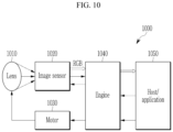
- FIG. 10 is a block diagram of a digital camera including an image sensor according to some example embodiments.
- a digital camera 1000 includes a lens 1010, an image sensor 1020, a motor 1030, and an engine 1040.
- the image sensor 1020 may be any one of the image sensors according to any of the example embodiments, including any of the example embodiments shown in FIGS. 3 to 9 .
- the lens 1010 concentrates incident light on the image sensor 1020.
- the image sensor 1020 generates RGB data for received light through the lens 1010.
- the image sensor 1020 may interface with the engine 1040.
- the motor 1030 may adjust the focus of the lens 1010 or perform shuttering in response to a control signal received from the engine 1040.
- the engine 1040 may control the image sensor 1020 and the motor 1030.
- the engine 1040 may be connected to a host/application 1050.
- FIG. 11 is a schematic diagram showing an electronic device according to some example embodiments.
- an electronic device 1100 may include a processor 1120, a memory 1130, and an image sensor 1140 that are electrically coupled together via a bus 1110.
- the image sensor 1140 may be any one of the image sensors according to any of the example embodiments, including any of the example embodiments shown in FIGS. 3 to 9 .
- the memory 1130 which may be a non-transitory computer readable medium and may store a program of instructions.
- the memory 1130 may be a nonvolatile memory, such as a flash memory, a phase-change random access memory (PRAM), a magneto-resistive RAM (MRAM), a resistive RAM (ReRAM), or a ferro-electric RAM (FRAM), or a volatile memory, such as a static RAM (SRAM), a dynamic RAM (DRAM), or a synchronous DRAM (SDRAM).
- the processor 1120 may execute the stored program of instructions to perform one or more functions.
- the processor 1120 may be configured to process electrical signals generated by the image sensor 1140.
- the processor 1120 may include processing circuitry such as hardware including logic circuits; a hardware/software combination such as a processor executing software; or a combination thereof.
- the processing circuitry more specifically may include, but is not limited to, a central processing unit (CPU), an arithmetic logic unit (ALU), a digital signal processor, a microcomputer, a field programmable gate array (FPGA), a System-on-Chip (SoC), a programmable logic unit, a microprocessor, application-specific integrated circuit (ASIC), etc.
- the processor 1120 may be configured to generate an output (e.g., an image to be displayed on a display interface) based on such processing.
- processor 1120 may be included in, include, and/or implement one or more instances of processing circuitry such as hardware including logic circuits, a hardware/software combination such as a processor executing software; or a combination thereof.
- processing circuitry such as hardware including logic circuits, a hardware/software combination such as a processor executing software; or a combination thereof.
- said one or more instances of processing circuitry may include, but are not limited to, a central processing unit (CPU), an application processor (AP), an arithmetic logic unit (ALU), a graphic processing unit (GPU), a digital signal processor, a microcomputer, a field programmable gate array (FPGA), a System-on-Chip (SoC) a programmable logic unit, a microprocessor, or an application-specific integrated circuit (ASIC), etc.
- CPU central processing unit
- AP application processor
- ALU arithmetic logic unit
- GPU graphic processing unit
- DSP digital signal processor
- microcomputer a field programmable gate array
- FPGA field programmable gate array
- SoC System-on-Chip
- ASIC application-specific integrated circuit
- any of the memories, memory units, or the like as described herein may include a non-transitory computer readable storage device, for example a solid state drive (SSD), storing a program of instructions, and the one or more instances of processing circuitry may be configured to execute the program of instructions to implement the functionality of some or all of any of the processor 1120, memory 1130, motor 1030, engine 1040, or host/application 1050, or the like according to any of the example embodiments as described herein.
- SSD solid state drive
- the HOMO and LUMO energy levels of the compounds according to Synthesis Example 1 and Synthesis Example 2 are measured by cyclic voltammetry.
- the compounds according to Synthesis Example 1 and Synthesis Example 2 are deposited to a thickness of 100 nm on ITO-coated glass at a rate of 0.5 to 1.0 ⁇ /s under high vacuum ( ⁇ 10 -7 Torr) with C60 at a volume ratio of 1:1, respectively, to manufacture each electrode.
- a Princeton Applied Research Potentiostat/Galvanostat Model 273A is placed over a tri-electrode cell assembly containing a working electrode of the above electrode, a counter electrode of platinum wire, and a reference electrode of a silver wire, electricity is applied to the electrodes in a CH 2 Cl 2 /0.1 M Bu 4 NBF 4 solution, and an oxidation-reduction voltage is measured.
- the HOMO energy level is estimated based on the onset oxidation potential (E ox ), and E ox is calibrated using ferrocene (E Fc/Fc+ ). The results are shown in Table 1.
- the compounds according to Synthesis Example 1 and Synthesis Example 2 exhibit excellent selective absorption characteristics of the blue wavelength because the maximum absorption wavelengths are located in the blue region and the full widths at half maximum (FWHMs) thereof are also narrow.
- the compounds may be used as a p-type semiconductor from HOMO, LUMO, and bandgap energies.
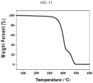
- the thermal stability of the compounds according to Synthesis Example 1 and Synthesis Example 2 is evaluated by measuring the decomposition temperature (T d ) at the time when their weights are reduced by 10 wt% of the total weight using a thermogravimetric analyzer TGA Q5000 (manufactured by TA instruments) (heating rate: 10 °C/min).
- FIGS. 12 and 13 show thermogravimetric analysis results of compounds according to Synthesis Example 1 and Synthesis Example 2, respectively. Referring to FIGS. 12 and 13 , the decomposition temperature of the compound according to Synthesis Example 1 is 334 °C, and the decomposition temperature of the compound according to Synthesis Example 2 is 342 °C.
- An about 150 nm-thick anode is formed by sputtering ITO on a glass substrate, and a 140 nm-thick active layer is formed thereon by codepositing a compound represented by Chemical Formula 1A according to Synthesis Example 1 (p-type semiconductor compound) and C60 (n-type semiconductor compound) in a volume ratio of 1:1.
- a 10 nm-thick molybdenum oxide (MoO x , 0 ⁇ x ⁇ 3) thin film is formed thereon as a charge auxiliary layer.
- a 7 nm-thick cathode is formed by sputtering ITO, manufacturing an organic photoelectric device.
- Photoelectric devices according to Example 2 is manufactured according to the same method as Example 1 except that the compound of Synthesis Example 2 is used instead of the compound according to Synthesis Example 1.
- the photoelectric devices according to Examples 1 and 2 are irradiated with ultraviolet-visible light (UV-Vis) using Cary 5000 UV spectroscopy (manufactured by Varian) to evaluate absorption characteristics (maximum absorption wavelength, full width at half maximum (FWHM)).
- UV-Vis ultraviolet-visible light
- Cary 5000 UV spectroscopy manufactured by Varian
- absorption characteristics maximum absorption wavelength, full width at half maximum (FWHM)
- Table 2 Compound ⁇ max (nm) Full width at half maximum (FWHM) (nm)
- Example 2 Chemical Formula 1B 460 80.5 Comparative Example Color Filter 460 130
- the maximum absorption wavelengths are located in the blue region and full widths at half maximum (FWHM) are narrow, compared with a commercially available color filter (comparative example), which shows their blue wavelength selective absorption characteristics are improved.
- first electrode 20 second electrode 30: active layer 40, 45: charge auxiliary layer 100
- 200 photoelectric device 300, 400, 500, 600, 700: organic CMOS image sensor 310: semiconductor substrate 70G: green filter 70R: red filter 70: color filter layer 85: through-hole 60: lower insulating layer 80: upper insulating layer 50G, 50R: photo-sensing device 55: charge storage
Landscapes
- Chemical & Material Sciences (AREA)
- Physics & Mathematics (AREA)
- Engineering & Computer Science (AREA)
- Organic Chemistry (AREA)
- Materials Engineering (AREA)
- Spectroscopy & Molecular Physics (AREA)
- General Physics & Mathematics (AREA)
- Optics & Photonics (AREA)
- Health & Medical Sciences (AREA)
- Chemical Kinetics & Catalysis (AREA)
- Medicinal Chemistry (AREA)
- Polymers & Plastics (AREA)
- Manufacturing & Machinery (AREA)
- Electromagnetism (AREA)
- Plural Heterocyclic Compounds (AREA)
- Electroluminescent Light Sources (AREA)
Claims (10)
- Photoelektrische Vorrichtung (100, 200, 300, 400, 500, 600), umfassendeine erste Elektrode (10) und eine zweite Elektrode (20), die einander zugewandt sind, undeine aktive Schicht (30) zwischen der ersten Elektrode und der zweiten Elektrode,wobei die aktive Schicht eine einzelne intrinsische Schicht ist und eine Verbindung beinhaltet, die durch die chemische Formel 1 als ein Halbleiter vom p-Typ und ein Halbleiter vom n-Typ in einem Volumenverhältnis von 1:100 bis 100:1 dargestellt ist:
 wobei in der chemischen Formel 1Ar1 und Ar2 jeweils unabhängig eine substituierte oder unsubstituierte aromatische C5- bis C30-Kohlenwasserstoffgruppe oder eine substituierte oder unsubstituierte heteroaromatische C3-bis C30-Kohlenwasserstoffgruppe sind,Z1 und Z2 jeweils unabhängig O, S, Se, Te oder C(CN)2 sind,R1 und R2 jeweils unabhängig eine substituierte oder unsubstituierte C6- bis C40-Alkylgruppe, eine substituierte oder unsubstituierte C3- bis C30-Cycloalkylgruppe, eine substituierte oder unsubstituierte C3- bis C30-Heterocycloalkylgruppe, eine substituierte oder unsubstituierte C6- bis C30-Arylgruppe oder eine substituierte oder unsubstituierte C3- bis C30-Heteroarylgruppe sind, undRa und Rb jeweils unabhängig Wasserstoff, Deuterium, ein Halogen, eine Cyanogruppe oder eine C1- bis C10-Alkylgruppe sind.
- Photoelektrische Vorrichtung nach Anspruch 1, wobei in der chemischen Formel 1 die substituierte oder unsubstituierte aromatische C5- bis C30-Kohlenwasserstoffgruppe eine substituierte oder unsubstituierte Phenylgruppe, eine substituierte oder unsubstituierte Naphthylgruppe, eine substituierte oder unsubstituierte Anthracenylgruppe, eine substituierte oder unsubstituierte Phenanthrenylgruppe, eine substituierte oder unsubstituierte Naphthacenylgruppe, eine substituierte oder unsubstituierte Pyrenylgruppe, eine substituierte oder unsubstituierte Biphenylgruppe, eine substituierte oder unsubstituierte p-Terphenylgruppe, eine substituierte oder unsubstituierte m-Terphenylgruppe, eine substituierte oder unsubstituierte o-Terphenylgruppe, eine substituierte oder unsubstituierte Chrysenylgruppe, eine substituierte oder unsubstituierte Triphenylenylgruppe, eine substituierte oder unsubstituierte Perylenylgruppe, eine substituierte oder unsubstituierte Fluorenylgruppe oder eine substituierte oder unsubstituierte Indenylgruppe ist; und/oder
wobei in der chemischen Formel 1 die substituierte oder unsubstituierte heteroaromatische C3- bis C30-Kohlenwasserstoffgruppe eine substituierte oder unsubstituierte Furanylgruppe, eine substituierte oder unsubstituierte Thienylgruppe, eine substituierte oder unsubstituierte Selenophenylgruppe, eine substituierte oder unsubstituierte Pyrrolylgruppe, eine substituierte oder unsubstituierte Pyrazolylgruppe, eine substituierte oder unsubstituierte Imidazolylgruppe, eine substituierte oder unsubstituierte Triazolylgruppe, eine substituierte oder unsubstituierte Oxazolylgruppe, eine substituierte oder unsubstituierte Isoxazolylgruppe, eine substituierte oder unsubstituierte Thiazolylgruppe, eine substituierte oder unsubstituierte Isothiazolylgruppe, eine substituierte oder unsubstituierte Oxadiazolylgruppe, eine substituierte oder unsubstituierte Thiadiazolylgruppe, eine substituierte oder unsubstituierte Pyridylgruppe, eine substituierte oder unsubstituierte Pyridinylgruppe, eine substituierte oder unsubstituierte Pyridylgruppe, eine substituierte oder unsubstituierte Pyrimidinylgruppe, eine substituierte oder unsubstituierte Pyrazinylgruppe, eine substituierte oder unsubstituierte Triazinylgruppe, eine substituierte oder unsubstituierte Benzofuranylgruppe, eine substituierte oder unsubstituierte Benzothiophenylgruppe, eine substituierte oder unsubstituierte Benzimidazolylgruppe, eine substituierte oder unsubstituierte Indolylgruppe, eine substituierte oder unsubstituierte Chinolinylgruppe, eine substituierte oder unsubstituierte Isochinolinylgruppe, eine substituierte oder unsubstituierte Chinazolinylgruppe, eine substituierte oder unsubstituierte Phthalazinylgruppe, eine substituierte oder unsubstituierte Chinoxalinylgruppe, eine substituierte oder unsubstituierte Naphthyridinylgruppe, eine substituierte oder unsubstituierte Cinnolinylgruppe, eine substituierte oder unsubstituierte Benzoxazinylgruppe, eine substituierte oder unsubstituierte Benzthiazinylgruppe, eine substituierte oder unsubstituierte Acridinylgruppe, eine substituierte oder unsubstituierte Phenazinylgruppe, eine substituierte oder unsubstituierte Phenothiazinylgruppe, eine substituierte oder unsubstituierte Phenoxazinylgruppe, eine substituierte oder unsubstituierte Dibenzofuranylgruppe, eine substituierte oder unsubstituierte Dibenzothiophenylgruppe, eine substituierte oder unsubstituierte Benzotriazinylgruppe, eine substituierte oder unsubstituierte Pyridopyrazinylgruppe, ein substituiertes oder unsubstituiertes Pyridopyrimidinyl, eine substituierte oder unsubstituierte Pyridopyridazinylgruppe, eine substituierte oder unsubstituierte Benzothienylgruppe oder eine substituierte oder unsubstituierte Benzoselenophenylgruppe ist. - Photoelektrische Vorrichtung nach Anspruch 1 oder 2, wobei in der chemischen Formel 1 die substituierte oder unsubstituierte aromatische C5- bis C30-Kohlenwasserstoffgruppe eine der funktionellen Gruppen der chemischen Formel 1-1 ist:
 wobei in der chemischen Formel 1-1Wasserstoff von -CH- von jedem aromatischen Ring optional durch einen Substituenten einer substituierten oder unsubstituierten C1- bis C20-Alkylgruppe, einer substituierten oder unsubstituierten C1- bis C20-Alkoxygruppe, einer substituierten oder unsubstituierten C6- bis C10-Arylgruppe, einer substituierten oder unsubstituierten C4- bis C10-Heteroarylgruppe, eines Halogens, einer Cyanogruppe, einer cyanohaltigen Gruppe oder einer Kombination davon ersetzt ist, und* eine Verknüpfungsposition angibt; und/oderwobei in der chemischen Formel 1 die substituierte oder unsubstituierte heteroaromatische C3- bis C30-Kohlenwasserstoffgruppe eine der funktionellen Gruppen dargestellt durch die chemische Formel 1-2 ist:

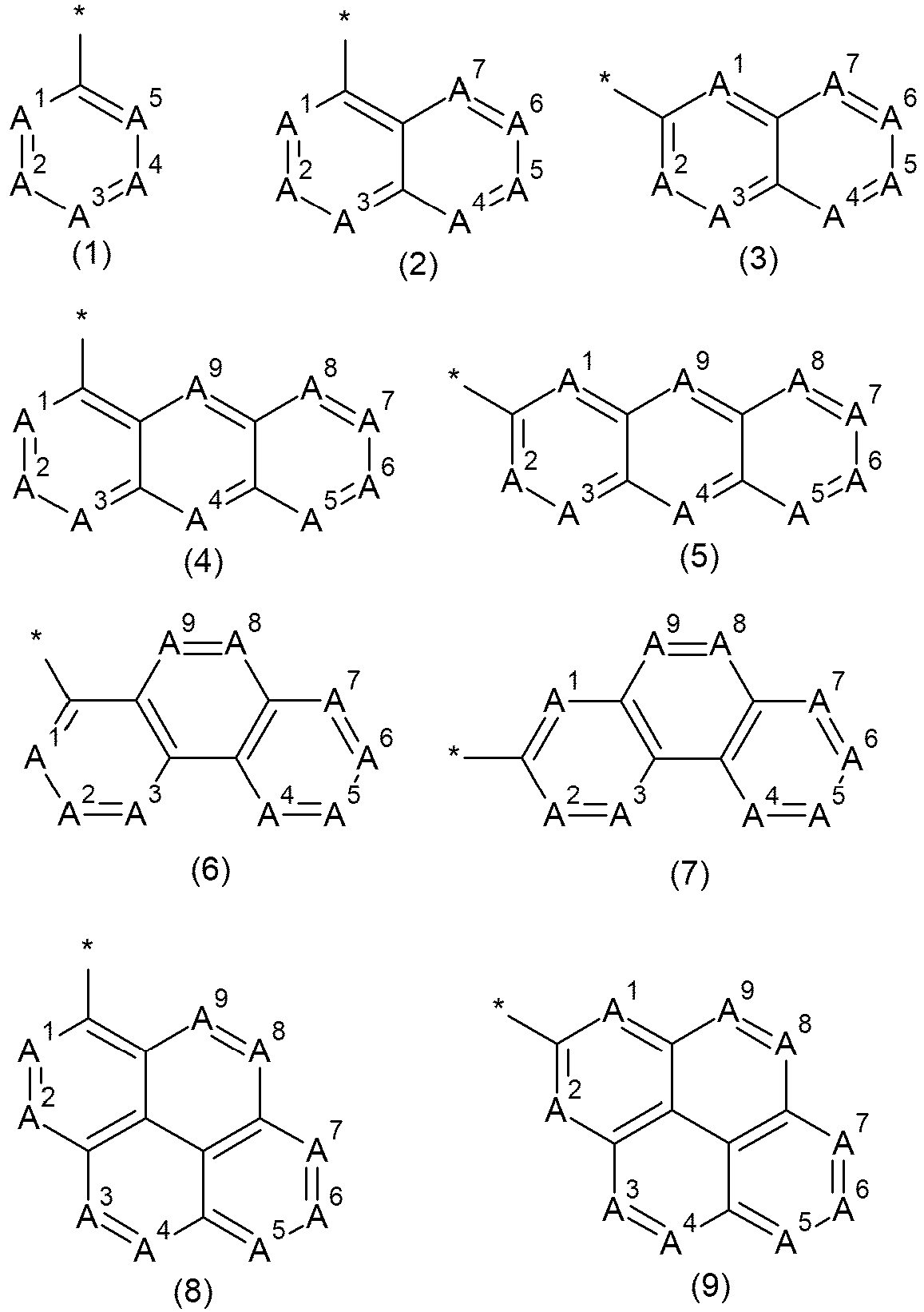 wobei in der chemischen Formel 1-2A1 bis A9 jeweils unabhängig N oder CRk sind, wobei Rk Wasserstoff, Deuterium, eine substituierte oder unsubstituierte C1- bis C20-Alkylgruppe, eine substituierte oder unsubstituierte C1- bis C20-Alkoxygruppe, eine substituierte oder unsubstituierte C6- bis C10-Arylgruppe, eine substituierte oder unsubstituierte C4- bis C10-Heteroarylgruppe, ein Halogen, eine Cyanogruppe, eine cyanohaltige Gruppe oder eine Kombination davon ist,1 bis 3 von A1 bis A5 der chemischen Formel (1) der chemischen Formel 1-2 N sind,1 bis 3 von A1 bis A7 der chemischen Formeln (2) und (3) der chemischen Formel 1-2 N sind,1 bis 4 von A1 bis A9 der chemischen Formeln (4) bis (9) der chemischen Formel 1-2 N sind, und* eine Verknüpfungsposition angibt.
- Photoelektrische Vorrichtung nach einem der Ansprüche 1-3, wobei in der chemischen Formel 1 die substituierte oder unsubstituierte aromatische C5- bis C30-Kohlenwasserstoffgruppe eine der funktionellen Gruppen dargestellt durch die chemische Formel 1-3 ist:
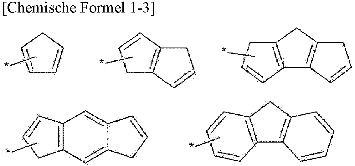 wobei in der chemischen Formel 1-3ein Wasserstoff von -CH- von jedem aromatischen Ring optional durch einen Substituenten einer substituierten oder unsubstituierten C1- bis C20-Alkylgruppe, einer substituierten oder unsubstituierten C1- bis C20-Alkoxygruppe, einer substituierten oder unsubstituierten C6- bis C10-Arylgruppe, einer substituierten oder unsubstituierten C4- bis C10-Heteroarylgruppe, eines Halogens, einer Cyanogruppe, einer cyanohaltigen Gruppe oder einer Kombination davon ersetzt ist, und* eine Verknüpfungsposition angibt; und/oderwobei in der chemischen Formel 1 die substituierte oder unsubstituierte heteroaromatische C3- bis C30-Kohlenwasserstoffgruppe eine der funktionellen Gruppen dargestellt durch die chemische Formel 1-4 ist:

 wobei in der chemischen Formel 1-4Y1 bis Y3 jeweils unabhängig O, S, Se, Te oder NRa sind, wobei Ra Wasserstoff, Deuterium oder eine substituierte oder unsubstituierte C1- bis C10-Alkylgruppe ist,A1 bis A8 jeweils unabhängig N oder CRk sind, wobei Rk Wasserstoff, Deuterium, eine substituierte oder unsubstituierte C1- bis C20-Alkylgruppe, eine substituierte oder unsubstituierte C1- bis C20-Alkoxygruppe, eine substituierte oder unsubstituierte C6- bis C10-Arylgruppe, eine substituierte oder unsubstituierte C4- bis C10-Heteroarylgruppe, ein Halogen, eine Cyanogruppe, eine cyanohaltige Gruppe oder eine Kombination davon sind,ein Wasserstoff von -CH- von jedem aromatischen Ring optional durch einen Substituenten einer substituierten oder unsubstituierten C1- bis C20-Alkylgruppe, einer substituierten oder unsubstituierten C1- bis C20-Alkoxygruppe, einer substituierten oder unsubstituierten C6- bis C10-Arylgruppe, einer substituierten oder unsubstituierten C4- bis C10-Heteroarylgruppe, eines Halogens, einer Cyanogruppe, einer cyanohaltigen Gruppe oder einer Kombination davon ersetzt ist,in der chemischen Formel (8) der chemischen Formel 1-4 eines von A1 bis A4 ein Verknüpfungsabschnitt ist und zumindest eines von A1 bis A8 Stickstoff (N) ist, und* eine Verknüpfungsposition angibt.
- Photoelektrische Vorrichtung nach einem der Ansprüche 1-4, wobei die aktive Schicht konfiguriert ist, um eine Absorptionskurve mit einer vollen Breite bei halbem Maximum (FWHM) von 50 nm bis 90 nm zu zeigen; und/oderwobei die aktive Schicht konfiguriert ist, um eine Absorptionskurve mit einer zentralen Wellenlänge von weniger als oder gleich 460 nm zu zeigen;wobei die volle Breite bei halbem Maximum (FWHM) und die zentrale Wellenlänge der Absorptionskurve durch UV-Vis-Spektroskopie unter Verwendung eines Dünnfilms gemessen werden.
- Bildsensor, der die photoelektrische Vorrichtung nach einem der Ansprüche 1-5 umfasst.
- Bildsensor nach Anspruch 6, wobei
der Bildsensor Folgendes beinhaltet:ein Halbleitersubstrat, das in einer Vielzahl von ersten Photoerfassungsvorrichtungen, die konfiguriert ist, um Licht in einem grünen Wellenlängenbereich zu erfassen, und einer Vielzahl von zweiten Photoerfassungsvorrichtungen, die konfiguriert ist, um Licht in einem roten Wellenlängenbereich zu erfassen, integriert ist, unddie photoelektrische Vorrichtung auf dem Halbleitersubstrat ist und konfiguriert ist, um selektiv Licht in einem blauen Wellenlängenbereich zu erfassen. - Bildsensor nach Anspruch 7, wobei der Bildsensor ferner eine Farbfilterschicht beinhaltet, die einen Grünfilter, der konfiguriert ist, um selektiv Licht in dem grünen Wellenlängenbereich zu übertragen, und einen Rotfilter, der konfiguriert ist, um selektiv Licht in dem roten Wellenlängenbereich zu übertragen, beinhaltet; und/oder
wobei die Vielzahl von ersten Photoerfassungsvorrichtungen und die Vielzahl von zweiten Photoerfassungsvorrichtungen in einer vertikalen Richtung in dem Halbleitersubstrat gestapelt sind. - Bildsensor nach einem der Ansprüche 6-8, wobeidie photoelektrische Vorrichtung eine blaue photoelektrische Vorrichtung ist, die konfiguriert ist, um selektiv Licht in einem blauen Wellenlängenbereich zu erfassen,der Bildsensor eine rote photoelektrische Vorrichtung, die konfiguriert ist, um selektiv Licht in einem roten Wellenlängenbereich zu erfassen, eine grüne photoelektrische Vorrichtung, die konfiguriert ist, um selektiv Licht in einem grünen Wellenlängenbereich zu erfassen, und die blaue photoelektrische Vorrichtung beinhaltet, undwobei die grüne photoelektrische Vorrichtung, die blaue photoelektrische Vorrichtung und die rote photoelektrische Vorrichtung gestapelt sind.
- Elektronische Vorrichtung, die den Bildsensor nach einem der Ansprüche 6-9 umfasst.
Applications Claiming Priority (1)
| Application Number | Priority Date | Filing Date | Title |
|---|---|---|---|
| KR1020200188467A KR20220096214A (ko) | 2020-12-30 | 2020-12-30 | 청색 흡수용 필름, 광전 소자 및 이를 포함하는 이미지 센서와 전자 장치 |
Publications (2)
| Publication Number | Publication Date |
|---|---|
| EP4024488A1 EP4024488A1 (de) | 2022-07-06 |
| EP4024488B1 true EP4024488B1 (de) | 2025-05-21 |
Family
ID=80225572
Family Applications (1)
| Application Number | Title | Priority Date | Filing Date |
|---|---|---|---|
| EP21218364.4A Active EP4024488B1 (de) | 2020-12-30 | 2021-12-30 | Photoelektrische vorrichtung, bildsensor und elektronische vorrichtung damit |
Country Status (3)
| Country | Link |
|---|---|
| US (1) | US12439815B2 (de) |
| EP (1) | EP4024488B1 (de) |
| KR (1) | KR20220096214A (de) |
Families Citing this family (1)
| Publication number | Priority date | Publication date | Assignee | Title |
|---|---|---|---|---|
| KR102883133B1 (ko) * | 2022-11-25 | 2025-11-10 | 서울대학교산학협력단 | 근적외선 흡수 필터용 화합물, 이를 포함하는 조성물 및 이의 경화물을 포함하는 근적외선 흡수 필름 |
Citations (1)
| Publication number | Priority date | Publication date | Assignee | Title |
|---|---|---|---|---|
| US20200152888A1 (en) * | 2018-11-13 | 2020-05-14 | Samsung Electronics Co., Ltd. | Organic device and image sensor |
Family Cites Families (4)
| Publication number | Priority date | Publication date | Assignee | Title |
|---|---|---|---|---|
| JP5520560B2 (ja) | 2009-09-29 | 2014-06-11 | 富士フイルム株式会社 | 光電変換素子、光電変換素子材料、光センサ、及び撮像素子 |
| JP6047108B2 (ja) | 2014-01-31 | 2016-12-21 | 富士フイルム株式会社 | 光電変換素子、撮像素子、光センサ |
| US11603431B2 (en) | 2016-02-04 | 2023-03-14 | Raynergy Tek Incorporation | Organic semiconductors |
| KR102106295B1 (ko) | 2018-04-19 | 2020-05-04 | 서울대학교산학협력단 | 형광체 단분자 화합물, 이를 이용한 유기 트랜지스터 및 이를 이용한 물 분해 수소 생산 광 촉매 시스템 |
-
2020
- 2020-12-30 KR KR1020200188467A patent/KR20220096214A/ko active Pending
-
2021
- 2021-12-30 US US17/565,726 patent/US12439815B2/en active Active
- 2021-12-30 EP EP21218364.4A patent/EP4024488B1/de active Active
Patent Citations (1)
| Publication number | Priority date | Publication date | Assignee | Title |
|---|---|---|---|---|
| US20200152888A1 (en) * | 2018-11-13 | 2020-05-14 | Samsung Electronics Co., Ltd. | Organic device and image sensor |
Also Published As
| Publication number | Publication date |
|---|---|
| EP4024488A1 (de) | 2022-07-06 |
| US12439815B2 (en) | 2025-10-07 |
| KR20220096214A (ko) | 2022-07-07 |
| US20220209134A1 (en) | 2022-06-30 |
Similar Documents
| Publication | Publication Date | Title |
|---|---|---|
| EP3961737B1 (de) | Zusammensetzung für fotoelektrische vorrichtung sowie bildsensor und elektronisches gerät damit | |
| EP3848374B1 (de) | Verbindung und fotoelektrische vorrichtung, bildsensor und elektronische vorrichtung damit | |
| EP3018723B1 (de) | Verbindung für organische fotoelektrische vorrichtung und bildsensor mit einer organischen fotoelektrischen vorrichtung | |
| EP3026722B1 (de) | Verbindung für organische fotoelektrische vorrichtung und bildsensor einer organischen fotoelektrischen vorrichtung sowie elektronische vorrichtung damit | |
| EP3173410B1 (de) | Verbindung für organische fotoelektrische vorrichtung und organische fotoelektrische vorrichtung, bildsensor und elektronische vorrichtung damit | |
| EP3228623B1 (de) | Verbindung, organische photoelektrische vorrichtung, bildsensor und elektronische vorrichtung | |
| JP6721980B2 (ja) | 有機光電素子、並びにイメージセンサー及びこれを備える電子装置 | |
| US12365697B2 (en) | Compound and photoelectric device, image sensor, and electronic device including the same | |
| JP6047108B2 (ja) | 光電変換素子、撮像素子、光センサ | |
| TW201631815A (zh) | 光電轉換元件及使用其的影像感測器 | |
| EP4024484B1 (de) | Zusammensetzung für fotoelektrische vorrichtung sowie fotoelektrische vorrichtung, bildsensor und elektronische vorrichtung damit | |
| KR102798537B1 (ko) | 화합물, 및 이를 포함하는 광전 소자, 이미지 센서 및 전자 장치 | |
| US12439815B2 (en) | Blue light absorbing film, and photoelectric device, image sensor and electronic device including the same | |
| EP4458829A1 (de) | 4h,8h-thieno[3',2':5,6]pyrido[3,2,1-de]acridin-derivate mit hohen extinktionskoeffizienten zur verwendung als materialien in fotoelektronischen geräten und bildsensoren | |
| US12084439B2 (en) | Compound and photoelectric device, image sensor, and electronic device including the same | |
| KR102558974B1 (ko) | 유기 광전 소자, 이미지 센서 및 전자장치 | |
| EP3805241A1 (de) | Verbindung und fotoelektrische vorrichtung, bildsensor und elektronische vorrichtung damit |
Legal Events
| Date | Code | Title | Description |
|---|---|---|---|
| PUAI | Public reference made under article 153(3) epc to a published international application that has entered the european phase |
Free format text: ORIGINAL CODE: 0009012 |
|
| STAA | Information on the status of an ep patent application or granted ep patent |
Free format text: STATUS: THE APPLICATION HAS BEEN PUBLISHED |
|
| AK | Designated contracting states |
Kind code of ref document: A1 Designated state(s): AL AT BE BG CH CY CZ DE DK EE ES FI FR GB GR HR HU IE IS IT LI LT LU LV MC MK MT NL NO PL PT RO RS SE SI SK SM TR |
|
| STAA | Information on the status of an ep patent application or granted ep patent |
Free format text: STATUS: REQUEST FOR EXAMINATION WAS MADE |
|
| 17P | Request for examination filed |
Effective date: 20230106 |
|
| RBV | Designated contracting states (corrected) |
Designated state(s): AL AT BE BG CH CY CZ DE DK EE ES FI FR GB GR HR HU IE IS IT LI LT LU LV MC MK MT NL NO PL PT RO RS SE SI SK SM TR |
|
| P01 | Opt-out of the competence of the unified patent court (upc) registered |
Effective date: 20230530 |
|
| STAA | Information on the status of an ep patent application or granted ep patent |
Free format text: STATUS: EXAMINATION IS IN PROGRESS |
|
| 17Q | First examination report despatched |
Effective date: 20240422 |
|
| REG | Reference to a national code |
Ref country code: DE Ipc: H10K0085600000 Ref country code: DE Ref legal event code: R079 Ref document number: 602021031068 Country of ref document: DE Free format text: PREVIOUS MAIN CLASS: H01L0051460000 Ipc: H10K0085600000 |
|
| GRAP | Despatch of communication of intention to grant a patent |
Free format text: ORIGINAL CODE: EPIDOSNIGR1 |
|
| STAA | Information on the status of an ep patent application or granted ep patent |
Free format text: STATUS: GRANT OF PATENT IS INTENDED |
|
| RIC1 | Information provided on ipc code assigned before grant |
Ipc: H10K 39/32 20230101ALN20241115BHEP Ipc: H10K 30/30 20230101ALN20241115BHEP Ipc: H10K 85/60 20230101AFI20241115BHEP |
|
| INTG | Intention to grant announced |
Effective date: 20241211 |
|
| RAP3 | Party data changed (applicant data changed or rights of an application transferred) |
Owner name: SEOUL NATIONAL UNIVERSITY R & DB FOUNDATION Owner name: SAMSUNG ELECTRONICS CO., LTD. |
|
| GRAS | Grant fee paid |
Free format text: ORIGINAL CODE: EPIDOSNIGR3 |
|
| GRAA | (expected) grant |
Free format text: ORIGINAL CODE: 0009210 |
|
| STAA | Information on the status of an ep patent application or granted ep patent |
Free format text: STATUS: THE PATENT HAS BEEN GRANTED |
|
| AK | Designated contracting states |
Kind code of ref document: B1 Designated state(s): AL AT BE BG CH CY CZ DE DK EE ES FI FR GB GR HR HU IE IS IT LI LT LU LV MC MK MT NL NO PL PT RO RS SE SI SK SM TR |
|
| REG | Reference to a national code |
Ref country code: GB Ref legal event code: FG4D |
|
| REG | Reference to a national code |
Ref country code: CH Ref legal event code: EP |
|
| REG | Reference to a national code |
Ref country code: DE Ref legal event code: R096 Ref document number: 602021031068 Country of ref document: DE |
|
| REG | Reference to a national code |
Ref country code: IE Ref legal event code: FG4D |
|
| REG | Reference to a national code |
Ref country code: NL Ref legal event code: MP Effective date: 20250521 |
|
| PG25 | Lapsed in a contracting state [announced via postgrant information from national office to epo] |
Ref country code: FI Free format text: LAPSE BECAUSE OF FAILURE TO SUBMIT A TRANSLATION OF THE DESCRIPTION OR TO PAY THE FEE WITHIN THE PRESCRIBED TIME-LIMIT Effective date: 20250521 Ref country code: PT Free format text: LAPSE BECAUSE OF FAILURE TO SUBMIT A TRANSLATION OF THE DESCRIPTION OR TO PAY THE FEE WITHIN THE PRESCRIBED TIME-LIMIT Effective date: 20250922 Ref country code: ES Free format text: LAPSE BECAUSE OF FAILURE TO SUBMIT A TRANSLATION OF THE DESCRIPTION OR TO PAY THE FEE WITHIN THE PRESCRIBED TIME-LIMIT Effective date: 20250521 |
|
| REG | Reference to a national code |
Ref country code: LT Ref legal event code: MG9D |
|
| PG25 | Lapsed in a contracting state [announced via postgrant information from national office to epo] |
Ref country code: NO Free format text: LAPSE BECAUSE OF FAILURE TO SUBMIT A TRANSLATION OF THE DESCRIPTION OR TO PAY THE FEE WITHIN THE PRESCRIBED TIME-LIMIT Effective date: 20250821 Ref country code: GR Free format text: LAPSE BECAUSE OF FAILURE TO SUBMIT A TRANSLATION OF THE DESCRIPTION OR TO PAY THE FEE WITHIN THE PRESCRIBED TIME-LIMIT Effective date: 20250822 |
|
| PG25 | Lapsed in a contracting state [announced via postgrant information from national office to epo] |
Ref country code: PL Free format text: LAPSE BECAUSE OF FAILURE TO SUBMIT A TRANSLATION OF THE DESCRIPTION OR TO PAY THE FEE WITHIN THE PRESCRIBED TIME-LIMIT Effective date: 20250521 Ref country code: NL Free format text: LAPSE BECAUSE OF FAILURE TO SUBMIT A TRANSLATION OF THE DESCRIPTION OR TO PAY THE FEE WITHIN THE PRESCRIBED TIME-LIMIT Effective date: 20250521 |
|
| PG25 | Lapsed in a contracting state [announced via postgrant information from national office to epo] |
Ref country code: BG Free format text: LAPSE BECAUSE OF FAILURE TO SUBMIT A TRANSLATION OF THE DESCRIPTION OR TO PAY THE FEE WITHIN THE PRESCRIBED TIME-LIMIT Effective date: 20250521 |
|
| PG25 | Lapsed in a contracting state [announced via postgrant information from national office to epo] |
Ref country code: HR Free format text: LAPSE BECAUSE OF FAILURE TO SUBMIT A TRANSLATION OF THE DESCRIPTION OR TO PAY THE FEE WITHIN THE PRESCRIBED TIME-LIMIT Effective date: 20250521 |
|
| PG25 | Lapsed in a contracting state [announced via postgrant information from national office to epo] |
Ref country code: RS Free format text: LAPSE BECAUSE OF FAILURE TO SUBMIT A TRANSLATION OF THE DESCRIPTION OR TO PAY THE FEE WITHIN THE PRESCRIBED TIME-LIMIT Effective date: 20250821 |
|
| PG25 | Lapsed in a contracting state [announced via postgrant information from national office to epo] |
Ref country code: IS Free format text: LAPSE BECAUSE OF FAILURE TO SUBMIT A TRANSLATION OF THE DESCRIPTION OR TO PAY THE FEE WITHIN THE PRESCRIBED TIME-LIMIT Effective date: 20250921 |
|
| PG25 | Lapsed in a contracting state [announced via postgrant information from national office to epo] |
Ref country code: LV Free format text: LAPSE BECAUSE OF FAILURE TO SUBMIT A TRANSLATION OF THE DESCRIPTION OR TO PAY THE FEE WITHIN THE PRESCRIBED TIME-LIMIT Effective date: 20250521 |
|
| REG | Reference to a national code |
Ref country code: AT Ref legal event code: MK05 Ref document number: 1798062 Country of ref document: AT Kind code of ref document: T Effective date: 20250521 |
|
| PGFP | Annual fee paid to national office [announced via postgrant information from national office to epo] |
Ref country code: DE Payment date: 20251111 Year of fee payment: 5 |
|
| PGFP | Annual fee paid to national office [announced via postgrant information from national office to epo] |
Ref country code: GB Payment date: 20251113 Year of fee payment: 5 |
|
| PG25 | Lapsed in a contracting state [announced via postgrant information from national office to epo] |
Ref country code: DK Free format text: LAPSE BECAUSE OF FAILURE TO SUBMIT A TRANSLATION OF THE DESCRIPTION OR TO PAY THE FEE WITHIN THE PRESCRIBED TIME-LIMIT Effective date: 20250521 Ref country code: AT Free format text: LAPSE BECAUSE OF FAILURE TO SUBMIT A TRANSLATION OF THE DESCRIPTION OR TO PAY THE FEE WITHIN THE PRESCRIBED TIME-LIMIT Effective date: 20250521 Ref country code: SM Free format text: LAPSE BECAUSE OF FAILURE TO SUBMIT A TRANSLATION OF THE DESCRIPTION OR TO PAY THE FEE WITHIN THE PRESCRIBED TIME-LIMIT Effective date: 20250521 |
|
| PGFP | Annual fee paid to national office [announced via postgrant information from national office to epo] |
Ref country code: FR Payment date: 20251124 Year of fee payment: 5 |
|
| PG25 | Lapsed in a contracting state [announced via postgrant information from national office to epo] |
Ref country code: CZ Free format text: LAPSE BECAUSE OF FAILURE TO SUBMIT A TRANSLATION OF THE DESCRIPTION OR TO PAY THE FEE WITHIN THE PRESCRIBED TIME-LIMIT Effective date: 20250521 |
|
| PG25 | Lapsed in a contracting state [announced via postgrant information from national office to epo] |
Ref country code: EE Free format text: LAPSE BECAUSE OF FAILURE TO SUBMIT A TRANSLATION OF THE DESCRIPTION OR TO PAY THE FEE WITHIN THE PRESCRIBED TIME-LIMIT Effective date: 20250521 |
|
| PG25 | Lapsed in a contracting state [announced via postgrant information from national office to epo] |
Ref country code: SK Free format text: LAPSE BECAUSE OF FAILURE TO SUBMIT A TRANSLATION OF THE DESCRIPTION OR TO PAY THE FEE WITHIN THE PRESCRIBED TIME-LIMIT Effective date: 20250521 Ref country code: RO Free format text: LAPSE BECAUSE OF FAILURE TO SUBMIT A TRANSLATION OF THE DESCRIPTION OR TO PAY THE FEE WITHIN THE PRESCRIBED TIME-LIMIT Effective date: 20250521 |
|
| PG25 | Lapsed in a contracting state [announced via postgrant information from national office to epo] |
Ref country code: IT Free format text: LAPSE BECAUSE OF FAILURE TO SUBMIT A TRANSLATION OF THE DESCRIPTION OR TO PAY THE FEE WITHIN THE PRESCRIBED TIME-LIMIT Effective date: 20250521 |
|
| REG | Reference to a national code |
Ref country code: DE Ref legal event code: R097 Ref document number: 602021031068 Country of ref document: DE |
|
| PLBE | No opposition filed within time limit |
Free format text: ORIGINAL CODE: 0009261 |
|
| STAA | Information on the status of an ep patent application or granted ep patent |
Free format text: STATUS: NO OPPOSITION FILED WITHIN TIME LIMIT |
|
| REG | Reference to a national code |
Ref country code: CH Ref legal event code: L10 Free format text: ST27 STATUS EVENT CODE: U-0-0-L10-L00 (AS PROVIDED BY THE NATIONAL OFFICE) Effective date: 20260402 |
|
| 26N | No opposition filed |
Effective date: 20260224 |
|
| PG25 | Lapsed in a contracting state [announced via postgrant information from national office to epo] |
Ref country code: LT Free format text: LAPSE BECAUSE OF FAILURE TO SUBMIT A TRANSLATION OF THE DESCRIPTION OR TO PAY THE FEE WITHIN THE PRESCRIBED TIME-LIMIT Effective date: 20250521 |
|
| PG25 | Lapsed in a contracting state [announced via postgrant information from national office to epo] |
Ref country code: MC Free format text: LAPSE BECAUSE OF FAILURE TO SUBMIT A TRANSLATION OF THE DESCRIPTION OR TO PAY THE FEE WITHIN THE PRESCRIBED TIME-LIMIT Effective date: 20250521 |
|
| REG | Reference to a national code |
Ref country code: CH Ref legal event code: H13 Free format text: ST27 STATUS EVENT CODE: U-0-0-H10-H13 (AS PROVIDED BY THE NATIONAL OFFICE) Effective date: 20260723 |
|
| PG25 | Lapsed in a contracting state [announced via postgrant information from national office to epo] |
Ref country code: SE Free format text: LAPSE BECAUSE OF FAILURE TO SUBMIT A TRANSLATION OF THE DESCRIPTION OR TO PAY THE FEE WITHIN THE PRESCRIBED TIME-LIMIT Effective date: 20250521 |