EP4024064A1 - Gate detection circuit of insulated gate bipolar transistor - Google Patents
Gate detection circuit of insulated gate bipolar transistor Download PDFInfo
- Publication number
- EP4024064A1 EP4024064A1 EP20894755.6A EP20894755A EP4024064A1 EP 4024064 A1 EP4024064 A1 EP 4024064A1 EP 20894755 A EP20894755 A EP 20894755A EP 4024064 A1 EP4024064 A1 EP 4024064A1
- Authority
- EP
- European Patent Office
- Prior art keywords
- bipolar transistor
- voltage
- insulated gate
- gate
- gate bipolar
- Prior art date
- Legal status (The legal status is an assumption and is not a legal conclusion. Google has not performed a legal analysis and makes no representation as to the accuracy of the status listed.)
- Granted
Links
Images

Classifications
-
- G—PHYSICS
- G01—MEASURING; TESTING
- G01R—MEASURING ELECTRIC VARIABLES; MEASURING MAGNETIC VARIABLES
- G01R31/00—Arrangements for testing electric properties; Arrangements for locating electric faults; Arrangements for electrical testing characterised by what is being tested not provided for elsewhere
- G01R31/26—Testing of individual semiconductor devices
- G01R31/2607—Circuits therefor
- G01R31/2608—Circuits therefor for testing bipolar transistors
-
- G—PHYSICS
- G01—MEASURING; TESTING
- G01R—MEASURING ELECTRIC VARIABLES; MEASURING MAGNETIC VARIABLES
- G01R19/00—Arrangements for measuring currents or voltages or for indicating presence or sign thereof
- G01R19/0038—Circuits for comparing several input signals and for indicating the result of this comparison, e.g. equal, different, greater, smaller (comparing pulses or pulse trains according to amplitude)
-
- G—PHYSICS
- G01—MEASURING; TESTING
- G01R—MEASURING ELECTRIC VARIABLES; MEASURING MAGNETIC VARIABLES
- G01R19/00—Arrangements for measuring currents or voltages or for indicating presence or sign thereof
- G01R19/165—Indicating that current or voltage is either above or below a predetermined value or within or outside a predetermined range of values
- G01R19/16566—Circuits and arrangements for comparing voltage or current with one or several thresholds and for indicating the result not covered by subgroups G01R19/16504, G01R19/16528, G01R19/16533
- G01R19/1659—Circuits and arrangements for comparing voltage or current with one or several thresholds and for indicating the result not covered by subgroups G01R19/16504, G01R19/16528, G01R19/16533 to indicate that the value is within or outside a predetermined range of values (window)
-
- G—PHYSICS
- G01—MEASURING; TESTING
- G01R—MEASURING ELECTRIC VARIABLES; MEASURING MAGNETIC VARIABLES
- G01R29/00—Arrangements for measuring or indicating electric quantities not covered by groups G01R19/00 - G01R27/00
- G01R29/02—Measuring characteristics of individual pulses, e.g. deviation from pulse flatness, rise time or duration
- G01R29/027—Indicating that a pulse characteristic is either above or below a predetermined value or within or beyond a predetermined range of values
-
- G—PHYSICS
- G01—MEASURING; TESTING
- G01R—MEASURING ELECTRIC VARIABLES; MEASURING MAGNETIC VARIABLES
- G01R31/00—Arrangements for testing electric properties; Arrangements for locating electric faults; Arrangements for electrical testing characterised by what is being tested not provided for elsewhere
- G01R31/26—Testing of individual semiconductor devices
- G01R31/2607—Circuits therefor
- G01R31/2608—Circuits therefor for testing bipolar transistors
- G01R31/261—Circuits therefor for testing bipolar transistors for measuring break-down voltage or punch through voltage therefor
Definitions
- the present application relates to the technical field of electronic circuits, and more particularly to a gate detection circuit of an insulated gate bipolar transistor.
- the insulated gate bipolar transistor is a composite fully-controlled voltage-driven power semiconductor device composed of a bipolar triode and an insulated gate field effect transistor.
- the units of the IGBT configured for driving are provided with multiple IGBTs, and when one of the gates breaks down, other IGBTs may also be damaged.
- IGBT gate faults there is currently no technology to detect IGBT gate faults.
- the present application aims to provide a gate detection circuit of an insulated gate bipolar transistor to detect the gate fault of the insulated gate bipolar transistor.
- a gate detection circuit of an insulated gate bipolar transistor includes: a pulse shaping circuit, a comparison circuit, and a fault output circuit;
- the pulse shaping circuit is configured for shaping an input signal of a signal input device, and outputting a first square wave signal of a high level and a second square wave signal of a low level when the input signal is at the high level; and outputting a first square wave signal of the low level and a second square wave signal of the high level when the input signal is at the low level;
- the comparison circuit is configured for: comparing a first preset voltage with a voltage of a gate of the insulated gate bipolar transistor when the first square wave signal is at the high level, and outputting a low level when the first preset voltage is greater than the voltage of the gate of the insulated gate bipolar transistor; and comparing a second preset voltage with a voltage of a gate of the insulated gate bipolar transistor when the second square wave signal is at the high level, and outputting a low level when the second preset voltage is lower than the voltage of
- the comparison circuit includes: a first triode, configured to be turned on when the first square wave signal is at the high level; a second triode, configured to be turned on when the second square wave signal is at the high level; a first comparator, connected to the first triode and configured for comparing the first preset voltage with the voltage of the gate of the insulated gate bipolar transistor when the first triode is turned on; and a second comparator, connected to the second triode and configured for comparing the second preset voltage with the voltage of the gate of the insulated gate bipolar transistor when the second triode is turned on.
- the gate detection circuit further includes: an optocoupler isolation circuit, connected between the signal input device and the pulse shaping circuit, and configured for optoelectronic isolation of the input signal.
- the gate detection circuit further includes: a pulse amplification circuit, connected between the pulse shaping circuit and the insulated gate bipolar transistor, and configured for amplifying the first square wave signal to drive the insulated gate bipolar transistor.
- the gate detection circuit further includes: a voltage division circuit, connected to the comparison circuit, and configured for converting a voltage of a power supply into the first preset voltage and the second preset voltage.
- the gate detection circuit further includes: a detection power supply circuit, including:
- the power supply outputs a positive power supply of +15V and a negative power supply of -5V
- the first preset voltage is 7.5V
- the second preset voltage is -2.5V
- the comparison circuit is further configured for: outputting the high level when the first preset voltage is lower than the voltage of the gate of the insulated gate bipolar transistor in a case that the first square wave signal is at the high level; and outputting the high level when the second preset voltage is greater than the voltage of the gate of the insulated gate bipolar transistor in a case that the second square wave signal is at the high level.
- the fault output circuit is further configured to not output a fault signal when the comparator circuit outputs the high level.
- the gate detection circuit of the insulated gate bipolar transistor described in the present application has the following advantages:
- the pulse shaping circuit is configured to output the first square wave signal of the high/low level and the second square wave signal of the high/low level; and using the comparison circuit to compare the first preset voltage with the voltage of the gate of the insulated gate bipolar transistor, or compare the second preset voltage with the voltage of the gate of the insulated gate bipolar transistor, and to output the low level when the first preset voltage is greater than the voltage of the gate of the insulated gate bipolar transistor or the second preset voltage is lower than the voltage of the gate of the insulated gate bipolar transistor; and finally, the fault output circuit outputs a gate fault signal when the comparison circuit outputs the low level; therefore, the gate fault of the insulated gate bipolar transistor can be detected.
- the present application further provides a method for gate detection of an insulated gate bipolar transistor, to detect the gate fault of the insulated gate bipolar transistor.
- a method for gate detection of an insulated gate bipolar transistor includes:
- the method further includes: outputting the high level when the first preset voltage is lower than the voltage of the gate of the insulated gate bipolar transistor in a case that the first square wave signal is at the high level; and outputting the high level when the second preset voltage is greater than the voltage of the gate of the insulated gate bipolar transistor in a case that the second square wave signal is at the high level.
- the present application further provides an electric vehicle, to detect the gate fault of the insulated gate bipolar transistor.
- An electric vehicle and the electric vehicle includes the gate detection circuit of an insulated gate bipolar transistor described above.
- Fig. 1 is a structural block diagram of a gate detection circuit of an insulated gate bipolar transistor according to an embodiment of the present application. As shown in Fig.1 , the circuit includes: a pulse shaping circuit 1, a comparison circuit 2, and a fault output circuit 3.
- the pulse shaping circuit 1 is configured for shaping an input signal of a signal input device, and outputting a first square wave signal of a high level and a second square wave signal of a low level when the input signal is at the high level; and outputting a first square wave signal of the low level and a second square wave signal of the high level when the input signal is at the low level.
- the signal input device is, for example, a motor drive controller of an electric vehicle
- the input signal is, for example, a pulse width modulation (PWM) signal of a drive board, but is not limited thereto.
- PWM pulse width modulation
- the pulse shaping circuit 1 can shape the input signal into a square wave, and output the complementary first square wave signal and the second square wave signal in different level states according to the different level states of the input signal, and the level states of the first square wave signal and the second square wave signal may affect which preset voltage the comparison circuit 2 uses for comparison.
- the comparison circuit 2 is configured for: comparing a first preset voltage with a voltage of a gate of the insulated gate bipolar transistor when the first square wave signal is at the high level, and outputting a low level when the first preset voltage is greater than the voltage of the gate of the insulated gate bipolar transistor; and comparing a second preset voltage with a voltage of a gate of the insulated gate bipolar transistor when the second square wave signal is at the high level, and outputting a low level when the second preset voltage is lower than the voltage of the gate of the insulated gate bipolar transistor.
- the comparison circuit 2 can use two preset voltages to compare with the voltage of the gate of the insulated gate bipolar transistor, since the level state of the input signal varies with the signal input device, the normal insulated gate bipolar transistor will also have two states of on and off, so that the voltage of the gate will also be different. For example, assuming that under the action of an external power supply with 15V, when the input signal is at high level, the voltage of the gate of the insulated gate bipolar transistor can be 15V, and when the input signal is at low level, the voltage of the gate of the insulated gate bipolar transistor may be -5V. In addition, when the gate of the insulated gate bipolar transistor fails, the voltage of the gate of the insulated gate bipolar transistor is 0V.
- the first preset voltage can be set to 7.5V
- the second preset voltage can be set to -2.5V, so as to effectively determine that the insulated gate bipolar transistor will have gate faults in both on and off states.
- the above data is only an example (the same below), which is not limited in the present application.
- the first preset voltage may be a voltage greater than 0 and less than 15V
- the second preset voltage may also be a voltage greater than -5V and less than -2.5V
- the fault output circuit 3 is configured to output a gate fault signal when the comparison circuit 2 outputs the low level.
- the gate fault in the embodiments of the present application is, for example, gate breakdown.
- the fault output circuit 3 outputs the gate fault signal to the signal input device when the comparator circuit 2 outputs the low level.
- FIG. 2 is a structural block diagram of a gate detection circuit of an insulated gate bipolar transistor according to another embodiment of the present application. As shown in Fig. 2 , the circuit further includes:
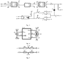
- Fig. 3 is a schematic diagram of a gate detection circuit of an insulated gate bipolar transistor according to an embodiment of the present application. As shown in Fig. 3 : S+ and S- are the input signals of the PWM of the driver board.
- U1 is the isolation optocoupler of the optocoupler isolation circuit 4, which plays the role of signal isolation and can be connected to the power supply, such as the positive power supply of +15V and the negative power supply of -5V.
- Resistor R1 is the current limiting resistor on the input side of the isolation optocoupler U1.
- U2 is the pulse shaper of the pulse shaping circuit 1, which shapes the output signal of the isolation optocoupler U1 into a square wave, and outputs two complementary signals PH and PL.
- U3 is a push-pull driver of the pulse amplification circuit 5, which can amplify the PH signal for driving the insulated gate bipolar transistor to be turned on.
- Resistor Rg is the gate resistor of the insulated gate bipolar transistor.
- G is connected to the gate G of the insulated gate bipolar transistor
- VE is connected to the emitter E of the insulated gate bipolar transistor
- the resistor Rge is an anti-open circuit resistor connected in parallel between the G and E terminals of the insulated gate bipolar transistor.
- Diode D1 and a resistor R3 constitute the detection power supply circuit 7.
- the cathode of the diode D1 is connected to the gate of the insulated gate bipolar transistor, the anode is connected to the comparator circuit 2, one end of the resistor R3 is connected to the anode of the diode D1, and the other end is connected to the positive power output terminal of the power supply, a positive power supply such as +15V.
- a first triode Q1, a second triode Q2, a first comparator U6, and the second comparator U7 consist of the comparison circuit 2.
- the first triode Q1 is configured to be turned on when the first square wave signal PH is at the high level
- the second triode Q2 is configured to be turned on when the second square wave signal PL is at the high level
- the first comparator U6 is connected to the first triode Q1, and configured for comparing the first preset voltage (eg 7.5V) with the voltage of the gate of the insulated gate bipolar transistor when the first triode Q1 is turned on, and outputting the low level when the first preset voltage is greater than the voltage of the gate of the insulated gate bipolar transistor, outputting the high level the first preset voltage is less than the voltage of the gate of the insulated gate bipolar transistor
- the second comparator U7 is connected to the second triode Q2, and is configured for comparing the second preset voltage (eg -2.5V) with the voltage of the gate of the insulated gate bipolar transistor when the second
- U5 is the common optocoupler of the fault output circuit 3, which can be connected to the positive power supply of +15V
- the resistor R2 is the current limiting resistor of the optocoupler U5.
- Fig. 4 is a schematic diagram of a power supply provided by an embodiment of the present application.
- U4 is the power supply
- the power supply can output a positive power supply of +15V and a negative power supply of -5V
- Capacitors C1-C3 are filter capacitors of the power supply, and the VE terminal is connected to the emitter E of the insulated gate bipolar transistor.
- Fig. 5 is a schematic diagram of a voltage division circuit provided by an embodiment of the present application.
- the voltage division circuit 6 receives the positive power supply of +15V and the negative power supply of -5V output by the power supply, and divides the voltage through R4-R7 to output the first preset voltages of +7.5V and the second preset voltage of -2.5V to the comparison circuit 2.
- the VE terminal is connected to the emitter E of the insulated gate bipolar transistor.
- the isolation optocoupler U1 When the PWM input signal is at the high level, the isolation optocoupler U1 is turned on, the first square wave signal PH is 1 (high level), the second square wave signal PL is 0 (low level), the gate voltage of the insulated gate bipolar transistor is normally 15V, the first triode Q1 is turned on, the second triode Q2 is turned off, the pin-5 of the first comparator U6 is 15V, the first preset voltage is 7.5V which is less than 15V, the pin-1 output of the first comparator U6 is at the high level, the pin-1 output of the second comparator U7 is shielded, the optocoupler U5 is turned off, and no fault signal is output; at this time, if the gate of the insulated gate bipolar transistor breaks down, the gate voltage of the insulated gate bipolar transistor is reduced to VE (0V), then the pin-5 of the first comparator U6 is 0V which is less than the first preset voltage of 7.5V, and the pin-1 output of the first comparator U
- the isolation optocoupler U1 When the PWM input signal is at the low level, the isolation optocoupler U1 is turned off, the first square wave signal PH is 0 (low level), the second square wave signal PL is 1 (high level), and the gate voltage of the insulated gate bipolar transistor is normally -5V, the first triode Q1 is turned off, the second triode Q2 is turned on, the pin-4 of the first comparator U6 is -5V, which is lower than second preset voltage of -2.5V, the pin-1 output of the comparator U7 is the high level, the pin-1 output of the first comparator U6 is shielded, the optocoupler U5 is turned off, and no fault signal is output; at this time, if the gate of the insulated gate bipolar transistor breaks down, the gate voltage of the insulated gate bipolar transistor is raised to VE (0V), the pin-4 of the second comparator U7 is 0V, which is greater than the second preset voltage of -2.5V, and the pin-1 output of the second comparator U
- the gate fault detection circuit of the insulated gate bipolar transistor of the present application can detect the gate of the insulated gate bipolar transistor in real time regardless of whether the insulated gate bipolar transistor is turned on or off after the gate of the insulated gate bipolar transistor is broken down failure, so that detects such as shutdown can be taken in time to avoid damage to other insulated gate bipolar transistors.
- the present application also provides a method for gate detection of an insulated gate bipolar transistor, the method includes: shaping a input signal of a signal input device through a pulse shaping circuit, and outputting a first square wave signal of a high level and a second square wave signal of a low level when the input signal is at the high level; and outputting a first square wave signal of the low level and a second square wave signal of the high level when the input signal is at the low level; comparing, through a comparison circuit, a first preset voltage with a voltage of a gate of the insulated gate bipolar transistor when the first square wave signal is at the high level, and outputting a low level when the first preset voltage is greater than the voltage of the gate of the insulated gate bipolar transistor; and comparing, through the comparison circuit, a second preset voltage with a voltage of a gate of the insulated gate bipolar transistor when the second square wave signal is at the high level, and outputting a low level when the second preset voltage is lower than the voltage of the gate of the insulated gate
- the method further includes: outputting the high level when the first preset voltage is lower than the voltage of the gate of the insulated gate bipolar transistor in a case that the first square wave signal is at the high level; and outputting the high level when the second preset voltage is greater than the voltage of the gate of the insulated gate bipolar transistor in a case that the second square wave signal is at the high level.
- the present application also provides an electric vehicle including the gate detection circuit of the insulated gate bipolar transistor described above.
Landscapes
- Physics & Mathematics (AREA)
- General Physics & Mathematics (AREA)
- Engineering & Computer Science (AREA)
- Microelectronics & Electronic Packaging (AREA)
- Electronic Switches (AREA)
- Power Conversion In General (AREA)
- Testing Of Individual Semiconductor Devices (AREA)
Abstract
Description
- The present application claims priority of
Chinese Invention Patent application, with Application No. 201911190671.8, filed on November 28, 2019 - The present application relates to the technical field of electronic circuits, and more particularly to a gate detection circuit of an insulated gate bipolar transistor.
- The insulated gate bipolar transistor (IGBT) is a composite fully-controlled voltage-driven power semiconductor device composed of a bipolar triode and an insulated gate field effect transistor. The units of the IGBT configured for driving are provided with multiple IGBTs, and when one of the gates breaks down, other IGBTs may also be damaged. However, there is currently no technology to detect IGBT gate faults.
- In view of this, the present application aims to provide a gate detection circuit of an insulated gate bipolar transistor to detect the gate fault of the insulated gate bipolar transistor.
- In order to achieve the above-mentioned object, the technical scheme of the present application is realized as follows:
- A gate detection circuit of an insulated gate bipolar transistor, and the gate detection circuit includes: a pulse shaping circuit, a comparison circuit, and a fault output circuit; the pulse shaping circuit is configured for shaping an input signal of a signal input device, and outputting a first square wave signal of a high level and a second square wave signal of a low level when the input signal is at the high level; and outputting a first square wave signal of the low level and a second square wave signal of the high level when the input signal is at the low level; the comparison circuit is configured for: comparing a first preset voltage with a voltage of a gate of the insulated gate bipolar transistor when the first square wave signal is at the high level, and outputting a low level when the first preset voltage is greater than the voltage of the gate of the insulated gate bipolar transistor; and comparing a second preset voltage with a voltage of a gate of the insulated gate bipolar transistor when the second square wave signal is at the high level, and outputting a low level when the second preset voltage is lower than the voltage of the gate of the insulated gate bipolar transistor; and the fault output circuit is configured for outputting a gate fault signal when the comparison circuit outputs the low level.
- Further, the comparison circuit includes: a first triode, configured to be turned on when the first square wave signal is at the high level; a second triode, configured to be turned on when the second square wave signal is at the high level; a first comparator, connected to the first triode and configured for comparing the first preset voltage with the voltage of the gate of the insulated gate bipolar transistor when the first triode is turned on; and a second comparator, connected to the second triode and configured for comparing the second preset voltage with the voltage of the gate of the insulated gate bipolar transistor when the second triode is turned on.
- Further, the gate detection circuit further includes: an optocoupler isolation circuit, connected between the signal input device and the pulse shaping circuit, and configured for optoelectronic isolation of the input signal.
- Further, the gate detection circuit further includes: a pulse amplification circuit, connected between the pulse shaping circuit and the insulated gate bipolar transistor, and configured for amplifying the first square wave signal to drive the insulated gate bipolar transistor.
- Further, the gate detection circuit further includes: a voltage division circuit, connected to the comparison circuit, and configured for converting a voltage of a power supply into the first preset voltage and the second preset voltage.
- Further, the gate detection circuit further includes: a detection power supply circuit, including:
- a diode, with a negative electrode being connected to the gate of the insulated gate bipolar transistor, and a positive electrode being connected to the comparison circuit; and
- a first resistor, with an end being connected to an anode of the diode, and the other end being connected to ta positive power output terminal of a power supply.
- Further, the power supply outputs a positive power supply of +15V and a negative power supply of -5V
- Further, the first preset voltage is 7.5V, and the second preset voltage is -2.5V
- Further, the comparison circuit is further configured for: outputting the high level when the first preset voltage is lower than the voltage of the gate of the insulated gate bipolar transistor in a case that the first square wave signal is at the high level; and outputting the high level when the second preset voltage is greater than the voltage of the gate of the insulated gate bipolar transistor in a case that the second square wave signal is at the high level.
- Further, the fault output circuit is further configured to not output a fault signal when the comparator circuit outputs the high level.
- Compared to the prior art, the gate detection circuit of the insulated gate bipolar transistor described in the present application has the following advantages:
- Using the pulse shaping circuit, the comparison circuit, and the fault output circuit, and the pulse shaping circuit is configured to output the first square wave signal of the high/low level and the second square wave signal of the high/low level; and using the comparison circuit to compare the first preset voltage with the voltage of the gate of the insulated gate bipolar transistor, or compare the second preset voltage with the voltage of the gate of the insulated gate bipolar transistor, and to output the low level when the first preset voltage is greater than the voltage of the gate of the insulated gate bipolar transistor or the second preset voltage is lower than the voltage of the gate of the insulated gate bipolar transistor; and finally, the fault output circuit outputs a gate fault signal when the comparison circuit outputs the low level; therefore, the gate fault of the insulated gate bipolar transistor can be detected.
- The present application further provides a method for gate detection of an insulated gate bipolar transistor, to detect the gate fault of the insulated gate bipolar transistor.
- In order to achieve the above-mentioned object, the technical scheme of the present application is realized as follows:
- A method for gate detection of an insulated gate bipolar transistor, and the method includes:
- shaping a input signal of a signal input device through a pulse shaping circuit, and outputting a first square wave signal of a high level and a second square wave signal of a low level when the input signal is at the high level; and outputting a first square wave signal of the low level and a second square wave signal of the high level when the input signal is at the low level; comparing, through a comparison circuit, a first preset voltage with a voltage of a gate of the insulated gate bipolar transistor when the first square wave signal is at the high level, and outputting a low level when the first preset voltage is greater than the voltage of the gate of the insulated gate bipolar transistor; and
- comparing, through the comparison circuit, a second preset voltage with a voltage of a gate of the insulated gate bipolar transistor when the second square wave signal is at the high level, and
- outputting a low level when the second preset voltage is lower than the voltage of the gate of the insulated gate bipolar transistor; and outputting, through a fault output circuit, a gate fault signal when the comparison circuit outputs the low level.
- Further, the method further includes: outputting the high level when the first preset voltage is lower than the voltage of the gate of the insulated gate bipolar transistor in a case that the first square wave signal is at the high level; and outputting the high level when the second preset voltage is greater than the voltage of the gate of the insulated gate bipolar transistor in a case that the second square wave signal is at the high level.
- The advantages of the method for gate detection of the insulated gate bipolar transistor described above are similar to those of the gate detection circuit of the insulated gate bipolar transistor described above, and will not be repeated herein.
- The present application further provides an electric vehicle, to detect the gate fault of the insulated gate bipolar transistor.
- In order to achieve the above-mentioned object, the technical scheme of the present application is realized as follows:
- An electric vehicle, and the electric vehicle includes the gate detection circuit of an insulated gate bipolar transistor described above.
- The advantages of the electric vehicle described above are similar to those of the gate detection circuit of the insulated gate bipolar transistor described above, and will not be repeated herein.
- Other features and advantages of the present application will be described in detail in the detailed description that follows.
- The accompanying drawings constituting a part of the present application are used to provide further understanding of the present application, and the schematic embodiments of the present application and descriptions thereof are used to explain the present application and do not constitute an improper limitation of the present application. In the drawings:
-
Fig. 1 is a structural block diagram of a gate detection circuit of an insulated gate bipolar transistor provided by an embodiment of the present application; -
Fig. 2 is a structural block diagram of a gate detection circuit of an insulated gate bipolar transistor provided by another embodiment of the present application; -
Fig. 3 is a schematic diagram of a gate detection circuit of an insulated gate bipolar transistor provided by an embodiment of the present application; -
Fig. 4 is a schematic diagram of a power supply provided by an embodiment of the present application; and -
Fig. 5 is a schematic diagram of a voltage division circuit provided by an embodiment of the present application. - The reference numerals are listed as following:
- 1- pulse shaping circuit; 2-comparison circuit;
- 2- fault output circuit, 4-optocoupler isolation circuit;
- 5-pulse amplification circuit; 6-voltage division circuit; and
- 7-detection power supply circuit.
- It should be noted that the embodiments of the present application and the features of the embodiments may be combined with each other unless there is conflict.
- The present application will be described in detail below with reference to the accompanying drawings and in conjunction with the embodiments.
-
Fig. 1 is a structural block diagram of a gate detection circuit of an insulated gate bipolar transistor according to an embodiment of the present application. As shown inFig.1 , the circuit includes: apulse shaping circuit 1, acomparison circuit 2, and afault output circuit 3. - The
pulse shaping circuit 1 is configured for shaping an input signal of a signal input device, and outputting a first square wave signal of a high level and a second square wave signal of a low level when the input signal is at the high level; and outputting a first square wave signal of the low level and a second square wave signal of the high level when the input signal is at the low level. - Specifically, the signal input device is, for example, a motor drive controller of an electric vehicle, and the input signal is, for example, a pulse width modulation (PWM) signal of a drive board, but is not limited thereto. The
pulse shaping circuit 1 can shape the input signal into a square wave, and output the complementary first square wave signal and the second square wave signal in different level states according to the different level states of the input signal, and the level states of the first square wave signal and the second square wave signal may affect which preset voltage thecomparison circuit 2 uses for comparison. - The
comparison circuit 2 is configured for: comparing a first preset voltage with a voltage of a gate of the insulated gate bipolar transistor when the first square wave signal is at the high level, and outputting a low level when the first preset voltage is greater than the voltage of the gate of the insulated gate bipolar transistor; and comparing a second preset voltage with a voltage of a gate of the insulated gate bipolar transistor when the second square wave signal is at the high level, and outputting a low level when the second preset voltage is lower than the voltage of the gate of the insulated gate bipolar transistor. - Specifically, the
comparison circuit 2 can use two preset voltages to compare with the voltage of the gate of the insulated gate bipolar transistor, since the level state of the input signal varies with the signal input device, the normal insulated gate bipolar transistor will also have two states of on and off, so that the voltage of the gate will also be different. For example, assuming that under the action of an external power supply with 15V, when the input signal is at high level, the voltage of the gate of the insulated gate bipolar transistor can be 15V, and when the input signal is at low level, the voltage of the gate of the insulated gate bipolar transistor may be -5V. In addition, when the gate of the insulated gate bipolar transistor fails, the voltage of the gate of the insulated gate bipolar transistor is 0V. In this regard, the first preset voltage can be set to 7.5V, and the second preset voltage can be set to -2.5V, so as to effectively determine that the insulated gate bipolar transistor will have gate faults in both on and off states. It can be understood that the above data is only an example (the same below), which is not limited in the present application. For example, the first preset voltage may be a voltage greater than 0 and less than 15V, and the second preset voltage may also be a voltage greater than -5V and less than -2.5V - The
fault output circuit 3 is configured to output a gate fault signal when thecomparison circuit 2 outputs the low level. - Specifically, the gate fault in the embodiments of the present application is, for example, gate breakdown. The
fault output circuit 3 outputs the gate fault signal to the signal input device when thecomparator circuit 2 outputs the low level. -
FIG. 2 is a structural block diagram of a gate detection circuit of an insulated gate bipolar transistor according to another embodiment of the present application. As shown inFig. 2 , the circuit further includes: - an
optocoupler isolation circuit 4, connected between the signal input device and thepulse shaping circuit 1, and configured for optoelectronic isolation of the input signal. - a
pulse amplification circuit 5, connected between thepulse shaping circuit 1 and the insulated gate bipolar transistor, and configured for amplifying the first square wave signal to drive the insulated gate bipolar transistor. - a
voltage division circuit 6, connected to thecomparison circuit 2, and configured for converting a voltage of a power supply into the first preset voltage and the second preset voltage. - a detection
power supply circuit 7, connected to thecomparison circuit 2 and the gate of the insulated gate bipolar transistor, and configured for providing an external power supply to thecomparison circuit 2 and the gate of the insulated gate bipolar transistor. - More specific functions of the above-mentioned parts will be detailed below through detailed circuit components.
-
Fig. 3 is a schematic diagram of a gate detection circuit of an insulated gate bipolar transistor according to an embodiment of the present application. As shown inFig. 3 :
S+ and S- are the input signals of the PWM of the driver board. - U1 is the isolation optocoupler of the
optocoupler isolation circuit 4, which plays the role of signal isolation and can be connected to the power supply, such as the positive power supply of +15V and the negative power supply of -5V. Resistor R1 is the current limiting resistor on the input side of the isolation optocoupler U1. - U2 is the pulse shaper of the
pulse shaping circuit 1, which shapes the output signal of the isolation optocoupler U1 into a square wave, and outputs two complementary signals PH and PL. - U3 is a push-pull driver of the
pulse amplification circuit 5, which can amplify the PH signal for driving the insulated gate bipolar transistor to be turned on. - Resistor Rg is the gate resistor of the insulated gate bipolar transistor. In the figure, G is connected to the gate G of the insulated gate bipolar transistor, VE is connected to the emitter E of the insulated gate bipolar transistor, and the resistor Rge is an anti-open circuit resistor connected in parallel between the G and E terminals of the insulated gate bipolar transistor.
- Diode D1 and a resistor R3 constitute the detection
power supply circuit 7. The cathode of the diode D1 is connected to the gate of the insulated gate bipolar transistor, the anode is connected to thecomparator circuit 2, one end of the resistor R3 is connected to the anode of the diode D1, and the other end is connected to the positive power output terminal of the power supply, a positive power supply such as +15V. - A first triode Q1, a second triode Q2, a first comparator U6, and the second comparator U7 consist of the
comparison circuit 2. Among them, the first triode Q1 is configured to be turned on when the first square wave signal PH is at the high level; the second triode Q2 is configured to be turned on when the second square wave signal PL is at the high level; the first comparator U6 is connected to the first triode Q1, and configured for comparing the first preset voltage (eg 7.5V) with the voltage of the gate of the insulated gate bipolar transistor when the first triode Q1 is turned on, and outputting the low level when the first preset voltage is greater than the voltage of the gate of the insulated gate bipolar transistor, outputting the high level the first preset voltage is less than the voltage of the gate of the insulated gate bipolar transistor; the second comparator U7 is connected to the second triode Q2, and is configured for comparing the second preset voltage (eg -2.5V) with the voltage of the gate of the insulated gate bipolar transistor when the second triode Q2 is turned on, and outputting the low level when the second preset voltage is lower than the voltage of the gate of the insulated gate bipolar transistor, outputting the high level the second preset voltage is greater than the voltage of the gate of the insulated gate bipolar transistor. - U5 is the common optocoupler of the
fault output circuit 3, which can be connected to the positive power supply of +15V The resistor R2 is the current limiting resistor of the optocoupler U5. When thecomparator circuit 2 outputs the low level, the gate fault signals GZ+ and GZ- are output. -
Fig. 4 is a schematic diagram of a power supply provided by an embodiment of the present application. As shown inFig. 4 , U4 is the power supply, and the power supply can output a positive power supply of +15V and a negative power supply of -5V Capacitors C1-C3 are filter capacitors of the power supply, and the VE terminal is connected to the emitter E of the insulated gate bipolar transistor. -
Fig. 5 is a schematic diagram of a voltage division circuit provided by an embodiment of the present application. As shown inFig. 5 , thevoltage division circuit 6 receives the positive power supply of +15V and the negative power supply of -5V output by the power supply, and divides the voltage through R4-R7 to output the first preset voltages of +7.5V and the second preset voltage of -2.5V to thecomparison circuit 2. Similarly, the VE terminal is connected to the emitter E of the insulated gate bipolar transistor. - The working process of the gate detection circuit of the insulated gate bipolar transistor of the present application is described in detail below:
- When the PWM input signal is at the high level, the isolation optocoupler U1 is turned on, the first square wave signal PH is 1 (high level), the second square wave signal PL is 0 (low level), the gate voltage of the insulated gate bipolar transistor is normally 15V, the first triode Q1 is turned on, the second triode Q2 is turned off, the pin-5 of the first comparator U6 is 15V, the first preset voltage is 7.5V which is less than 15V, the pin-1 output of the first comparator U6 is at the high level, the pin-1 output of the second comparator U7 is shielded, the optocoupler U5 is turned off, and no fault signal is output; at this time, if the gate of the insulated gate bipolar transistor breaks down, the gate voltage of the insulated gate bipolar transistor is reduced to VE (0V), then the pin-5 of the first comparator U6 is 0V which is less than the first preset voltage of 7.5V, and the pin-1 output of the first comparator U6 is at the low level, the optocoupler U5 is turned on, and the fault signal is output.
- When the PWM input signal is at the low level, the isolation optocoupler U1 is turned off, the first square wave signal PH is 0 (low level), the second square wave signal PL is 1 (high level), and the gate voltage of the insulated gate bipolar transistor is normally -5V, the first triode Q1 is turned off, the second triode Q2 is turned on, the pin-4 of the first comparator U6 is -5V, which is lower than second preset voltage of -2.5V, the pin-1 output of the comparator U7 is the high level, the pin-1 output of the first comparator U6 is shielded, the optocoupler U5 is turned off, and no fault signal is output; at this time, if the gate of the insulated gate bipolar transistor breaks down, the gate voltage of the insulated gate bipolar transistor is raised to VE (0V), the pin-4 of the second comparator U7 is 0V, which is greater than the second preset voltage of -2.5V, and the pin-1 output of the second comparator U7 is the low level, the optocoupler U5 is turned on, and a fault signal is output.
- The gate fault detection circuit of the insulated gate bipolar transistor of the present application can detect the gate of the insulated gate bipolar transistor in real time regardless of whether the insulated gate bipolar transistor is turned on or off after the gate of the insulated gate bipolar transistor is broken down failure, so that detects such as shutdown can be taken in time to avoid damage to other insulated gate bipolar transistors.
- The present application also provides a method for gate detection of an insulated gate bipolar transistor, the method includes: shaping a input signal of a signal input device through a pulse shaping circuit, and outputting a first square wave signal of a high level and a second square wave signal of a low level when the input signal is at the high level; and outputting a first square wave signal of the low level and a second square wave signal of the high level when the input signal is at the low level; comparing, through a comparison circuit, a first preset voltage with a voltage of a gate of the insulated gate bipolar transistor when the first square wave signal is at the high level, and outputting a low level when the first preset voltage is greater than the voltage of the gate of the insulated gate bipolar transistor; and comparing, through the comparison circuit, a second preset voltage with a voltage of a gate of the insulated gate bipolar transistor when the second square wave signal is at the high level, and outputting a low level when the second preset voltage is lower than the voltage of the gate of the insulated gate bipolar transistor; and outputting, through a fault output circuit, a gate fault signal when the comparison circuit outputs the low level.
- Further, the method further includes: outputting the high level when the first preset voltage is lower than the voltage of the gate of the insulated gate bipolar transistor in a case that the first square wave signal is at the high level; and outputting the high level when the second preset voltage is greater than the voltage of the gate of the insulated gate bipolar transistor in a case that the second square wave signal is at the high level.
- The present application also provides an electric vehicle including the gate detection circuit of the insulated gate bipolar transistor described above.
- The above descriptions are only preferred embodiments of the present application, and are not intended to limit the present application. Any modifications, equivalent replacements, improvements, etc. made within the principles of the present application shall be included within the protection scope of the present application.
Claims (13)
- A gate detection circuit of an insulated gate bipolar transistor, wherein the gate detection circuit comprises:a pulse shaping circuit, configured for shaping an input signal of a signal input device, andoutputting a first square wave signal of a high level and a second square wave signal of a low level when the input signal is at the high level; andoutputting a first square wave signal of the low level and a second square wave signal of the high level when the input signal is at the low level;a comparison circuit, configured for:comparing a first preset voltage with a voltage of a gate of the insulated gate bipolar transistor when the first square wave signal is at the high level, and outputting a low level when the first preset voltage is greater than the voltage of the gate of the insulated gate bipolar transistor; andcomparing a second preset voltage with a voltage of a gate of the insulated gate bipolar transistor when the second square wave signal is at the high level, and outputting a low level when the second preset voltage is lower than the voltage of the gate of the insulated gate bipolar transistor; anda fault output circuit, configured for outputting a gate fault signal when the comparison circuit outputs the low level.
- The gate detection circuit of an insulated gate bipolar transistor according to claim 1, wherein the comparison circuit comprises:a first triode, configured to be turned on when the first square wave signal is at the high level;a second triode, configured to be turned on when the second square wave signal is at the high level;a first comparator, connected to the first triode and configured for comparing the first preset voltage with the voltage of the gate of the insulated gate bipolar transistor when the first triode is turned on; anda second comparator, connected to the second triode and configured for comparing the second preset voltage with the voltage of the gate of the insulated gate bipolar transistor when the second triode is turned on.
- The gate detection circuit of an insulated gate bipolar transistor according to claim 1, wherein the gate detection circuit further comprises:an optocoupler isolation circuit, connected between the signal input device and the pulse shaping circuit,and configured for optoelectronic isolation of the input signal.
- The gate detection circuit of an insulated gate bipolar transistor according to claim 1, wherein the gate detection circuit further comprises:
a pulse amplification circuit, connected between the pulse shaping circuit and the insulated gate bipolar transistor, and configured for amplifying the first square wave signal to drive the insulated gate bipolar transistor. - The gate detection circuit of an insulated gate bipolar transistor according to claim 1, wherein the gate detection circuit further comprises:
a voltage division circuit, connected to the comparison circuit, and configured for converting a voltage of a power supply into the first preset voltage and the second preset voltage. - The gate detection circuit of an insulated gate bipolar transistor according to claim 1, wherein the gate detection circuit further comprises:
a detection power supply circuit, comprising:a diode, with a negative electrode being connected to the gate of the insulated gate bipolar transistor, anda positive electrode being connected to the comparison circuit; anda first resistor, with an end being connected to an anode of the diode, and the other end being connected to ta positive power output terminal of a power supply. - The gate detection circuit of an insulated gate bipolar transistor according to claim 5 or 6, wherein the power supply outputs a positive power supply of +15V and a negative power supply of -5V.
- The gate detection circuit of an insulated gate bipolar transistor according to claim 1, wherein the first preset voltage is 7.5V, and the second preset voltage is -2.5V
- The gate detection circuit of an insulated gate bipolar transistor according to claim 1, wherein the comparison circuit is further configured for:outputting the high level when the first preset voltage is lower than the voltage of the gate of the insulated gate bipolar transistor in a case that the first square wave signal is at the high level; andoutputting the high level when the second preset voltage is greater than the voltage of the gate of the insulated gate bipolar transistor in a case that the second square wave signal is at the high level.
- The gate detection circuit of an insulated gate bipolar transistor according to claim 1, wherein the fault output circuit is further configured to not output a fault signal when the comparator circuit outputs the high level.
- A method for gate detection of an insulated gate bipolar transistor, comprising:shaping a input signal of a signal input device through a pulse shaping circuit, and outputting a first square wave signal of a high level and a second square wave signal of a low level when the input signal is at the high level; and outputting a first square wave signal of the low level and a second square wave signal of the high level when the input signal is at the low level;comparing, through a comparison circuit, a first preset voltage with a voltage of a gate of the insulated gate bipolar transistor when the first square wave signal is at the high level, and outputting a low level when the first preset voltage is greater than the voltage of the gate of the insulated gate bipolar transistor;and comparing, through the comparison circuit, a second preset voltage with a voltage of a gate of the insulated gate bipolar transistor when the second square wave signal is at the high level, and outputting a low level when the second preset voltage is lower than the voltage of the gate of the insulated gate bipolar transistor; andoutputting, through a fault output circuit, a gate fault signal when the comparison circuit outputs the low level.
- The method for gate detection of an insulated gate bipolar transistor according to claim 11, wherein the method further comprises:outputting the high level when the first preset voltage is lower than the voltage of the gate of the insulated gate bipolar transistor in a case that the first square wave signal is at the high level; andoutputting the high level when the second preset voltage is greater than the voltage of the gate of the insulated gate bipolar transistor in a case that the second square wave signal is at the high level.
- An electric vehicle, comprising the gate detection circuit of an insulated gate bipolar transistor according to any one of claims 1-10.
Applications Claiming Priority (2)
| Application Number | Priority Date | Filing Date | Title |
|---|---|---|---|
| CN201911190671.8A CN112051494B (en) | 2019-11-28 | 2019-11-28 | Gate Detection Circuit of Insulated Gate Bipolar Transistor |
| PCT/CN2020/131427 WO2021104297A1 (en) | 2019-11-28 | 2020-11-25 | Gate detection circuit of insulated gate bipolar transistor |
Publications (3)
| Publication Number | Publication Date |
|---|---|
| EP4024064A1 true EP4024064A1 (en) | 2022-07-06 |
| EP4024064A4 EP4024064A4 (en) | 2022-10-19 |
| EP4024064B1 EP4024064B1 (en) | 2025-07-30 |
Family
ID=73609041
Family Applications (1)
| Application Number | Title | Priority Date | Filing Date |
|---|---|---|---|
| EP20894755.6A Active EP4024064B1 (en) | 2019-11-28 | 2020-11-25 | Gate fault detection circuit of insulated gate bipolar transistor |
Country Status (6)
| Country | Link |
|---|---|
| US (1) | US12019115B2 (en) |
| EP (1) | EP4024064B1 (en) |
| JP (1) | JP7307275B2 (en) |
| KR (1) | KR102827409B1 (en) |
| CN (1) | CN112051494B (en) |
| WO (1) | WO2021104297A1 (en) |
Families Citing this family (2)
| Publication number | Priority date | Publication date | Assignee | Title |
|---|---|---|---|---|
| CN113447790B (en) * | 2021-07-13 | 2022-10-25 | 西安交通大学 | Non-contact IGBT state monitoring device |
| CN115032518B (en) * | 2022-08-11 | 2022-11-15 | 佛山市联动科技股份有限公司 | Dynamic threshold voltage testing device and method |
Family Cites Families (23)
| Publication number | Priority date | Publication date | Assignee | Title |
|---|---|---|---|---|
| US4500838A (en) * | 1983-01-24 | 1985-02-19 | General Electric Company | Current sensor |
| US6809515B1 (en) | 1998-07-31 | 2004-10-26 | Spinix Corporation | Passive solid-state magnetic field sensors and applications therefor |
| JP2002095240A (en) * | 2000-09-18 | 2002-03-29 | Toshiba Corp | Gate drive circuit for insulated gate semiconductor device and power converter using the same |
| JP5315155B2 (en) * | 2009-07-23 | 2013-10-16 | 日立オートモティブシステムズ株式会社 | Semiconductor element control device, automotive electrical system |
| CN102324918B (en) * | 2011-06-09 | 2013-06-26 | 深圳市英威腾电气股份有限公司 | IGBT (insulated gate bipolar transistor) drive circuit |
| CN102510276B (en) | 2011-11-01 | 2013-09-25 | 华南理工大学 | Big-power module high-frequency driver with non-neural advance mechanism |
| CN103199832B (en) | 2012-01-06 | 2015-11-25 | 中国北车股份有限公司 | IGBT Drive Protecting Circuit and system |
| CN103427809B (en) * | 2012-05-21 | 2016-04-20 | 永济新时速电机电器有限责任公司 | The protective circuit of insulated gate bipolar transistor |
| CN104237761B (en) * | 2013-06-13 | 2018-05-04 | 通用电气公司 | The system and method for the failure mode detection and protection of insulated gate bipolar transistor |
| KR101769650B1 (en) * | 2013-12-18 | 2017-08-30 | 엘에스산전 주식회사 | circuit of checking IGBT Module failure through monitoring the gate voltage |
| CN204013200U (en) | 2014-09-03 | 2014-12-10 | 湘潭电机股份有限公司 | One is applicable to three-level current transformer IGBT drive circuit |
| CN204119014U (en) * | 2014-11-03 | 2015-01-21 | 哈尔滨同为电气股份有限公司 | A three-level IGBT drive and protection circuit |
| CN104935315B (en) * | 2015-07-15 | 2019-02-19 | 北京京东方能源科技有限公司 | IGBT drive circuit |
| JP6748935B2 (en) * | 2015-09-04 | 2020-09-02 | 富士電機株式会社 | Protection circuit for semiconductor switch with current sense |
| US10254327B2 (en) | 2016-02-29 | 2019-04-09 | Infineon Technologies Ag | Method and device for short circuit detection in power semiconductor switches |
| US10840430B2 (en) * | 2016-06-30 | 2020-11-17 | Intel Corporation | Piezoelectric package-integrated sensing devices |
| CN106099864B (en) * | 2016-07-19 | 2018-04-24 | 东南大学 | A kind of short-circuit protection method and its circuit of IGBT device for power switching |
| JP6300964B1 (en) | 2017-01-13 | 2018-03-28 | 三菱電機株式会社 | Power converter |
| JP6355775B2 (en) | 2017-02-10 | 2018-07-11 | ルネサスエレクトロニクス株式会社 | Gate driver and switching method |
| CN107807319B (en) | 2017-09-22 | 2020-03-10 | 全球能源互联网研究院有限公司 | An insulated gate bipolar transistor IGBT test circuit and method |
| RU186888U1 (en) | 2018-07-30 | 2019-02-07 | Общество с ограниченной ответственностью "Газпром трансгаз Ухта" | TEST STAND FOR IGBT TRANSISTORS AND DRIVERS OF THEIR GATEWAYS |
| CN109061431B (en) * | 2018-08-22 | 2020-11-13 | 徐州中矿大传动与自动化有限公司 | Grid charge-based SiC MOSFET grid fault diagnosis system and diagnosis method |
| CN109375087B (en) * | 2018-10-11 | 2021-06-15 | 连云港杰瑞电子有限公司 | A protection circuit and method with high-speed detection of IGBT short-circuit fault |
-
2019
- 2019-11-28 CN CN201911190671.8A patent/CN112051494B/en active Active
-
2020
- 2020-11-25 WO PCT/CN2020/131427 patent/WO2021104297A1/en not_active Ceased
- 2020-11-25 US US17/765,577 patent/US12019115B2/en active Active
- 2020-11-25 KR KR1020227010697A patent/KR102827409B1/en active Active
- 2020-11-25 JP JP2022520292A patent/JP7307275B2/en active Active
- 2020-11-25 EP EP20894755.6A patent/EP4024064B1/en active Active
Also Published As
| Publication number | Publication date |
|---|---|
| US12019115B2 (en) | 2024-06-25 |
| EP4024064A4 (en) | 2022-10-19 |
| CN112051494B (en) | 2021-07-20 |
| KR102827409B1 (en) | 2025-07-01 |
| CN112051494A (en) | 2020-12-08 |
| JP7307275B2 (en) | 2023-07-11 |
| JP2022550950A (en) | 2022-12-06 |
| US20230160945A1 (en) | 2023-05-25 |
| EP4024064B1 (en) | 2025-07-30 |
| WO2021104297A1 (en) | 2021-06-03 |
| KR20220054856A (en) | 2022-05-03 |
Similar Documents
| Publication | Publication Date | Title |
|---|---|---|
| US9960766B2 (en) | Insulated gate bipolar transistor driving circuit | |
| CN103178694B (en) | Insulated gate bipolar transistor gate driving push-pull circuit | |
| CN106059548B (en) | Switch unit and power circuit | |
| EP4024064B1 (en) | Gate fault detection circuit of insulated gate bipolar transistor | |
| US10886912B2 (en) | Gate circuit and gate drive circuit for power semiconductor switch | |
| CN110492723A (en) | A kind of fuel cell car high speed air compressor inverter driving circuit | |
| US11831307B2 (en) | Power switch drive circuit and device | |
| CN210578247U (en) | Protection circuit and device | |
| CN106023897B (en) | AMOLED drive systems and AMOLED driving methods | |
| CN105634251B (en) | with multi-functional IGBT drive circuit | |
| US8416006B1 (en) | Electronic device with gate driver for high voltage level shifter | |
| CN112688683A (en) | Apparatus and method for preventing inductive load driving circuit from being damaged by back electromotive force | |
| US12021493B1 (en) | Driving circuit for a switching transistor and a driving device including the same | |
| CN215222156U (en) | Three-level IGBT driving and direct-connection protection circuit | |
| CN219013504U (en) | Solenoid valve drive circuit and equipment with solenoid valve | |
| US10270376B2 (en) | Fan driving circuit | |
| RU2790219C1 (en) | System and method for diagnosing the gate of a bipolar transistor with an insulated gate | |
| CN215120553U (en) | Driving circuit for IGBT | |
| CN205377797U (en) | Prevent direct power drive circuit | |
| CN113437856B (en) | IGBT driving circuit and control method | |
| CN117498847A (en) | Intelligent PFC module | |
| JP2015033198A (en) | Gate control circuit of semiconductor element for power | |
| US20180351344A1 (en) | Drive circuit | |
| CN223414619U (en) | Anti-reverse protection circuit capable of keeping low standby quiescent current | |
| CN215581093U (en) | Push-pull type driving device |
Legal Events
| Date | Code | Title | Description |
|---|---|---|---|
| STAA | Information on the status of an ep patent application or granted ep patent |
Free format text: STATUS: THE INTERNATIONAL PUBLICATION HAS BEEN MADE |
|
| PUAI | Public reference made under article 153(3) epc to a published international application that has entered the european phase |
Free format text: ORIGINAL CODE: 0009012 |
|
| STAA | Information on the status of an ep patent application or granted ep patent |
Free format text: STATUS: REQUEST FOR EXAMINATION WAS MADE |
|
| 17P | Request for examination filed |
Effective date: 20220329 |
|
| AK | Designated contracting states |
Kind code of ref document: A1 Designated state(s): AL AT BE BG CH CY CZ DE DK EE ES FI FR GB GR HR HU IE IS IT LI LT LU LV MC MK MT NL NO PL PT RO RS SE SI SK SM TR |
|
| A4 | Supplementary search report drawn up and despatched |
Effective date: 20220919 |
|
| RIC1 | Information provided on ipc code assigned before grant |
Ipc: G01R 31/26 20200101AFI20220913BHEP |
|
| DAV | Request for validation of the european patent (deleted) | ||
| DAX | Request for extension of the european patent (deleted) | ||
| STAA | Information on the status of an ep patent application or granted ep patent |
Free format text: STATUS: EXAMINATION IS IN PROGRESS |
|
| 17Q | First examination report despatched |
Effective date: 20240104 |
|
| GRAP | Despatch of communication of intention to grant a patent |
Free format text: ORIGINAL CODE: EPIDOSNIGR1 |
|
| STAA | Information on the status of an ep patent application or granted ep patent |
Free format text: STATUS: GRANT OF PATENT IS INTENDED |
|
| INTG | Intention to grant announced |
Effective date: 20250225 |
|
| GRAS | Grant fee paid |
Free format text: ORIGINAL CODE: EPIDOSNIGR3 |
|
| GRAA | (expected) grant |
Free format text: ORIGINAL CODE: 0009210 |
|
| STAA | Information on the status of an ep patent application or granted ep patent |
Free format text: STATUS: THE PATENT HAS BEEN GRANTED |
|
| AK | Designated contracting states |
Kind code of ref document: B1 Designated state(s): AL AT BE BG CH CY CZ DE DK EE ES FI FR GB GR HR HU IE IS IT LI LT LU LV MC MK MT NL NO PL PT RO RS SE SI SK SM TR |
|
| REG | Reference to a national code |
Ref country code: GB Ref legal event code: FG4D |
|
| REG | Reference to a national code |
Ref country code: CH Ref legal event code: EP |
|
| REG | Reference to a national code |
Ref country code: DE Ref legal event code: R096 Ref document number: 602020055673 Country of ref document: DE |
|
| REG | Reference to a national code |
Ref country code: IE Ref legal event code: FG4D |
|
| P01 | Opt-out of the competence of the unified patent court (upc) registered |
Free format text: CASE NUMBER: UPC_APP_7225_4024064/2025 Effective date: 20250916 |
|
| REG | Reference to a national code |
Ref country code: NL Ref legal event code: MP Effective date: 20250730 |
|
| REG | Reference to a national code |
Ref country code: AT Ref legal event code: MK05 Ref document number: 1819481 Country of ref document: AT Kind code of ref document: T Effective date: 20250730 |
|
| PG25 | Lapsed in a contracting state [announced via postgrant information from national office to epo] |
Ref country code: PT Free format text: LAPSE BECAUSE OF FAILURE TO SUBMIT A TRANSLATION OF THE DESCRIPTION OR TO PAY THE FEE WITHIN THE PRESCRIBED TIME-LIMIT Effective date: 20251202 |
|
| PG25 | Lapsed in a contracting state [announced via postgrant information from national office to epo] |
Ref country code: IS Free format text: LAPSE BECAUSE OF FAILURE TO SUBMIT A TRANSLATION OF THE DESCRIPTION OR TO PAY THE FEE WITHIN THE PRESCRIBED TIME-LIMIT Effective date: 20251130 |
|
| PGFP | Annual fee paid to national office [announced via postgrant information from national office to epo] |
Ref country code: DE Payment date: 20251117 Year of fee payment: 6 |
|
| PGFP | Annual fee paid to national office [announced via postgrant information from national office to epo] |
Ref country code: GB Payment date: 20251126 Year of fee payment: 6 |
|
| PG25 | Lapsed in a contracting state [announced via postgrant information from national office to epo] |
Ref country code: NO Free format text: LAPSE BECAUSE OF FAILURE TO SUBMIT A TRANSLATION OF THE DESCRIPTION OR TO PAY THE FEE WITHIN THE PRESCRIBED TIME-LIMIT Effective date: 20251030 |
|
| REG | Reference to a national code |
Ref country code: LT Ref legal event code: MG9D |
|
| PG25 | Lapsed in a contracting state [announced via postgrant information from national office to epo] |
Ref country code: AT Free format text: LAPSE BECAUSE OF FAILURE TO SUBMIT A TRANSLATION OF THE DESCRIPTION OR TO PAY THE FEE WITHIN THE PRESCRIBED TIME-LIMIT Effective date: 20250730 |
|
| PG25 | Lapsed in a contracting state [announced via postgrant information from national office to epo] |
Ref country code: FI Free format text: LAPSE BECAUSE OF FAILURE TO SUBMIT A TRANSLATION OF THE DESCRIPTION OR TO PAY THE FEE WITHIN THE PRESCRIBED TIME-LIMIT Effective date: 20250730 |
|
| PG25 | Lapsed in a contracting state [announced via postgrant information from national office to epo] |
Ref country code: HR Free format text: LAPSE BECAUSE OF FAILURE TO SUBMIT A TRANSLATION OF THE DESCRIPTION OR TO PAY THE FEE WITHIN THE PRESCRIBED TIME-LIMIT Effective date: 20250730 Ref country code: NL Free format text: LAPSE BECAUSE OF FAILURE TO SUBMIT A TRANSLATION OF THE DESCRIPTION OR TO PAY THE FEE WITHIN THE PRESCRIBED TIME-LIMIT Effective date: 20250730 |
|
| PGFP | Annual fee paid to national office [announced via postgrant information from national office to epo] |
Ref country code: FR Payment date: 20251127 Year of fee payment: 6 |
|
| PG25 | Lapsed in a contracting state [announced via postgrant information from national office to epo] |
Ref country code: GR Free format text: LAPSE BECAUSE OF FAILURE TO SUBMIT A TRANSLATION OF THE DESCRIPTION OR TO PAY THE FEE WITHIN THE PRESCRIBED TIME-LIMIT Effective date: 20251031 |
|
| PG25 | Lapsed in a contracting state [announced via postgrant information from national office to epo] |
Ref country code: SE Free format text: LAPSE BECAUSE OF FAILURE TO SUBMIT A TRANSLATION OF THE DESCRIPTION OR TO PAY THE FEE WITHIN THE PRESCRIBED TIME-LIMIT Effective date: 20250730 |
|
| PG25 | Lapsed in a contracting state [announced via postgrant information from national office to epo] |
Ref country code: LV Free format text: LAPSE BECAUSE OF FAILURE TO SUBMIT A TRANSLATION OF THE DESCRIPTION OR TO PAY THE FEE WITHIN THE PRESCRIBED TIME-LIMIT Effective date: 20250730 |
|
| PG25 | Lapsed in a contracting state [announced via postgrant information from national office to epo] |
Ref country code: BG Free format text: LAPSE BECAUSE OF FAILURE TO SUBMIT A TRANSLATION OF THE DESCRIPTION OR TO PAY THE FEE WITHIN THE PRESCRIBED TIME-LIMIT Effective date: 20250730 Ref country code: PL Free format text: LAPSE BECAUSE OF FAILURE TO SUBMIT A TRANSLATION OF THE DESCRIPTION OR TO PAY THE FEE WITHIN THE PRESCRIBED TIME-LIMIT Effective date: 20250730 |
|
| PG25 | Lapsed in a contracting state [announced via postgrant information from national office to epo] |
Ref country code: RS Free format text: LAPSE BECAUSE OF FAILURE TO SUBMIT A TRANSLATION OF THE DESCRIPTION OR TO PAY THE FEE WITHIN THE PRESCRIBED TIME-LIMIT Effective date: 20251030 |
|
| PG25 | Lapsed in a contracting state [announced via postgrant information from national office to epo] |
Ref country code: ES Free format text: LAPSE BECAUSE OF FAILURE TO SUBMIT A TRANSLATION OF THE DESCRIPTION OR TO PAY THE FEE WITHIN THE PRESCRIBED TIME-LIMIT Effective date: 20250730 |
|
| PG25 | Lapsed in a contracting state [announced via postgrant information from national office to epo] |
Ref country code: RO Free format text: LAPSE BECAUSE OF FAILURE TO SUBMIT A TRANSLATION OF THE DESCRIPTION OR TO PAY THE FEE WITHIN THE PRESCRIBED TIME-LIMIT Effective date: 20250730 |
|
| PG25 | Lapsed in a contracting state [announced via postgrant information from national office to epo] |
Ref country code: SM Free format text: LAPSE BECAUSE OF FAILURE TO SUBMIT A TRANSLATION OF THE DESCRIPTION OR TO PAY THE FEE WITHIN THE PRESCRIBED TIME-LIMIT Effective date: 20250730 |
|
| PG25 | Lapsed in a contracting state [announced via postgrant information from national office to epo] |
Ref country code: DK Free format text: LAPSE BECAUSE OF FAILURE TO SUBMIT A TRANSLATION OF THE DESCRIPTION OR TO PAY THE FEE WITHIN THE PRESCRIBED TIME-LIMIT Effective date: 20250730 |
|
| PG25 | Lapsed in a contracting state [announced via postgrant information from national office to epo] |
Ref country code: IT Free format text: LAPSE BECAUSE OF FAILURE TO SUBMIT A TRANSLATION OF THE DESCRIPTION OR TO PAY THE FEE WITHIN THE PRESCRIBED TIME-LIMIT Effective date: 20250730 |
|
| PG25 | Lapsed in a contracting state [announced via postgrant information from national office to epo] |
Ref country code: CZ Free format text: LAPSE BECAUSE OF FAILURE TO SUBMIT A TRANSLATION OF THE DESCRIPTION OR TO PAY THE FEE WITHIN THE PRESCRIBED TIME-LIMIT Effective date: 20250730 |
|
| PG25 | Lapsed in a contracting state [announced via postgrant information from national office to epo] |
Ref country code: SK Free format text: LAPSE BECAUSE OF FAILURE TO SUBMIT A TRANSLATION OF THE DESCRIPTION OR TO PAY THE FEE WITHIN THE PRESCRIBED TIME-LIMIT Effective date: 20250730 Ref country code: EE Free format text: LAPSE BECAUSE OF FAILURE TO SUBMIT A TRANSLATION OF THE DESCRIPTION OR TO PAY THE FEE WITHIN THE PRESCRIBED TIME-LIMIT Effective date: 20250730 |