EP4020554A1 - Halbleiterbauelement mit thermischen dummy-eigenschaften auf einem interposer - Google Patents
Halbleiterbauelement mit thermischen dummy-eigenschaften auf einem interposer Download PDFInfo
- Publication number
- EP4020554A1 EP4020554A1 EP21203716.2A EP21203716A EP4020554A1 EP 4020554 A1 EP4020554 A1 EP 4020554A1 EP 21203716 A EP21203716 A EP 21203716A EP 4020554 A1 EP4020554 A1 EP 4020554A1
- Authority
- EP
- European Patent Office
- Prior art keywords
- package
- interposer
- chip
- semiconductor device
- substrate
- Prior art date
- Legal status (The legal status is an assumption and is not a legal conclusion. Google has not performed a legal analysis and makes no representation as to the accuracy of the status listed.)
- Pending
Links
Images



Classifications
-
- H—ELECTRICITY
- H10—SEMICONDUCTOR DEVICES; ELECTRIC SOLID-STATE DEVICES NOT OTHERWISE PROVIDED FOR
- H10W—GENERIC PACKAGES, INTERCONNECTIONS, CONNECTORS OR OTHER CONSTRUCTIONAL DETAILS OF DEVICES COVERED BY CLASS H10
- H10W40/00—Arrangements for thermal protection or thermal control
- H10W40/20—Arrangements for cooling
- H10W40/22—Arrangements for cooling characterised by their shape, e.g. having conical or cylindrical projections
-
- H—ELECTRICITY
- H10—SEMICONDUCTOR DEVICES; ELECTRIC SOLID-STATE DEVICES NOT OTHERWISE PROVIDED FOR
- H10W—GENERIC PACKAGES, INTERCONNECTIONS, CONNECTORS OR OTHER CONSTRUCTIONAL DETAILS OF DEVICES COVERED BY CLASS H10
- H10W40/00—Arrangements for thermal protection or thermal control
- H10W40/20—Arrangements for cooling
- H10W40/25—Arrangements for cooling characterised by their materials
-
- H—ELECTRICITY
- H10—SEMICONDUCTOR DEVICES; ELECTRIC SOLID-STATE DEVICES NOT OTHERWISE PROVIDED FOR
- H10W—GENERIC PACKAGES, INTERCONNECTIONS, CONNECTORS OR OTHER CONSTRUCTIONAL DETAILS OF DEVICES COVERED BY CLASS H10
- H10W72/00—Interconnections or connectors in packages
-
- H—ELECTRICITY
- H10—SEMICONDUCTOR DEVICES; ELECTRIC SOLID-STATE DEVICES NOT OTHERWISE PROVIDED FOR
- H10W—GENERIC PACKAGES, INTERCONNECTIONS, CONNECTORS OR OTHER CONSTRUCTIONAL DETAILS OF DEVICES COVERED BY CLASS H10
- H10W74/00—Encapsulations, e.g. protective coatings
- H10W74/01—Manufacture or treatment
- H10W74/012—Manufacture or treatment of encapsulations on active surfaces of flip-chip devices, e.g. forming underfills
-
- H—ELECTRICITY
- H10—SEMICONDUCTOR DEVICES; ELECTRIC SOLID-STATE DEVICES NOT OTHERWISE PROVIDED FOR
- H10W—GENERIC PACKAGES, INTERCONNECTIONS, CONNECTORS OR OTHER CONSTRUCTIONAL DETAILS OF DEVICES COVERED BY CLASS H10
- H10W74/00—Encapsulations, e.g. protective coatings
- H10W74/10—Encapsulations, e.g. protective coatings characterised by their shape or disposition
- H10W74/111—Encapsulations, e.g. protective coatings characterised by their shape or disposition the semiconductor body being completely enclosed
- H10W74/114—Encapsulations, e.g. protective coatings characterised by their shape or disposition the semiconductor body being completely enclosed by a substrate and the encapsulations
- H10W74/117—Encapsulations, e.g. protective coatings characterised by their shape or disposition the semiconductor body being completely enclosed by a substrate and the encapsulations the substrate having spherical bumps for external connection
-
- H—ELECTRICITY
- H10—SEMICONDUCTOR DEVICES; ELECTRIC SOLID-STATE DEVICES NOT OTHERWISE PROVIDED FOR
- H10W—GENERIC PACKAGES, INTERCONNECTIONS, CONNECTORS OR OTHER CONSTRUCTIONAL DETAILS OF DEVICES COVERED BY CLASS H10
- H10W74/00—Encapsulations, e.g. protective coatings
- H10W74/10—Encapsulations, e.g. protective coatings characterised by their shape or disposition
- H10W74/15—Encapsulations, e.g. protective coatings characterised by their shape or disposition on active surfaces of flip-chip devices, e.g. underfills
-
- H—ELECTRICITY
- H10—SEMICONDUCTOR DEVICES; ELECTRIC SOLID-STATE DEVICES NOT OTHERWISE PROVIDED FOR
- H10W—GENERIC PACKAGES, INTERCONNECTIONS, CONNECTORS OR OTHER CONSTRUCTIONAL DETAILS OF DEVICES COVERED BY CLASS H10
- H10W76/00—Containers; Fillings or auxiliary members therefor; Seals
- H10W76/40—Fillings or auxiliary members in containers, e.g. centering rings
-
- H—ELECTRICITY
- H10—SEMICONDUCTOR DEVICES; ELECTRIC SOLID-STATE DEVICES NOT OTHERWISE PROVIDED FOR
- H10W—GENERIC PACKAGES, INTERCONNECTIONS, CONNECTORS OR OTHER CONSTRUCTIONAL DETAILS OF DEVICES COVERED BY CLASS H10
- H10W90/00—Package configurations
-
- H—ELECTRICITY
- H10—SEMICONDUCTOR DEVICES; ELECTRIC SOLID-STATE DEVICES NOT OTHERWISE PROVIDED FOR
- H10W—GENERIC PACKAGES, INTERCONNECTIONS, CONNECTORS OR OTHER CONSTRUCTIONAL DETAILS OF DEVICES COVERED BY CLASS H10
- H10W70/00—Package substrates; Interposers; Redistribution layers [RDL]
- H10W70/60—Insulating or insulated package substrates; Interposers; Redistribution layers
-
- H—ELECTRICITY
- H10—SEMICONDUCTOR DEVICES; ELECTRIC SOLID-STATE DEVICES NOT OTHERWISE PROVIDED FOR
- H10W—GENERIC PACKAGES, INTERCONNECTIONS, CONNECTORS OR OTHER CONSTRUCTIONAL DETAILS OF DEVICES COVERED BY CLASS H10
- H10W72/00—Interconnections or connectors in packages
- H10W72/20—Bump connectors, e.g. solder bumps or copper pillars; Dummy bumps; Thermal bumps
- H10W72/251—Materials
- H10W72/252—Materials comprising solid metals or solid metalloids, e.g. PbSn, Ag or Cu
-
- H—ELECTRICITY
- H10—SEMICONDUCTOR DEVICES; ELECTRIC SOLID-STATE DEVICES NOT OTHERWISE PROVIDED FOR
- H10W—GENERIC PACKAGES, INTERCONNECTIONS, CONNECTORS OR OTHER CONSTRUCTIONAL DETAILS OF DEVICES COVERED BY CLASS H10
- H10W72/00—Interconnections or connectors in packages
- H10W72/851—Dispositions of multiple connectors or interconnections
- H10W72/874—On different surfaces
- H10W72/884—Die-attach connectors and bond wires
-
- H—ELECTRICITY
- H10—SEMICONDUCTOR DEVICES; ELECTRIC SOLID-STATE DEVICES NOT OTHERWISE PROVIDED FOR
- H10W—GENERIC PACKAGES, INTERCONNECTIONS, CONNECTORS OR OTHER CONSTRUCTIONAL DETAILS OF DEVICES COVERED BY CLASS H10
- H10W90/00—Package configurations
- H10W90/20—Configurations of stacked chips
- H10W90/28—Configurations of stacked chips the stacked chips having different sizes, e.g. chip stacks having a pyramidal shape
-
- H—ELECTRICITY
- H10—SEMICONDUCTOR DEVICES; ELECTRIC SOLID-STATE DEVICES NOT OTHERWISE PROVIDED FOR
- H10W—GENERIC PACKAGES, INTERCONNECTIONS, CONNECTORS OR OTHER CONSTRUCTIONAL DETAILS OF DEVICES COVERED BY CLASS H10
- H10W90/00—Package configurations
- H10W90/20—Configurations of stacked chips
- H10W90/288—Configurations of stacked chips characterised by arrangements for thermal management of the stacked chips
-
- H—ELECTRICITY
- H10—SEMICONDUCTOR DEVICES; ELECTRIC SOLID-STATE DEVICES NOT OTHERWISE PROVIDED FOR
- H10W—GENERIC PACKAGES, INTERCONNECTIONS, CONNECTORS OR OTHER CONSTRUCTIONAL DETAILS OF DEVICES COVERED BY CLASS H10
- H10W90/00—Package configurations
- H10W90/20—Configurations of stacked chips
- H10W90/291—Configurations of stacked chips characterised by containers, encapsulations, or other housings for the stacked chips
-
- H—ELECTRICITY
- H10—SEMICONDUCTOR DEVICES; ELECTRIC SOLID-STATE DEVICES NOT OTHERWISE PROVIDED FOR
- H10W—GENERIC PACKAGES, INTERCONNECTIONS, CONNECTORS OR OTHER CONSTRUCTIONAL DETAILS OF DEVICES COVERED BY CLASS H10
- H10W90/00—Package configurations
- H10W90/701—Package configurations characterised by the relative positions of pads or connectors relative to package parts
- H10W90/721—Package configurations characterised by the relative positions of pads or connectors relative to package parts of bump connectors
- H10W90/722—Package configurations characterised by the relative positions of pads or connectors relative to package parts of bump connectors between stacked chips
-
- H—ELECTRICITY
- H10—SEMICONDUCTOR DEVICES; ELECTRIC SOLID-STATE DEVICES NOT OTHERWISE PROVIDED FOR
- H10W—GENERIC PACKAGES, INTERCONNECTIONS, CONNECTORS OR OTHER CONSTRUCTIONAL DETAILS OF DEVICES COVERED BY CLASS H10
- H10W90/00—Package configurations
- H10W90/701—Package configurations characterised by the relative positions of pads or connectors relative to package parts
- H10W90/721—Package configurations characterised by the relative positions of pads or connectors relative to package parts of bump connectors
- H10W90/724—Package configurations characterised by the relative positions of pads or connectors relative to package parts of bump connectors between a chip and a stacked insulating package substrate, interposer or RDL
-
- H—ELECTRICITY
- H10—SEMICONDUCTOR DEVICES; ELECTRIC SOLID-STATE DEVICES NOT OTHERWISE PROVIDED FOR
- H10W—GENERIC PACKAGES, INTERCONNECTIONS, CONNECTORS OR OTHER CONSTRUCTIONAL DETAILS OF DEVICES COVERED BY CLASS H10
- H10W90/00—Package configurations
- H10W90/701—Package configurations characterised by the relative positions of pads or connectors relative to package parts
- H10W90/731—Package configurations characterised by the relative positions of pads or connectors relative to package parts of die-attach connectors
- H10W90/732—Package configurations characterised by the relative positions of pads or connectors relative to package parts of die-attach connectors between stacked chips
-
- H—ELECTRICITY
- H10—SEMICONDUCTOR DEVICES; ELECTRIC SOLID-STATE DEVICES NOT OTHERWISE PROVIDED FOR
- H10W—GENERIC PACKAGES, INTERCONNECTIONS, CONNECTORS OR OTHER CONSTRUCTIONAL DETAILS OF DEVICES COVERED BY CLASS H10
- H10W90/00—Package configurations
- H10W90/701—Package configurations characterised by the relative positions of pads or connectors relative to package parts
- H10W90/751—Package configurations characterised by the relative positions of pads or connectors relative to package parts of bond wires
- H10W90/754—Package configurations characterised by the relative positions of pads or connectors relative to package parts of bond wires between a chip and a stacked insulating package substrate, interposer or RDL
Definitions
- the present disclosure relates generally to the field of semiconductor packaging. More particularly, the present disclosure relates to a thermally enhanced package-on-package (PoP) with dummy thermal features on an interposer.
- PoP thermally enhanced package-on-package
- High-bandwidth package on package has been introduced as a potential candidate for the processor that can be incorporated into smartphones, tablets, and other consumer electronics.
- the advantages of the HBPoP stems from high-bandwidth and short path of signal transmission suited for high-performance computing.
- the thermal performance of HBPoP is worse because of the extra thermal resistance of the DRAM top package.
- the HBPoP has worse reliability since the solder balls between the interposer and the DRAM top package are not protected. It is difficult to fill the gap between the interposer and the DRAM top package with underfill.
- Semiconductor devices according to the invention are defined in the independent claims. The dependent claims define preferred embodiments thereof.
- One aspect of the invention provides a semiconductor device including a bottom package, a top package stacked on the bottom package, and an interposer disposed between the bottom package and the top package.
- the top package is electrically connected to the interposer through a plurality of peripheral solder balls.
- a plurality of dummy metal features is disposed on the interposer and surrounded by the plurality of peripheral solder balls.
- the plurality of dummy metal features is formed on respective dummy pads of the interposer.
- Each of the plurality of dummy metal features has a height that is smaller than that of the peripheral solder balls.
- the semiconductor device further comprises a capillary underfill disposed in a gap between the interposer and the top package.
- the capillary underfill surrounds and protects the peripheral solder balls and is in direct contact with the plurality of dummy metal features.
- the plurality of dummy metal features comprises copper bumps or copper pillars.
- the plurality of dummy metal features comprises solder balls.
- the top package is a memory package.
- the memory package comprises at least one memory chip mounted on a top substrate.
- the memory chip comprises a high-bandwidth memory (HBM) or a low-power DRAM (LPDRAM) chip.
- HBM high-bandwidth memory
- LPDRAM low-power DRAM
- the memory chip is electrically connected to the top substrate through bond wires.
- each of the plurality of the dummy metal features is not in direct contact with a bottom surface of the top substrate.
- the bottom package comprises a semiconductor chip mounted on a bottom substrate in a flip-chip manner.
- the bottom substrate comprises a three-layer or four-layer coreless embedded trace substrate.
- the semiconductor chip comprises a logic die or a system on a chip (SoC) and the semiconductor chip is encapsulated by an over-mold.
- SoC system on a chip
- the interposer comprises interconnect structure electrically connected to through mold vias embedded in the over-mold and around the semiconductor chip.
- the dummy pads are electrically connected to a ground trace or ground structure in the interposer.
- Another aspect of the invention provides a semiconductor device including a bottom package, a top package stacked on the bottom package, and an interposer disposed between the bottom package and the top package.
- the top package is electrically connected to the interposer through a plurality of peripheral solder balls.
- a thermal die disposed on the interposer and surrounded by the plurality of peripheral solder balls.
- the thermal die is adhered to a top surface of the interposer by using an adhesive layer.
- the top package is a memory package.
- the memory package comprises at least one memory chip mounted on a top substrate.
- the memory chip comprises a high-bandwidth memory (HBM) or a low-power DRAM (LPDRAM) chip.
- HBM high-bandwidth memory
- LPDRAM low-power DRAM
- the memory chip is electrically connected to the top substrate through bond wires.
- the thermal die is not in direct contact with a bottom surface of the top substrate.
- the bottom package comprises a semiconductor chip mounted on a bottom substrate in a flip-chip manner.
- the semiconductor chip comprises a logic die or a system on a chip (SoC) and the semiconductor chip is encapsulated by an over-mold.
- SoC system on a chip
- the interposer comprises interconnect structure electrically connected to through mold vias embedded in the over-mold and around the semiconductor chip.
- PoP thermally enhanced package-on-package
- HBPoP high-bandwidth PoP
- Info-PoP may be referred to as a semiconductor packaging scheme that involves stacking one chip package on top of another chip package.
- a PoP may combine vertically discrete memory and logic ball grid array (BGA) packages.
- BGA logic ball grid array
- the top package may be interconnected to the bottom package through peripheral solder balls.
- the thermal performance of HBPoP is not satisfactory because of the extra thermal resistance of the DRAM top package. Besides, the HBPoP has worse reliability since the solder balls between the interposer and the DRAM top package are not protected.
- the present invention addresses these issues.
- the HBPoP is provided with dummy thermal features such as dummy metal features or thermal die disposed on an interposer.
- FIG. 1 is a schematic, cross-sectional diagram showing an exemplary PoP according to one embodiment of the invention.
- the PoP 1 comprises a bottom package 10 and a top package 20 stacked on the bottom package 10.
- the top package 20 may be a memory package, but not limited thereto.
- the bottom package 10 may comprise a semiconductor chip 101 mounted on a package substrate (or bottom substrate) 100 in a flip-chip manner.
- the package substrate 100 may be a three-layer (3L) or four-layer (4L) coreless embedded trace substrate (ETS), but not limited thereto.
- the semiconductor chip 101 such as a logic die or a system on a chip (SoC) may be electrically connected to the package substrate 100 through a plurality of connecting elements 112 such as copper bumps, pillars or micro-bumps, but not limited thereto.
- SoC system on a chip
- a plurality of ball grid array (BGA) balls SB may be provided on a lower surface of the package substrate 100.
- the pitch of the BGA balls SB at the lower surface of the package substrate 100 may be equal to or smaller than 0.35 mm, but not limited thereto.
- the semiconductor chip 101 may be encapsulated by an over-mold 140, for example, an engineering molding compound.
- the top package 20 may comprise at least one memory chip 201 mounted on a package substrate (or top substrate) 200.
- the memory chip 201 may be a high-bandwidth memory (HBM) or a low-power DRAM (LPDRAM) chip, but not limited thereto.
- the memory chip 201 may be electrically connected to the package substrate 200 through bond wires 203.
- the memory chip 201, the bond wires 203, and the top surface 200a of the package substrate 200 are encapsulated by an over-mold (or top over-mold) 240.
- the top package 20 is electrically connected to the bottom package 10 through an intervening interposer 30.
- the interposer 30 may be a two-layer cored substrate, but not limited thereto.
- the interposer 30 may comprise interconnect structure 301 that is electrically connected to through mold vias 150 such as copper pillars that are embedded in the over-mold 140 and disposed around the perimeter of the semiconductor chip 101.
- the top package 20 is mounted on the interposer 30 and is electrically connected to the interposer 30 through the plurality of peripheral solder balls PSB.
- a small gap 40 is formed between the top package 20 and the interposer 30.
- the gap 40 is filled with capillary underfill 410.
- the capillary underfill 410 surrounds and protects the peripheral solder balls PSB, thereby improving the reliability of the PoP 1.
- a plurality of dummy metal features 420 such as copper pillar or bump patterns may be provided at a central region 40c of the gap 40, which is surrounded by the peripheral solder balls PSB and is located directly above the semiconductor chip 101.
- the dummy metal features 420 may be formed by any suitable methods known in the art, for example, plating or deposition.
- each of the dummy metal features 420 has a height that is smaller than that of the peripheral solder balls PSB, so that the dummy metal features 420 are not in direct contact with a bottom surface 200b of the package substrate 200.
- the dummy metal features 420 may be formed on respective dummy pads 320 of the interposer 30.
- the dummy metal features 420 may have a height that is equal to that of the peripheral solder balls PSB, so that the dummy metal features 420 are in direct contact with the bottom surface 200b of the package substrate 200.
- the dummy pads 320 may be electrically floating pads, meaning that no via is formed directly under the dummy pads 320 to electrically connect the dummy pads 320 to any other interconnect structure in the interposer 30.
- at least some of the dummy pads 320 may be electrically connected to a ground trace or ground structure in the interposer 30. It is also beneficial to use the dummy metal features 420 to dissipate the heat generated by the semiconductor chip 101. The capillary underfill 410 and the dummy metal features 420 together enhance the thermal performance of the PoP 1.
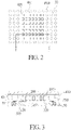
- FIG. 2 is a perspective top view showing an exemplary layout of the dummy metal features on the interposer, wherein like numeral numbers designate like elements, regions or layers.
- FIG. 3 is a cross-sectional view taken along line I-I' in FIG. 2 . As shown in FIG. 2 and FIG. 3 , a 7x7 copper pillar or bump array is demonstrated as an example of the dummy metal features on the interposer. It is to be understood that the layout and number of the dummy metal features 420 and the peripheral solder balls PSB are for illustration purposes only. In FIG. 3 , the dummy metal features 420 are not in direct contact with the bottom surface 200b of the package substrate 200.
- the heat dissipation efficiency may be further improved.
- the capillary underfill 410, the dummy metal features 420 or the dummy pads 320 may function as a heat dissipating element of the POP1.
- the dummy metal features 420 may be in direct contact with the bottom surface 200b of the package substrate 200.
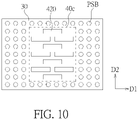
- FIG. 4 to FIG. 10 illustrate various layout of the dummy metal features on the interposer according to some embodiments, wherein FIG. 7 is a cross-sectional view taken along line II-II' in FIG. 6 and FIG. 9 is a cross-sectional view taken along line III-III' in FIG. 8 .
- the dummy metal features 420 may be aligned with one another along a first direction D1 and are arranged in a staggered manner along a second direction D2.
- the dummy metal features 420 may be arranged within a circular region 40c'.
- the dummy metal features 420 may be solder balls. In FIG. 7 , the dummy metal features 420 are not in direct contact with the bottom surface 200b of the package substrate 200. However, it is understood that in some embodiments, the dummy metal features 420 may be in direct contact with the bottom surface 200b of the package substrate 200.
- the dummy metal features 420 may have a cylindrical shape. In FIG. 9 , the dummy metal features 420 are not in direct contact with the bottom surface 200b of the package substrate 200. However, it is understood that in some embodiments, the dummy metal features 420 may be in direct contact with the bottom surface 200b of the package substrate 200.
- each of the dummy metal features 420 may have a strip shape or a bar shape extending along the first direction D1 and arranged in a staggered manner along the second direction D2.
- the capillary underfill 410 may be injected into the gap 40 along the first direction D1.
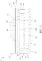
- FIG. 11 is a schematic, cross-sectional diagram showing an exemplary PoP according to another embodiment of the invention.
- the PoP 2 comprises a bottom package 10 and a top package 20 stacked on the bottom package 10.
- the top package 20 may be a memory package, but not limited thereto.
- the bottom package 10 may comprise a semiconductor chip 101 mounted on a package substrate 100 in a flip-chip manner.
- the package substrate 100 may comprise a three-layer or four-layer coreless embedded trace substrate (ETS), but not limited thereto.
- the semiconductor chip 101 such as a logic die or a system on a chip may be electrically connected to the package substrate 100 through a plurality of connecting elements 112 such as copper bumps, pillars or micro-bumps, but not limited thereto.
- a plurality of BGA balls SB may be provided on a lower surface of the package substrate 100.
- the pitch of the BGA balls SB at the lower surface of the package substrate 100 may be equal to or smaller than 0.35 mm, but not limited thereto.
- the semiconductor chip 101 may be encapsulated by an over-mold 140, for example, an engineering molding compound.
- the top package 20 may comprise at least one memory chip 201 mounted on a package substrate 200.
- the memory chip 201 may be a HBM or a LPDRAM chip, but not limited thereto.
- the memory chip 201 may be electrically connected to the package substrate 200 through bond wires 203.
- the memory chip 201, the bond wires 203, and the top surface 200a of the package substrate 200 are encapsulated by an over-mold 240.
- the top package 20 is electrically connected to the bottom package 10 through an intervening interposer 30.
- the interposer 30 may be a two-layer cored substrate, but not limited thereto.
- the interposer 30 may comprise interconnect structure 301 that is electrically connected to through mold vias 150 such as copper pillars that are embedded in the over-mold 140 and disposed around the perimeter of the semiconductor chip 101.
- the top package 20 is mounted on the interposer 30 and is electrically connected to the interposer 30 through the plurality of peripheral solder balls PSB.
- a small gap 40 is formed between the top package 20 and the interposer 30.
- a thermal die 50 such as a dummy silicon die is provided on the interposer 30 and is surrounded by the peripheral solder balls PSB.
- the thermal die 50 may be adhered to a top surface of the interposer 30 by using an adhesive layer 510.
- the thermal die 50 has a height that is smaller than that of the peripheral solder balls PSB, so that the thermal die 50 is not in direct contact with the bottom surface 200b of the package substrate 200.
- the thermal die 50 may be electrically floating, meaning that no connection is formed under the thermal die 50 to electrically connect the thermal die 50 to any other interconnect structure in the interposer 30. It is also beneficial to use the thermal die 50 to dissipate the heat generated by the semiconductor chip 101 because using the thermal die 50 is more cost-effective.
Landscapes
- Wire Bonding (AREA)
- Structures Or Materials For Encapsulating Or Coating Semiconductor Devices Or Solid State Devices (AREA)
- Cooling Or The Like Of Semiconductors Or Solid State Devices (AREA)
Applications Claiming Priority (3)
| Application Number | Priority Date | Filing Date | Title |
|---|---|---|---|
| US202063128899P | 2020-12-22 | 2020-12-22 | |
| US202163137774P | 2021-01-15 | 2021-01-15 | |
| US17/492,693 US12021068B2 (en) | 2020-12-22 | 2021-10-04 | Semiconductor device with dummy thermal features on interposer |
Publications (1)
| Publication Number | Publication Date |
|---|---|
| EP4020554A1 true EP4020554A1 (de) | 2022-06-29 |
Family
ID=78528656
Family Applications (1)
| Application Number | Title | Priority Date | Filing Date |
|---|---|---|---|
| EP21203716.2A Pending EP4020554A1 (de) | 2020-12-22 | 2021-10-20 | Halbleiterbauelement mit thermischen dummy-eigenschaften auf einem interposer |
Country Status (4)
| Country | Link |
|---|---|
| US (1) | US12021068B2 (de) |
| EP (1) | EP4020554A1 (de) |
| CN (1) | CN114664761A (de) |
| TW (1) | TWI795059B (de) |
Families Citing this family (8)
| Publication number | Priority date | Publication date | Assignee | Title |
|---|---|---|---|---|
| EP4325561A4 (de) | 2022-07-08 | 2024-12-11 | Changxin Memory Technologies, Inc. | Halbleiterverpackungsstruktur und herstellungsverfahren |
| CN117410242A (zh) | 2022-07-08 | 2024-01-16 | 长鑫存储技术有限公司 | 半导体封装组件及制备方法 |
| CN117410261A (zh) * | 2022-07-08 | 2024-01-16 | 长鑫存储技术有限公司 | 半导体封装结构及制备方法 |
| US20240038614A1 (en) * | 2022-08-01 | 2024-02-01 | Mediatek Inc. | Semiconductor package structure |
| US12347739B2 (en) * | 2022-08-26 | 2025-07-01 | Taiwan Semiconductor Manufacturing Company, Ltd. | Package structure |
| CN115662959B (zh) * | 2022-12-26 | 2023-09-26 | 长电集成电路(绍兴)有限公司 | 一种芯片封装结构及其制备方法 |
| US20240332251A1 (en) * | 2023-04-02 | 2024-10-03 | Intel Corporation | Dummy silicon stiffening mechanism for module warpage mitigation |
| US20250210608A1 (en) | 2023-12-26 | 2025-06-26 | Taiwan Semiconductor Manufacturing Co., Ltd. | Integrated circuit packages with thermal reservoir dies and methods of forming the same |
Citations (5)
| Publication number | Priority date | Publication date | Assignee | Title |
|---|---|---|---|---|
| US20080308950A1 (en) * | 2007-06-12 | 2008-12-18 | Samsung Electro-Mechanics Co., Ltd. | Semiconductor package and method for manufacturing thereof |
| US20180269188A1 (en) * | 2017-03-15 | 2018-09-20 | Taiwan Semiconductor Manufacturing Company, Ltd. | Semiconductor packages and methods of forming same |
| US20190115326A1 (en) * | 2016-09-14 | 2019-04-18 | Taiwan Semiconductor Manufacturing Company, Ltd. | Semiconductor Packages having Dummy Connectors and Methods of Forming Same |
| US20190311996A1 (en) * | 2017-01-05 | 2019-10-10 | Huawei Technologies Co., Ltd. | High-Reliability Electronic Packaging Structure, Circuit Board, and Device |
| US20190333900A1 (en) * | 2014-03-07 | 2019-10-31 | Taiwan Semiconductor Manufacturing Company, Ltd. | Solution for Reducing Poor Contact in InFO Package |
Family Cites Families (5)
| Publication number | Priority date | Publication date | Assignee | Title |
|---|---|---|---|---|
| KR100702969B1 (ko) * | 2005-04-19 | 2007-04-03 | 삼성전자주식회사 | 더미 솔더 볼을 갖는 bga형 반도체 칩 패키지의 기판 실장 구조 |
| US10079192B2 (en) | 2015-05-05 | 2018-09-18 | Mediatek Inc. | Semiconductor chip package assembly with improved heat dissipation performance |
| US9437536B1 (en) * | 2015-05-08 | 2016-09-06 | Invensas Corporation | Reversed build-up substrate for 2.5D |
| KR102544776B1 (ko) * | 2016-04-28 | 2023-06-20 | 삼성전자주식회사 | 반도체 패키지의 제조 방법 |
| US10566261B2 (en) | 2017-11-15 | 2020-02-18 | Taiwan Semiconductor Manufacturing Company, Ltd. | Integrated fan-out packages with embedded heat dissipation structure |
-
2021
- 2021-10-04 US US17/492,693 patent/US12021068B2/en active Active
- 2021-10-20 EP EP21203716.2A patent/EP4020554A1/de active Pending
- 2021-10-28 CN CN202111265545.1A patent/CN114664761A/zh active Pending
- 2021-11-03 TW TW110140931A patent/TWI795059B/zh active
Patent Citations (5)
| Publication number | Priority date | Publication date | Assignee | Title |
|---|---|---|---|---|
| US20080308950A1 (en) * | 2007-06-12 | 2008-12-18 | Samsung Electro-Mechanics Co., Ltd. | Semiconductor package and method for manufacturing thereof |
| US20190333900A1 (en) * | 2014-03-07 | 2019-10-31 | Taiwan Semiconductor Manufacturing Company, Ltd. | Solution for Reducing Poor Contact in InFO Package |
| US20190115326A1 (en) * | 2016-09-14 | 2019-04-18 | Taiwan Semiconductor Manufacturing Company, Ltd. | Semiconductor Packages having Dummy Connectors and Methods of Forming Same |
| US20190311996A1 (en) * | 2017-01-05 | 2019-10-10 | Huawei Technologies Co., Ltd. | High-Reliability Electronic Packaging Structure, Circuit Board, and Device |
| US20180269188A1 (en) * | 2017-03-15 | 2018-09-20 | Taiwan Semiconductor Manufacturing Company, Ltd. | Semiconductor packages and methods of forming same |
Also Published As
| Publication number | Publication date |
|---|---|
| TWI795059B (zh) | 2023-03-01 |
| US20220199593A1 (en) | 2022-06-23 |
| US12021068B2 (en) | 2024-06-25 |
| CN114664761A (zh) | 2022-06-24 |
| TW202226503A (zh) | 2022-07-01 |
Similar Documents
| Publication | Publication Date | Title |
|---|---|---|
| US12021068B2 (en) | Semiconductor device with dummy thermal features on interposer | |
| US10410968B2 (en) | Semiconductor package and method of manufacturing the same | |
| EP2775512B1 (de) | Halbleiterbauelemente | |
| US8338929B2 (en) | Stacked-type chip package structure and fabrication method thereof | |
| US9502335B2 (en) | Package structure and method for fabricating the same | |
| US20250343191A1 (en) | Semiconductor Package | |
| TWI685071B (zh) | 半導體封裝結構 | |
| US12469790B2 (en) | Semiconductor package and method of manufacturing the same | |
| EP3035383A1 (de) | Halbleitergehäuseanordnung | |
| TWI818458B (zh) | 電子封裝件及其製法 | |
| CN115295540A (zh) | 半导体封装 | |
| EP4135032A1 (de) | Halbleitergehäuse mit reduzierter verbindungslänge | |
| US20250174576A1 (en) | Semiconductor package and fabrication method thereof | |
| US20130256915A1 (en) | Packaging substrate, semiconductor package and fabrication method thereof | |
| EP4404246A1 (de) | Halbleitergehäuse und herstellungsverfahren dafür | |
| US20240071951A1 (en) | Semiconductor package and method of fabricating the same | |
| US9136219B2 (en) | Expanded semiconductor chip and semiconductor device | |
| CN116264190A (zh) | 半导体封装件 | |
| TWI732583B (zh) | 半導體封裝件 | |
| US20250062279A1 (en) | Semiconductor package and method of fabricating the same | |
| US20240153886A1 (en) | Semiconductor package | |
| US20200118972A1 (en) | Semiconductor package | |
| CN118352323A (zh) | 半导体封装 | |
| KR101185858B1 (ko) | 반도체 칩 및 이를 갖는 적층 반도체 패키지 | |
| US20250246585A1 (en) | Semiconductor package |
Legal Events
| Date | Code | Title | Description |
|---|---|---|---|
| PUAI | Public reference made under article 153(3) epc to a published international application that has entered the european phase |
Free format text: ORIGINAL CODE: 0009012 |
|
| STAA | Information on the status of an ep patent application or granted ep patent |
Free format text: STATUS: THE APPLICATION HAS BEEN PUBLISHED |
|
| AK | Designated contracting states |
Kind code of ref document: A1 Designated state(s): AL AT BE BG CH CY CZ DE DK EE ES FI FR GB GR HR HU IE IS IT LI LT LU LV MC MK MT NL NO PL PT RO RS SE SI SK SM TR |
|
| STAA | Information on the status of an ep patent application or granted ep patent |
Free format text: STATUS: REQUEST FOR EXAMINATION WAS MADE |
|
| 17P | Request for examination filed |
Effective date: 20221229 |
|
| RBV | Designated contracting states (corrected) |
Designated state(s): AL AT BE BG CH CY CZ DE DK EE ES FI FR GB GR HR HU IE IS IT LI LT LU LV MC MK MT NL NO PL PT RO RS SE SI SK SM TR |
|
| P01 | Opt-out of the competence of the unified patent court (upc) registered |
Effective date: 20230607 |