EP4018230B1 - Herstellung von oberflächenreliefstrukturen - Google Patents
Herstellung von oberflächenreliefstrukturen Download PDFInfo
- Publication number
- EP4018230B1 EP4018230B1 EP20761879.4A EP20761879A EP4018230B1 EP 4018230 B1 EP4018230 B1 EP 4018230B1 EP 20761879 A EP20761879 A EP 20761879A EP 4018230 B1 EP4018230 B1 EP 4018230B1
- Authority
- EP
- European Patent Office
- Prior art keywords
- substrate
- etchant
- etching
- etched
- surface relief
- Prior art date
- Legal status (The legal status is an assumption and is not a legal conclusion. Google has not performed a legal analysis and makes no representation as to the accuracy of the status listed.)
- Active
Links
Images




Classifications
-
- B—PERFORMING OPERATIONS; TRANSPORTING
- B05—SPRAYING OR ATOMISING IN GENERAL; APPLYING FLUENT MATERIALS TO SURFACES, IN GENERAL
- B05C—APPARATUS FOR APPLYING FLUENT MATERIALS TO SURFACES, IN GENERAL
- B05C3/00—Apparatus in which the work is brought into contact with a bulk quantity of liquid or other fluent material
- B05C3/02—Apparatus in which the work is brought into contact with a bulk quantity of liquid or other fluent material the work being immersed in the liquid or other fluent material
-
- B—PERFORMING OPERATIONS; TRANSPORTING
- B05—SPRAYING OR ATOMISING IN GENERAL; APPLYING FLUENT MATERIALS TO SURFACES, IN GENERAL
- B05D—PROCESSES FOR APPLYING FLUENT MATERIALS TO SURFACES, IN GENERAL
- B05D1/00—Processes for applying liquids or other fluent materials
- B05D1/18—Processes for applying liquids or other fluent materials performed by dipping
-
- B—PERFORMING OPERATIONS; TRANSPORTING
- B81—MICROSTRUCTURAL TECHNOLOGY
- B81C—PROCESSES OR APPARATUS SPECIALLY ADAPTED FOR THE MANUFACTURE OR TREATMENT OF MICROSTRUCTURAL DEVICES OR SYSTEMS
- B81C1/00—Manufacture or treatment of devices or systems in or on a substrate
- B81C1/00436—Shaping materials, i.e. techniques for structuring the substrate or the layers on the substrate
- B81C1/00523—Etching material
-
- B—PERFORMING OPERATIONS; TRANSPORTING
- B81—MICROSTRUCTURAL TECHNOLOGY
- B81C—PROCESSES OR APPARATUS SPECIALLY ADAPTED FOR THE MANUFACTURE OR TREATMENT OF MICROSTRUCTURAL DEVICES OR SYSTEMS
- B81C1/00—Manufacture or treatment of devices or systems in or on a substrate
- B81C1/00436—Shaping materials, i.e. techniques for structuring the substrate or the layers on the substrate
- B81C1/00523—Etching material
- B81C1/00539—Wet etching
-
- B—PERFORMING OPERATIONS; TRANSPORTING
- B81—MICROSTRUCTURAL TECHNOLOGY
- B81C—PROCESSES OR APPARATUS SPECIALLY ADAPTED FOR THE MANUFACTURE OR TREATMENT OF MICROSTRUCTURAL DEVICES OR SYSTEMS
- B81C1/00—Manufacture or treatment of devices or systems in or on a substrate
- B81C1/00436—Shaping materials, i.e. techniques for structuring the substrate or the layers on the substrate
- B81C1/00555—Achieving a desired geometry, i.e. controlling etch rates, anisotropy or selectivity
-
- B—PERFORMING OPERATIONS; TRANSPORTING
- B81—MICROSTRUCTURAL TECHNOLOGY
- B81C—PROCESSES OR APPARATUS SPECIALLY ADAPTED FOR THE MANUFACTURE OR TREATMENT OF MICROSTRUCTURAL DEVICES OR SYSTEMS
- B81C1/00—Manufacture or treatment of devices or systems in or on a substrate
- B81C1/00436—Shaping materials, i.e. techniques for structuring the substrate or the layers on the substrate
- B81C1/00555—Achieving a desired geometry, i.e. controlling etch rates, anisotropy or selectivity
- B81C1/00626—Processes for achieving a desired geometry not provided for in groups B81C1/00563 - B81C1/00619
-
- B—PERFORMING OPERATIONS; TRANSPORTING
- B81—MICROSTRUCTURAL TECHNOLOGY
- B81C—PROCESSES OR APPARATUS SPECIALLY ADAPTED FOR THE MANUFACTURE OR TREATMENT OF MICROSTRUCTURAL DEVICES OR SYSTEMS
- B81C1/00—Manufacture or treatment of devices or systems in or on a substrate
- B81C1/00436—Shaping materials, i.e. techniques for structuring the substrate or the layers on the substrate
- B81C1/00634—Processes for shaping materials not provided for in groups B81C1/00444 - B81C1/00626
-
- G—PHYSICS
- G02—OPTICS
- G02B—OPTICAL ELEMENTS, SYSTEMS OR APPARATUS
- G02B5/00—Optical elements other than lenses
- G02B5/18—Diffraction gratings
- G02B5/1847—Manufacturing methods
- G02B5/1857—Manufacturing methods using exposure or etching means, e.g. holography, photolithography, exposure to electron or ion beams
-
- G—PHYSICS
- G02—OPTICS
- G02B—OPTICAL ELEMENTS, SYSTEMS OR APPARATUS
- G02B6/00—Light guides; Structural details of arrangements comprising light guides and other optical elements, e.g. couplings
- G02B6/10—Light guides; Structural details of arrangements comprising light guides and other optical elements, e.g. couplings of the optical waveguide type
- G02B6/12—Light guides; Structural details of arrangements comprising light guides and other optical elements, e.g. couplings of the optical waveguide type of the integrated circuit kind
- G02B6/13—Integrated optical circuits characterised by the manufacturing method
- G02B6/136—Integrated optical circuits characterised by the manufacturing method by etching
-
- G—PHYSICS
- G03—PHOTOGRAPHY; CINEMATOGRAPHY; ANALOGOUS TECHNIQUES USING WAVES OTHER THAN OPTICAL WAVES; ELECTROGRAPHY; HOLOGRAPHY
- G03F—PHOTOMECHANICAL PRODUCTION OF TEXTURED OR PATTERNED SURFACES, e.g. FOR PRINTING, FOR PROCESSING OF SEMICONDUCTOR DEVICES; MATERIALS THEREFOR; ORIGINALS THEREFOR; APPARATUS SPECIALLY ADAPTED THEREFOR
- G03F7/00—Photomechanical, e.g. photolithographic, production of textured or patterned surfaces, e.g. printing surfaces; Materials therefor, e.g. comprising photoresists; Apparatus specially adapted therefor
- G03F7/0005—Production of optical devices or components in so far as characterised by the lithographic processes or materials used therefor
-
- G—PHYSICS
- G03—PHOTOGRAPHY; CINEMATOGRAPHY; ANALOGOUS TECHNIQUES USING WAVES OTHER THAN OPTICAL WAVES; ELECTROGRAPHY; HOLOGRAPHY
- G03F—PHOTOMECHANICAL PRODUCTION OF TEXTURED OR PATTERNED SURFACES, e.g. FOR PRINTING, FOR PROCESSING OF SEMICONDUCTOR DEVICES; MATERIALS THEREFOR; ORIGINALS THEREFOR; APPARATUS SPECIALLY ADAPTED THEREFOR
- G03F7/00—Photomechanical, e.g. photolithographic, production of textured or patterned surfaces, e.g. printing surfaces; Materials therefor, e.g. comprising photoresists; Apparatus specially adapted therefor
- G03F7/0005—Production of optical devices or components in so far as characterised by the lithographic processes or materials used therefor
- G03F7/001—Phase modulating patterns, e.g. refractive index patterns
Definitions
- Optical gratings are components having a repeating pattern of lines with which light propagating in the component, or impingent on it, interacts.
- the grating causes diffraction of the light such that its direction of propagation may be altered.
- Gratings may operate in a transmissive or reflective mode.
- lines of a grating are formed by physical features on the surface of a component, for example by etching the surface of the material, and hence optical gratings formed in this way are examples of surface relief structures.
- a grating within a component may be formed by creating a grating (i.e. a surface relief structure) on the surface of a first part and joining that part to a second part so that the grating is within the resulting component.
- HUDs Head Up, or Head Mounted Displays
- HMDs Head Mounted Displays
- other head-worn displays which overlay an image on the user's view of the real world. This is achieved by providing a transparent component in the user's line of sight which projects the required image to the user's eyes.
- the transparent component may be on a helmet or may otherwise be head-worn (e.g. in a HMD) or the transparent component may be mounted in the vehicle (e.g. aeroplane or land vehicle) in which the user sits (e.g. in a HUD).
- Optical gratings may be utilised to couple light into, and out of, the transparent component.
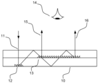
- Figure 1 shows schematic cross-section of a typical configuration of an optical waveguide 10 for a HUD. The configuration within a HMD may be similar to that shown in Figure 1 .
- Image light is injected at point 11, and diffracted by optical grating 12 such that the light travels at angle that will be guided by total internal reflection in the waveguide 10.
- the light is then coupled out of the waveguide by optical grating 13 to a user's eye 14.
- the light should be coupled out of the waveguide over an area of an exit pupil as represented by rays 15, 16 at the edges of that pupil.
- the image intensity across the exit pupil should be constant such that any movement between the eye and waveguide does not cause a change in intensity.
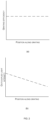
- an output grating 13 with constant efficiency does not provide such even Intensity.
- a constant-efficiency grating couples same portion of light out of the grating at all points. Hence the actual light intensity coupled out decreases along the length of the grating as shown in Figure 2b .
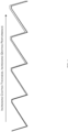
- This variation can be avoided by utilising a variable efficiency grating whereby the portion of light coupled out varies along the grating as shown in Figure 3a .
- the variation in grating efficiency provides a constant output intensity as shown in Figure 3b .
- a method and apparatus for the etching of variable depth features in a substrate is described. Movement of the substrate relative to an etchant (e.g. into or out of the etchant) during the etching process is utilised to provide a varying etch time, and hence depth, across the substrate, and in various examples this is enabled without requiring a varying mask.
- an etchant e.g. into or out of the etchant
- a first aspect provides a method of etching a surface relief structure in a substrate, the method comprising the steps of: moving the substrate between a first position and a second position in an etching system; wherein in the first position only a first part of the area to be etched is exposed to an etchant, and in the second position the whole area to be etched is exposed to the etchant such that the first part of the area to be etched is exposed to the etchant for a longer period of time than at least one other part of the whole area to be etched; and wherein the movement is defined according to the etching profile required, and removing the substrate from the etching fluid when etching is complete.
- the surface relief structure comprises a blazed surface relief structure.
- the etchant comprises an anisotropic etchant.
- Moving the substrate between the first position and the second position in the etching system may comprise either moving the substrate from the first position to the second position or moving the substrate from the second position to the first position.
- the surface relief structure comprises a variable depth etching profile.
- both the movement of the substrate and an orientation of the substrate relative to the etchant surface may be defined according to the etching profile required
- the method may further comprise, prior to moving the substrate between the first position and the second position: preparing a substrate to be etched with an etch-resist mask.
- the method may additionally, further comprise, after removing the substrate from the etchant: removing any remaining etch-resist mask from the substrate.
- the movement between the first position and the second position may be along an axis substantially perpendicular to a surface of the etchant.
- the etch profile may be a non-linear profile.
- the movement between the first position and the second position may comprise a series of discrete steps.
- step may be the same size.
- the steps are of varying sizes.
- the time between each step may be constant or the time between each step may be variable.
- the movement between the first position and the second position may comprise a continuous movement.
- the continuous movement may be at a constant speed. In other examples, the continuous movement may be at a variable speed.
- the surface relief structure may be an optical grating.
- the axis of movement may be aligned with the axis of the grating.
- the surface relief structure may be an array of facets.
- the resulting structure with the surface relief structure may be an optical master.
- the substrate is a substrate formed of a crystalline material.
- the substrate may be a silicon wafer.
- the substrate is an off-axis silicon wafer.
- the substrate may be suspended by a suspension apparatus into an etching vessel.
- the substrate may be moved between the first position and the second position by the suspension apparatus lowering the substrate into the etching vessel of the etching system.
- Moving the substrate between the first position and the second position in the etching system may be the first time the substrate is etched, such that the substrate is un-etched immediately prior to moving the substrate between a first position and a second position in the etching system.
- a second aspect provides an etching system for etching a surface relief structure in a substrate comprising: an etching vessel; and a support apparatus arranged to move the substrate between a first position and a second position in the etching system; wherein in the first position only a first part of the area to be etched is exposed to an etchant in the etching vessel, and in the second position the whole area to be etched is exposed to the etchant such that the first part of the area to be etched is exposed to the etchant for a longer period of time than at least one other part of the whole area to be etched; and wherein the movement is defined according to the etching profile required.
- the surface relief structure comprises a blazed surface relief structure.
- the etchant comprises an anisotropic etchant.
- the support apparatus may comprise a suspension apparatus arranged to move the substrate between the first position and the second position in the etching system by lowering the substrate into the etching vessel or by raising the substrate out of the etching vessel.
- the following disclosure sets out a new method for producing surface relief structures on a substrate.
- the structure may be a nanostructure or alternatively the features may be on a larger scale (e.g. features that are tens or hundreds of microns wide and/or deep).
- the surface relief structures may comprise an array of facets which may, for example, form an optical component that may be used for diffraction (e.g. optical gratings, such as a graded optical grating), reflection (e.g. mirror arrays) or refraction (e.g. prismatic arrays) or any combination thereof.
- the surface relief structure may form an optical master which is then replicated (e.g. by moulding) to form a plurality of identical optical elements (e.g. copies of the optical master).
- the optical components formed using the surface relief structures (or comprising the surface relief structures) may be used in HUDs, HMDs or other head-worn displays (e.g. to provide a more uniform intensity across a display).
- the facets may be blazed.
- the substrate in which the surface relief structure is formed by means of a wet etch is formed from a crystalline material, such as silicon, or, in examples not according to the claimed invention, is formed from a non-crystalline material, such as glass or metal.
- the substrate is formed from a crystalline material (e.g. silicon)
- the etching preferentially etches along some crystal planes.
- the substrate may be an off-axis silicon wafer (or part thereof), such as a wafer with a ⁇ 100> orientation top plane where the etching exposes the ⁇ 111 ⁇ planes within the silicon. These exposed planes may form the facets of an array of facets or grating lines within the surface relief structure.
- a silicon wafer is an example of a semiconductor wafer and in various examples, the substrate may be another type of semiconductor wafer.
- the etchant (or etching liquid) used may be any suitable liquid.
- the substrate may be a semiconductor wafer, for example silicon, and the etchant may be any liquid known for etching such wafers (e.g. acids such as hydrofluoric acid, HF, or buffered HF, nitric acid, or strongly alkaline solutions).
- the method comprises gradually inserting the substrate into or removing the substrate from the etchant, such that different parts of the substrate are etched for different amounts of time. This results in a controlled variation in etch depth across the resulting surface relief structure, which is proportional to the time spent within the etchant.
- any reference to 'a part' of a substrate or area to be etched refers to a part that is smaller than the entirety of the substrate or area to be etched respectively.
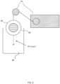
- Figure 5 shows a schematic diagram of an example apparatus which may be utilised to implement the method described hereinbelow.
- An etching vessel 50 (e.g. an etch tank) is provided for containing a liquid for etching a substrate.
- the vessel may be a conventional etch tank as known in the art and be used to contain conventional or proprietary etching liquids.
- Other apparatus typically associated with an etching system is also present as required, but is not shown for clarity.
- a suspension apparatus 51 is provided to suspend a substrate 52 for etching within the vessel 50.
- the suspension apparatus 51 enables the height of the substrate within the vessel to be varied.
- a winch system is provided utilising a wire to suspend the substrate.
- the wire is attached to the substrate at its distal end, and at its proximal end to a control system for extending and retracting the wire.
- a pulley arrangement may be utilised to guide the wire and support the substrate in the required location.
- the substrate 52 may not be suspended but may be otherwise supported or held in place and moved into and out of the etchant (in the etching vessel 50) and in such examples, the suspension apparatus 51 may be replaced by an alternative substrate support or mounting apparatus.
- the suspension, or mounting apparatus enables the gradual movement of the substrate along an axis, which may be in the plane of the substrate, into and out of the etchant.
- the substrate has a etch resist mask 53 (e.g. in the form of an oxide layer) deposited on one or more surfaces such that areas to be etched are exposed to the etchant upon placement in the vessel, and areas not to be etched are protected from the etchant by the mask, as is known in the art.
- a etch resist mask 53 e.g. in the form of an oxide layer
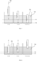
- Figure 6 shows a flow chart of a method of etching using the apparatus of Figure 5 and this can be described with reference to the two examples shown in Figures 7 and 8 and with reference to Figure 10 .
- an etch-resist mask is applied to the substrate to be etched (block 602, Figure 10a ) and this may be applied in the conventional manner.
- This application of the etch-resist mask may be part of the method or alternatively, precoated substrates (i.e. with the etch-resist mask already applied) may be received.
- a constant linewidth mask is utilised as is known in the art for producing constant efficiency gratings. Since this mask is regular no special techniques are required for its production.
- a different mask may be used to create other surface relief features and in various examples the mask may not have constant linewidth and/or constant pitch.
- the mask may define openings (i.e. areas for etching) that are all rectangular and in other examples, the openings may be of different (or varying) shape.
- the substrate is mounted in or above the etching vessel 50 (e.g. suspended by the suspension apparatus 51 in or above the etching vessel 50), but not within the etchant.
- the substrate is mounted above the surface 702 of the etchant 704.
- the substrate is mounted (e.g. suspended) such that the areas which require more etching are positioned closest to the etchant.
- the mask layout and suspension arrangement may be such that the end of an optical grating to be formed with higher efficiency are closest to the etchant.
- the substrate is then moved (e.g. lowered) to a first position, P1, in the etchant (block 606) and etching of the areas of the substrate exposed to the etchant commences.
- t the first position only part of the overall area to be etched (i.e. not the entirety of the overall area to be etched) may be exposed to the etchant (e.g. as in Figure 7 ) or all of the area to be etched may be exposed to the etchant (e.g. as in Figure 8 ).
- the position of the substrate in the etchant is changed, e.g. to a second position, P2, in the etchant (block 608).
- This comprises moving the substrate into or out of the etchant by a predefined amount, such that a different proportion (or portion) of the substrate is exposed to the etchant.
- the example in Figure 7 shows the substrate being moved further into the etchant (i.e. such that more of the substrate is exposed to the etchant) and the example in Figure 8 shows the substrate being moved further out of the etchant (i.e. such that less of the substrate is exposed to the etchant).
- the motion of the substrate will be along a defined axis 706 that is in the plane of the substrate and substantially perpendicular to the surface of the etchant 702 (e.g. the axis is defined by the suspension apparatus 51 in Figure 5 ) such that the motion of the substrate (in block 608) is into or out of the etchant, instead of laterally within the etchant.
- the repositioning of the substrate in the etchant may be repeated multiple times (as indicated by the arrow from block 608 back to block 608 in Figure 6 ). For example, the substrate may be incrementally lowered into the etchant until the whole area to be etched is exposed or incrementally raised out of the etchant until none of the substrate is exposed to the etchant.
- the substrate is removed from the etchant (block 610) and processed in the normal manner (e.g. including removal of the etch-resist mask, block 612).
- Figure 10b shows an example substrate following removal from the etchant (in block 610) and Figure 10c shows the same example substrate following removal of the etch-resist mask (in block 612).
- the result of the process of Figure 6 is that different areas of the substrate (or of the area to be etched) are exposed to the etchant for different amounts of time and are therefore etched by different amounts, i.e. there is a variation in etch depth across the substrate, as shown in the examples in Figure 9 (described below).
- the surface relief structure being formed is an optical grating
- the axis of optical grating may be aligned with the axis of movement of the substrate into the etching fluid 706 and hence a graded depth of grating features is achieved along the grating and hence a graded efficiency. This is achieved without the need for non-conventional masks or specific processing techniques.
- a graded efficiency grating can thus be provided without significant additional complexity.
- the etch depth variation across the substrate can be accurately controlled.
- a linear depth profile may be obtained and in other examples a non-linear (e.g. polynomial) depth profile may be obtained.
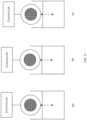
- the depth profile across the area to be etched may also be controlled by controlling the angle at which the substrate is moved into and/or out of the etchant with respect to the features on the etch-resist mask and three examples are shown in Figure 11 .
- This control of the angle may be achieved by mounting the substrate with the appropriate orientation into the apparatus (in block 604).
- Figure 11a shows an example arrangement in which the movement into / out of the etchant is orthogonal to the lines in the etch-resist mask that form the etched facets.
- Figure 11b shows an example arrangement shows an example arrangement in which the movement into / out of the etchant is angularly offset to the lines in the etch-resist mask that form the etched facets.
- Figure 11c shows an example arrangement shows an example arrangement in which the movement into / out of the etchant is parallel to the lines in the etch-resist mask that form the etched facets.
- the substrate may then be remounted on the apparatus in a different orientation (in block 604) and the method repeated (e.g. as indicated by the dotted arrow from block 610 to block 604 in Figure 6 ).
- both (or all) passes of the method of Figure 6 use the same etch-resist mask and hence result in the etching of the same areas of the substrate.
- the method may involve removing the first etch-resist mask (in block 612) and applying a second, different etch-resist mask (in block 602) before repeating the etch process described above (e.g. as indicated by the dotted arrow from block 612 to block 602 in Figure 6 ).
- the properties of the etchant 704 are substantially constant throughout the body of the etchant.
- the properties of the etchant may vary within the etching vessel 50, e.g. there may be a temperature gradient within the etching vessel 50 that results in the etching characteristics of the etchant (e.g. the etch rate) varying within the etching vessel 50.
- the etchant may be differentially agitated within the etching vessel 50 such that the etching characteristics of the etchant (e.g. the etch rate) vary within the etching vessel 50.
- the resulting surface relief structure on the substrate (which may, for example, be a silicon master grating) may then be replicated and, where needed, coated (with a uniform thickness) to provide multiple optical components (e.g. multiple gratings) for use.
- the movement of the substrate may comprise a series of discrete steps, with the size of the steps and/or the time between them defined as required to etch the desired profile.
- constant step and/or time gaps may be utilised, or variable step and/or time gaps may be utilised.
- the movement may be continuous, rather than discrete steps, and can progress at any constant or variable speed. Controlling the rate of movement of the substrate thus allows any desired etch depth profile to be created, thus allowing the creation of optimum efficiency profiles as required for applications. Even complex profiles may, in various examples, still utilise a conventional linear mask.
- the movement of the substrate into the etchant thus defines the etching profile required.
- Figure 9 shows schematic diagrams of three example etched substrates where the substrate is formed from a crystalline material such as silicon and the etch preferentially etches some planes within the crystal.
- the first example shown in Figure 9a , shows binary grooves (e.g. which may be formed in non-crystalline substrates).
- the second example, shown in Figure 9b shows v-shaped grooves, although as shown in Figure 9b , dependent upon the line width of the openings in the etch-resist mask and the etch times used, some of the etched features may etch to termination (e.g. as shown by the v-shaped groove 902) and other features may not etch to termination (e.g. as shown by the more u-shaped features 904).
- the third example, shown in Figure 9c shows blazed grooves, which may, for example, be achieved through use of an appropriate off-axis crystalline substrate.
- Use of such blazed grooves may further enable the tailoring of the surface relief structure to improve diffraction efficiency (e.g. where the surface relief structure formed is a blazed optical grating).
- the shape of the etched regions will be dependent on the substrate material and the choice of etchant as well as the etch depth. In all examples, there is a variation in the etch depth of the etched features across the substrate (e.g. d 1 ⁇ d 2 ⁇ d 3 ).
- the use of an anisotropic etchant may improve the formation of the blazed structure allowing such a structure to be formed from a blank or un-etched substrate.
- An un-etched substrate may refer to a substrate that has a substantially flat surface.
- An un-etched or blank substrate may be cleaned prior to etching, for example to remove contaminants or oxide layers.
- the surface relief structures formed by the methods described herein may form many different types of optical elements, including optical gratings, optical facets and optical mirror arrays, etc.
- the resultant structure may not itself be used as an optical element but may be used as a master to form (e.g. via moulding) a plurality of copies that are then used as optical elements.
- the optical elements may themselves then form part of a HUD, HMD or other head-worn device.
- the method described above may, for example, be used to generate a variable efficiency optical grating that may be used to improve the uniformity of intensity output over the length of the grating.
- the variation in etch depth results in a variation in sampling of incident light (e.g. as a consequence of the differing lengths of the mirror facets).
Landscapes
- Physics & Mathematics (AREA)
- Engineering & Computer Science (AREA)
- Manufacturing & Machinery (AREA)
- General Physics & Mathematics (AREA)
- Microelectronics & Electronic Packaging (AREA)
- Optics & Photonics (AREA)
- Geometry (AREA)
- Diffracting Gratings Or Hologram Optical Elements (AREA)
- ing And Chemical Polishing (AREA)
- Manufacture Or Reproduction Of Printing Formes (AREA)
Claims (15)
- Verfahren zum Ätzen einer geflammten Oberflächenreliefstruktur in einem Substrat, wobei das Verfahren die folgenden Schritte umfasst:Bewegen des Substrats zwischen einer ersten Position und einer zweiten Position in einem Ätzsystem; wobei in der ersten Position nur ein erster Teil des zu ätzenden Bereichs einem Ätzmittel ausgesetzt ist, wobei das Ätzmittel ein anisotropes Ätzmittel ist, und wobei das Substrat aus einem kristallinen Material gebildet ist, und in der zweiten Position der gesamte zu ätzende Bereich dem Ätzmittel ausgesetzt ist, so dass der erste Teil des zu ätzenden Bereichs dem Ätzmittel für einen längeren Zeitraum ausgesetzt ist als mindestens ein anderer Teil des gesamten zu ätzenden Bereichs; und wobei die Bewegung gemäß dem erforderlichen Ätzprofil definiert ist, undEntfernen des Substrats aus dem Ätzfluid, wenn das Ätzen abgeschlossen ist, wobei die Oberflächenreliefstruktur ein Ätzprofil mit variabler Tiefe umfasst.
- Verfahren nach Anspruch 1, wobei das Bewegen des Substrats zwischen der ersten Position und der zweiten Position in dem Ätzsystem entweder das Bewegen des Substrats von der ersten Position zu der zweiten Position oder das Bewegen des Substrats von der zweiten Position zu der ersten Position umfasst.
- Verfahren nach einem der vorstehenden Ansprüche, wobei sowohl die Bewegung des Substrats als auch eine Ausrichtung des Substrats relativ zu der Ätzmitteloberfläche gemäß dem erforderlichen Ätzprofil definiert werden.
- Verfahren nach einem der vorstehenden Ansprüche, wobei das Verfahren vor dem Bewegen des Substrats zwischen der ersten Position und der zweiten Position weiter Folgendes umfasst:
Vorbereiten eines zu ätzenden Substrats mit einer Ätzresistmaske. - Verfahren nach Anspruch 4, das nach dem Entfernen des Substrats aus dem Ätzmittel weiter Folgendes umfasst:
Entfernen aller verbleibenden Ätzresistmasken von dem Substrat. - Verfahren nach einem der vorstehenden Ansprüche, wobei die Bewegung zwischen der ersten Position und der zweiten Position entlang einer Achse erfolgt, die im Wesentlichen senkrecht zu einer Oberfläche des Ätzmittels steht.
- Verfahren nach einem der vorstehenden Ansprüche, wobei das Ätzprofil ein nichtlineares Profil ist.
- Verfahren nach einem der vorstehenden Ansprüche, wobei die Bewegung zwischen der ersten Position und der zweiten Position eine Reihe diskreter Schritte umfasst.
- Verfahren nach einem der Ansprüche 1-7, wobei die Bewegung eine kontinuierliche Bewegung umfasst.
- Verfahren nach einem vorstehenden Anspruch, wobei die Oberflächenreliefstruktur ein optisches Gitter ist.
- Verfahren nach Anspruch 10, wobei die Bewegungsachse mit der Achse des Gitters ausgerichtet ist.
- Verfahren nach einem der Ansprüche 1-9, wobei die Oberflächenreliefstruktur eine Anordnung von Facetten ist.
- Verfahren nach einem vorstehenden Anspruch, wobei die resultierende Struktur mit der Oberflächenreliefstruktur ein optischer Master ist.
- Verfahren nach einem vorstehenden Anspruch, wobei das Bewegen des Substrats zwischen der ersten Position und der zweiten Position in dem Ätzsystem das erste Mal ist, dass das Substrat geätzt wird, so dass das Substrat unmittelbar vor dem Bewegen des Substrats zwischen einer ersten Position und einer zweiten Position in dem Ätzsystem ungeätzt ist.
- Ätzsystem zum Ätzen einer geflammten Oberflächenreliefstruktur in einem Substrat, umfassend:ein Ätzgefäß (50);ein Substrat (52), das aus einem kristallinen Material gebildet ist:ein Ätzmittel (704), das ein anisotropes Ätzmittel in dem Ätzgefäß umfasst; undeine Trägereinrichtung (51), die dazu eingerichtet ist, das Substrat zwischen einer ersten Position und einer zweiten Position in dem Ätzsystem zu bewegen; wobei in der ersten Position nur ein erster Teil des zu ätzenden Bereichs dem Ätzmittel ausgesetzt ist, und in der zweiten Position der gesamte zu ätzende Bereich dem Ätzmittel ausgesetzt ist, so dass der erste Teil des zu ätzenden Bereichs dem Ätzmittel für einen längeren Zeitraum ausgesetzt ist als mindestens ein anderer Teil des gesamten zu ätzenden Bereichs; und wobei die Bewegung gemäß dem erforderlichen Ätzprofil definiert ist, wobei die Oberflächenreliefstruktur ein Ätzprofil mit variabler Tiefe umfasst.
Priority Applications (1)
| Application Number | Priority Date | Filing Date | Title |
|---|---|---|---|
| EP24191893.7A EP4451020A3 (de) | 2019-08-21 | 2020-08-20 | Herstellung von oberflächenreliefstrukturen |
Applications Claiming Priority (3)
| Application Number | Priority Date | Filing Date | Title |
|---|---|---|---|
| GBGB1911981.7A GB201911981D0 (en) | 2019-08-21 | 2019-08-21 | Manufacture of surface relief structure |
| EP19275136.0A EP3828602A1 (de) | 2019-11-28 | 2019-11-28 | Herstellung von oberflächenreliefstrukturen |
| PCT/GB2020/051997 WO2021032983A1 (en) | 2019-08-21 | 2020-08-20 | Manufacture of surface relief structures |
Related Child Applications (1)
| Application Number | Title | Priority Date | Filing Date |
|---|---|---|---|
| EP24191893.7A Division EP4451020A3 (de) | 2019-08-21 | 2020-08-20 | Herstellung von oberflächenreliefstrukturen |
Publications (2)
| Publication Number | Publication Date |
|---|---|
| EP4018230A1 EP4018230A1 (de) | 2022-06-29 |
| EP4018230B1 true EP4018230B1 (de) | 2024-07-31 |
Family
ID=72243161
Family Applications (2)
| Application Number | Title | Priority Date | Filing Date |
|---|---|---|---|
| EP24191893.7A Pending EP4451020A3 (de) | 2019-08-21 | 2020-08-20 | Herstellung von oberflächenreliefstrukturen |
| EP20761879.4A Active EP4018230B1 (de) | 2019-08-21 | 2020-08-20 | Herstellung von oberflächenreliefstrukturen |
Family Applications Before (1)
| Application Number | Title | Priority Date | Filing Date |
|---|---|---|---|
| EP24191893.7A Pending EP4451020A3 (de) | 2019-08-21 | 2020-08-20 | Herstellung von oberflächenreliefstrukturen |
Country Status (7)
| Country | Link |
|---|---|
| US (2) | US12169359B2 (de) |
| EP (2) | EP4451020A3 (de) |
| KR (1) | KR20220046664A (de) |
| BR (1) | BR112022003132B1 (de) |
| GB (1) | GB2589685B (de) |
| IL (2) | IL290758B2 (de) |
| WO (1) | WO2021032983A1 (de) |
Families Citing this family (42)
| Publication number | Priority date | Publication date | Assignee | Title |
|---|---|---|---|---|
| GB0718706D0 (en) | 2007-09-25 | 2007-11-07 | Creative Physics Ltd | Method and apparatus for reducing laser speckle |
| US11726332B2 (en) | 2009-04-27 | 2023-08-15 | Digilens Inc. | Diffractive projection apparatus |
| US9335604B2 (en) | 2013-12-11 | 2016-05-10 | Milan Momcilo Popovich | Holographic waveguide display |
| US9274349B2 (en) | 2011-04-07 | 2016-03-01 | Digilens Inc. | Laser despeckler based on angular diversity |
| EP2748670B1 (de) | 2011-08-24 | 2015-11-18 | Rockwell Collins, Inc. | Tragbare datenanzeige |
| WO2016020630A2 (en) | 2014-08-08 | 2016-02-11 | Milan Momcilo Popovich | Waveguide laser illuminator incorporating a despeckler |
| US20150010265A1 (en) | 2012-01-06 | 2015-01-08 | Milan, Momcilo POPOVICH | Contact image sensor using switchable bragg gratings |
| EP2842003B1 (de) | 2012-04-25 | 2019-02-27 | Rockwell Collins, Inc. | Holographisches weitwinkeldisplay |
| US9456744B2 (en) | 2012-05-11 | 2016-10-04 | Digilens, Inc. | Apparatus for eye tracking |
| US9933684B2 (en) | 2012-11-16 | 2018-04-03 | Rockwell Collins, Inc. | Transparent waveguide display providing upper and lower fields of view having a specific light output aperture configuration |
| US10209517B2 (en) | 2013-05-20 | 2019-02-19 | Digilens, Inc. | Holographic waveguide eye tracker |
| US9727772B2 (en) | 2013-07-31 | 2017-08-08 | Digilens, Inc. | Method and apparatus for contact image sensing |
| WO2016042283A1 (en) | 2014-09-19 | 2016-03-24 | Milan Momcilo Popovich | Method and apparatus for generating input images for holographic waveguide displays |
| US10437064B2 (en) | 2015-01-12 | 2019-10-08 | Digilens Inc. | Environmentally isolated waveguide display |
| EP3245551B1 (de) | 2015-01-12 | 2019-09-18 | DigiLens Inc. | Lichtfeldanzeigen mit wellenleiter |
| CN107533137A (zh) | 2015-01-20 | 2018-01-02 | 迪吉伦斯公司 | 全息波导激光雷达 |
| US9632226B2 (en) | 2015-02-12 | 2017-04-25 | Digilens Inc. | Waveguide grating device |
| WO2016146963A1 (en) | 2015-03-16 | 2016-09-22 | Popovich, Milan, Momcilo | Waveguide device incorporating a light pipe |
| WO2017060665A1 (en) | 2015-10-05 | 2017-04-13 | Milan Momcilo Popovich | Waveguide display |
| JP6895451B2 (ja) | 2016-03-24 | 2021-06-30 | ディジレンズ インコーポレイテッド | 偏光選択ホログラフィー導波管デバイスを提供するための方法および装置 |
| EP3548939A4 (de) | 2016-12-02 | 2020-11-25 | DigiLens Inc. | Wellenleitervorrichtung mit gleichmässiger ausgabebeleuchtung |
| US10545346B2 (en) | 2017-01-05 | 2020-01-28 | Digilens Inc. | Wearable heads up displays |
| WO2019136476A1 (en) | 2018-01-08 | 2019-07-11 | Digilens, Inc. | Waveguide architectures and related methods of manufacturing |
| CN114721242B (zh) | 2018-01-08 | 2025-08-15 | 迪吉伦斯公司 | 用于制造光学波导的方法 |
| JP7404243B2 (ja) | 2018-01-08 | 2023-12-25 | ディジレンズ インコーポレイテッド | 導波管セル内のホログラフィック格子の高スループット記録のためのシステムおよび方法 |
| JP7456929B2 (ja) | 2018-01-08 | 2024-03-27 | ディジレンズ インコーポレイテッド | 導波管セルを製造するためのシステムおよび方法 |
| US10690851B2 (en) | 2018-03-16 | 2020-06-23 | Digilens Inc. | Holographic waveguides incorporating birefringence control and methods for their fabrication |
| US11402801B2 (en) | 2018-07-25 | 2022-08-02 | Digilens Inc. | Systems and methods for fabricating a multilayer optical structure |
| WO2020149956A1 (en) | 2019-01-14 | 2020-07-23 | Digilens Inc. | Holographic waveguide display with light control layer |
| US20200247017A1 (en) | 2019-02-05 | 2020-08-06 | Digilens Inc. | Methods for Compensating for Optical Surface Nonuniformity |
| US20220283377A1 (en) | 2019-02-15 | 2022-09-08 | Digilens Inc. | Wide Angle Waveguide Display |
| EP3924759B1 (de) | 2019-02-15 | 2025-07-30 | Digilens Inc. | Verfahren und vorrichtungen zur herstellung einer holografischen wellenleiteranzeige mit integrierten gittern |
| JP2022525165A (ja) | 2019-03-12 | 2022-05-11 | ディジレンズ インコーポレイテッド | ホログラフィック導波管バックライトおよび関連する製造方法 |
| EP3980825A4 (de) | 2019-06-07 | 2023-05-03 | Digilens Inc. | Wellenleiter mit durchlässigen und reflektierenden gittern sowie zugehörige herstellungsverfahren |
| JP2022543571A (ja) | 2019-07-29 | 2022-10-13 | ディジレンズ インコーポレイテッド | 画素化されたディスプレイの画像解像度および視野を乗算するための方法および装置 |
| WO2021032983A1 (en) | 2019-08-21 | 2021-02-25 | Bae Systems Plc | Manufacture of surface relief structures |
| JP2022546413A (ja) | 2019-08-29 | 2022-11-04 | ディジレンズ インコーポレイテッド | 真空回折格子および製造方法 |
| EP4252048A4 (de) | 2020-12-21 | 2024-10-16 | Digilens Inc. | Augenglimmunterdrückung in wellenleiterbasierten anzeigen |
| WO2022150841A1 (en) | 2021-01-07 | 2022-07-14 | Digilens Inc. | Grating structures for color waveguides |
| KR20230153459A (ko) | 2021-03-05 | 2023-11-06 | 디지렌즈 인코포레이티드. | 진공 주기적 구조체 및 제조 방법 |
| FI130664B1 (fi) * | 2021-05-17 | 2024-01-09 | Dispelix Oy | Menetelmä porrastetun hilan valmistamiseksi |
| JP2024534832A (ja) * | 2021-08-27 | 2024-09-26 | マジック リープ, インコーポレイテッド | 導波管を形成するための金型を加工する方法ならびに導波管を使用した関連システムおよび方法 |
Family Cites Families (18)
| Publication number | Priority date | Publication date | Assignee | Title |
|---|---|---|---|---|
| US908790A (en) | 1906-09-20 | 1909-01-05 | Nat Perforating Machine Company | Adjustable cam-wheel. |
| US5648643A (en) * | 1995-06-16 | 1997-07-15 | Knowles; Terence J. | Acoustic wave touch panel with inlayed, etched arrays and method of making the panel |
| US20020127497A1 (en) * | 1998-09-10 | 2002-09-12 | Brown Daniel J. W. | Large diffraction grating for gas discharge laser |
| JP2003207905A (ja) | 2002-01-17 | 2003-07-25 | Konica Corp | 現像方法、基材の製造方法及び現像装置 |
| DE10301291B3 (de) | 2003-01-15 | 2004-08-26 | Infineon Technologies Ag | Verfahren zum Einbringen von eine unterschiedliche Dimensionierung aufweisenden Strukturen in ein Substrat |
| US6864152B1 (en) | 2003-05-20 | 2005-03-08 | Lsi Logic Corporation | Fabrication of trenches with multiple depths on the same substrate |
| US8853091B2 (en) | 2009-01-16 | 2014-10-07 | Microchip Technology Incorporated | Method for manufacturing a semiconductor die with multiple depth shallow trench isolation |
| UA106486C2 (uk) * | 2009-02-18 | 2014-09-10 | Ролик Аг | Рельєфні мікроструктури поверхні, відповідні пристрої і спосіб їх виготовлення |
| EP2752691A1 (de) * | 2013-01-08 | 2014-07-09 | BAE Systems PLC | Diffraktionsgitter mit variabler Effizienz |
| US20160033784A1 (en) * | 2014-07-30 | 2016-02-04 | Tapani Levola | Optical Components |
| US9304235B2 (en) * | 2014-07-30 | 2016-04-05 | Microsoft Technology Licensing, Llc | Microfabrication |
| WO2018039273A1 (en) | 2016-08-22 | 2018-03-01 | Magic Leap, Inc. | Dithering methods and apparatus for wearable display device |
| US10436958B2 (en) | 2016-10-05 | 2019-10-08 | Magic Leap, Inc. | Fabricating non-uniform diffraction gratings |
| EP3477347A1 (de) | 2017-10-30 | 2019-05-01 | Facebook Technologies, LLC | Erhöhung der reaktivität in einem ionenstrahlätzer |
| WO2021032983A1 (en) | 2019-08-21 | 2021-02-25 | Bae Systems Plc | Manufacture of surface relief structures |
| US12010842B2 (en) | 2021-02-03 | 2024-06-11 | Sandisk Technologies Llc | Method of forming a stepped surface in a three-dimensional memory device and structures incorporating the same |
| EP4519724A4 (de) | 2022-06-03 | 2025-06-11 | Magic Leap, Inc. | Diffraktive strukturen zur asymmetrischen lichtextraktion und vorrichtungen für erweiterte realität damit |
| US20240168214A1 (en) | 2022-11-22 | 2024-05-23 | Sony Group Corporation | Input coupling gratings for waveguide-based displays |
-
2020
- 2020-08-20 WO PCT/GB2020/051997 patent/WO2021032983A1/en not_active Ceased
- 2020-08-20 KR KR1020227008745A patent/KR20220046664A/ko not_active Ceased
- 2020-08-20 GB GB2012984.7A patent/GB2589685B/en active Active
- 2020-08-20 EP EP24191893.7A patent/EP4451020A3/de active Pending
- 2020-08-20 US US17/753,096 patent/US12169359B2/en active Active
- 2020-08-20 EP EP20761879.4A patent/EP4018230B1/de active Active
- 2020-08-20 IL IL290758A patent/IL290758B2/en unknown
- 2020-08-20 BR BR112022003132-7A patent/BR112022003132B1/pt active IP Right Grant
-
2024
- 2024-10-30 US US18/931,963 patent/US20250053083A1/en active Pending
-
2025
- 2025-10-12 IL IL323902A patent/IL323902A/en unknown
Also Published As
| Publication number | Publication date |
|---|---|
| EP4451020A3 (de) | 2025-01-08 |
| GB202012984D0 (en) | 2020-10-07 |
| EP4451020A2 (de) | 2024-10-23 |
| IL290758B2 (en) | 2026-03-01 |
| US20250053083A1 (en) | 2025-02-13 |
| IL323902A (en) | 2025-12-01 |
| BR112022003132B1 (pt) | 2023-10-31 |
| US20220342297A1 (en) | 2022-10-27 |
| EP4018230A1 (de) | 2022-06-29 |
| BR112022003132A2 (pt) | 2022-05-17 |
| US12169359B2 (en) | 2024-12-17 |
| GB2589685A (en) | 2021-06-09 |
| IL290758B1 (en) | 2025-11-01 |
| GB2589685B (en) | 2023-01-18 |
| IL290758A (en) | 2022-04-01 |
| WO2021032983A1 (en) | 2021-02-25 |
| KR20220046664A (ko) | 2022-04-14 |
Similar Documents
| Publication | Publication Date | Title |
|---|---|---|
| EP4018230B1 (de) | Herstellung von oberflächenreliefstrukturen | |
| TWI772681B (zh) | 光柵元件及其形成方法 | |
| JP7599520B2 (ja) | 可変的な高さで傾斜した格子の方法 | |
| EP3622335B1 (de) | Beugungsgitter mit variabler beugungseffizienz und verfahren zur anzeige eines bildes | |
| US9304235B2 (en) | Microfabrication | |
| KR102606559B1 (ko) | 광학적 격자 컴포넌트 및 증강 현실/가상 현실 디바이스를 형성하는 방법들 | |
| CN106662684A (zh) | 包括具有渐进改变的槽特性的衍射光栅的光学组件 | |
| EP1329432A1 (de) | Verfahren zur Herstellung einer asphärischen Struktur, nach diesem Verfahren hergestellte Gussform für Array asphärischer Linsen, und Array asphärischer Linsen | |
| CN110244393B (zh) | 一种制作基于超结构浮雕光栅的ar眼镜波导的方法 | |
| US9945985B2 (en) | Method for making an optical element having a textured surface and an optical element having a textured surface | |
| KR20150122626A (ko) | 광파면의 위상을 제어하기 위한 디바이스 | |
| JPH11142659A (ja) | 光フィルタの位置合わせ装置および光フィルタの位置合わせ方法 | |
| JP2020522023A (ja) | 高さ調整された光回折格子を製造する方法 | |
| TW202235931A (zh) | 具有結構及折射率漸變之光學元件及其製造方法 | |
| EP3828602A1 (de) | Herstellung von oberflächenreliefstrukturen | |
| HK40117866A (en) | Manufacture of surface relief structures | |
| KR102606558B1 (ko) | 광학적 격자 컴포넌트를 생성하는 방법 | |
| EP3710873B1 (de) | Anzeige von optischem wellenleiter und diffraktivem wellenleiter | |
| KR102958124B1 (ko) | 광학 소자의 제조 방법, 광학 소자 및 광학 소자 제조 장치 | |
| RU2796501C1 (ru) | Способ просветления торцов активных Cr:ZnS волноводов на основе микроструктурирования поверхности | |
| US20230384596A1 (en) | Method to improve display efficiency and uniformity of ar waveguide | |
| JP4162976B2 (ja) | 1次元フォトニック結晶を用いた光学素子 | |
| JPH07318740A (ja) | 反射部を有する光導波路の製造方法 | |
| KR20020057532A (ko) | 습식 식각을 이용한 실리콘 웨이퍼의 구조물 제조방법 |
Legal Events
| Date | Code | Title | Description |
|---|---|---|---|
| STAA | Information on the status of an ep patent application or granted ep patent |
Free format text: STATUS: UNKNOWN |
|
| STAA | Information on the status of an ep patent application or granted ep patent |
Free format text: STATUS: THE INTERNATIONAL PUBLICATION HAS BEEN MADE |
|
| PUAI | Public reference made under article 153(3) epc to a published international application that has entered the european phase |
Free format text: ORIGINAL CODE: 0009012 |
|
| STAA | Information on the status of an ep patent application or granted ep patent |
Free format text: STATUS: REQUEST FOR EXAMINATION WAS MADE |
|
| 17P | Request for examination filed |
Effective date: 20220224 |
|
| AK | Designated contracting states |
Kind code of ref document: A1 Designated state(s): AL AT BE BG CH CY CZ DE DK EE ES FI FR GB GR HR HU IE IS IT LI LT LU LV MC MK MT NL NO PL PT RO RS SE SI SK SM TR |
|
| DAV | Request for validation of the european patent (deleted) | ||
| DAX | Request for extension of the european patent (deleted) | ||
| RAP1 | Party data changed (applicant data changed or rights of an application transferred) |
Owner name: SNAP INC. |
|
| P01 | Opt-out of the competence of the unified patent court (upc) registered |
Effective date: 20230526 |
|
| GRAP | Despatch of communication of intention to grant a patent |
Free format text: ORIGINAL CODE: EPIDOSNIGR1 |
|
| STAA | Information on the status of an ep patent application or granted ep patent |
Free format text: STATUS: GRANT OF PATENT IS INTENDED |
|
| INTG | Intention to grant announced |
Effective date: 20240226 |
|
| RIN1 | Information on inventor provided before grant (corrected) |
Inventor name: MACKEN, IAN Inventor name: MILLS, RORY Inventor name: HAWKE, TRACEY Inventor name: VENABLES, MARK Inventor name: STURLAND, IAN |
|
| GRAS | Grant fee paid |
Free format text: ORIGINAL CODE: EPIDOSNIGR3 |
|
| GRAA | (expected) grant |
Free format text: ORIGINAL CODE: 0009210 |
|
| STAA | Information on the status of an ep patent application or granted ep patent |
Free format text: STATUS: THE PATENT HAS BEEN GRANTED |
|
| AK | Designated contracting states |
Kind code of ref document: B1 Designated state(s): AL AT BE BG CH CY CZ DE DK EE ES FI FR GB GR HR HU IE IS IT LI LT LU LV MC MK MT NL NO PL PT RO RS SE SI SK SM TR |
|
| REG | Reference to a national code |
Ref country code: CH Ref legal event code: EP Ref country code: GB Ref legal event code: FG4D |
|
| REG | Reference to a national code |
Ref country code: DE Ref legal event code: R096 Ref document number: 602020034905 Country of ref document: DE |
|
| REG | Reference to a national code |
Ref country code: IE Ref legal event code: FG4D |
|
| REG | Reference to a national code |
Ref country code: NL Ref legal event code: FP |
|
| REG | Reference to a national code |
Ref country code: LT Ref legal event code: MG9D |
|
| PG25 | Lapsed in a contracting state [announced via postgrant information from national office to epo] |
Ref country code: PT Free format text: LAPSE BECAUSE OF FAILURE TO SUBMIT A TRANSLATION OF THE DESCRIPTION OR TO PAY THE FEE WITHIN THE PRESCRIBED TIME-LIMIT Effective date: 20241202 |
|
| REG | Reference to a national code |
Ref country code: AT Ref legal event code: MK05 Ref document number: 1708998 Country of ref document: AT Kind code of ref document: T Effective date: 20240731 |
|
| PG25 | Lapsed in a contracting state [announced via postgrant information from national office to epo] |
Ref country code: PT Free format text: LAPSE BECAUSE OF FAILURE TO SUBMIT A TRANSLATION OF THE DESCRIPTION OR TO PAY THE FEE WITHIN THE PRESCRIBED TIME-LIMIT Effective date: 20241202 |
|
| PG25 | Lapsed in a contracting state [announced via postgrant information from national office to epo] |
Ref country code: NO Free format text: LAPSE BECAUSE OF FAILURE TO SUBMIT A TRANSLATION OF THE DESCRIPTION OR TO PAY THE FEE WITHIN THE PRESCRIBED TIME-LIMIT Effective date: 20241031 |
|
| PG25 | Lapsed in a contracting state [announced via postgrant information from national office to epo] |
Ref country code: FI Free format text: LAPSE BECAUSE OF FAILURE TO SUBMIT A TRANSLATION OF THE DESCRIPTION OR TO PAY THE FEE WITHIN THE PRESCRIBED TIME-LIMIT Effective date: 20240731 Ref country code: PL Free format text: LAPSE BECAUSE OF FAILURE TO SUBMIT A TRANSLATION OF THE DESCRIPTION OR TO PAY THE FEE WITHIN THE PRESCRIBED TIME-LIMIT Effective date: 20240731 Ref country code: GR Free format text: LAPSE BECAUSE OF FAILURE TO SUBMIT A TRANSLATION OF THE DESCRIPTION OR TO PAY THE FEE WITHIN THE PRESCRIBED TIME-LIMIT Effective date: 20241101 |
|
| PG25 | Lapsed in a contracting state [announced via postgrant information from national office to epo] |
Ref country code: BG Free format text: LAPSE BECAUSE OF FAILURE TO SUBMIT A TRANSLATION OF THE DESCRIPTION OR TO PAY THE FEE WITHIN THE PRESCRIBED TIME-LIMIT Effective date: 20240731 |
|
| PG25 | Lapsed in a contracting state [announced via postgrant information from national office to epo] |
Ref country code: LV Free format text: LAPSE BECAUSE OF FAILURE TO SUBMIT A TRANSLATION OF THE DESCRIPTION OR TO PAY THE FEE WITHIN THE PRESCRIBED TIME-LIMIT Effective date: 20240731 |
|
| PG25 | Lapsed in a contracting state [announced via postgrant information from national office to epo] |
Ref country code: AT Free format text: LAPSE BECAUSE OF FAILURE TO SUBMIT A TRANSLATION OF THE DESCRIPTION OR TO PAY THE FEE WITHIN THE PRESCRIBED TIME-LIMIT Effective date: 20240731 Ref country code: IS Free format text: LAPSE BECAUSE OF FAILURE TO SUBMIT A TRANSLATION OF THE DESCRIPTION OR TO PAY THE FEE WITHIN THE PRESCRIBED TIME-LIMIT Effective date: 20241130 |
|
| PG25 | Lapsed in a contracting state [announced via postgrant information from national office to epo] |
Ref country code: HR Free format text: LAPSE BECAUSE OF FAILURE TO SUBMIT A TRANSLATION OF THE DESCRIPTION OR TO PAY THE FEE WITHIN THE PRESCRIBED TIME-LIMIT Effective date: 20240731 |
|
| PG25 | Lapsed in a contracting state [announced via postgrant information from national office to epo] |
Ref country code: ES Free format text: LAPSE BECAUSE OF FAILURE TO SUBMIT A TRANSLATION OF THE DESCRIPTION OR TO PAY THE FEE WITHIN THE PRESCRIBED TIME-LIMIT Effective date: 20240731 Ref country code: RS Free format text: LAPSE BECAUSE OF FAILURE TO SUBMIT A TRANSLATION OF THE DESCRIPTION OR TO PAY THE FEE WITHIN THE PRESCRIBED TIME-LIMIT Effective date: 20241031 |
|
| PG25 | Lapsed in a contracting state [announced via postgrant information from national office to epo] |
Ref country code: FI Free format text: LAPSE BECAUSE OF FAILURE TO SUBMIT A TRANSLATION OF THE DESCRIPTION OR TO PAY THE FEE WITHIN THE PRESCRIBED TIME-LIMIT Effective date: 20240731 Ref country code: ES Free format text: LAPSE BECAUSE OF FAILURE TO SUBMIT A TRANSLATION OF THE DESCRIPTION OR TO PAY THE FEE WITHIN THE PRESCRIBED TIME-LIMIT Effective date: 20240731 Ref country code: BG Free format text: LAPSE BECAUSE OF FAILURE TO SUBMIT A TRANSLATION OF THE DESCRIPTION OR TO PAY THE FEE WITHIN THE PRESCRIBED TIME-LIMIT Effective date: 20240731 Ref country code: AT Free format text: LAPSE BECAUSE OF FAILURE TO SUBMIT A TRANSLATION OF THE DESCRIPTION OR TO PAY THE FEE WITHIN THE PRESCRIBED TIME-LIMIT Effective date: 20240731 Ref country code: RS Free format text: LAPSE BECAUSE OF FAILURE TO SUBMIT A TRANSLATION OF THE DESCRIPTION OR TO PAY THE FEE WITHIN THE PRESCRIBED TIME-LIMIT Effective date: 20241031 Ref country code: PL Free format text: LAPSE BECAUSE OF FAILURE TO SUBMIT A TRANSLATION OF THE DESCRIPTION OR TO PAY THE FEE WITHIN THE PRESCRIBED TIME-LIMIT Effective date: 20240731 Ref country code: NO Free format text: LAPSE BECAUSE OF FAILURE TO SUBMIT A TRANSLATION OF THE DESCRIPTION OR TO PAY THE FEE WITHIN THE PRESCRIBED TIME-LIMIT Effective date: 20241031 Ref country code: LV Free format text: LAPSE BECAUSE OF FAILURE TO SUBMIT A TRANSLATION OF THE DESCRIPTION OR TO PAY THE FEE WITHIN THE PRESCRIBED TIME-LIMIT Effective date: 20240731 Ref country code: IS Free format text: LAPSE BECAUSE OF FAILURE TO SUBMIT A TRANSLATION OF THE DESCRIPTION OR TO PAY THE FEE WITHIN THE PRESCRIBED TIME-LIMIT Effective date: 20241130 Ref country code: HR Free format text: LAPSE BECAUSE OF FAILURE TO SUBMIT A TRANSLATION OF THE DESCRIPTION OR TO PAY THE FEE WITHIN THE PRESCRIBED TIME-LIMIT Effective date: 20240731 Ref country code: GR Free format text: LAPSE BECAUSE OF FAILURE TO SUBMIT A TRANSLATION OF THE DESCRIPTION OR TO PAY THE FEE WITHIN THE PRESCRIBED TIME-LIMIT Effective date: 20241101 |
|
| REG | Reference to a national code |
Ref country code: CH Ref legal event code: PL |
|
| PG25 | Lapsed in a contracting state [announced via postgrant information from national office to epo] |
Ref country code: RO Free format text: LAPSE BECAUSE OF FAILURE TO SUBMIT A TRANSLATION OF THE DESCRIPTION OR TO PAY THE FEE WITHIN THE PRESCRIBED TIME-LIMIT Effective date: 20240731 Ref country code: SM Free format text: LAPSE BECAUSE OF FAILURE TO SUBMIT A TRANSLATION OF THE DESCRIPTION OR TO PAY THE FEE WITHIN THE PRESCRIBED TIME-LIMIT Effective date: 20240731 Ref country code: DK Free format text: LAPSE BECAUSE OF FAILURE TO SUBMIT A TRANSLATION OF THE DESCRIPTION OR TO PAY THE FEE WITHIN THE PRESCRIBED TIME-LIMIT Effective date: 20240731 |
|
| PG25 | Lapsed in a contracting state [announced via postgrant information from national office to epo] |
Ref country code: LU Free format text: LAPSE BECAUSE OF NON-PAYMENT OF DUE FEES Effective date: 20240820 |
|
| PG25 | Lapsed in a contracting state [announced via postgrant information from national office to epo] |
Ref country code: CH Free format text: LAPSE BECAUSE OF NON-PAYMENT OF DUE FEES Effective date: 20240831 Ref country code: MC Free format text: LAPSE BECAUSE OF FAILURE TO SUBMIT A TRANSLATION OF THE DESCRIPTION OR TO PAY THE FEE WITHIN THE PRESCRIBED TIME-LIMIT Effective date: 20240731 Ref country code: EE Free format text: LAPSE BECAUSE OF FAILURE TO SUBMIT A TRANSLATION OF THE DESCRIPTION OR TO PAY THE FEE WITHIN THE PRESCRIBED TIME-LIMIT Effective date: 20240731 |
|
| PG25 | Lapsed in a contracting state [announced via postgrant information from national office to epo] |
Ref country code: CZ Free format text: LAPSE BECAUSE OF FAILURE TO SUBMIT A TRANSLATION OF THE DESCRIPTION OR TO PAY THE FEE WITHIN THE PRESCRIBED TIME-LIMIT Effective date: 20240731 |
|
| PG25 | Lapsed in a contracting state [announced via postgrant information from national office to epo] |
Ref country code: SK Free format text: LAPSE BECAUSE OF FAILURE TO SUBMIT A TRANSLATION OF THE DESCRIPTION OR TO PAY THE FEE WITHIN THE PRESCRIBED TIME-LIMIT Effective date: 20240731 Ref country code: IT Free format text: LAPSE BECAUSE OF FAILURE TO SUBMIT A TRANSLATION OF THE DESCRIPTION OR TO PAY THE FEE WITHIN THE PRESCRIBED TIME-LIMIT Effective date: 20240731 |
|
| REG | Reference to a national code |
Ref country code: DE Ref legal event code: R097 Ref document number: 602020034905 Country of ref document: DE |
|
| PLBE | No opposition filed within time limit |
Free format text: ORIGINAL CODE: 0009261 |
|
| STAA | Information on the status of an ep patent application or granted ep patent |
Free format text: STATUS: NO OPPOSITION FILED WITHIN TIME LIMIT |
|
| REG | Reference to a national code |
Ref country code: BE Ref legal event code: MM Effective date: 20240831 |
|
| 26N | No opposition filed |
Effective date: 20250501 |
|
| PG25 | Lapsed in a contracting state [announced via postgrant information from national office to epo] |
Ref country code: BE Free format text: LAPSE BECAUSE OF NON-PAYMENT OF DUE FEES Effective date: 20240831 |
|
| PG25 | Lapsed in a contracting state [announced via postgrant information from national office to epo] |
Ref country code: IE Free format text: LAPSE BECAUSE OF NON-PAYMENT OF DUE FEES Effective date: 20240820 |
|
| PGFP | Annual fee paid to national office [announced via postgrant information from national office to epo] |
Ref country code: NL Payment date: 20250718 Year of fee payment: 6 |
|
| PG25 | Lapsed in a contracting state [announced via postgrant information from national office to epo] |
Ref country code: SE Free format text: LAPSE BECAUSE OF FAILURE TO SUBMIT A TRANSLATION OF THE DESCRIPTION OR TO PAY THE FEE WITHIN THE PRESCRIBED TIME-LIMIT Effective date: 20240731 |
|
| PGFP | Annual fee paid to national office [announced via postgrant information from national office to epo] |
Ref country code: DE Payment date: 20250718 Year of fee payment: 6 |
|
| PGFP | Annual fee paid to national office [announced via postgrant information from national office to epo] |
Ref country code: GB Payment date: 20250717 Year of fee payment: 6 |
|
| PGFP | Annual fee paid to national office [announced via postgrant information from national office to epo] |
Ref country code: FR Payment date: 20250717 Year of fee payment: 6 |
|
| PG25 | Lapsed in a contracting state [announced via postgrant information from national office to epo] |
Ref country code: CY Free format text: LAPSE BECAUSE OF FAILURE TO SUBMIT A TRANSLATION OF THE DESCRIPTION OR TO PAY THE FEE WITHIN THE PRESCRIBED TIME-LIMIT; INVALID AB INITIO Effective date: 20200820 |
|
| PG25 | Lapsed in a contracting state [announced via postgrant information from national office to epo] |
Ref country code: HU Free format text: LAPSE BECAUSE OF FAILURE TO SUBMIT A TRANSLATION OF THE DESCRIPTION OR TO PAY THE FEE WITHIN THE PRESCRIBED TIME-LIMIT; INVALID AB INITIO Effective date: 20200820 |