EP4016515A1 - Organische lichtemittierende anzeigevorrichtung - Google Patents
Organische lichtemittierende anzeigevorrichtung Download PDFInfo
- Publication number
- EP4016515A1 EP4016515A1 EP21214257.4A EP21214257A EP4016515A1 EP 4016515 A1 EP4016515 A1 EP 4016515A1 EP 21214257 A EP21214257 A EP 21214257A EP 4016515 A1 EP4016515 A1 EP 4016515A1
- Authority
- EP
- European Patent Office
- Prior art keywords
- transistor
- electrode connected
- node
- light emitting
- organic light
- Prior art date
- Legal status (The legal status is an assumption and is not a legal conclusion. Google has not performed a legal analysis and makes no representation as to the accuracy of the status listed.)
- Pending
Links
- 238000005070 sampling Methods 0.000 claims description 53
- 241000750042 Vini Species 0.000 claims description 43
- 239000010409 thin film Substances 0.000 claims description 37
- 229910021420 polycrystalline silicon Inorganic materials 0.000 claims description 26
- 239000003990 capacitor Substances 0.000 claims description 22
- 238000000034 method Methods 0.000 claims description 7
- 238000010586 diagram Methods 0.000 description 42
- 150000002894 organic compounds Chemical class 0.000 description 10
- 230000000903 blocking effect Effects 0.000 description 8
- 238000002347 injection Methods 0.000 description 8
- 239000007924 injection Substances 0.000 description 8
- 230000027756 respiratory electron transport chain Effects 0.000 description 8
- 230000005525 hole transport Effects 0.000 description 6
- 239000000969 carrier Substances 0.000 description 5
- 230000000630 rising effect Effects 0.000 description 4
- 238000004519 manufacturing process Methods 0.000 description 3
- 230000000694 effects Effects 0.000 description 2
- 239000011159 matrix material Substances 0.000 description 2
- 241001270131 Agaricus moelleri Species 0.000 description 1
- 101000885321 Homo sapiens Serine/threonine-protein kinase DCLK1 Proteins 0.000 description 1
- 102100039758 Serine/threonine-protein kinase DCLK1 Human genes 0.000 description 1
- 230000001419 dependent effect Effects 0.000 description 1
- 238000005516 engineering process Methods 0.000 description 1
- 239000010408 film Substances 0.000 description 1
- 239000011521 glass Substances 0.000 description 1
- 230000003071 parasitic effect Effects 0.000 description 1
- 230000001681 protective effect Effects 0.000 description 1
- 239000000758 substrate Substances 0.000 description 1
Images


Classifications
-
- G—PHYSICS
- G09—EDUCATION; CRYPTOGRAPHY; DISPLAY; ADVERTISING; SEALS
- G09G—ARRANGEMENTS OR CIRCUITS FOR CONTROL OF INDICATING DEVICES USING STATIC MEANS TO PRESENT VARIABLE INFORMATION
- G09G3/00—Control arrangements or circuits, of interest only in connection with visual indicators other than cathode-ray tubes
- G09G3/20—Control arrangements or circuits, of interest only in connection with visual indicators other than cathode-ray tubes for presentation of an assembly of a number of characters, e.g. a page, by composing the assembly by combination of individual elements arranged in a matrix no fixed position being assigned to or needed to be assigned to the individual characters or partial characters
- G09G3/22—Control arrangements or circuits, of interest only in connection with visual indicators other than cathode-ray tubes for presentation of an assembly of a number of characters, e.g. a page, by composing the assembly by combination of individual elements arranged in a matrix no fixed position being assigned to or needed to be assigned to the individual characters or partial characters using controlled light sources
- G09G3/30—Control arrangements or circuits, of interest only in connection with visual indicators other than cathode-ray tubes for presentation of an assembly of a number of characters, e.g. a page, by composing the assembly by combination of individual elements arranged in a matrix no fixed position being assigned to or needed to be assigned to the individual characters or partial characters using controlled light sources using electroluminescent panels
- G09G3/32—Control arrangements or circuits, of interest only in connection with visual indicators other than cathode-ray tubes for presentation of an assembly of a number of characters, e.g. a page, by composing the assembly by combination of individual elements arranged in a matrix no fixed position being assigned to or needed to be assigned to the individual characters or partial characters using controlled light sources using electroluminescent panels semiconductive, e.g. using light-emitting diodes [LED]
- G09G3/3208—Control arrangements or circuits, of interest only in connection with visual indicators other than cathode-ray tubes for presentation of an assembly of a number of characters, e.g. a page, by composing the assembly by combination of individual elements arranged in a matrix no fixed position being assigned to or needed to be assigned to the individual characters or partial characters using controlled light sources using electroluminescent panels semiconductive, e.g. using light-emitting diodes [LED] organic, e.g. using organic light-emitting diodes [OLED]
- G09G3/3225—Control arrangements or circuits, of interest only in connection with visual indicators other than cathode-ray tubes for presentation of an assembly of a number of characters, e.g. a page, by composing the assembly by combination of individual elements arranged in a matrix no fixed position being assigned to or needed to be assigned to the individual characters or partial characters using controlled light sources using electroluminescent panels semiconductive, e.g. using light-emitting diodes [LED] organic, e.g. using organic light-emitting diodes [OLED] using an active matrix
- G09G3/3233—Control arrangements or circuits, of interest only in connection with visual indicators other than cathode-ray tubes for presentation of an assembly of a number of characters, e.g. a page, by composing the assembly by combination of individual elements arranged in a matrix no fixed position being assigned to or needed to be assigned to the individual characters or partial characters using controlled light sources using electroluminescent panels semiconductive, e.g. using light-emitting diodes [LED] organic, e.g. using organic light-emitting diodes [OLED] using an active matrix with pixel circuitry controlling the current through the light-emitting element
-
- G—PHYSICS
- G09—EDUCATION; CRYPTOGRAPHY; DISPLAY; ADVERTISING; SEALS
- G09G—ARRANGEMENTS OR CIRCUITS FOR CONTROL OF INDICATING DEVICES USING STATIC MEANS TO PRESENT VARIABLE INFORMATION
- G09G3/00—Control arrangements or circuits, of interest only in connection with visual indicators other than cathode-ray tubes
- G09G3/20—Control arrangements or circuits, of interest only in connection with visual indicators other than cathode-ray tubes for presentation of an assembly of a number of characters, e.g. a page, by composing the assembly by combination of individual elements arranged in a matrix no fixed position being assigned to or needed to be assigned to the individual characters or partial characters
- G09G3/22—Control arrangements or circuits, of interest only in connection with visual indicators other than cathode-ray tubes for presentation of an assembly of a number of characters, e.g. a page, by composing the assembly by combination of individual elements arranged in a matrix no fixed position being assigned to or needed to be assigned to the individual characters or partial characters using controlled light sources
- G09G3/30—Control arrangements or circuits, of interest only in connection with visual indicators other than cathode-ray tubes for presentation of an assembly of a number of characters, e.g. a page, by composing the assembly by combination of individual elements arranged in a matrix no fixed position being assigned to or needed to be assigned to the individual characters or partial characters using controlled light sources using electroluminescent panels
- G09G3/32—Control arrangements or circuits, of interest only in connection with visual indicators other than cathode-ray tubes for presentation of an assembly of a number of characters, e.g. a page, by composing the assembly by combination of individual elements arranged in a matrix no fixed position being assigned to or needed to be assigned to the individual characters or partial characters using controlled light sources using electroluminescent panels semiconductive, e.g. using light-emitting diodes [LED]
- G09G3/3208—Control arrangements or circuits, of interest only in connection with visual indicators other than cathode-ray tubes for presentation of an assembly of a number of characters, e.g. a page, by composing the assembly by combination of individual elements arranged in a matrix no fixed position being assigned to or needed to be assigned to the individual characters or partial characters using controlled light sources using electroluminescent panels semiconductive, e.g. using light-emitting diodes [LED] organic, e.g. using organic light-emitting diodes [OLED]
- G09G3/3266—Details of drivers for scan electrodes
-
- G—PHYSICS
- G09—EDUCATION; CRYPTOGRAPHY; DISPLAY; ADVERTISING; SEALS
- G09G—ARRANGEMENTS OR CIRCUITS FOR CONTROL OF INDICATING DEVICES USING STATIC MEANS TO PRESENT VARIABLE INFORMATION
- G09G3/00—Control arrangements or circuits, of interest only in connection with visual indicators other than cathode-ray tubes
- G09G3/20—Control arrangements or circuits, of interest only in connection with visual indicators other than cathode-ray tubes for presentation of an assembly of a number of characters, e.g. a page, by composing the assembly by combination of individual elements arranged in a matrix no fixed position being assigned to or needed to be assigned to the individual characters or partial characters
- G09G3/22—Control arrangements or circuits, of interest only in connection with visual indicators other than cathode-ray tubes for presentation of an assembly of a number of characters, e.g. a page, by composing the assembly by combination of individual elements arranged in a matrix no fixed position being assigned to or needed to be assigned to the individual characters or partial characters using controlled light sources
- G09G3/30—Control arrangements or circuits, of interest only in connection with visual indicators other than cathode-ray tubes for presentation of an assembly of a number of characters, e.g. a page, by composing the assembly by combination of individual elements arranged in a matrix no fixed position being assigned to or needed to be assigned to the individual characters or partial characters using controlled light sources using electroluminescent panels
- G09G3/32—Control arrangements or circuits, of interest only in connection with visual indicators other than cathode-ray tubes for presentation of an assembly of a number of characters, e.g. a page, by composing the assembly by combination of individual elements arranged in a matrix no fixed position being assigned to or needed to be assigned to the individual characters or partial characters using controlled light sources using electroluminescent panels semiconductive, e.g. using light-emitting diodes [LED]
- G09G3/3208—Control arrangements or circuits, of interest only in connection with visual indicators other than cathode-ray tubes for presentation of an assembly of a number of characters, e.g. a page, by composing the assembly by combination of individual elements arranged in a matrix no fixed position being assigned to or needed to be assigned to the individual characters or partial characters using controlled light sources using electroluminescent panels semiconductive, e.g. using light-emitting diodes [LED] organic, e.g. using organic light-emitting diodes [OLED]
- G09G3/3275—Details of drivers for data electrodes
-
- H—ELECTRICITY
- H01—ELECTRIC ELEMENTS
- H01L—SEMICONDUCTOR DEVICES NOT COVERED BY CLASS H10
- H01L27/00—Devices consisting of a plurality of semiconductor or other solid-state components formed in or on a common substrate
- H01L27/02—Devices consisting of a plurality of semiconductor or other solid-state components formed in or on a common substrate including semiconductor components specially adapted for rectifying, oscillating, amplifying or switching and having potential barriers; including integrated passive circuit elements having potential barriers
- H01L27/12—Devices consisting of a plurality of semiconductor or other solid-state components formed in or on a common substrate including semiconductor components specially adapted for rectifying, oscillating, amplifying or switching and having potential barriers; including integrated passive circuit elements having potential barriers the substrate being other than a semiconductor body, e.g. an insulating body
- H01L27/1214—Devices consisting of a plurality of semiconductor or other solid-state components formed in or on a common substrate including semiconductor components specially adapted for rectifying, oscillating, amplifying or switching and having potential barriers; including integrated passive circuit elements having potential barriers the substrate being other than a semiconductor body, e.g. an insulating body comprising a plurality of TFTs formed on a non-semiconducting substrate, e.g. driving circuits for AMLCDs
- H01L27/1222—Devices consisting of a plurality of semiconductor or other solid-state components formed in or on a common substrate including semiconductor components specially adapted for rectifying, oscillating, amplifying or switching and having potential barriers; including integrated passive circuit elements having potential barriers the substrate being other than a semiconductor body, e.g. an insulating body comprising a plurality of TFTs formed on a non-semiconducting substrate, e.g. driving circuits for AMLCDs with a particular composition, shape or crystalline structure of the active layer
- H01L27/1225—Devices consisting of a plurality of semiconductor or other solid-state components formed in or on a common substrate including semiconductor components specially adapted for rectifying, oscillating, amplifying or switching and having potential barriers; including integrated passive circuit elements having potential barriers the substrate being other than a semiconductor body, e.g. an insulating body comprising a plurality of TFTs formed on a non-semiconducting substrate, e.g. driving circuits for AMLCDs with a particular composition, shape or crystalline structure of the active layer with semiconductor materials not belonging to the group IV of the periodic table, e.g. InGaZnO
-
- G—PHYSICS
- G09—EDUCATION; CRYPTOGRAPHY; DISPLAY; ADVERTISING; SEALS
- G09G—ARRANGEMENTS OR CIRCUITS FOR CONTROL OF INDICATING DEVICES USING STATIC MEANS TO PRESENT VARIABLE INFORMATION
- G09G2300/00—Aspects of the constitution of display devices
- G09G2300/08—Active matrix structure, i.e. with use of active elements, inclusive of non-linear two terminal elements, in the pixels together with light emitting or modulating elements
- G09G2300/0809—Several active elements per pixel in active matrix panels
- G09G2300/0819—Several active elements per pixel in active matrix panels used for counteracting undesired variations, e.g. feedback or autozeroing
-
- G—PHYSICS
- G09—EDUCATION; CRYPTOGRAPHY; DISPLAY; ADVERTISING; SEALS
- G09G—ARRANGEMENTS OR CIRCUITS FOR CONTROL OF INDICATING DEVICES USING STATIC MEANS TO PRESENT VARIABLE INFORMATION
- G09G2300/00—Aspects of the constitution of display devices
- G09G2300/08—Active matrix structure, i.e. with use of active elements, inclusive of non-linear two terminal elements, in the pixels together with light emitting or modulating elements
- G09G2300/0809—Several active elements per pixel in active matrix panels
- G09G2300/0842—Several active elements per pixel in active matrix panels forming a memory circuit, e.g. a dynamic memory with one capacitor
- G09G2300/0861—Several active elements per pixel in active matrix panels forming a memory circuit, e.g. a dynamic memory with one capacitor with additional control of the display period without amending the charge stored in a pixel memory, e.g. by means of additional select electrodes
-
- G—PHYSICS
- G09—EDUCATION; CRYPTOGRAPHY; DISPLAY; ADVERTISING; SEALS
- G09G—ARRANGEMENTS OR CIRCUITS FOR CONTROL OF INDICATING DEVICES USING STATIC MEANS TO PRESENT VARIABLE INFORMATION
- G09G2310/00—Command of the display device
- G09G2310/02—Addressing, scanning or driving the display screen or processing steps related thereto
- G09G2310/0243—Details of the generation of driving signals
- G09G2310/0254—Control of polarity reversal in general, other than for liquid crystal displays
- G09G2310/0256—Control of polarity reversal in general, other than for liquid crystal displays with the purpose of reversing the voltage across a light emitting or modulating element within a pixel
-
- G—PHYSICS
- G09—EDUCATION; CRYPTOGRAPHY; DISPLAY; ADVERTISING; SEALS
- G09G—ARRANGEMENTS OR CIRCUITS FOR CONTROL OF INDICATING DEVICES USING STATIC MEANS TO PRESENT VARIABLE INFORMATION
- G09G2320/00—Control of display operating conditions
- G09G2320/02—Improving the quality of display appearance
- G09G2320/0233—Improving the luminance or brightness uniformity across the screen
-
- G—PHYSICS
- G09—EDUCATION; CRYPTOGRAPHY; DISPLAY; ADVERTISING; SEALS
- G09G—ARRANGEMENTS OR CIRCUITS FOR CONTROL OF INDICATING DEVICES USING STATIC MEANS TO PRESENT VARIABLE INFORMATION
- G09G2320/00—Control of display operating conditions
- G09G2320/02—Improving the quality of display appearance
- G09G2320/0238—Improving the black level
-
- G—PHYSICS
- G09—EDUCATION; CRYPTOGRAPHY; DISPLAY; ADVERTISING; SEALS
- G09G—ARRANGEMENTS OR CIRCUITS FOR CONTROL OF INDICATING DEVICES USING STATIC MEANS TO PRESENT VARIABLE INFORMATION
- G09G2330/00—Aspects of power supply; Aspects of display protection and defect management
- G09G2330/02—Details of power systems and of start or stop of display operation
- G09G2330/021—Power management, e.g. power saving
Definitions
- the present disclosure relates to an organic light emitting display device, and more particularly, to an organic light emitting display device having a variable driving frequency.
- An organic light emitting diode which is a self-emitting device includes an anode electrode, a cathode electrode, and an organic compound layer formed therebetween.
- the organic compound layer comprises at least a hole transport layer (HTL), an emission layer (EML), and an electron transport layer (ETL).
- HTL hole transport layer
- EML emission layer
- ETL electron transport layer
- An active matrix type organic light emitting display device includes one or more an organic light emitting diodes OLED which is a self-emitting device and is used in various ways with the advantages of a fast response speed, large emission efficiency, luminance, and viewing angle.
- the organic light emitting display device comprises pixels, each including an organic light emitting diode, the pixels are disposed in a matrix, wherein the luminance of the pixel is adjusted in accordance with a gray scale level of video data.
- Each pixel includes at least an organic light emitting diode, a driving transistor configured to control a driving current flowing through the organic light emitting diode in accordance with a voltage between the gate and the source and at least one switching transistor which programs the voltage between the gate and the source of the driving transistor.
- the organic light emitting display device includes a separate stage in the gate driver to apply an on bias stress to the driving transistor so that there are problems in that a bezel is increased and a driving power consumption is increased.
- An organic light emitting display device with a newly designed pixel circuit to apply an on bias stress without including a separate stage is disclosed.
- an object of the present disclosure is to provide an organic light emitting display device configured to apply an on bias stress to the driving transistor without increasing the bezel.
- Another object to be achieved by the present disclosure is to provide a display device and a method for operating a display device which relieves the hysteresis of the driving transistor while reducing power consumption.
- an organic light emitting display device includes a display panel in which a plurality of pixels is disposed.
- Each of the plurality of pixels includes an organic light emitting diode configured to emit light by a driving current, a first transistor configured to control the driving current and including a source electrode which is a first node, a gate electrode which is a second node, and a drain electrode which is a third node, a second transistor configured to apply a data voltage to the first node, a third transistor configured to form a diode connection between the second node and the third node, a fourth transistor configured to apply an initialization voltage to the first transistor, a fifth transistor configured to apply a high potential driving voltage to the first node, a sixth transistor configured to form a current path between the driving transistor and the organic light emitting diode, a seventh transistor configured to apply a reset voltage to a fourth node which is an anode electrode of the organic light emitting diode, and
- the organic light emitting display device is driven in a refresh frame when the data voltage is programmed in the pixel and a reset frame when the anode electrode of the organic light emitting diode is reset, and the data voltage is maintained to a first level during the reset frame. Accordingly, a separate stage for applying an on bias stress is not provided so that the bezel may be reduced.
- a method for operating an organic light emitting display device comprising a display panel having a plurality of pixels, wherein each of the pixels includes: an organic light emitting diode and pixel driving circuitry comprising a first transistor for driving the organic light emitting diode and plurality of further transistors for controlling the first transistor and the organic light emitting diode, wherein the organic light emitting display device is configured to be operated in a refresh frame for programming a data voltage in the pixel and in a reset frame, wherein an anode electrode of the organic light emitting diode is reset in the reset frame, and the data voltage is maintained to a first level during the reset frame.
- the reset frame may include a plurality of on bias stress periods.
- the second transistor may be turned on to apply a first level of data voltage to the first node.
- the seventh transistor may be turned on to reset the fourth node to the reset voltage.
- the third transistor may be an n-type oxide thin film transistor and the first transistor.
- the second transistor, and the fourth to seventh transistors may be p-type low temperature polycrystalline silicon (LTPS) thin film transistors.
- LTPS low temperature polycrystalline silicon
- the initialization voltage which is applied to the fourth transistor may be a second level and during the reset frame, the initialization voltage which is applied to the fourth transistor may be a first level.
- the third transistor and the fourth transistor may be an n-type oxide thin film transistor and the first transistor, the second transistor, and the fifth to seventh transistors may be p-type low temperature polycrystalline silicon (LTPS) thin film transistors.
- LTPS low temperature polycrystalline silicon
- the initialization voltage which is applied to the fourth transistor may be a second level.
- the pixel driving circuitry may include data voltage terminal connected to a data line for receiving the data voltage.
- the pixel driving circuitry may include an emission signal terminal connected to a emission line for receiving the data voltage.
- the pixel driving circuitry may include a first scan signal terminal connected to a first scan signal line for receiving the first scan signal.
- the pixel driving circuitry may include a second scan signal terminal connected to a second scan signal line for receiving the second scan signal.
- the pixel driving circuitry may include a third scan signal terminal connected to a third scan signal line for receiving the third scan signal.
- the pixel driving circuitry may include a third scan signal terminal connected to a third scan signal line for receiving the third scan signal.
- the pixel driving circuitry may include a first scan signal terminal of previous stage connected to a first scan signal line of a previous stage for receiving the first scan signal of the previous stage.
- the pixel driving circuitry may include a low potential driving voltage terminal for receiving low potential driving voltage VSSEL.
- the pixel driving circuitry may include a high potential driving voltage terminal for receiving high potential driving voltage VDDEL.
- the pixel driving circuitry may include a reset voltage terminal for receiving reset voltage VAR.
- the pixel driving circuitry may include a initialization voltage terminal for receiving a initialization voltage Vini.
- the first transistor may include a source electrode connected to the first node, a drain electrode connected to the third node, and a gate electrode connected to the second node.
- the second transistor may include a source electrode connected to a data line which transmits the data voltage, a drain electrode connected to the first node, and a gate electrode connected to a second scan signal line which transmits a second scan signal.
- the third transistor may include a source electrode connected to the second node, a drain electrode connected to the third node, and a gate electrode connected to a first scan signal line which transmits a first scan signal.
- the fourth transistor may include a source electrode connected to an initialization voltage line which transmits the initialization voltage, a drain electrode connected to the third node, and a gate electrode connected to a third scan signal line which transmits a third scan signal.
- the fifth transistor may include a source electrode connected to the high potential driving voltage line, a drain electrode connected to the first node, and a gate electrode connected to an emission signal line which transmits an emission signal.
- the sixth transistor may include a source electrode connected to the third node, a drain electrode connected to the fourth node, and a gate electrode connected to the emission signal line.
- the seventh transistor may include a source electrode connected to a reset voltage line which transmits a reset voltage, a drain electrode connected to the fourth node, and a gate electrode connected to the second scan signal line.
- the first transistor may include a source electrode connected to the first node, a drain electrode connected to the third node, and a gate electrode connected to the second node.
- the second transistor may include a source electrode connected to a data line which transmits the data voltage, a drain electrode connected to the first node, and a gate electrode connected to a second scan signal line which transmits a second scan signal
- the third transistor may include a source electrode connected to the second node, a drain electrode connected to the third node, and a gate electrode connected to a first scan signal line which transmits a first scan signal.
- the fourth transistor may include a source electrode connected to an initialization voltage line which transmits the initialization voltage, a drain electrode connected to the third node, and a gate electrode connected to a first scan signal line of a previous stage which transmits a first scan signal of the previous stage.
- the fifth transistor may include a source electrode connected to the high potential driving voltage line, a drain electrode connected to the first node, and a gate electrode connected to an emission signal line which transmits an emission signal
- the sixth transistor may include a source electrode connected to the third node, a drain electrode connected to the fourth node, and a gate electrode connected to the emission signal line.
- the seventh transistor may include a source electrode connected to a reset voltage line which transmits a reset voltage, a drain electrode connected to the fourth node, and a gate electrode connected to the second scan signal line.
- the first transistor may include a source electrode connected to the first node, a drain electrode connected to the third node, and a gate electrode connected to the second node
- the second transistor may include a source electrode connected to a data line which transmits the data voltage, a drain electrode connected to the first node, and a gate electrode connected to a second scan signal line which transmits a second scan signal
- the third transistor may include a source electrode connected to the second node, a drain electrode connected to the third node, and a gate electrode connected to a first scan signal line which transmits a first scan signal
- the fourth transistor may include a source electrode connected to an initialization voltage line which transmits the initialization voltage, a drain electrode connected to the second node, and a gate electrode connected to a third scan signal line which transmits a third scan signal
- the fifth transistor may include a source electrode connected to the high potential driving voltage line, a drain electrode connected to the first node, and a gate electrode connected to an emission signal line which transmits an emission signal
- the first transistor may include a source electrode connected to the first node, a drain electrode connected to the third node, and a gate electrode connected to the second node
- the second transistor may include a source electrode connected to a data line which transmits the data voltage, a drain electrode connected to the first node, and a gate electrode connected to a second scan signal line which transmits a second scan signal
- the third transistor may include a source electrode connected to the second node, a drain electrode connected to the third node, and a gate electrode connected to a first scan signal line which transmits a first scan signal
- the fourth transistor may include a source electrode connected to an initialization voltage line which transmits the initialization voltage, a drain electrode connected to the second node, and a gate electrode connected to a first scan signal line of a previous stage which transmits a first scan signal of the previous stage
- the fifth transistor may include a source electrode connected to the high potential driving voltage line, a drain electrode connected to the first node, and a gate electrode connected to an emission signal line which
- the refresh frame may be divided into an initial period, a sampling period, and an emission period.
- the second node or the third node may be initialized to the initialization voltage.
- the second node may be charged with a voltage corresponding to a difference between the data voltage and a threshold voltage Vth of the first transistor.
- the driving current may flow to the organic light emitting diode to emit light.
- an applying of the first level of the data voltage (Vdata) to the first transistor (T1) and the applying of the reset voltage (VAR) to the anode of the organic light emitting diode (OLED) may be controlled by the same signal being a scan signal (Sc2(n)) received on a scan signal (Sc2(n)) terminal.
- a scan signal Sc2(n)
- Sc2(n) scan signal
- the important function is to apply a high voltage level of the data voltage during the stress periods to the source of the driving transistor (first transistor) and to discharge the anode of the OLED.
- a separate stage which swings the initialization voltage may not be provided to apply an on bias stress so that a width of the bezel may be reduced.
- the gate-source voltage of the transistor is reduced to suppress the leakage current of the transistor during an anode reset frame.
- first, second, and the like are used for describing various components, these components are not confined by these terms. These terms are merely used for distinguishing one component from the other components. Therefore, a first component to be mentioned below may be a second component in a technical concept of the present disclosure.
- a size and a thickness of each component illustrated in the drawing are illustrated for convenience of description, and the present disclosure is not limited to the size and the thickness of the component illustrated.
- a low level of a signal may be defined as a first level and a high level of a signal may be defined as a second level.
- FIG. 1 is a block diagram of an organic light emitting display device according to an exemplary embodiment of the present disclosure.
- an organic light emitting display device includes a display panel 100, a timing control circuit 200, a data driver 300, and gate drivers 401 and 402.
- the display panel 100 includes a display area A/A which displays images and a non-display area N/A which is disposed at the outside of the display area A/A and has various signal lines and the gate drivers 401 and 402 disposed therein.
- the non-display area N/A does not disclose images.
- a plurality of pixels P is disposed.
- n gate lines GL1 to GLn are disposed in a first direction and m data lines DL1 to DLm are disposed in a direction different from the first direction.
- the plurality of pixels P are electrically connected to the n gate lines GL1 to GLn and the m data lines DL1 to DLm. Accordingly, gate voltages and data voltages are applied to the pixels P through the gate lines GL1 to GLn and the data lines DL1 to DLm, respectively. Further, each pixel P implements gray scales by the gate voltage and the data voltage. Accordingly, the image is displayed in the display area A/A by the gray scale displayed by each pixel P.
- various signal lines GL1 to GLn and DL1 to DLm which transmit signals to control the operation of the pixels P disposed in the display area A/A and the gate drivers 401 and 402 are disposed.
- the timing control circuit 200 transmits an input image data RGB, which is received from a host system, to the data driver 300.
- the timing control circuit 200 generates control signals GCS and DCS for controlling operation timings of the gate drivers 401 and 402 and the data driver 300 using timing signals, such as a clock signal DCLK, a horizontal synchronization signal Hsync, a vertical synchronization signal Vsync, and a data enable signal DE.
- the timing signals are received together with the image data RGB.
- the horizontal synchronization signal Hsync is a signal indicating a time taken to display one horizontal line of a screen
- the vertical synchronization signal Vsync is a signal indicating a time taken to display a screen of one frame.
- the data enable signal DE is a signal indicating a period when a data voltage is supplied to a pixel P defined in the display panel 100.
- the timing control circuit 200 is applied with the timing signal to output a gate control signal GCS to the gate drivers 401 and 402 and output a data control signal DCS to the data driver 300.
- the data driver 300 is applied with the data control signal DCS to output a data voltage to the data lines DL1 to DLm.
- the data driver 300 generates a sampling signal in accordance with the data control signal DCS and latches the image data RGB in accordance with the sampling signal to be converted into a data voltage and then supplies the data voltage to the data lines DL1 to DLm in response to a source output enable (SOE) signal.
- DCS data control signal
- SOE source output enable
- the data driver 300 is connected to a bonding pad of the display panel 100 by a chip on glass (COG) method or may be directly disposed on the display panel 100. In some cases, the data driver 300 may be disposed to be integrated with the display panel 100. Further, the data driver 300 may be disposed by a chip on film (COF) method.
- COG chip on glass
- COF chip on film
- the gate drivers 401 and 402 sequentially supply a scan signal and an emission signal corresponding to the gate voltage to the gate lines GL1 to GLn, in accordance with the gate control signal GCS.
- the general gate drivers 401 and 402 are formed independently from the display panel 100 to be electrically connected to the display panel in various ways.
- the gate drivers 401 and 402 of the organic light emitting display device according to the exemplary embodiment of the present disclosure are formed to have a thin film pattern when a substrate of the display panel 100 is manufactured to be embedded on the non-display area N/A in a gate in panel GIP manner.
- the gate drivers 401 and 402 may be divided into a first gate driver 401 and a second gate driver 402 which are disposed on both sides of the display panel 100.
- the first gate driver 401 supplies the scan signal and the emission signal to the plurality of pixels P. Therefore, the first gate driver 401 may include a plurality of scan driving stages and a plurality of emission driving stages. The plurality of scan driving stages supplies the scan signal to the plurality of pixels P and the plurality of emission driving stages supplies the emission signal to the plurality of pixels P.
- the second gate driver 402 also supplies the scan signal and the emission signal to the plurality of pixels P. Therefore, the second gate driver 402 may include a plurality of scan driving stages and a plurality of emission driving stages. The plurality of scan driving stages supplies the scan signal to the plurality of pixels P and the plurality of emission driving stages supplies the emission signal to the plurality of pixels P.
- Switch elements which configure each of the plurality of pixels P may be implemented by an n-type and/or a p-type MOSFET transistor.
- an n-type transistor will be described as an example, but the present disclosure is not limited thereto.
- a transistor is a three-electrode element including a gate electrode, a source electrode, and a drain electrode.
- the source electrode is an electrode which supplies carriers to the transistor. In the transistor, the carriers flow from the source electrode.
- the drain electrode is an electrode through which the carriers leave the transistor to the outside. Accordingly, the carrier in the MOSFET flows from the source electrode to the drain electrode.
- a voltage of the source electrode is less than a voltage of the drain electrode.
- the current flows from the drain electrode to the source electrode.
- the source electrode and the drain electrode of the MOSFET are not fixed.
- the source electrode and the drain electrode of the MOSFET may be changed depending on the applied voltage.
- the present disclosure should not be limited by the source electrode and the drain electrode of the transistor.
- the high level voltage and the low level voltage may be changed to a low level voltage and a high level voltage in accordance with a type of the transistor and the high level voltage may be defined as a first level and the low level voltage may be defined as a second level.
- FIG. 2 is a circuit diagram illustrating a pixel of an organic light emitting display device according to an exemplary embodiment of the present disclosure.
- Each pixel P includes an organic light emitting diode OLED, a driving transistor T1, second to seventh transistors T2 to T7, and a storage capacitor Cstg.
- the organic light emitting diode OLED emits light by a driving current supplied from the driving transistor T1.
- a multilayered organic compound layer is formed between the anode electrode and the cathode electrode of the organic light emitting diode OLED.
- the organic compound layer may include at least one of a hole transfer layer and an electron transfer layer and an emission layer (EML).
- the hole transfer layer is a layer which injects or transfers holes to the emission layer and for example, may include a hole injection layer (HIL), a hole transport layer (HTL), and an electron blocking layer (EBL).
- the electron transfer layer is a layer which injects or transfers the electrons to the emission layer and for example, may include an electron transport layer (ETL), an electron injection layer (EIL), and a hole blocking layer (HBL).
- An anode electrode of the organic light emitting diode OLED is connected to a fourth node N4 and a cathode electrode of the organic light emitting diode is connected to an input terminal of a low potential driving
- the driving transistor T1 controls a driving current applied to the organic light emitting diode OLED in accordance with a source-gate voltage Vsg.
- the driving transistor T1 may be a p-type MOSFET (PMOS) and a low temperature polycrystalline silicon (LTPS) thin film transistor.
- a source electrode of the driving transistor T1 is connected to a first node N1, a gate electrode is connected to a second node N2, and a drain electrode is connected to a third node N3.
- the driving transistor T1 may be referred to as a first transistor.
- the second transistor T2 applies a data voltage Vdata supplied from a data line to the first node N1 which is the source electrode of the driving transistor T1.
- the second transistor T2 may be a p-type MOSFET (PMOS) and a low temperature polycrystalline silicon (LTPS) thin film transistor.
- the second transistor T2 includes a source electrode connected to the data line, a drain electrode connected to the first node N1, and a gate electrode connected to a second scan signal line which transmits a second scan signal SC2(n). Accordingly, the second transistor T2 applies a data voltage Vdata supplied from the data line to the first node N1 which is the source electrode of the driving transistor T1, in response to a low level of the second scan signal SC2(n) which is a turn on level.
- the third transistor T3 forms a diode connection between a gate electrode and a drain electrode of the driving transistor T1.
- the third transistor T3 may be an n-type MOSFET (NMOS) and an oxide thin film transistor to reduce a leakage current.
- the third transistor T3 includes the drain electrode connected to the third node N3, a source electrode connected to the second node N2, and the gate electrode connected to a first scan signal line which transmits a first scan signal SC1(n). Therefore, the third transistor T3 forms a diode connection between the gate electrode and the drain electrode of the driving transistor T1 in response to a high level of the first scan signal SC1(n) which is a turn on level.
- the fourth transistor T4 applies an initialization voltage Vini to the third node N3 which is the drain electrode of the driving transistor T1.
- the fourth transistor T4 may be a p-type MOSFET (PMOS) and a low temperature polycrystalline silicon (LTPS) thin film transistor.
- the fourth transistor T4 includes a source electrode connected to an initialization voltage line which transmits an initialization voltage Vini, a drain electrode connected to the third node N3, and a gate electrode connected to a third scan signal line which transmits a third scan signal SC3(n). Accordingly, the fourth transistor T4 applies the initialization voltage Vini to the third node N3 which is the drain electrode of the driving transistor T1, in response to a low level of third scan signal SC3(n) which is a turn on level.
- the fifth transistor T5 applies a high potential driving voltage VDDEL to the first node N1 which is the source electrode of the driving transistor T1.
- the fifth transistor T5 may be a p-type MOSFET (PMOS) and a low temperature polycrystalline silicon (LTPS) thin film transistor.
- the fifth transistor T5 includes a source electrode connected to a high potential driving voltage line which transmits a high potential driving voltage VDDEL, a drain electrode connected to the first node N1, and a gate electrode connected to an emission signal line which transmits an emission signal EM(n). Accordingly, the fifth transistor T5 applies the high potential driving voltage VDDEL to the first node N1 which is the source electrode of the driving transistor T1, in response to a low level of emission signal EM(n) which is a turn on level.
- the sixth transistor T6 forms a current path between the driving transistor T1 and the organic light emitting diode OLED.
- the sixth transistor T6 may be a p-type MOSFET (PMOS) and a low temperature polycrystalline silicon (LTPS) thin film transistor.
- the sixth transistor T6 includes a source electrode connected to the third node N3, a drain electrode connected to the fourth node N4, and a gate electrode connected to the emission signal line which transmits an emission signal EM(n).
- the sixth transistor T6 forms a current path between the third node N3 which is the source electrode of the sixth transistor T6 and the fourth node N4 which is the drain electrode of the sixth transistor T6, in response to the emission signal EM(n). Accordingly, the sixth transistor T6 forms a current path between the driving transistor T1 and the organic light emitting diode OLED in response to a low level of emission signal EM(n) which is a turn on level.
- the seventh transistor T7 applies a reset voltage VAR to the fourth anode N4 which is an anode of the organic light emitting diode.
- the seventh transistor T7 may be a p-type MOSFET (PMOS) and a low temperature polycrystalline silicon (LTPS) thin film transistor.
- the seventh transistor T7 includes a source electrode connected to the reset voltage line which transmits the reset voltage VAR, a drain electrode connected to the fourth node N4, and a gate electrode connected to a second scan signal line which transmits a second scan signal SC2(n). Accordingly, the seventh transistor T7 applies the reset voltage VAR to the fourth node N4 which is the anode of the organic light emitting diode, in response to a low level of second scan signal SC2(n) which is a turn on level.
- PMOS p-type MOSFET
- LTPS low temperature polycrystalline silicon
- the storage capacitor Cstg holds a data voltage Vdata stored in each pixel for one frame.
- the storage capacitor Cstg includes a first electrode connected to the second node N2 and a second electrode connected to the high potential driving voltage line which transmits a high potential driving voltage VDDEL. That is, one electrode of the storage capacitor Cstg is connected to the gate electrode of the driving transistor T1 and the other electrode of the storage capacitor Cstg is connected to the high potential driving voltage line which transmits a high potential driving voltage VDDEL.
- FIG. 3 is a waveform illustrating a signal which is applied to a pixel of an organic light emitting display device according to an exemplary embodiment of the present disclosure during one frame.
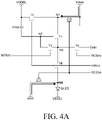
- FIG. 4A is a circuit diagram of a pixel of an organic light emitting display device during an on bias stress period according to an exemplary embodiment of the present disclosure.
- FIG. 4B is a circuit diagram of a pixel of an organic light emitting display device during an initial period according to an exemplary embodiment of the present disclosure.
- FIG. 4C is a circuit diagram of a pixel of an organic light emitting display device during a sampling period according to an exemplary embodiment of the present disclosure.
- FIG. 4D is a circuit diagram of a pixel of an organic light emitting display device during an emission period according to an exemplary embodiment of the present disclosure.
- the organic light emitting display device may be driven to be divided into a refresh frame and an anode reset frame.
- the data voltage Vdata is programmed in each pixel P and the organic light emitting diode OLED emits light.
- the anode reset frame may be a vertical blank frame and the anode electrode of the organic light emitting diode OLED is reset during the anode reset frame.
- the anode reset frame may include a plurality of on bias stress periods (hereinafter, referred to as "stress periods").
- the stress period (on bias stress) is a period in which a bias stress is applied to the first node N1 which is the source electrode of the driving transistor T1.
- the anode electrode of the organic light emitting diode OLED may be reset.
- the reset voltage VAR is a low level and the initialization voltage Vini and the data voltage Vdata are high levels.
- the refresh frame may be divided into an initial period, a sampling period, and an emission period.
- the initial period is a period in which the voltage of the third node N3 which is the drain electrode of the driving transistor T1 is initialized.
- the sampling period is a period in which a threshold voltage Vth of the driving transistor T1 is sampled and the data voltage Vdata is programmed.
- the emission period is a period in which the organic light emitting diode OLED emits light in accordance with the driving current by the source-gate voltage of the programmed driving transistor T1. As illustrated in FIG. 3 , during the refresh frame, the reset voltage VAR and the initialization voltage Vini are low levels.
- the second scan signal SC2(n) is a low level which is a turn on level. That is, during the stress period (on bias stress) of the anode reset frame, an odd-numbered second scan signal SC2_Odd(n) is a low level which is a turn on level and an even-numbered second scan signal SC2_Even(n) is a low level which is a turn on level.
- the odd-numbered second scan signal SC2_Odd(n) and the even-numbered second scan signal SC2_Even(n) which are second scan signals SC2(n) may have a waveform including a plurality of pulses.
- the data voltage Vdata is always a high level.
- the seventh transistor T7 is turned on to apply the reset voltage VAR to the fourth node N4. That is, the anode electrode of the organic light emitting diode OLED is reset to the reset voltage VAR.
- the second transistor T2 is turned on to apply a high level of data voltage Vdata to the first node N1.
- the high level of data voltage Vdata may be selected in a voltage range which is sufficiently higher than an operating voltage of the organic light emitting diode OLED and may be set to a voltage equal to or less than a high potential driving voltage VDDEL. That is, during the stress period (on bias stress), the on bias stress is applied to the first node N1 which is the source electrode of the driving transistor T1 to drop the gate-source voltage Vgs of the driving transistor T1. Accordingly, during the stress period (on bias stress), the source-drain current Ids of the driving transistor T1 flows to relieve the hysteresis of the driving transistor T1.
- the initialization voltage Vini may be a high level. Therefore, a high level of third scan signal SC3(n) is applied to the gate electrode of the fourth transistor T4 and a high level of initialization voltage Vini is applied to the source electrode of the fourth transistor T4 so that a potential difference between the gate electrode and the source electrode of the fourth transistor T4 may be reduced. Accordingly, during the anode reset frame, the leakage current of the fourth transistor T4 may be reduced.
- the first scan signal SC1(n) is a high level which is a turn on level and the third scan signal SC3(n) is a low level which is a turn on level. Therefore, the third transistor T3 and the fourth transistor T4 are turned on to apply the initialization voltage Vini to the third node N3 and the second node N2. As a result, the gate electrode and the drain electrode of the driving transistor T1 are initialized to the initialization voltage Vini.
- the initialization voltage Vini may be selected in a voltage range which is sufficiently less than an operating voltage of the organic light emitting diode OLED and may be set to a voltage equal to or less than a low potential driving voltage VSSEL.
- the first scan signal SC1(n) is a high level which is a turn on level and the second scan signal SC2(n) is a low level which is a turn on level.
- the first scan signal SC1(n) is a high level which is a turn on level
- an odd-numbered second scan signal SC2_Odd(n) is a low level which is a turn on level
- an even-numbered second scan signal SC2_Even(n) is a low level which is a turn on level.
- the odd-numbered second scan signal SC2_Odd(n) and the even-numbered second scan signal SC2_Even(n) which are second scan signals SC2(n) are illustrated by a waveform including one pulse.
- the present disclosure is not limited thereto and the odd-numbered second scan signal SC2_Odd(n) and the even-numbered second scan signal SC2_Even(n) which are second scan signals SC2(n) may have a waveform including a plurality of pulses.
- the second transistor T2 is turned on so that the data voltage Vdata is applied to the first node N1.
- the third transistor T3 is also turned on so that the driving transistor T1 forms a diode connection. Therefore, the gate electrode and the drain electrode of the driving transistor T1 are shorted so that the driving transistor T1 operates as a diode.
- a current Ids flows between the source and the drain of the driving transistor T1.
- the gate electrode and the drain electrode of the driving transistor T1 are diode-connected, so that the voltage of the second node N2 rises by the current flowing from the source electrode to the drain electrode until the gate-source voltage Vgs of the driving transistor T1 becomes Vth.
- the voltage of the second node N2 is charged with a voltage Vdata-
- the second scan signal SC2(n) is a low level which is a turn on level, so that the seventh transistor T7 is turned on to apply the reset voltage VAR to the fourth node N4. That is, the anode electrode of the organic light emitting diode OLED is reset to the reset voltage VAR.
- the second transistor T2 is turned on to apply the data voltage Vdata to the first node N1. Therefore, also in the refresh frame, the bias stress is applied to the first node N1 which is the source electrode of the driving transistor T1 to relieve the hysteresis of the driving transistor T1.
- the emission signal EM(n) is a low level which is a turn on level. Therefore, the fifth transistor T5 is turned on to apply the high potential driving voltage VDDEL to the first node N1.
- the sixth transistor T6 is also turned on to form a current path of the third node N3 and the fourth node N4. As a result, a driving current Ioled passing through the source electrode and the drain electrode of the driving transistor T1 is applied to the organic light emitting diode OLED.
- Equation 1 A relational expression of the driving current Ioled flowing through the organic light emitting diode OLED during the emission period is represented by the following Equation 1.
- Equation 1 k/2 is a proportional constant determined by an electron mobility of the driving transistor T1, a parasitic capacitance, a channel capacity, and the like.
- Equation 1 it is understood that in the relational expression of the driving current Ioled, a component of the threshold voltage Vth of the driving transistor T1 is eliminated so that even though in the display device of the present disclosure, the threshold voltage Vth changes, the driving current Ioled does not change.
- the display device of the present disclosure may program the data voltage regardless of the variation of the threshold voltage Vth during the sampling period.
- the anode electrode of the organic light emitting diode OLED is reset to the reset voltage VAR in both the stress period of the anode reset frame and the sampling period of the refresh frame.
- the anode electrode of the organic light emitting diode OLED may be periodically reset during the refresh frame and the reset frame. Accordingly, the consistent rising of the voltage of the anode electrode of the organic light emitting diode OLED due to the leakage current is suppressed even in the driving at a low frequency so that the anode electrode of the organic light emitting diode OLED may maintain a constant voltage level. Accordingly, even though the driving frequency is switched to a low frequency, the luminance variance of the organic light emitting display device is reduced so that the image quality may be increased.
- FIG. 5 is a view illustrating a gate driver of an organic light emitting display device according to an exemplary embodiment of the present disclosure.
- a separate stage which swings an initialization voltage may be included in the gate driver to increase the initialization voltage from a low level to a high level even in one frame.
- the organic light emitting display device includes a separate stage which swings the initialization voltage, which results in the increase of the bezel and when the separate stage is driven, the power consumption may also be increased.
- the organic light emitting display device uses a high level of data voltage Vdata to apply the on bias stress to the driving transistor T1. Accordingly, the organic light emitting display device according to the exemplary embodiment of the present disclosure does not need to include a separate stage which swings the initialization voltage in the gate driver to apply the on bias stress.
- both the first gate driver 401 disposed at the left side of the display area A/A and the second gate driver 402 disposed at the right side of the display area A/A include only two emission signal stages EM, a first scan signal stage SC1, an odd-numbered second scan signal stage SC2_Odd, an even-numbered second scan signal stage SC2_Even, and a third scan signal stage SC3.
- the first gate driver 401 and the second gate driver 402 may not include a separate stage which swings the initialization voltage to apply the on bias stress.
- a width of each of the first gate driver 401 and the second gate driver 402 may be reduced from 400 ⁇ m to 350 ⁇ m so that the width of the bezel may be reduced. Further, there is no need to drive a separate stage for applying the on bias stress, so that the power consumption may also be reduced.
- the organic light emitting display device According to the exemplary embodiment of the present disclosure, there is no need to form a separate stage for applying the on bias stress, so that the manufacturing process yield of the gate driver may be improved.
- an organic light emitting display device according to another exemplary embodiment of the present disclosure will be described.
- the difference of an organic light emitting display device is only the fourth transistor and the initialization voltage, but other technical features are the same.
- FIG. 6 is a circuit diagram illustrating a pixel of an organic light emitting display device according to another exemplary embodiment of the present disclosure.
- Each pixel P includes an organic light emitting diode OLED, a driving transistor T1, second to seventh transistors T2 to T7, and a storage capacitor Cstg.
- the organic light emitting diode OLED emits light by a driving current supplied from the driving transistor T1.
- a multilayered organic compound layer is formed between the anode electrode and the cathode electrode of the organic light emitting diode OLED.
- the organic compound layer includes at least one of a hole transfer layer and an electron transfer layer, and an emission layer (EML).
- the hole transfer layer is a layer which injects or transfers holes to the emission layer and for example, may include a hole injection layer (HIL), a hole transport layer (HTL), and an electron blocking layer (EBL).
- the electron transfer layer is a layer which injects or transfers the electrons to the emission layer and for example, may include an electron transport layer (ETL), an electron injection layer (EIL), and a hole blocking layer (HBL).
- An anode electrode of the organic light emitting diode OLED is connected to a fourth node N4 and a cathode electrode of the organic light emitting diode is connected to an input terminal of a low potential driving
- the driving transistor T1 controls a driving current applied to the organic light emitting diode OLED in accordance with a source-gate voltage Vsg.
- the driving transistor T1 may be a p-type MOSFET (PMOS) and a low temperature polycrystalline silicon (LTPS) thin film transistor.
- a source electrode of the driving transistor T1 is connected to a first node N1, a gate electrode is connected to a second node N2, and a drain electrode is connected to a third node N3.
- the driving transistor T1 may be referred to as a first transistor.
- the second transistor T2 applies a data voltage Vdata supplied from a data line to a first node N1 which is the source electrode of the driving transistor T1.
- the second transistor T2 may be a p-type MOSFET (PMOS) and a low temperature polycrystalline silicon (LTPS) thin film transistor.
- the second transistor T2 includes a source electrode connected to the data line, a drain electrode connected to the first node N1, and a gate electrode connected to a second scan signal line which transmits a second scan signal SC2(n). Accordingly, the second transistor T2 applies a data voltage Vdata supplied from the data line to the first node N1 which is the source electrode of the driving transistor T1, in response to a low level of second scan signal SC2(n) which is a turn on level.
- the third transistor T3 forms a diode connection between a gate electrode and a drain electrode of the driving transistor T1.
- the third transistor T3 may be an n-type MOSFET NMOS and an oxide thin film transistor to reduce a leakage current.
- the third transistor T3 includes a drain electrode connected to the third node N3, a source electrode connected to the second node N2, and a gate electrode connected to a first scan signal line which transmits a first scan signal SC1(n). Therefore, the third transistor T3 forms a diode connection between the gate electrode and the drain electrode of the driving transistor T1 in response to a high level of the first scan signal SC1(n) which is a turn on level.
- the fourth transistor T4 applies an initialization voltage Vini to the third node N3 which is the drain electrode of the driving transistor T1.
- the fourth transistor T4 may be an n-type MOSFET (NMOS) and an oxide thin film transistor to reduce a leakage current.
- the fourth transistor T4 includes a source electrode connected to an initialization voltage line which transmits an initialization voltage Vini, a drain electrode connected to the third node N3, and a gate electrode connected to a first scan signal line of a previous stage which transmits a first scan signal SC1(n - 1) of the previous stage. Accordingly, the fourth transistor T4 applies the initialization voltage Vini to the third node N3 which is the drain electrode of the driving transistor T1, in response to a high level of first scan signal SC1(n - 1) of the previous stage which is a turn on level.
- the fifth transistor T5 applies a high potential driving voltage VDDEL to the first node N1 which is the source electrode of the driving transistor T1.
- the fifth transistor T5 may be a p-type MOSFET (PMOS) and a low temperature polycrystalline silicon (LTPS) thin film transistor.
- the fifth transistor T5 includes a source electrode connected to a high potential driving voltage line which transmits a high potential driving voltage VDDEL, a drain electrode connected to the first node N1, and a gate electrode connected to an emission signal line which transmits an emission signal EM(n). Accordingly, the fifth transistor T5 applies the high potential driving voltage VDDEL to the first node N1 which is the source electrode of the driving transistor T1, in response to a low level of emission signal EM(n) which is a turn on level.
- the sixth transistor T6 forms a current path between the driving transistor T1 and the organic light emitting diode OLED.
- the sixth transistor T6 may be a p-type MOSFET (PMOS) and a low temperature polycrystalline silicon (LTPS) thin film transistor.
- the sixth transistor T6 includes a source electrode connected to the third node N3, a drain electrode connected to the fourth node N4, and a gate electrode connected to the emission signal line which transmits an emission signal EM(n).
- the sixth transistor T6 forms a current path between the third node N3 which is the source electrode of the sixth transistor T6 and the fourth node N4 which is the drain electrode of the sixth transistor T6, in response to the emission signal EM(n). Accordingly, the sixth transistor T6 forms a current path between the driving transistor T1 and the organic light emitting diode OLED in response to a low level of emission signal EM(n) which is a turn on level.
- the seventh transistor T7 applies a reset voltage VAR to the fourth anode N4 which is an anode of the organic light emitting diode.
- the seventh transistor T7 may be a p-type MOSFET (PMOS) and a low temperature polycrystalline silicon (LTPS) thin film transistor.
- the seventh transistor T7 includes a source electrode connected to the reset voltage line which transmits the reset voltage VAR, a drain electrode connected to the fourth node N4, and a gate electrode connected to a second scan signal line which transmits a second scan signal SC2(n). Accordingly, the seventh transistor T7 applies the reset voltage VAR to the fourth node N4 which is the anode of the light emitting diode, in response to a low level of second scan signal SC2(n) which is a turn on level.
- PMOS p-type MOSFET
- LTPS low temperature polycrystalline silicon
- the storage capacitor Cstg holds a data voltage Vdata stored in each pixel for one frame.
- the storage capacitor Cstg includes a first electrode connected to the second node N2 and a second electrode connected to the high potential driving voltage line which transmits a high potential driving voltage VDDEL. That is, one electrode of the storage capacitor Cstg is connected to the gate electrode of the driving transistor T1 and the other electrode of the storage capacitor Cstg is connected to the high potential driving voltage line which transmits a high potential driving voltage VDDEL.
- FIG. 7 is a waveform illustrating a signal which is applied to a pixel of an organic light emitting display device during one frame according to another exemplary embodiment of the present disclosure.
- FIG. 8A is a circuit diagram of a pixel of an organic light emitting display device during an on bias stress period according to another exemplary embodiment of the present disclosure.
- FIG. 8B is a circuit diagram of a pixel of an organic light emitting display device during an initial period according to another exemplary embodiment of the present disclosure.
- FIG. 8C is a circuit diagram of a pixel of an organic light emitting display device during a sampling period according to another exemplary embodiment of the present disclosure.
- FIG. 8D is a circuit diagram of a pixel of an organic light emitting display device during an emission period according to another exemplary embodiment of the present disclosure.
- the organic light emitting display device may also be driven to be divided into a refresh frame and an anode reset frame.
- the data voltage Vdata is programmed in each pixel P and the organic light emitting diode OLED emits light.
- the anode reset frame may be a vertical blank frame and the anode electrode of the organic light emitting diode OLED is reset during the anode reset frame.
- the anode reset frame may include a plurality of stress periods (on bias stress).
- the stress period (on bias stress) is a period in which a bias stress is applied to the first node N1 which is the source electrode of the driving transistor T1.
- the anode electrode of the organic light emitting diode OLED may be reset.
- the reset voltage VAR and the initialization voltage Vini are low levels and the data voltage Vdata is a high level.
- the refresh frame may be divided into an initial period, a sampling period, and an emission period.
- the initial period is a period in which the voltage of the third node N3 which is the drain electrode of the driving transistor T1 is initialized.
- the sampling period is a period in which a threshold voltage Vth of the driving transistor T1 is sampled and the data voltage Vdata is programmed.
- the emission period is a period in which the organic light emitting diode OLED emits light in accordance with the driving current by the source-gate voltage of the programmed driving transistor T1. As illustrated in FIG. 7 , during the refresh frame, the reset voltage VAR and the initialization voltage Vini are low levels.
- the second scan signal SC2(n) is a low level which is a turn on level. That is, during the stress period (on bias stress) of the anode reset frame, an odd-numbered second scan signal SC2_Odd(n) is a low level which is a turn on level and an even-numbered second scan signal SC2_Even(n) is a low level which is a turn on level.
- the odd-numbered second scan signal SC2_Odd(n) and the even-numbered second scan signal SC2_Even(n) which are second scan signals SC2(n) may have a waveform including a plurality of pulses.
- the data voltage Vdata is always a high level.
- the seventh transistor T7 is turned on to apply the reset voltage VAR to the fourth node N4. That is, the anode electrode of the organic light emitting diode OLED is reset to the reset voltage VAR.
- the second transistor T2 is turned on to apply a high level of data voltage Vdata to the first node N1.
- the high level of data voltage Vdata may be selected in a voltage range which is sufficiently higher than an operating voltage of the organic light emitting diode OLED and may be set to a voltage equal to or less than a high potential driving voltage VDDEL. That is, during the stress period (on bias stress), the on bias stress is applied to the first node N1 which is the source electrode of the driving transistor T1 to drop the gate-source voltage Vgs of the driving transistor T1. Accordingly, during the stress period (on bias stress), the source-drain current Ids of the driving transistor T1 flows to relieve the hysteresis of the driving transistor T1.
- the first scan signal SC1(n) is a high level which is a turn on level and the first scan signal SC1(n - 1) of the previous stage is a high level which is a turn on level. Therefore, the third transistor T3 and the fourth transistor T4 are turned on to apply the initialization voltage Vini to the third node N3 and the second node N2. As a result, the gate electrode and the drain electrode of the driving transistor T1 are initialized to the initialization voltage Vini.
- the initialization voltage Vini may be selected in a voltage range which is sufficiently less than an operating voltage of the organic light emitting diode OLED and may be set to a voltage equal to or less than a low potential driving voltage VSSEL.
- the first scan signal SC1(n) is a high level which is a turn on level and the second scan signal SC2(n) is a low level which is a turn on level.
- the first scan signal SC1(n) is a high level which is a turn on level
- an odd-numbered second scan signal SC2_Odd(n) is a low level which is a turn on level
- an even-numbered second scan signal SC2_Even(n) is a low level which is a turn on level.
- the odd-numbered second scan signal SC2_Odd(n) and the even-numbered second scan signal SC2_Even(n) which are second scan signals SC2(n) are illustrated by a waveform including one pulse.
- the present disclosure is not limited thereto and the odd-numbered second scan signal SC2_Odd(n) and the even-numbered second scan signal SC2_Even(n) which are second scan signals SC2(n) may have a waveform including a plurality of pulses.
- the second transistor T2 is turned on so that the data voltage Vdata is applied to the first node N1.
- the third transistor T3 is also turned on so that the driving transistor T1 is diode-connected. Therefore, the gate electrode and the drain electrode of the driving transistor T1 are shorted so that the driving transistor T1 operates as a diode.
- a current Ids flows between the source and the drain of the driving transistor T1.
- the gate electrode and the drain electrode of the driving transistor T1 are diode-connected, so that the voltage of the second node N2 rises by the current flowing from the source electrode to the drain electrode until the gate-source voltage Vgs of the driving transistor T1 becomes Vth.
- the voltage of the second node N2 is charged with a voltage Vdata-
- the second scan signal SC2(n) is a low level which is a turn on level, so that the seventh transistor T7 is turned on to apply the reset voltage VAR to the fourth node N4. That is, the anode electrode of the organic light emitting diode OLED is reset to the reset voltage VAR.
- the second transistor T2 is turned on to apply the data voltage Vdata to the first node N1. Therefore, also in the refresh frame, the bias stress is applied to the first node N1 which is the source electrode of the driving transistor T1 to relieve the hysteresis of the driving transistor T1.
- the emission signal EM(n) is a low level which is a turn on level. Therefore, the fifth transistor T5 is turned on to apply the high potential driving voltage VDDEL to the first node N1.
- the sixth transistor T6 is also turned on to form a current path of the third node N3 and the fourth node N4. As a result, a driving current Ioled passing through the source electrode and the drain electrode of the driving transistor T1 is applied to the organic light emitting diode OLED.
- Equation 1 A relational expression of the driving current Ioled flowing through the organic light emitting diode OLED during the emission period is represented by the above-described Equation 1.
- Equation 1 it is understood that in the relational expression of the driving current Ioled, a component of the threshold voltage Vth of the driving transistor T1 is eliminated so that even though in the display device of the present disclosure, the threshold voltage Vth changes, the driving current Ioled does not change.
- the display device of the present disclosure may program the data voltage regardless of the variation of the threshold voltage Vth during the sampling period.
- the anode electrode of the organic light emitting diode OLED is reset to the reset voltage VAR in both the stress period of the anode reset frame and the sampling period of the refresh frame.
- the anode electrode of the organic light emitting diode OLED may be periodically reset during the refresh frame and the reset frame. Accordingly, the consistent rising of the voltage of the anode electrode of the organic light emitting diode OLED due to the leakage current is suppressed even in the driving at a low frequency so that the anode electrode of the organic light emitting diode OLED may maintain a constant voltage level. Accordingly, even though the driving frequency is switched to a low frequency, the luminance variance of the organic light emitting display device is reduced so that the image quality may be increased.
- FIG. 9 is a view illustrating a gate driver of an organic light emitting display device according to another exemplary embodiment of the present disclosure.
- the organic light emitting display device uses a high level of data voltage Vdata to apply the on bias stress to the driving transistor T1. Accordingly, the organic light emitting display device according to another exemplary embodiment of the present disclosure does not need to include a separate stage which swings the initialization voltage in the gate driver to apply the on bias stress.
- the first gate driver 401 disposed at the left side of the display area A/A includes only the emission signal stage EM, an odd-numbered second scan signal stage SC2_Odd and an even-numbered second scan signal stage SC2_Even
- the second gate driver 402 disposed at the right side of the display area A/A include only a first scan signal stage SC1, an odd-numbered second scan signal stage SC2_Odd and an even-numbered second scan signal stage SC2_Even.
- the first gate driver 401 and the second gate driver 402 may not include a third scan signal stage.
- a width of each of the first gate driver 401 and the second gate driver 402 may be reduced from 350 ⁇ m to 300 ⁇ m as compared with the organic light emitting display device according to the exemplary embodiment of the present disclosure so that the width of the bezel may be further reduced. Further, there is no need to drive a third scan signal stage, so that the power consumption may also be reduced.
- an organic light emitting display device according to still another exemplary embodiment (Example 3) of the present disclosure will be described. Only difference between an organic light emitting display device according to still another exemplary embodiment (Example 3) of the present disclosure and the organic light emitting display device according to the exemplary embodiment of the present disclosure is a drain electrode connection relationship of the fourth transistor. Other technical features are the same. Therefore, a signal applied to a pixel of the organic light emitting display device according to still another exemplary embodiment (Example 3) of the present disclosure and a signal applied to a pixel of the organic light emitting display device according to the exemplary embodiment of the present disclosure are the same. Therefore, the organic light emitting display device according to still another exemplary embodiment (Example 3) of the present disclosure will be described using a waveform of FIG. 3 .
- FIG. 10 is a circuit diagram illustrating a pixel of an organic light emitting display device according to still another exemplary embodiment (Example 3) of the present disclosure.
- Each pixel P includes an organic light emitting diode OLED, a driving transistor T1, second to seventh transistors T2 to T7, and a storage capacitor Cstg.
- the organic light emitting diode OLED emits light by a driving current supplied from the driving transistor T1.
- a multilayered organic compound layer is formed between the anode electrode and the cathode electrode of the organic light emitting diode OLED.
- the organic compound layer includes at least one of a hole transfer layer and an electron transfer layer, and an emission layer (EML).
- the hole transfer layer is a layer which injects or transfers holes to the emission layer and for example, may include a hole injection layer (HIL), a hole transport layer (HTL), and an electron blocking layer (EBL).
- the electron transfer layer is a layer which injects or transfers the electrons to the emission layer and for example, may include an electron transport layer (ETL), an electron injection layer (EIL), and a hole blocking layer (HBL).
- An anode electrode of the organic light emitting diode OLED is connected to a fourth node N4 and a cathode electrode of the organic light emitting diode is connected to an input terminal of a low potential driving
- the driving transistor T1 controls a driving current applied to the organic light emitting diode OLED in accordance with a source-gate voltage Vsg.
- the driving transistor T1 may be a p-type MOSFET (PMOS) and a low temperature polycrystalline silicon (LTPS) thin film transistor.
- a source electrode of the driving transistor T1 is connected to a first node N1, a gate electrode is connected to a second node N2, and a drain electrode is connected to a third node N3.
- the driving transistor T1 may be referred to as a first transistor.
- the second transistor T2 applies a data voltage Vdata supplied from a data line to a first node N1 which is the source electrode of the driving transistor T1.
- the second transistor T2 may be a p-type MOSFET (PMOS) and a low temperature polycrystalline silicon (LTPS) thin film transistor.
- the second transistor T2 includes a source electrode connected to the data line, a drain electrode connected to the first node N1, and a gate electrode connected to a second scan signal line which transmits a second scan signal SC2(n). Accordingly, the second transistor T2 applies a data voltage Vdata supplied from the data line to the first node N1 which is the source electrode of the driving transistor T1, in response to a low level of second scan signal SC2(n) which is a turn on level.
- the third transistor T3 forms a diode connection between a gate electrode and a drain electrode of the driving transistor T1.
- the third transistor T3 may be an n-type MOSFET NMOS and an oxide thin film transistor to reduce a leakage current.
- the third transistor T3 includes a drain electrode connected to the third node N3, a source electrode connected to the second node N2, and a gate electrode connected to a first scan signal line which transmits a first scan signal SC1(n). Therefore, the third transistor T3 forms a diode connection between the gate electrode and the drain electrode of the driving transistor T1 in response to the first scan signal SC1(n) of a high level which is a turn on level.
- the fourth transistor T4 applies an initialization voltage Vini to the second node N2 which is the gate electrode of the driving transistor T1.
- the fourth transistor T4 may be a p-type MOSFET (PMOS) and a low temperature polycrystalline silicon (LTPS) thin film transistor.
- the fourth transistor T4 includes a source electrode connected to an initialization voltage line which transmits an initialization voltage Vini, a drain electrode connected to the second node N2, and a gate electrode connected to a third scan signal line which transmits a third scan signal SC3(n). Accordingly, the fourth transistor T4 applies the initialization voltage Vini to the second node N2 which is the gate electrode of the driving transistor T1, in response to a low level of third scan signal SC3(n) which is a turn on level.
- the fifth transistor T5 applies a high potential driving voltage VDDEL to the first node N1 which is the source electrode of the driving transistor T1.
- the fifth transistor T5 may be a p-type MOSFET (PMOS) and a low temperature polycrystalline silicon (LTPS) thin film transistor.
- the fifth transistor T5 includes a source electrode connected to a high potential driving voltage line which transmits a high potential driving voltage VDDEL, a drain electrode connected to the first node N1, and a gate electrode connected to an emission signal line which transmits an emission signal EM(n). Accordingly, the fifth transistor T5 applies the high potential driving voltage VDDEL to the first node N1 which is the source electrode of the driving transistor T1, in response to a low level of emission signal EM(n) which is a turn on level.
- the sixth transistor T6 forms a current path between the driving transistor T1 and the organic light emitting diode OLED.
- the sixth transistor T6 may be a p-type MOSFET (PMOS) and a low temperature polycrystalline silicon (LTPS) thin film transistor.
- the sixth transistor T6 includes a source electrode connected to the third node N3, a drain electrode connected to the fourth node N4, and a gate electrode connected to the emission signal line which transmits an emission signal EM(n).
- the sixth transistor T6 forms a current path between the third node N3 which is the source electrode of the sixth transistor T6 and the fourth node N4 which is the drain electrode of the sixth transistor T6, in response to the emission signal EM(n). Accordingly, the sixth transistor T6 forms a current path between the driving transistor T1 and the organic light emitting diode OLED in response to a low level of emission signal EM(n) which is a turn on level.
- the seventh transistor T7 applies a reset voltage VAR to the fourth anode N4 which is an anode of the organic light emitting diode.
- the seventh transistor T7 may be a p-type MOSFET (PMOS) and a low temperature polycrystalline silicon (LTPS) thin film transistor.
- the seventh transistor T7 includes a source electrode connected to the reset voltage line which transmits the reset voltage VAR, a drain electrode connected to the fourth node N4, and a gate electrode connected to a second scan signal line which transmits a second scan signal SC2(n). Accordingly, the seventh transistor T7 applies the reset voltage VAR to the fourth node N4 which is the anode of the organic light emitting diode, in response to a low level of second scan signal SC2(n) which is a turn on level.
- PMOS p-type MOSFET
- LTPS low temperature polycrystalline silicon
- the storage capacitor Cstg holds a data voltage Vdata stored in each pixel for one frame.
- the storage capacitor Cstg includes a first electrode connected to the second node N2 and a second electrode connected to the high potential driving voltage line which transmits a high potential driving voltage VDDEL. That is, one electrode of the storage capacitor Cstg is connected to the gate electrode of the driving transistor T1 and the other electrode of the storage capacitor Cstg is connected to the high potential driving voltage line which transmits a high potential driving voltage VDDEL.
- FIG. 11A is a circuit diagram of a pixel of an organic light emitting display device during an on bias stress period according to still another exemplary embodiment (Example 3) of the present disclosure.
- FIG. 11B is a circuit diagram of a pixel of an organic light emitting display device during an initial period according to still another exemplary embodiment (Example 3) of the present disclosure.
- FIG. 11C is a circuit diagram of a pixel of an organic light emitting display device during a sampling period according to still another exemplary embodiment (Example 3) of the present disclosure.
- FIG. 11D is a circuit diagram of a pixel of an organic light emitting display device during an emission period according to still another exemplary embodiment (Example 3) of the present disclosure.
- Example 3 The driving of the pixel of the organic light emitting display device according to still another exemplary embodiment (Example 3) of the present disclosure will be described with reference to FIGS. 10 to 11D , as follows.
- the organic light emitting display device may be driven to be divided into a refresh frame and an anode reset frame.
- the data voltage Vdata is programmed in each pixel P and the organic light emitting diode OLED emits light.
- the anode reset frame may be a vertical blank frame and the anode electrode of the organic light emitting diode OLED is reset during the anode reset frame.
- the anode reset frame may include a plurality of stress periods (on bias stress).
- the stress period (on bias stress) is a period in which a bias stress is applied to the first node N1 which is the source electrode of the driving transistor T1.
- the anode electrode of the organic light emitting diode OLED may be reset.
- the reset voltage VAR is a low level and the initialization voltage Vini and the data voltage Vdata are high levels.
- the refresh frame may be divided into an initial period, a sampling period, and an emission period.
- the initial period is a period in which the voltage of the second node N2 which is the gate electrode of the driving transistor T1 is initialized.
- the sampling period is a period in which a threshold voltage Vth of the driving transistor T1 is sampled and the data voltage Vdata is programmed.
- the emission period is a period in which the organic light emitting diode OLED emits light in accordance with the driving current by the source-gate voltage of the programmed driving transistor T1. As illustrated in FIG. 3 , during the refresh frame, the reset voltage VAR and the initialization voltage Vini are low levels.
- the second scan signal SC2(n) is a low level which is a turn on level. That is, during the stress period (on bias stress) of the anode reset frame, an odd-numbered second scan signal SC2_Odd(n) is a low level which is a turn on level and an even-numbered second scan signal SC2_Even(n) is a low level which is a turn on level.
- the odd-numbered second scan signal SC2_Odd(n) and the even-numbered second scan signal SC2_Even(n) which are second scan signals SC2(n) may have a waveform including a plurality of pulses.
- the data voltage Vdata is always a high level.
- the seventh transistor T7 is turned on to apply the reset voltage VAR to the fourth node N4. That is, the anode electrode of the organic light emitting diode OLED is reset to the reset voltage VAR.
- the second transistor T2 is turned on to apply a high level of data voltage Vdata to the first node N1.
- the high level of data voltage Vdata may be selected in a voltage range which is sufficiently higher than an operating voltage of the organic light emitting diode OLED and may be set to a voltage equal to or less than a high potential driving voltage VDDEL. That is, during the stress period (on bias stress), the on bias stress is applied to the first node N1 which is the source electrode of the driving transistor T1 to drop the gate-source voltage Vgs of the driving transistor T1. Accordingly, during the stress period (on bias stress), the source-drain current Ids of the driving transistor T1 flows to relieve the hysteresis of the driving transistor T1.
- the initialization voltage Vini may be a high level. Therefore, a high level of third scan signal SC3(n) is applied to the gate electrode of the fourth transistor T4 and a high level of initialization voltage Vini is applied to the source electrode of the fourth transistor T4 so that a potential difference between the gate electrode and the source electrode of the fourth transistor T4 may be reduced. Accordingly, during the anode reset frame, the leakage current of the fourth transistor T4 may be reduced.
- the first scan signal SC1(n) is a high level which is a turn on level and the third scan signal SC3(n) is a low level which is a turn on level. Therefore, the third transistor T3 and the fourth transistor T4 are turned on to apply the initialization voltage Vini to the third node N3 and the second node N2. As a result, the gate electrode and the drain electrode of the driving transistor T1 are initialized to the initialization voltage Vini.
- the initialization voltage Vini may be selected in a voltage range which is sufficiently less than an operating voltage of the organic light emitting diode OLED and may be set to a voltage equal to or less than a low potential driving voltage VSSEL.
- the first scan signal SC1(n) is a high level which is a turn on level and the second scan signal SC2(n) is a low level which is a turn on level.
- the first scan signal SC1(n) is a high level which is a turn on level
- an odd-numbered second scan signals SC2_Odd(n) is a low level which is a turn on level
- an even-numbered second scan signal SC2_Even(n) is a low level which is a turn on level.
- the odd-numbered second scan signals SC2_Odd(n) and the even-numbered second scan signals SC2_Even(n) which are second scan signals SC2(n) are illustrated by a waveform including one pulse.
- the present disclosure is not limited thereto and the odd-numbered second scan signal SC2_Odd(n) and the even-numbered second scan signal SC2_Even(n) which are second scan signals SC2(n) may have a waveform including a plurality of pulses.
- the second transistor T2 is turned on so that the data voltage Vdata is applied to the first node N1.
- the third transistor T3 is also turned on so that the driving transistor T1 is diode-connected. Therefore, the gate electrode and the drain electrode of the driving transistor T1 are shorted so that the driving transistor T1 operates as a diode.
- a current Ids flows between the source and the drain of the driving transistor T1.
- the gate electrode and the drain electrode of the driving transistor T1 are diode-connected, so that the voltage of the second node N2 rises by the current flowing from the source electrode to the drain electrode until the gate-source voltage Vgs of the driving transistor T1 becomes Vth.
- the voltage of the second node N2 is charged with a voltage Vdata-
- the second scan signal SC2(n) is a low level which is a turn on level, so that the seventh transistor T7 is turned on to apply the reset voltage VAR to the fourth node N4. That is, the anode electrode of the organic light emitting diode OLED is reset to the reset voltage VAR.
- the second transistor T2 is turned on to apply the data voltage Vdata to the first node N1. Therefore, also in the refresh frame, the bias stress is applied to the first node N1 which is the source electrode of the driving transistor T1 to relieve the hysteresis of the driving transistor T1.
- the emission signal EM(n) is a low level which is a turn on level. Therefore, the fifth transistor T5 is turned on to apply the high potential driving voltage VDDEL to the first node N1.
- the sixth transistor T6 is also turned on to form a current path of the third node N3 and the fourth node N4. As a result, a driving current Ioled passing through the source electrode and the drain electrode of the driving transistor T1 is applied to the organic light emitting diode OLED.
- Equation 1 A relational expression of the driving current Ioled flowing through the organic light emitting diode OLED during the emission period is represented by the above-described Equation 1.
- Equation 1 it is understood that in the relational expression of the driving current Ioled, a component of the threshold voltage Vth of the driving transistor T1 is eliminated so that even though in the display device of the present disclosure, the threshold voltage Vth changes, the driving current Ioled does not change.
- the display device of the present disclosure may program the data voltage regardless of the variation of the threshold voltage Vth during the sampling period.
- the anode electrode of the organic light emitting diode OLED is reset to the reset voltage VAR in both the stress period of the anode reset frame and the sampling period of the refresh frame.
- the anode electrode of the organic light emitting diode OLED may be periodically reset during the refresh frame and the reset frame. Accordingly, the consistent rising of the voltage of the anode electrode of the organic light emitting diode OLED due to the leakage current is suppressed even in the driving at a low frequency so that the anode electrode of the organic light emitting diode OLED may maintain a constant voltage level. Accordingly, even though the driving frequency is switched to a low frequency, the luminance variance of the organic light emitting display device is reduced so that the image quality may be increased.
- the organic light emitting display device uses a high level of data voltage Vdata to apply the on bias stress to the driving transistor T1. Accordingly, the organic light emitting display device according to still another exemplary embodiment (Example 3) of the present disclosure does not need to include a separate stage which swings the initialization voltage in the gate driver to apply the on bias stress.
- both the first gate driver 401 disposed at the left side of the display area A/A and the second gate driver 402 disposed at the right side of the display area A/A include only two emission signal stages EM, a first scan signal stage SC1, an odd-numbered second scan signal stage SC2_Odd, an even-numbered second scan signal stage SC2_Even, and a third scan signal stage SC3.
- the first gate driver 401 and the second gate driver 402 may not include a separate stage which swings the initialization voltage to apply the on bias stress.
- a width of each of the first gate driver 401 and the second gate driver 402 may be reduced from 400 ⁇ m to 350 ⁇ m so that the width of the bezel may be reduced. Further, there is no need to drive a separate stage for applying the on bias stress, so that the power consumption may also be reduced.
- the organic light emitting display device according to still another exemplary embodiment (Example 3) of the present disclosure, there is no need to form a separate stage for the on bias stress, so that the manufacturing process yield of the gate driver may be improved.
- an organic light emitting display device according to still another exemplary embodiment (Example 4) of the present disclosure will be described.
- the difference of an organic light emitting display device according to still another exemplary embodiment (Example 4) of the present disclosure is only the fourth transistor and the initialization voltage, but other technical features are the same. Therefore, a signal applied to a pixel of the organic light emitting display device according to still another exemplary embodiment (Example 4) of the present disclosure and a signal applied to a pixel of the organic light emitting display device according to another exemplary embodiment (Example 2) of the present disclosure are the same. Therefore, the organic light emitting display device according to still another exemplary embodiment (Example 4) of the present disclosure will be described using a waveform of FIG. 7 .
- FIG. 12 is a circuit diagram illustrating a pixel of an organic light emitting display device according to still another exemplary embodiment (Example 4) of the present disclosure.
- Each pixel P includes an organic light emitting diode OLED, a driving transistor T1, second to seventh transistors T2 to T7, and a storage capacitor Cstg.
- the organic light emitting diode OLED emits light by a driving current supplied from the driving transistor T1.
- a multilayered organic compound layer is formed between the anode electrode and the cathode electrode of the organic light emitting diode OLED.
- the organic compound layer includes at least one of a hole transfer layer and an electron transfer layer, and an emission layer (EML).
- the hole transfer layer is a layer which injects or transfers holes to the emission layer and for example, may include a hole injection layer (HIL), a hole transport layer (HTL), and an electron blocking layer (EBL).
- the electron transfer layer is a layer which injects or transfers the electrons to the emission layer and for example, may include an electron transport layer (ETL), an electron injection layer (EIL), and a hole blocking layer (HBL).
- An anode electrode of the organic light emitting diode OLED is connected to a fourth node N4 and a cathode electrode of the organic light emitting diode is connected to an input terminal of a low potential driving
- the driving transistor T1 controls a driving current applied to the organic light emitting diode OLED in accordance with a source-gate voltage Vsg.
- the driving transistor T1 may be a p-type MOSFET (PMOS) and a low temperature polycrystalline silicon (LTPS) thin film transistor.
- a source electrode of the driving transistor T1 is connected to a first node N1, a gate electrode is connected to a second node N2, and a drain electrode is connected to a third node N3.
- the driving transistor T1 may be referred to as a first transistor.
- the second transistor T2 applies a data voltage Vdata supplied from a data line to a first node N1 which is the source electrode of the driving transistor T1.
- the second transistor T2 may be a p-type MOSFET (PMOS) and a low temperature polycrystalline silicon (LTPS) thin film transistor.
- the second transistor T2 includes a source electrode connected to the data line, a drain electrode connected to the first node N1, and a gate electrode connected to a second scan signal line which transmits a second scan signal SC2(n). Accordingly, the second transistor T2 applies a data voltage Vdata supplied from the data line to the first node N1 which is the source electrode of the driving transistor T1, in response to a low level of second scan signal SC2(n) which is a turn on level.
- the third transistor T3 forms a diode connection between a gate electrode and a drain electrode of the driving transistor T1.
- the third transistor T3 may be an n-type MOSFET (NMOS) and an oxide thin film transistor to reduce a leakage current.
- the third transistor T3 includes a drain electrode connected to the third node N3, a source electrode connected to the second node N2, and a gate electrode connected to a first scan signal line which transmits a first scan signal SC1(n). Therefore, the third transistor T3 forms a diode connection between the gate electrode and the drain electrode of the driving transistor T1 in response to a high level of the first scan signal SC1(n) which is a turn on level.
- the fourth transistor T4 applies an initialization voltage Vini to the second node N2 which is the gate electrode of the driving transistor T1.
- the fourth transistor T4 may be an n-type MOSFET (NMOS) and an oxide thin film transistor to reduce a leakage current.
- the fourth transistor T4 includes a source electrode connected to an initialization voltage line which transmits an initialization voltage Vini, a drain electrode connected to the second node N2, and a gate electrode connected to a first scan signal line of a previous stage which transmits a first scan signal SC1(n - 1) of the previous stage. Accordingly, the fourth transistor T4 applies the initialization voltage Vini to the second node N2 which is the gate electrode of the driving transistor T1, in response to a high level of first scan signal SC1(n - 1) of the previous stage which is a turn on level.
- the fifth transistor T5 applies a high potential driving voltage VDDEL to the first node N1 which is the source electrode of the driving transistor T1.
- the fifth transistor T5 may be a p-type MOSFET (PMOS) and a low temperature polycrystalline silicon (LTPS) thin film transistor.
- the fifth transistor T5 includes a source electrode connected to a high potential driving voltage line which transmits a high potential driving voltage VDDEL, a drain electrode connected to the first node N1, and a gate electrode connected to an emission signal line which transmits an emission signal EM(n). Accordingly, the fifth transistor T5 applies the high potential driving voltage VDDEL to the first node N1 which is the source electrode of the driving transistor T1, in response to a low level of emission signal EM(n) which is a turn on level.
- the sixth transistor T6 forms a current path between the driving transistor T1 and the organic light emitting diode OLED.
- the sixth transistor T6 may be a p-type MOSFET (PMOS) and a low temperature polycrystalline silicon (LTPS) thin film transistor.
- the sixth transistor T6 includes a source electrode connected to the third node N3, a drain electrode connected to the fourth node N4, and a gate electrode connected to the emission signal line which transmits an emission signal EM(n).
- the sixth transistor T6 forms a current path between the third node N3 which is the source electrode of the sixth transistor T6 and the fourth node N4 which is the drain electrode of the sixth transistor T6, in response to the emission signal EM(n). Accordingly, the sixth transistor T6 forms a current path between the driving transistor T1 and the organic light emitting diode OLED in response to a low level of emission signal EM(n) which is a turn on level.
- the seventh transistor T7 applies a reset voltage VAR to the fourth anode N4 which is an anode of the organic light emitting diode.
- the seventh transistor T7 may be a p-type MOSFET (PMOS) and a low temperature polycrystalline silicon (LTPS) thin film transistor.
- the seventh transistor T7 includes a source electrode connected to the reset voltage line which transmits the reset voltage VAR, a drain electrode connected to the fourth node N4, and a gate electrode connected to a second scan signal line which transmits a second scan signal SC2(n). Accordingly, the seventh transistor T7 applies the reset voltage VAR to the fourth node N4 which is the anode of the organic light emitting diode, in response to a low level of second scan signal SC2(n) which is a turn on level.
- PMOS p-type MOSFET
- LTPS low temperature polycrystalline silicon
- the storage capacitor Cstg holds a data voltage Vdata stored in each pixel for one frame.
- the storage capacitor Cstg includes a first electrode connected to the second node N2 and a second electrode connected to the high potential driving voltage line which transmits a high potential driving voltage VDDEL. That is, one electrode of the storage capacitor Cstg is connected to the gate electrode of the driving transistor T1 and the other electrode of the storage capacitor Cstg is connected to the high potential driving voltage line VDL which transmits a high potential driving voltage VDDEL.
- FIG. 13A is a circuit diagram of a pixel of an organic light emitting display device during an on bias stress period according to still another exemplary embodiment (Example 4) of the present disclosure.
- FIG. 13B is a circuit diagram of a pixel of an organic light emitting display device during an initial period according to still another exemplary embodiment (Example 4) of the present disclosure.
- FIG. 13C is a circuit diagram of a pixel of an organic light emitting display device during a sampling period according to still another exemplary embodiment (Example 4) of the present disclosure.
- FIG. 13D is a circuit diagram of a pixel of an organic light emitting display device during an emission period according to still another exemplary embodiment (Example 4) of the present disclosure.
- Example 4 The driving of the pixel of the organic light emitting display device according to still another exemplary embodiment (Example 4) of the present disclosure will be described with reference to FIGS. 12 to 13D , as follows.
- the organic light emitting display device may be driven to be divided into a refresh frame and an anode reset frame.
- the data voltage Vdata is programmed in each pixel P and the organic light emitting diode OLED emits light.
- the anode reset frame may be a vertical blank frame and the anode electrode of the organic light emitting diode OLED is reset during the anode reset frame.
- the anode reset frame may include a plurality of stress periods (on bias stress).
- the stress period (on bias stress) is a period in which a bias stress is applied to the first node N1 which is the source electrode of the driving transistor T1. Further, during the stress period, the anode electrode of the organic light emitting diode OLED may be reset. Further, as illustrated in FIG. 7 , during the anode reset frame, the reset voltage VAR and the initialization voltage Vini are low levels and the data voltage Vdata is a high level.
- the refresh frame may be divided into an initial period, a sampling period, and an emission period.
- the initial period is a period in which the voltage of the second node N2 which is the gate electrode of the driving transistor T1 is initialized.
- the sampling period is a period in which a threshold voltage Vth of the driving transistor T1 is sampled and the data voltage Vdata is programmed.
- the emission period is a period in which the organic light emitting diode OLED emits light in accordance with the driving current by the source-gate voltage of the programmed driving transistor T1. As illustrated in FIG. 7 , during the refresh frame, the reset voltage VAR and the initialization voltage Vini are low levels.
- the second scan signal SC2(n) is a low level which is a turn on level. That is, during the stress period (on bias stress) of the anode reset frame, an odd-numbered second scan signal SC2_Odd(n) is a low level which is a turn on level and an even-numbered second scan signal SC2_Even(n) is a low level which is a turn on level.
- the odd-numbered second scan signal SC2_Odd(n) and the even-numbered second scan signal SC2_Even(n) which are second scan signals SC2(n) may have a waveform including a plurality of pulses.
- the data voltage Vdata is always a high level.
- the seventh transistor T7 is turned on to apply the reset voltage VAR to the fourth node N4. That is, the anode electrode of the organic light emitting diode OLED is reset to the reset voltage VAR.
- the second transistor T2 is turned on to apply a high level of data voltage Vdata to the first node N1.
- the high level of data voltage Vdata may be selected in a voltage range which is sufficiently higher than an operating voltage of the organic light emitting diode OLED and may be set to a voltage equal to or less than a high potential driving voltage VDDEL. That is, during the stress period (on bias stress), the on bias stress is applied to the first node N1 which is the source electrode of the driving transistor T1 to drop the gate-source voltage Vgs of the driving transistor T1. Accordingly, during the stress period (on bias stress), the source-drain current Ids of the driving transistor T1 flows to relieve the hysteresis of the driving transistor T1.
- the first scan signal SC1(n) is a high level which is a turn on level and the first scan signal SC1(n - 1) of the previous stage is a high level which is a turn on level. Therefore, the third transistor T3 and the fourth transistor T4 are turned on to apply the initialization voltage Vini to the third node N3 and the second node N2. As a result, the gate electrode and the drain electrode of the driving transistor T1 are initialized to the initialization voltage Vini.
- the initialization voltage Vini may be selected in a voltage range which is sufficiently less than an operating voltage of the organic light emitting diode OLED and may be set to a voltage equal to or less than a low potential driving voltage VSSEL.
- the first scan signal SC1(n) is a high level which is a turn on level and the second scan signal SC2(n) is a low level which is a turn on level.
- the first scan signal SC1(n) is a high level which is a turn on level
- an odd-numbered second scan signal SC2_Odd(n) is a low level which is a turn on level
- an even-numbered second scan signal SC2_Even(n) is a low level which is a turn on level.
- the odd-numbered second scan signals SC2_Odd(n) and the even-numbered second scan signals SC2_Even(n) which are second scan signals SC2(n) are illustrated by a waveform including one pulse.
- the present disclosure is not limited thereto and the odd-numbered second scan signals SC2_Odd(n) and the even-numbered second scan signals SC2_Even(n) which are second scan signals SC2(n) may have a waveform including a plurality of pulses.
- the second transistor T2 is turned on so that the data voltage Vdata is applied to the first node N1.
- the third transistor T3 is also turned on so that the driving transistor T1 is diode-connected. Therefore, the gate electrode and the drain electrode of the driving transistor T1 are shorted so that the driving transistor T1 operates as a diode.
- a current Ids flows between the source and the drain of the driving transistor T1.
- the gate electrode and the drain electrode of the driving transistor T1 are diode-connected, so that the voltage of the second node N2 rises by the current flowing from the source electrode to the drain electrode until the gate-source voltage Vgs of the driving transistor T1 becomes Vth.
- the voltage of the second node N2 is charged with a voltage Vdata-
- the second scan signal SC2(n) is a low level which is a turn on level, so that the seventh transistor T7 is turned on to apply the reset voltage VAR to the fourth node N4. That is, the anode electrode of the organic light emitting diode OLED is reset to the reset voltage VAR.
- the second transistor T2 is turned on to apply the data voltage Vdata to the first node N1. Therefore, also in the refresh frame, the bias stress is applied to the first node N1 which is the source electrode of the driving transistor T1 to relieve the hysteresis of the driving transistor T1.
- the emission signal EM(n) is a low level which is a turn on level. Therefore, the fifth transistor T5 is turned on to apply the high potential driving voltage VDDEL to the first node N1.
- the sixth transistor T6 is also turned on to form a current path of the third node N3 and the fourth node N4. As a result, a driving current Ioled passing through the source electrode and the drain electrode of the driving transistor T1 is applied to the organic light emitting diode OLED.
- Equation 1 A relational expression of the driving current Ioled flowing through the organic light emitting diode OLED during the emission period is represented by the above-described Equation 1.
- Equation 1 it is understood that in the relational expression of the driving current Ioled, a component of the threshold voltage Vth of the driving transistor T1 is eliminated so that even though in the display device of the present disclosure, the threshold voltage Vth changes, the driving current Ioled does not change.
- the display device of the present disclosure may program the data voltage regardless of the variation of the threshold voltage Vth during the sampling period.
- the anode electrode of the organic light emitting diode OLED is reset to the reset voltage VAR in both the stress period of the anode reset frame and the sampling period of the refresh frame.
- the anode electrode of the organic light emitting diode OLED may be periodically reset during the refresh frame and the reset frame. Accordingly, the consistent rising of the voltage of the anode electrode of the organic light emitting diode OLED due to the leakage current is suppressed even in the driving at a low frequency so that the anode electrode of the organic light emitting diode OLED may maintain a constant voltage level. Accordingly, even though the driving frequency is switched to a low frequency, the luminance variance of the organic light emitting display device is reduced so that the image quality may be increased.
- the organic light emitting display device uses a high level of data voltage Vdata to apply the on bias stress to the driving transistor T1. Accordingly, the organic light emitting display device according to still another exemplary embodiment (Example 4) of the present disclosure does not need to include a separate stage which swings the initialization voltage in the gate driver to apply the on bias stress.
- the first gate driver 401 disposed at the left side of the display area A/A includes only the emission signal stage EM, an odd-numbered second scan signal stage SC2_Odd and an even-numbered second scan signal stage SC2_Even
- the second gate driver 402 disposed at the right side of the display area A/A include only a first scan signal stage SC1, an odd-numbered second scan signal stage SC2_Odd and an even-numbered second scan signal stage SC2_Even.
- the first gate driver 401 and the second gate driver 402 may not include a third scan signal stage SC3.
- a width of each of the first gate driver 401 and the second gate driver 402 may be reduced from 350 ⁇ m to 300 ⁇ m as compared with the organic light emitting display device according to still another exemplary embodiment (Example 3) of the present disclosure so that the width of the bezel may be further reduced. Further, there is no need to drive a third scan signal stage, so that the power consumption may also be reduced.
Landscapes
- Engineering & Computer Science (AREA)
- Physics & Mathematics (AREA)
- Computer Hardware Design (AREA)
- General Physics & Mathematics (AREA)
- Theoretical Computer Science (AREA)
- Power Engineering (AREA)
- Crystallography & Structural Chemistry (AREA)
- Condensed Matter Physics & Semiconductors (AREA)
- Chemical & Material Sciences (AREA)
- Microelectronics & Electronic Packaging (AREA)
- Electroluminescent Light Sources (AREA)
- Control Of El Displays (AREA)
- Control Of Indicators Other Than Cathode Ray Tubes (AREA)
Applications Claiming Priority (1)
| Application Number | Priority Date | Filing Date | Title |
|---|---|---|---|
| KR1020200178859A KR20220088132A (ko) | 2020-12-18 | 2020-12-18 | 유기 발광 표시 장치 |
Publications (1)
| Publication Number | Publication Date |
|---|---|
| EP4016515A1 true EP4016515A1 (de) | 2022-06-22 |
Family
ID=78851149
Family Applications (1)
| Application Number | Title | Priority Date | Filing Date |
|---|---|---|---|
| EP21214257.4A Pending EP4016515A1 (de) | 2020-12-18 | 2021-12-14 | Organische lichtemittierende anzeigevorrichtung |
Country Status (4)
| Country | Link |
|---|---|
| US (1) | US11929024B2 (de) |
| EP (1) | EP4016515A1 (de) |
| KR (1) | KR20220088132A (de) |
| CN (1) | CN114648955B (de) |
Citations (3)
| Publication number | Priority date | Publication date | Assignee | Title |
|---|---|---|---|---|
| CN106097976A (zh) * | 2016-08-23 | 2016-11-09 | 上海天马微电子有限公司 | 像素驱动电路及显示装置 |
| US20190385530A1 (en) * | 2017-08-30 | 2019-12-19 | Boe Technology Group Co., Ltd. | Pixel circuit and method for driving the same, display substrate and method for driving the same, and display apparatus |
| US20200226978A1 (en) * | 2019-01-11 | 2020-07-16 | Apple Inc. | Electronic Display with Hybrid In-Pixel and External Compensation |
Family Cites Families (13)
| Publication number | Priority date | Publication date | Assignee | Title |
|---|---|---|---|---|
| JP4211800B2 (ja) * | 2006-04-19 | 2009-01-21 | セイコーエプソン株式会社 | 電気光学装置、電気光学装置の駆動方法および電子機器 |
| JP2009237068A (ja) * | 2008-03-26 | 2009-10-15 | Toshiba Corp | 表示装置およびその駆動方法 |
| KR101331750B1 (ko) * | 2009-09-04 | 2013-11-20 | 엘지디스플레이 주식회사 | 유기전계발광표시장치 |
| JP4888591B1 (ja) * | 2010-09-17 | 2012-02-29 | オムロン株式会社 | 画像データ伝送システムおよび電子機器 |
| TWI553609B (zh) * | 2014-08-26 | 2016-10-11 | 友達光電股份有限公司 | 顯示裝置及其驅動方法 |
| US10262586B2 (en) * | 2016-03-14 | 2019-04-16 | Apple Inc. | Light-emitting diode display with threshold voltage compensation |
| US10424244B2 (en) * | 2016-09-09 | 2019-09-24 | Apple Inc. | Display flicker reduction systems and methods |
| KR102578840B1 (ko) | 2016-12-21 | 2023-09-14 | 엘지디스플레이 주식회사 | 유기발광 표시장치 |
| US10304378B2 (en) * | 2017-08-17 | 2019-05-28 | Apple Inc. | Electronic devices with low refresh rate display pixels |
| CN109767731A (zh) * | 2017-11-02 | 2019-05-17 | 中华映管股份有限公司 | 像素电路 |
| US10490128B1 (en) | 2018-06-05 | 2019-11-26 | Apple Inc. | Electronic devices having low refresh rate display pixels with reduced sensitivity to oxide transistor threshold voltage |
| KR102493488B1 (ko) * | 2018-06-15 | 2023-02-01 | 삼성디스플레이 주식회사 | 표시 장치 |
| CN109087610A (zh) | 2018-08-20 | 2018-12-25 | 武汉华星光电半导体显示技术有限公司 | Amoled像素驱动电路、驱动方法及显示面板 |
-
2020
- 2020-12-18 KR KR1020200178859A patent/KR20220088132A/ko unknown
-
2021
- 2021-11-29 US US17/536,848 patent/US11929024B2/en active Active
- 2021-12-02 CN CN202111459278.1A patent/CN114648955B/zh active Active
- 2021-12-14 EP EP21214257.4A patent/EP4016515A1/de active Pending
Patent Citations (3)
| Publication number | Priority date | Publication date | Assignee | Title |
|---|---|---|---|---|
| CN106097976A (zh) * | 2016-08-23 | 2016-11-09 | 上海天马微电子有限公司 | 像素驱动电路及显示装置 |
| US20190385530A1 (en) * | 2017-08-30 | 2019-12-19 | Boe Technology Group Co., Ltd. | Pixel circuit and method for driving the same, display substrate and method for driving the same, and display apparatus |
| US20200226978A1 (en) * | 2019-01-11 | 2020-07-16 | Apple Inc. | Electronic Display with Hybrid In-Pixel and External Compensation |
Also Published As
| Publication number | Publication date |
|---|---|
| CN114648955A (zh) | 2022-06-21 |
| KR20220088132A (ko) | 2022-06-27 |
| US20220199016A1 (en) | 2022-06-23 |
| US11929024B2 (en) | 2024-03-12 |
| CN114648955B (zh) | 2024-04-26 |
Similar Documents
| Publication | Publication Date | Title |
|---|---|---|
| US10559261B2 (en) | Electroluminescent display | |
| US10665169B2 (en) | Gate driver for outputting a variable initialization voltage and electroluminescent display device thereof | |
| EP3989212A1 (de) | Pixel und organische lichtemittierende anzeigevorrichtung damit | |
| KR101676223B1 (ko) | 유기발광 표시장치 | |
| KR102401355B1 (ko) | 전계 발광 표시장치와 그 구동 방법 | |
| US20170061870A1 (en) | Organic light emitting display device | |
| KR20220076872A (ko) | 유기 발광 표시 장치 | |
| US20240046884A1 (en) | Gate driving circuit and electroluminescent display device using the same | |
| US11475847B2 (en) | Display apparatus | |
| US11475846B2 (en) | Display apparatus | |
| KR102508806B1 (ko) | 유기발광 표시장치 | |
| EP4016515A1 (de) | Organische lichtemittierende anzeigevorrichtung | |
| KR102498500B1 (ko) | 유기발광 표시장치 | |
| KR101972490B1 (ko) | 유기발광 표시장치 | |
| US20230200134A1 (en) | Organic light-emitting display device | |
| KR20200070844A (ko) | Oled 표시 장치의 게이트 구동회로 |
Legal Events
| Date | Code | Title | Description |
|---|---|---|---|
| PUAI | Public reference made under article 153(3) epc to a published international application that has entered the european phase |
Free format text: ORIGINAL CODE: 0009012 |
|
| STAA | Information on the status of an ep patent application or granted ep patent |
Free format text: STATUS: REQUEST FOR EXAMINATION WAS MADE |
|
| 17P | Request for examination filed |
Effective date: 20211214 |
|
| AK | Designated contracting states |
Kind code of ref document: A1 Designated state(s): AL AT BE BG CH CY CZ DE DK EE ES FI FR GB GR HR HU IE IS IT LI LT LU LV MC MK MT NL NO PL PT RO RS SE SI SK SM TR |
|
| RBV | Designated contracting states (corrected) |
Designated state(s): AL AT BE BG CH CY CZ DE DK EE ES FI FR GB GR HR HU IE IS IT LI LT LU LV MC MK MT NL NO PL PT RO RS SE SI SK SM TR |