EP4012912B1 - Steuerschaltung für eine stromwandlungsvorrichtung - Google Patents
Steuerschaltung für eine stromwandlungsvorrichtung Download PDFInfo
- Publication number
- EP4012912B1 EP4012912B1 EP19941248.7A EP19941248A EP4012912B1 EP 4012912 B1 EP4012912 B1 EP 4012912B1 EP 19941248 A EP19941248 A EP 19941248A EP 4012912 B1 EP4012912 B1 EP 4012912B1
- Authority
- EP
- European Patent Office
- Prior art keywords
- current
- voltage
- inductor
- control circuit
- reference voltage
- Prior art date
- Legal status (The legal status is an assumption and is not a legal conclusion. Google has not performed a legal analysis and makes no representation as to the accuracy of the status listed.)
- Active
Links
Images


Classifications
-
- H—ELECTRICITY
- H02—GENERATION; CONVERSION OR DISTRIBUTION OF ELECTRIC POWER
- H02M—APPARATUS FOR CONVERSION BETWEEN AC AND AC, BETWEEN AC AND DC, OR BETWEEN DC AND DC, AND FOR USE WITH MAINS OR SIMILAR POWER SUPPLY SYSTEMS; CONVERSION OF DC OR AC INPUT POWER INTO SURGE OUTPUT POWER; CONTROL OR REGULATION THEREOF
- H02M1/00—Details of apparatus for conversion
- H02M1/42—Circuits or arrangements for compensating for or adjusting power factor in converters or inverters
- H02M1/4208—Arrangements for improving power factor of AC input
- H02M1/4225—Arrangements for improving power factor of AC input using a non-isolated boost converter
-
- H—ELECTRICITY
- H02—GENERATION; CONVERSION OR DISTRIBUTION OF ELECTRIC POWER
- H02M—APPARATUS FOR CONVERSION BETWEEN AC AND AC, BETWEEN AC AND DC, OR BETWEEN DC AND DC, AND FOR USE WITH MAINS OR SIMILAR POWER SUPPLY SYSTEMS; CONVERSION OF DC OR AC INPUT POWER INTO SURGE OUTPUT POWER; CONTROL OR REGULATION THEREOF
- H02M1/00—Details of apparatus for conversion
- H02M1/0003—Details of control, feedback or regulation circuits
- H02M1/0009—Devices or circuits for detecting current in a converter
-
- H—ELECTRICITY
- H02—GENERATION; CONVERSION OR DISTRIBUTION OF ELECTRIC POWER
- H02M—APPARATUS FOR CONVERSION BETWEEN AC AND AC, BETWEEN AC AND DC, OR BETWEEN DC AND DC, AND FOR USE WITH MAINS OR SIMILAR POWER SUPPLY SYSTEMS; CONVERSION OF DC OR AC INPUT POWER INTO SURGE OUTPUT POWER; CONTROL OR REGULATION THEREOF
- H02M1/00—Details of apparatus for conversion
- H02M1/0003—Details of control, feedback or regulation circuits
- H02M1/0025—Arrangements for modifying reference values, feedback values or error values in the control loop of a converter
-
- H—ELECTRICITY
- H02—GENERATION; CONVERSION OR DISTRIBUTION OF ELECTRIC POWER
- H02M—APPARATUS FOR CONVERSION BETWEEN AC AND AC, BETWEEN AC AND DC, OR BETWEEN DC AND DC, AND FOR USE WITH MAINS OR SIMILAR POWER SUPPLY SYSTEMS; CONVERSION OF DC OR AC INPUT POWER INTO SURGE OUTPUT POWER; CONTROL OR REGULATION THEREOF
- H02M1/00—Details of apparatus for conversion
- H02M1/0048—Circuits or arrangements for reducing losses
- H02M1/0054—Transistor switching losses
- H02M1/0058—Transistor switching losses by employing soft switching techniques, i.e. commutation of transistors when applied voltage is zero or when current flow is zero
-
- H—ELECTRICITY
- H02—GENERATION; CONVERSION OR DISTRIBUTION OF ELECTRIC POWER
- H02M—APPARATUS FOR CONVERSION BETWEEN AC AND AC, BETWEEN AC AND DC, OR BETWEEN DC AND DC, AND FOR USE WITH MAINS OR SIMILAR POWER SUPPLY SYSTEMS; CONVERSION OF DC OR AC INPUT POWER INTO SURGE OUTPUT POWER; CONTROL OR REGULATION THEREOF
- H02M1/00—Details of apparatus for conversion
- H02M1/42—Circuits or arrangements for compensating for or adjusting power factor in converters or inverters
- H02M1/4208—Arrangements for improving power factor of AC input
- H02M1/4233—Arrangements for improving power factor of AC input using a bridge converter comprising active switches
-
- H—ELECTRICITY
- H02—GENERATION; CONVERSION OR DISTRIBUTION OF ELECTRIC POWER
- H02M—APPARATUS FOR CONVERSION BETWEEN AC AND AC, BETWEEN AC AND DC, OR BETWEEN DC AND DC, AND FOR USE WITH MAINS OR SIMILAR POWER SUPPLY SYSTEMS; CONVERSION OF DC OR AC INPUT POWER INTO SURGE OUTPUT POWER; CONTROL OR REGULATION THEREOF
- H02M7/00—Conversion of AC power input into DC power output; Conversion of DC power input into AC power output
- H02M7/02—Conversion of AC power input into DC power output without possibility of reversal
- H02M7/04—Conversion of AC power input into DC power output without possibility of reversal by static converters
- H02M7/12—Conversion of AC power input into DC power output without possibility of reversal by static converters using discharge tubes with control electrode or semiconductor devices with control electrode
- H02M7/21—Conversion of AC power input into DC power output without possibility of reversal by static converters using discharge tubes with control electrode or semiconductor devices with control electrode using devices of a triode or transistor type requiring continuous application of a control signal
- H02M7/217—Conversion of AC power input into DC power output without possibility of reversal by static converters using discharge tubes with control electrode or semiconductor devices with control electrode using devices of a triode or transistor type requiring continuous application of a control signal using semiconductor devices only
- H02M7/219—Conversion of AC power input into DC power output without possibility of reversal by static converters using discharge tubes with control electrode or semiconductor devices with control electrode using devices of a triode or transistor type requiring continuous application of a control signal using semiconductor devices only in a bridge configuration
-
- H—ELECTRICITY
- H02—GENERATION; CONVERSION OR DISTRIBUTION OF ELECTRIC POWER
- H02M—APPARATUS FOR CONVERSION BETWEEN AC AND AC, BETWEEN AC AND DC, OR BETWEEN DC AND DC, AND FOR USE WITH MAINS OR SIMILAR POWER SUPPLY SYSTEMS; CONVERSION OF DC OR AC INPUT POWER INTO SURGE OUTPUT POWER; CONTROL OR REGULATION THEREOF
- H02M1/00—Details of apparatus for conversion
- H02M1/0003—Details of control, feedback or regulation circuits
- H02M1/0012—Control circuits using digital or numerical techniques
-
- Y—GENERAL TAGGING OF NEW TECHNOLOGICAL DEVELOPMENTS; GENERAL TAGGING OF CROSS-SECTIONAL TECHNOLOGIES SPANNING OVER SEVERAL SECTIONS OF THE IPC; TECHNICAL SUBJECTS COVERED BY FORMER USPC CROSS-REFERENCE ART COLLECTIONS [XRACs] AND DIGESTS
- Y02—TECHNOLOGIES OR APPLICATIONS FOR MITIGATION OR ADAPTATION AGAINST CLIMATE CHANGE
- Y02B—CLIMATE CHANGE MITIGATION TECHNOLOGIES RELATED TO BUILDINGS, e.g. HOUSING, HOUSE APPLIANCES OR RELATED END-USER APPLICATIONS
- Y02B70/00—Technologies for an efficient end-user side electric power management and consumption
- Y02B70/10—Technologies improving the efficiency by using switched-mode power supplies [SMPS], i.e. efficient power electronics conversion e.g. power factor correction or reduction of losses in power supplies or efficient standby modes
Definitions
- the present invention relates to a control circuit for a power converter apparatus such as a power factor correction circuit, and to the power converter apparatus.
- a switching element needs to be turned on after an inductor current becomes zero.
- Non-Patent Document 1 the zero point of the inductor current needs to be accurately detected.
- Non-Patent Document 1 Qingyun Huang et al., "Predictive ZVS Control with Improved ZVS Time Margin and Limited Variable Frequency Range for A 99% Efficient, 130W/in3 MHz GaN Totem-Pole PFC Rectifier," IEEE Transactions on Power Electronics, Vol. 34, No. 7, 2018
- Fig. 3A is a circuit diagram of a switching power supply apparatus for describing a mechanism in which a loss of the switching power supply apparatus increases due to a delay of the zero detection of the inductor current
- Fig. 3B is a timing chart illustrating an operation of the switching power supply apparatus in Fig. 3A .
- the switching power supply apparatus includes an alternating-current (AC) power supply 1, an inductor 2, switching elements S1 to S4, a smoothing capacitor 3, and a load resistor 4.
- Fig. 3B illustrates the inductor current iL, a drain-source voltage Vds of the switching element S2, a drive signal G2 for the switching element S2, and a drive signal G1 for the switching element S1.
- T1 indicates a period during which soft switching is performed by the negative current of the inductor current iL.
- the negative current of the inductor current iL flows through a body diode of the switching element S2 due to the delay caused by the soft switching. By this extra negative current flowing, the loss of the switching power supply apparatus increases.
- An object of the present invention is to solve the above problem and to provide a control circuit of a power converter apparatus, the control circuit being able to accurately detect a zero point of an inductor current in a PFC circuit operating in a current critical mode as compared with the prior art, and to provide the power converter apparatus.
- the detection delay of the inductor current can be prevented, and the zero point of the inductor current can be accurately detected as compared with the prior art.
- the loss of the power converter apparatus is reduced, and this leads to an increase in the density of the power supply apparatus.
- Fig. 1A is a circuit diagram illustrating a configuration example of a switching power supply apparatus including a control circuit 20 according to an embodiment.
- the switching power supply apparatus includes an AC power supply 1, an inductor 2 that is a reactor, bridge-connected switching elements S1 to S4, a smoothing capacitor 3, a load resistor 4, a shunt resistor Rs, and a control circuit 20.
- the control circuit 20 includes a controller 10, a current detector unit 5, a drive signal generator circuit 11, an input voltage detector circuit 12, and an output voltage detector circuit 13.
- An input voltage Vin generated by the AC power supply 1 is inputted to the bridge-connected circuit of the switching elements S1 to S4 via the shunt resistor Rs and the inductor 2.
- the switching elements S1 to S4 are controlled to be turned on and off by drive signals G1 to G4 from the drive signal generator circuit 11 to cause the input voltage Vin to be switched, and thereafter, to cause the smoothed DC voltage to be outputted as an output voltage Vout to the load resistor 4 via the smoothing capacitor 3.
- the shunt resistor Rs converts an inductor current iL into a voltage value and outputs the voltage value to the current detector unit 5.
- the input voltage detector circuit 12 detects the input voltage Vin, and outputs the input voltage Vin to the controller 10, and the output voltage detector circuit 13 detects the output voltage Vout, and outputs the output voltage Vout to the controller 10.
- the controller 10 controls the drive signal generator circuit 11 to generate the drive signals G1 to G4 in, for example, the current critical mode based on the input signals. It is noted that the controller 10 includes a digital-to-analog (D/A) converter 10a that generates a reference voltage Vref determined in advance by a method to be described in detail later.
- D/A digital-to-analog
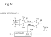
- Fig. 1B is a circuit diagram illustrating a configuration example of the current detector unit 5 in Fig. 1A .
- the current detector unit 5 includes an operational amplifier 21 and a comparator 22. It is noted that Vcc is a power supply voltage.
- the operational amplifier 21 amplifies a voltage corresponding to the inductor current iL detected by the shunt resistor Rs, and outputs an amplified voltage Vamp to the comparator 22.
- the comparator 22 compares the amplified voltage Vamp to be inputted with the reference voltage Vref from the D/A converter 10a in the controller 10, generates a comparison result voltage Vcomp, and outputs the comparison result voltage Vcomp to the controller 10.
- the controller 10 detects the zero current of the inductor current iL based on the comparison result voltage Vcomp, and based on this, controls the drive signal generator circuit 11 to perform switching operation in, for example, the current critical mode to generate the drive signals G1 to G4.
- the polarity of the reference voltage Vref is inverted according to the input voltage Vin ( Fig. 1A ) to the PFC circuit, that is, according to the direction of the inductor current iL.
- the detection delay can be prevented by changing the reference voltage Vref of the comparator 22 according to the delay time.
- deterioration in efficiency can be prevented, the deterioration being caused by the zero point detection delay of the inductor current iL in the PFC circuit of the critical mode.
- Fig. 4A is a circuit diagram illustrating a configuration example of a current detector unit according to a conventional example
- Fig. 4B is a timing chart illustrating an operation of the current detector unit in Fig. 4A
- the reference voltage Vref of the comparator 22 is a constant voltage such as Vcc/2
- a delay time Tdelay occurs as illustrated in Fig. 4B .
- Fig. 4C is a circuit diagram illustrating a configuration example of the current detector unit 5 according to the embodiment
- Fig. 4D is a timing chart illustrating an operation of the current detector unit 5 in Fig. 4C .
- the reference voltage Vref from the D/A converter 10a of the controller 10 is increased according to the delay time. That is, in the PFC circuit in which the input voltage is alternating current (AC), by changing the reference voltage Vref depending on the input voltage Vin, the delay time Tdelay can be reduced as illustrated in Fig. 4D , by comparison with Fig. 4B .
- Fig. 4D In Fig. 4D ,
- Fig. 5 is a graph illustrating an operation of the current detector unit 5 according to an example.
- the delay time Tdelay can be reduced by feeding back and input the first reference voltage Vref derived from the delay time Tdelay to the comparator 22 of the current detector unit 5 by using the current detector unit 5 and the controller 10 in Figs. 1B and 4C .
- Fig. 6 is a block diagram illustrating a configuration example of a power converter apparatus using the PFC circuit according to the embodiment.
- the power converter apparatus includes the AC power supply 1, a PFC circuit 100, a direct current to direct current (DC to DC) converter 101, and a load 102.
- the control target is the PFC circuit
- Vin(t) and Vout are referred to as Vin(t) and Vout, respectively.
- the input voltage Vin(t) is expressed by the following equation.
- Vin t 2 Vin rms ⁇ sin 2 ⁇ LINE t
- Vin(rms) and the line frequency f LINE vary depending on the country or region, and examples thereof are as follows.
- a resistance value of the shunt resistor Rs is denoted as Rs
- a gain of the operational amplifier 21 is denoted as G
- a voltage applied to the operational amplifier 21 and the comparator 22 is denoted as Vcc.
- the controller 10 calculates the first reference voltage Vref for making the delay at the time of detecting the zero value of the inductor current iL substantially zero based on the detected input voltage Vin and output voltage Vout, the preset delay time, the inductance value of the inductor 2, the resistance value of the shunt resistor Rs (in embodiments described later, this is a conversion coefficient when the inductor current iL at the time of current detection is converted into a voltage, and is generally the conversion coefficient), the power supply voltage Vcc, and the gain of the operational amplifier 21, and outputs the first reference voltage Vref to the comparator 22.
- the detection delay of the inductor current can be prevented, and the zero point of the inductor current can be accurately detected as compared with the prior art.
- Fig. 10B is a block diagram illustrating a configuration example of a switching power supply apparatus according to a second embodiment.
- a shunt resistor Rs1 may be inserted between the ground side of switching elements S2 and S4 and a load resistor 4 to detect the zero point of the inductor current iL.
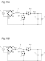
- Fig. 11A is a block diagram illustrating a configuration example of a switching power supply apparatus according to a third embodiment.
- Fig. 11A illustrates an example of a synchronous rectification step-up PFC circuit.
- the switching power supply apparatus is configured by including an AC power supply 1, four bridge-connected diodes D1 to D4, an inductor 2 that is a reactor, switching elements S11 and S12, a shunt resistor Rs2, a smoothing capacitor 3, and a load resistor 4.
- an AC power supply 1 four bridge-connected diodes D1 to D4
- an inductor 2 that is a reactor
- switching elements S11 and S12 switching elements
- a shunt resistor Rs2 a smoothing capacitor 3
- a load resistor 4 Referring to Fig.
- the shunt resistor Rs2 for detecting the zero point of the inductor current iL is preferably inserted between the switching element S12 and the smoothing capacitor 3.
- Fig. 11B is a block diagram illustrating a configuration example of a switching power supply apparatus according to a fourth embodiment.
- a shunt resistor Rs3 for detecting the zero point of the inductor current iL may be inserted between diodes D1 and D4 and an inductor 2.
- Fig. 12 is a circuit diagram illustrating a modified embodiment of the current detector unit 5 in Fig. 1B .
- a controller 10A including a D/A converter 10a, a comparator 22, and a signal processing unit 10b is provided instead of the controller 10.
- the signal processing unit 10b performs signal processing of changing the reference voltage Vref based on the comparison result voltage Vcomp from the comparator 22.
- DSP digital signal processor
- the detection delay of the inductor current can be prevented, and the zero point of the inductor current can be accurately detected as compared with the prior art.
- the loss of the power converter apparatus is reduced, leading to an increase in the density of the power supply apparatus.
- the loss does not increase even when high-frequency driving is performed, and no additional component is required.
- a soft switching function using voltage resonance can be easily implemented.
- the detection delay of the inductor current can be prevented, and the zero point of the inductor current can be accurately detected as compared with the prior art.
- the loss of the power converter apparatus is reduced, and this leads to an increase in the density of the power supply apparatus.
Landscapes
- Engineering & Computer Science (AREA)
- Power Engineering (AREA)
- Rectifiers (AREA)
- Dc-Dc Converters (AREA)
Claims (4)
- Steuerschaltung (20) für eine Leistungswandlungsvorrichtung (101), umfassend eine Leistungsfaktorkorrekturschaltung (100), die einen Induktor (2) beinhaltet und in einem stromkritischen Modus arbeitet, wobei die Steuerschaltung (20) Folgendes umfasst:eine erste Detektorschaltung (5, 21), die konfiguriert ist, um einen Strom des Induktors (2), einen Strom, der dem Strom des Induktors (2) entspricht, oder einen Strom, der den Strom des Induktors (2) beinhaltet, zu erfassen, um eine Spannung, die einem erfassten Strom entspricht, mit einer vorbestimmten Zunahme zu verstärken und um danach eine verstärkte Spannung als erfasste Spannung auszugeben;einen Komparator (22), der konfiguriert ist, um die erfasste Spannung mit einer vorbestimmten zweiten Referenzspannung zu vergleichen und um ein Vergleichsergebnis signal auszugeben;eine zweite Detektorschaltung (12), die konfiguriert ist, um eine Eingangsspannung der Leistungswandlungsvorrichtung (101) zu erfassen; undeine dritte Detektorschaltung (13), die konfiguriert ist, um eine Ausgangsspannung der Leistungswandlungsvorrichtung (101) zu erfassen,wobei die Steuerschaltung (20) konfiguriert ist, um eine erste Referenzspannung zu berechnen, um eine Erfassungsverzögerung zu verhindern und einen Nullpunkt des Induktorstroms genau zu erfassen, indem eine Verzögerung gemacht wird, wenn erfasst wird, dass ein Nullwert des Stroms des Induktors (2) im Wesentlichen Null ist, wobei die erste Referenzspannung auf der erfassten Eingangsspannung, der erfassten Ausgangsspannung, einer voreingestellten Verzögerungszeit, einem Induktivitätswert des Induktors (2), einem Wandlungskoeffizienten, der verwendet wird, wenn der Strom, der durch die erste Detektorschaltung (5, 21) erfasst wird, in eine Spannung umgewandelt wird, einer Leistungsversorgungsspannung und der Zunahme basiert, dadurch gekennzeichnet, dassdie Steuerschaltung (20) konfiguriert ist, um die zweite Referenzspannung unter Berücksichtigung eines negativen Stroms zu berechnen, der durch den Induktor zum sanften Schalten der Leistungswandlungsvorrichtung (101) erforderlich ist, indem die erste Referenzspannung in einer elliptischen Form nur für einen vorbestimmten Zeitraum abgesenkt wird,wobei die Steuerschaltung (20) konfiguriert ist, um den negativen Strom, der für das sanfte Schalten erforderlich ist, basierend auf der Eingangsspannung, die durch die zweite Detektorschaltung (12) erfasst wird, der Ausgangsspannung, die durch die dritte Detektorschaltung (13) erfasst wird, und einer Induktivität des Induktors (2) zu berechnen, undwobei die Steuerschaltung (20) ferner konfiguriert ist, um die zweite Referenzspannung zu berechnen, indem eine Spannung, die dem negativen Strom entspricht, der ersten Referenzspannung hinzugefügt wird, und um die zweite Referenzspannung an den Komparator (22) auszugeben.
- Steuerschaltung (20) für die Leistungswandlungsvorrichtung (101) nach Anspruch 1, wobei die Steuerschaltung (20) einen Digital-Analog(D/A-)Wandler enthält, der D/A-Wandlung an der zweiten Referenzspannung durchführt.
- Leistungswandlungsvorrichtung (101), umfassend die Steuerschaltung (20) für die Leistungswandlungsvorrichtung (101) nach einem der Ansprüche 1 bis 2.
- Leistungswandlungsvorrichtung (101) nach Anspruch 3, wobei die Leistungswandlungsvorrichtung (101) eine Schaltleistungszufuhrvorrichtung oder eine Gleichstrom-Gleichstrom(DC-DC-)Wandlungsvorrichtung ist.
Applications Claiming Priority (1)
| Application Number | Priority Date | Filing Date | Title |
|---|---|---|---|
| PCT/JP2019/031654 WO2021028972A1 (ja) | 2019-08-09 | 2019-08-09 | 電力変換装置の制御回路 |
Publications (3)
| Publication Number | Publication Date |
|---|---|
| EP4012912A1 EP4012912A1 (de) | 2022-06-15 |
| EP4012912A4 EP4012912A4 (de) | 2023-04-12 |
| EP4012912B1 true EP4012912B1 (de) | 2024-05-22 |
Family
ID=74570603
Family Applications (1)
| Application Number | Title | Priority Date | Filing Date |
|---|---|---|---|
| EP19941248.7A Active EP4012912B1 (de) | 2019-08-09 | 2019-08-09 | Steuerschaltung für eine stromwandlungsvorrichtung |
Country Status (5)
| Country | Link |
|---|---|
| US (1) | US12021448B2 (de) |
| EP (1) | EP4012912B1 (de) |
| JP (1) | JP7160208B2 (de) |
| CN (1) | CN114144969B (de) |
| WO (1) | WO2021028972A1 (de) |
Families Citing this family (3)
| Publication number | Priority date | Publication date | Assignee | Title |
|---|---|---|---|---|
| US11764668B2 (en) * | 2018-12-06 | 2023-09-19 | Rohm Co., Ltd. | Control device for controlling an electric power conversion device incorporating a bidirectional inverter |
| CN115085531A (zh) * | 2022-07-05 | 2022-09-20 | 华为数字能源技术有限公司 | 一种图腾柱pfc电路的控制方法、装置和电子设备 |
| CN116015046B (zh) * | 2022-12-30 | 2025-11-18 | 超聚变数字技术有限公司 | 一种开关电源及计算设备 |
Family Cites Families (12)
| Publication number | Priority date | Publication date | Assignee | Title |
|---|---|---|---|---|
| KR101026248B1 (ko) | 2004-09-21 | 2011-03-31 | 페어차일드코리아반도체 주식회사 | 역률 보상 회로 |
| CN101552546B (zh) * | 2008-04-02 | 2011-10-12 | 台达能源技术(上海)有限公司 | 用于临界导通模式的无桥功率因数校正电路及其控制方法 |
| JP5316823B2 (ja) * | 2009-09-11 | 2013-10-16 | 株式会社村田製作所 | Pfcコンバータ |
| US8379420B2 (en) * | 2010-10-13 | 2013-02-19 | Power Integrations, Inc. | Controller with punctuated switching control circuit |
| ITMI20120089A1 (it) * | 2012-01-26 | 2013-07-27 | Dora Spa | Dispositivo di controllo per un alimentatore a commutazione. |
| JP6024201B2 (ja) * | 2012-05-21 | 2016-11-09 | 富士電機株式会社 | スイッチング電源装置 |
| EP2858222A4 (de) * | 2012-05-31 | 2017-03-29 | Nagasaki University, National University Corporation | Vorrichtung zur steuerung einer stromwandlungsschaltung |
| CN203465347U (zh) * | 2013-09-02 | 2014-03-05 | 南京埃科孚电子科技有限公司 | 用于升压型功率因数校正的电感电流过零检测电路 |
| CN103675426B (zh) * | 2013-12-24 | 2017-04-26 | 矽力杰半导体技术(杭州)有限公司 | 电感电流过零检测方法及电路以及带该电路的开关电源 |
| CN104009620A (zh) * | 2014-06-16 | 2014-08-27 | 南京航空航天大学 | 逆变器的控制型软开关技术 |
| US10090757B2 (en) * | 2016-08-19 | 2018-10-02 | Fairchild Semiconductor Corporation | Power factor correction circuit and method |
| US11005361B2 (en) * | 2019-06-19 | 2021-05-11 | Stmicroelectronics S.R.L. | Control circuit and method of a switching power supply |
-
2019
- 2019-08-09 EP EP19941248.7A patent/EP4012912B1/de active Active
- 2019-08-09 WO PCT/JP2019/031654 patent/WO2021028972A1/ja not_active Ceased
- 2019-08-09 US US17/628,692 patent/US12021448B2/en active Active
- 2019-08-09 JP JP2021539708A patent/JP7160208B2/ja active Active
- 2019-08-09 CN CN201980098644.XA patent/CN114144969B/zh active Active
Also Published As
| Publication number | Publication date |
|---|---|
| JP7160208B2 (ja) | 2022-10-25 |
| US20220271650A1 (en) | 2022-08-25 |
| EP4012912A4 (de) | 2023-04-12 |
| JPWO2021028972A1 (de) | 2021-02-18 |
| EP4012912A1 (de) | 2022-06-15 |
| CN114144969A (zh) | 2022-03-04 |
| WO2021028972A1 (ja) | 2021-02-18 |
| CN114144969B (zh) | 2024-11-12 |
| US12021448B2 (en) | 2024-06-25 |
Similar Documents
| Publication | Publication Date | Title |
|---|---|---|
| US12068672B2 (en) | Control circuit for power converter apparatus provided with PFC circuit operating in current-critical mode | |
| US10389233B1 (en) | Switched mode power supply with PFC burst mode control | |
| US8653413B2 (en) | Welding power supply with digital control of duty cycle | |
| JP3994953B2 (ja) | 力率改善回路 | |
| US10367412B2 (en) | Power factor correction circuit and switching power source device using the same | |
| US7317625B2 (en) | Parallel current mode control using a direct duty cycle algorithm with low computational requirements to perform power factor correction | |
| TWI439037B (zh) | 功率因數改善裝置及其控制方法 | |
| EP4012912B1 (de) | Steuerschaltung für eine stromwandlungsvorrichtung | |
| KR20170080518A (ko) | 역률 보상 회로 및 역률 보상 회로의 구동 방법 | |
| US8289738B2 (en) | Switching power supply | |
| JP2011152017A (ja) | スイッチング電源装置 | |
| US20170310209A1 (en) | Multiphase power factor improvement circuit | |
| EP2793382A2 (de) | Stromumwandlungsvorrichtung | |
| JP2008236999A (ja) | 電源装置 | |
| JP2003244953A (ja) | Dc−dcコンバータ | |
| US20220166306A1 (en) | Electrical circuits for power factor correction by measurement and removal of overtones | |
| EP3200336B1 (de) | Stromwandlungsvorrichtung | |
| JP4423994B2 (ja) | 力率改善回路 | |
| JP3495287B2 (ja) | 電力供給装置 | |
| EP3422549A1 (de) | Schaltnetzteilvorrichtung und schaltsteuerkreis | |
| KR20170049173A (ko) | 역률 보상 장치 및 방법 | |
| CN106300954A (zh) | 动态侦测稳压升压功率因数校正控制装置 |
Legal Events
| Date | Code | Title | Description |
|---|---|---|---|
| STAA | Information on the status of an ep patent application or granted ep patent |
Free format text: STATUS: THE INTERNATIONAL PUBLICATION HAS BEEN MADE |
|
| PUAI | Public reference made under article 153(3) epc to a published international application that has entered the european phase |
Free format text: ORIGINAL CODE: 0009012 |
|
| STAA | Information on the status of an ep patent application or granted ep patent |
Free format text: STATUS: REQUEST FOR EXAMINATION WAS MADE |
|
| 17P | Request for examination filed |
Effective date: 20220126 |
|
| AK | Designated contracting states |
Kind code of ref document: A1 Designated state(s): AL AT BE BG CH CY CZ DE DK EE ES FI FR GB GR HR HU IE IS IT LI LT LU LV MC MK MT NL NO PL PT RO RS SE SI SK SM TR |
|
| DAV | Request for validation of the european patent (deleted) | ||
| DAX | Request for extension of the european patent (deleted) | ||
| REG | Reference to a national code |
Ref country code: DE Ref legal event code: R079 Free format text: PREVIOUS MAIN CLASS: H02M0007120000 Ipc: H02M0001000000 Ref country code: DE Ref legal event code: R079 Ref document number: 602019052797 Country of ref document: DE Free format text: PREVIOUS MAIN CLASS: H02M0007120000 Ipc: H02M0001000000 |
|
| A4 | Supplementary search report drawn up and despatched |
Effective date: 20230314 |
|
| RIC1 | Information provided on ipc code assigned before grant |
Ipc: H02M 1/42 20070101ALI20230307BHEP Ipc: H02M 1/00 20060101AFI20230307BHEP |
|
| GRAP | Despatch of communication of intention to grant a patent |
Free format text: ORIGINAL CODE: EPIDOSNIGR1 |
|
| STAA | Information on the status of an ep patent application or granted ep patent |
Free format text: STATUS: GRANT OF PATENT IS INTENDED |
|
| INTG | Intention to grant announced |
Effective date: 20240307 |
|
| GRAS | Grant fee paid |
Free format text: ORIGINAL CODE: EPIDOSNIGR3 |
|
| GRAA | (expected) grant |
Free format text: ORIGINAL CODE: 0009210 |
|
| STAA | Information on the status of an ep patent application or granted ep patent |
Free format text: STATUS: THE PATENT HAS BEEN GRANTED |
|
| AK | Designated contracting states |
Kind code of ref document: B1 Designated state(s): AL AT BE BG CH CY CZ DE DK EE ES FI FR GB GR HR HU IE IS IT LI LT LU LV MC MK MT NL NO PL PT RO RS SE SI SK SM TR |
|
| REG | Reference to a national code |
Ref country code: GB Ref legal event code: FG4D |
|
| REG | Reference to a national code |
Ref country code: CH Ref legal event code: EP |
|
| REG | Reference to a national code |
Ref country code: IE Ref legal event code: FG4D |
|
| REG | Reference to a national code |
Ref country code: DE Ref legal event code: R096 Ref document number: 602019052797 Country of ref document: DE |
|
| REG | Reference to a national code |
Ref country code: LT Ref legal event code: MG9D |
|
| REG | Reference to a national code |
Ref country code: NL Ref legal event code: MP Effective date: 20240522 |
|
| PG25 | Lapsed in a contracting state [announced via postgrant information from national office to epo] |
Ref country code: IS Free format text: LAPSE BECAUSE OF FAILURE TO SUBMIT A TRANSLATION OF THE DESCRIPTION OR TO PAY THE FEE WITHIN THE PRESCRIBED TIME-LIMIT Effective date: 20240922 |
|
| PG25 | Lapsed in a contracting state [announced via postgrant information from national office to epo] |
Ref country code: BG Free format text: LAPSE BECAUSE OF FAILURE TO SUBMIT A TRANSLATION OF THE DESCRIPTION OR TO PAY THE FEE WITHIN THE PRESCRIBED TIME-LIMIT Effective date: 20240522 |
|
| PG25 | Lapsed in a contracting state [announced via postgrant information from national office to epo] |
Ref country code: HR Free format text: LAPSE BECAUSE OF FAILURE TO SUBMIT A TRANSLATION OF THE DESCRIPTION OR TO PAY THE FEE WITHIN THE PRESCRIBED TIME-LIMIT Effective date: 20240522 Ref country code: FI Free format text: LAPSE BECAUSE OF FAILURE TO SUBMIT A TRANSLATION OF THE DESCRIPTION OR TO PAY THE FEE WITHIN THE PRESCRIBED TIME-LIMIT Effective date: 20240522 |
|
| PG25 | Lapsed in a contracting state [announced via postgrant information from national office to epo] |
Ref country code: GR Free format text: LAPSE BECAUSE OF FAILURE TO SUBMIT A TRANSLATION OF THE DESCRIPTION OR TO PAY THE FEE WITHIN THE PRESCRIBED TIME-LIMIT Effective date: 20240823 |
|
| PG25 | Lapsed in a contracting state [announced via postgrant information from national office to epo] |
Ref country code: PT Free format text: LAPSE BECAUSE OF FAILURE TO SUBMIT A TRANSLATION OF THE DESCRIPTION OR TO PAY THE FEE WITHIN THE PRESCRIBED TIME-LIMIT Effective date: 20240923 |
|
| REG | Reference to a national code |
Ref country code: AT Ref legal event code: MK05 Ref document number: 1689574 Country of ref document: AT Kind code of ref document: T Effective date: 20240522 |
|
| PG25 | Lapsed in a contracting state [announced via postgrant information from national office to epo] |
Ref country code: NL Free format text: LAPSE BECAUSE OF FAILURE TO SUBMIT A TRANSLATION OF THE DESCRIPTION OR TO PAY THE FEE WITHIN THE PRESCRIBED TIME-LIMIT Effective date: 20240522 |
|
| PG25 | Lapsed in a contracting state [announced via postgrant information from national office to epo] |
Ref country code: ES Free format text: LAPSE BECAUSE OF FAILURE TO SUBMIT A TRANSLATION OF THE DESCRIPTION OR TO PAY THE FEE WITHIN THE PRESCRIBED TIME-LIMIT Effective date: 20240522 |
|
| PG25 | Lapsed in a contracting state [announced via postgrant information from national office to epo] |
Ref country code: AT Free format text: LAPSE BECAUSE OF FAILURE TO SUBMIT A TRANSLATION OF THE DESCRIPTION OR TO PAY THE FEE WITHIN THE PRESCRIBED TIME-LIMIT Effective date: 20240522 |
|
| PG25 | Lapsed in a contracting state [announced via postgrant information from national office to epo] |
Ref country code: PL Free format text: LAPSE BECAUSE OF FAILURE TO SUBMIT A TRANSLATION OF THE DESCRIPTION OR TO PAY THE FEE WITHIN THE PRESCRIBED TIME-LIMIT Effective date: 20240522 |
|
| PG25 | Lapsed in a contracting state [announced via postgrant information from national office to epo] |
Ref country code: LV Free format text: LAPSE BECAUSE OF FAILURE TO SUBMIT A TRANSLATION OF THE DESCRIPTION OR TO PAY THE FEE WITHIN THE PRESCRIBED TIME-LIMIT Effective date: 20240522 |
|
| PG25 | Lapsed in a contracting state [announced via postgrant information from national office to epo] |
Ref country code: PT Free format text: LAPSE BECAUSE OF FAILURE TO SUBMIT A TRANSLATION OF THE DESCRIPTION OR TO PAY THE FEE WITHIN THE PRESCRIBED TIME-LIMIT Effective date: 20240923 Ref country code: PL Free format text: LAPSE BECAUSE OF FAILURE TO SUBMIT A TRANSLATION OF THE DESCRIPTION OR TO PAY THE FEE WITHIN THE PRESCRIBED TIME-LIMIT Effective date: 20240522 Ref country code: NO Free format text: LAPSE BECAUSE OF FAILURE TO SUBMIT A TRANSLATION OF THE DESCRIPTION OR TO PAY THE FEE WITHIN THE PRESCRIBED TIME-LIMIT Effective date: 20240822 Ref country code: NL Free format text: LAPSE BECAUSE OF FAILURE TO SUBMIT A TRANSLATION OF THE DESCRIPTION OR TO PAY THE FEE WITHIN THE PRESCRIBED TIME-LIMIT Effective date: 20240522 Ref country code: LV Free format text: LAPSE BECAUSE OF FAILURE TO SUBMIT A TRANSLATION OF THE DESCRIPTION OR TO PAY THE FEE WITHIN THE PRESCRIBED TIME-LIMIT Effective date: 20240522 Ref country code: IS Free format text: LAPSE BECAUSE OF FAILURE TO SUBMIT A TRANSLATION OF THE DESCRIPTION OR TO PAY THE FEE WITHIN THE PRESCRIBED TIME-LIMIT Effective date: 20240922 Ref country code: HR Free format text: LAPSE BECAUSE OF FAILURE TO SUBMIT A TRANSLATION OF THE DESCRIPTION OR TO PAY THE FEE WITHIN THE PRESCRIBED TIME-LIMIT Effective date: 20240522 Ref country code: GR Free format text: LAPSE BECAUSE OF FAILURE TO SUBMIT A TRANSLATION OF THE DESCRIPTION OR TO PAY THE FEE WITHIN THE PRESCRIBED TIME-LIMIT Effective date: 20240823 Ref country code: FI Free format text: LAPSE BECAUSE OF FAILURE TO SUBMIT A TRANSLATION OF THE DESCRIPTION OR TO PAY THE FEE WITHIN THE PRESCRIBED TIME-LIMIT Effective date: 20240522 Ref country code: ES Free format text: LAPSE BECAUSE OF FAILURE TO SUBMIT A TRANSLATION OF THE DESCRIPTION OR TO PAY THE FEE WITHIN THE PRESCRIBED TIME-LIMIT Effective date: 20240522 Ref country code: BG Free format text: LAPSE BECAUSE OF FAILURE TO SUBMIT A TRANSLATION OF THE DESCRIPTION OR TO PAY THE FEE WITHIN THE PRESCRIBED TIME-LIMIT Effective date: 20240522 Ref country code: AT Free format text: LAPSE BECAUSE OF FAILURE TO SUBMIT A TRANSLATION OF THE DESCRIPTION OR TO PAY THE FEE WITHIN THE PRESCRIBED TIME-LIMIT Effective date: 20240522 Ref country code: RS Free format text: LAPSE BECAUSE OF FAILURE TO SUBMIT A TRANSLATION OF THE DESCRIPTION OR TO PAY THE FEE WITHIN THE PRESCRIBED TIME-LIMIT Effective date: 20240822 |
|
| PG25 | Lapsed in a contracting state [announced via postgrant information from national office to epo] |
Ref country code: DK Free format text: LAPSE BECAUSE OF FAILURE TO SUBMIT A TRANSLATION OF THE DESCRIPTION OR TO PAY THE FEE WITHIN THE PRESCRIBED TIME-LIMIT Effective date: 20240522 |
|
| PG25 | Lapsed in a contracting state [announced via postgrant information from national office to epo] |
Ref country code: EE Free format text: LAPSE BECAUSE OF FAILURE TO SUBMIT A TRANSLATION OF THE DESCRIPTION OR TO PAY THE FEE WITHIN THE PRESCRIBED TIME-LIMIT Effective date: 20240522 |
|
| PG25 | Lapsed in a contracting state [announced via postgrant information from national office to epo] |
Ref country code: CZ Free format text: LAPSE BECAUSE OF FAILURE TO SUBMIT A TRANSLATION OF THE DESCRIPTION OR TO PAY THE FEE WITHIN THE PRESCRIBED TIME-LIMIT Effective date: 20240522 |
|
| PG25 | Lapsed in a contracting state [announced via postgrant information from national office to epo] |
Ref country code: SK Free format text: LAPSE BECAUSE OF FAILURE TO SUBMIT A TRANSLATION OF THE DESCRIPTION OR TO PAY THE FEE WITHIN THE PRESCRIBED TIME-LIMIT Effective date: 20240522 Ref country code: RO Free format text: LAPSE BECAUSE OF FAILURE TO SUBMIT A TRANSLATION OF THE DESCRIPTION OR TO PAY THE FEE WITHIN THE PRESCRIBED TIME-LIMIT Effective date: 20240522 |
|
| PG25 | Lapsed in a contracting state [announced via postgrant information from national office to epo] |
Ref country code: SM Free format text: LAPSE BECAUSE OF FAILURE TO SUBMIT A TRANSLATION OF THE DESCRIPTION OR TO PAY THE FEE WITHIN THE PRESCRIBED TIME-LIMIT Effective date: 20240522 |
|
| PG25 | Lapsed in a contracting state [announced via postgrant information from national office to epo] |
Ref country code: SM Free format text: LAPSE BECAUSE OF FAILURE TO SUBMIT A TRANSLATION OF THE DESCRIPTION OR TO PAY THE FEE WITHIN THE PRESCRIBED TIME-LIMIT Effective date: 20240522 Ref country code: SK Free format text: LAPSE BECAUSE OF FAILURE TO SUBMIT A TRANSLATION OF THE DESCRIPTION OR TO PAY THE FEE WITHIN THE PRESCRIBED TIME-LIMIT Effective date: 20240522 Ref country code: RO Free format text: LAPSE BECAUSE OF FAILURE TO SUBMIT A TRANSLATION OF THE DESCRIPTION OR TO PAY THE FEE WITHIN THE PRESCRIBED TIME-LIMIT Effective date: 20240522 Ref country code: EE Free format text: LAPSE BECAUSE OF FAILURE TO SUBMIT A TRANSLATION OF THE DESCRIPTION OR TO PAY THE FEE WITHIN THE PRESCRIBED TIME-LIMIT Effective date: 20240522 Ref country code: DK Free format text: LAPSE BECAUSE OF FAILURE TO SUBMIT A TRANSLATION OF THE DESCRIPTION OR TO PAY THE FEE WITHIN THE PRESCRIBED TIME-LIMIT Effective date: 20240522 Ref country code: CZ Free format text: LAPSE BECAUSE OF FAILURE TO SUBMIT A TRANSLATION OF THE DESCRIPTION OR TO PAY THE FEE WITHIN THE PRESCRIBED TIME-LIMIT Effective date: 20240522 |
|
| PG25 | Lapsed in a contracting state [announced via postgrant information from national office to epo] |
Ref country code: IT Free format text: LAPSE BECAUSE OF FAILURE TO SUBMIT A TRANSLATION OF THE DESCRIPTION OR TO PAY THE FEE WITHIN THE PRESCRIBED TIME-LIMIT Effective date: 20240522 |
|
| REG | Reference to a national code |
Ref country code: DE Ref legal event code: R097 Ref document number: 602019052797 Country of ref document: DE |
|
| PLBE | No opposition filed within time limit |
Free format text: ORIGINAL CODE: 0009261 |
|
| STAA | Information on the status of an ep patent application or granted ep patent |
Free format text: STATUS: NO OPPOSITION FILED WITHIN TIME LIMIT |
|
| REG | Reference to a national code |
Ref country code: CH Ref legal event code: PL |
|
| PG25 | Lapsed in a contracting state [announced via postgrant information from national office to epo] |
Ref country code: LU Free format text: LAPSE BECAUSE OF NON-PAYMENT OF DUE FEES Effective date: 20240809 |
|
| GBPC | Gb: european patent ceased through non-payment of renewal fee |
Effective date: 20240822 |
|
| PG25 | Lapsed in a contracting state [announced via postgrant information from national office to epo] |
Ref country code: SI Free format text: LAPSE BECAUSE OF FAILURE TO SUBMIT A TRANSLATION OF THE DESCRIPTION OR TO PAY THE FEE WITHIN THE PRESCRIBED TIME-LIMIT Effective date: 20240522 Ref country code: MC Free format text: LAPSE BECAUSE OF FAILURE TO SUBMIT A TRANSLATION OF THE DESCRIPTION OR TO PAY THE FEE WITHIN THE PRESCRIBED TIME-LIMIT Effective date: 20240522 Ref country code: CH Free format text: LAPSE BECAUSE OF NON-PAYMENT OF DUE FEES Effective date: 20240831 |
|
| 26N | No opposition filed |
Effective date: 20250225 |
|
| REG | Reference to a national code |
Ref country code: BE Ref legal event code: MM Effective date: 20240831 |
|
| PG25 | Lapsed in a contracting state [announced via postgrant information from national office to epo] |
Ref country code: GB Free format text: LAPSE BECAUSE OF NON-PAYMENT OF DUE FEES Effective date: 20240822 |
|
| PG25 | Lapsed in a contracting state [announced via postgrant information from national office to epo] |
Ref country code: BE Free format text: LAPSE BECAUSE OF NON-PAYMENT OF DUE FEES Effective date: 20240831 |
|
| PG25 | Lapsed in a contracting state [announced via postgrant information from national office to epo] |
Ref country code: FR Free format text: LAPSE BECAUSE OF NON-PAYMENT OF DUE FEES Effective date: 20240831 |
|
| PG25 | Lapsed in a contracting state [announced via postgrant information from national office to epo] |
Ref country code: IE Free format text: LAPSE BECAUSE OF NON-PAYMENT OF DUE FEES Effective date: 20240809 |
|
| PG25 | Lapsed in a contracting state [announced via postgrant information from national office to epo] |
Ref country code: SE Free format text: LAPSE BECAUSE OF FAILURE TO SUBMIT A TRANSLATION OF THE DESCRIPTION OR TO PAY THE FEE WITHIN THE PRESCRIBED TIME-LIMIT Effective date: 20240522 |
|
| PGFP | Annual fee paid to national office [announced via postgrant information from national office to epo] |
Ref country code: DE Payment date: 20250806 Year of fee payment: 7 |
|
| PG25 | Lapsed in a contracting state [announced via postgrant information from national office to epo] |
Ref country code: CY Free format text: LAPSE BECAUSE OF FAILURE TO SUBMIT A TRANSLATION OF THE DESCRIPTION OR TO PAY THE FEE WITHIN THE PRESCRIBED TIME-LIMIT; INVALID AB INITIO Effective date: 20190809 |