EP4006984B1 - Appareil d'affichage et module d'affichage - Google Patents
Appareil d'affichage et module d'affichage Download PDFInfo
- Publication number
- EP4006984B1 EP4006984B1 EP19933240.4A EP19933240A EP4006984B1 EP 4006984 B1 EP4006984 B1 EP 4006984B1 EP 19933240 A EP19933240 A EP 19933240A EP 4006984 B1 EP4006984 B1 EP 4006984B1
- Authority
- EP
- European Patent Office
- Prior art keywords
- panel part
- antenna
- display module
- wave
- absorbing layer
- Prior art date
- Legal status (The legal status is an assumption and is not a legal conclusion. Google has not performed a legal analysis and makes no representation as to the accuracy of the status listed.)
- Active
Links
- 239000010410 layer Substances 0.000 claims description 164
- 239000012790 adhesive layer Substances 0.000 claims description 18
- 238000000034 method Methods 0.000 description 28
- RYGMFSIKBFXOCR-UHFFFAOYSA-N Copper Chemical compound [Cu] RYGMFSIKBFXOCR-UHFFFAOYSA-N 0.000 description 17
- 238000010586 diagram Methods 0.000 description 16
- 229920002120 photoresistant polymer Polymers 0.000 description 13
- 239000000463 material Substances 0.000 description 12
- 229910052802 copper Inorganic materials 0.000 description 10
- 239000010949 copper Substances 0.000 description 10
- 229910052751 metal Inorganic materials 0.000 description 10
- 239000002184 metal Substances 0.000 description 10
- 239000011889 copper foil Substances 0.000 description 7
- 238000004519 manufacturing process Methods 0.000 description 7
- 229910052782 aluminium Inorganic materials 0.000 description 6
- XAGFODPZIPBFFR-UHFFFAOYSA-N aluminium Chemical compound [Al] XAGFODPZIPBFFR-UHFFFAOYSA-N 0.000 description 6
- 239000004744 fabric Substances 0.000 description 6
- 238000000059 patterning Methods 0.000 description 6
- VYPSYNLAJGMNEJ-UHFFFAOYSA-N Silicium dioxide Chemical compound O=[Si]=O VYPSYNLAJGMNEJ-UHFFFAOYSA-N 0.000 description 5
- 230000003247 decreasing effect Effects 0.000 description 5
- XEEYBQQBJWHFJM-UHFFFAOYSA-N Iron Chemical compound [Fe] XEEYBQQBJWHFJM-UHFFFAOYSA-N 0.000 description 4
- 239000000853 adhesive Substances 0.000 description 4
- 230000001070 adhesive effect Effects 0.000 description 4
- 239000000956 alloy Substances 0.000 description 4
- 239000011248 coating agent Substances 0.000 description 4
- 238000000576 coating method Methods 0.000 description 4
- 239000011888 foil Substances 0.000 description 4
- 229910000859 α-Fe Inorganic materials 0.000 description 4
- 238000005530 etching Methods 0.000 description 3
- 239000006260 foam Substances 0.000 description 3
- 229910052814 silicon oxide Inorganic materials 0.000 description 3
- 238000004544 sputter deposition Methods 0.000 description 3
- 239000000758 substrate Substances 0.000 description 3
- OKTJSMMVPCPJKN-UHFFFAOYSA-N Carbon Chemical compound [C] OKTJSMMVPCPJKN-UHFFFAOYSA-N 0.000 description 2
- ZOKXTWBITQBERF-UHFFFAOYSA-N Molybdenum Chemical compound [Mo] ZOKXTWBITQBERF-UHFFFAOYSA-N 0.000 description 2
- 230000005540 biological transmission Effects 0.000 description 2
- 229910052681 coesite Inorganic materials 0.000 description 2
- 229910052906 cristobalite Inorganic materials 0.000 description 2
- 238000000151 deposition Methods 0.000 description 2
- 230000008021 deposition Effects 0.000 description 2
- 238000005516 engineering process Methods 0.000 description 2
- 229910021389 graphene Inorganic materials 0.000 description 2
- 230000002452 interceptive effect Effects 0.000 description 2
- 229910052742 iron Inorganic materials 0.000 description 2
- 239000007769 metal material Substances 0.000 description 2
- 229910052750 molybdenum Inorganic materials 0.000 description 2
- 239000011733 molybdenum Substances 0.000 description 2
- 239000002086 nanomaterial Substances 0.000 description 2
- 230000003287 optical effect Effects 0.000 description 2
- 229920000642 polymer Polymers 0.000 description 2
- HBMJWWWQQXIZIP-UHFFFAOYSA-N silicon carbide Chemical compound [Si+]#[C-] HBMJWWWQQXIZIP-UHFFFAOYSA-N 0.000 description 2
- 229910010271 silicon carbide Inorganic materials 0.000 description 2
- 239000000377 silicon dioxide Substances 0.000 description 2
- 229910052682 stishovite Inorganic materials 0.000 description 2
- 229910052905 tridymite Inorganic materials 0.000 description 2
- 229910000838 Al alloy Inorganic materials 0.000 description 1
- 229910004205 SiNX Inorganic materials 0.000 description 1
- PNEYBMLMFCGWSK-UHFFFAOYSA-N aluminium oxide Inorganic materials [O-2].[O-2].[O-2].[Al+3].[Al+3] PNEYBMLMFCGWSK-UHFFFAOYSA-N 0.000 description 1
- 229910052593 corundum Inorganic materials 0.000 description 1
- 230000001419 dependent effect Effects 0.000 description 1
- 238000005192 partition Methods 0.000 description 1
- 238000002360 preparation method Methods 0.000 description 1
- 239000002096 quantum dot Substances 0.000 description 1
- 230000000717 retained effect Effects 0.000 description 1
- 238000002207 thermal evaporation Methods 0.000 description 1
- 229910001845 yogo sapphire Inorganic materials 0.000 description 1
Images

Classifications
-
- H—ELECTRICITY
- H01—ELECTRIC ELEMENTS
- H01Q—ANTENNAS, i.e. RADIO AERIALS
- H01Q1/00—Details of, or arrangements associated with, antennas
- H01Q1/12—Supports; Mounting means
- H01Q1/22—Supports; Mounting means by structural association with other equipment or articles
- H01Q1/24—Supports; Mounting means by structural association with other equipment or articles with receiving set
- H01Q1/241—Supports; Mounting means by structural association with other equipment or articles with receiving set used in mobile communications, e.g. GSM
- H01Q1/242—Supports; Mounting means by structural association with other equipment or articles with receiving set used in mobile communications, e.g. GSM specially adapted for hand-held use
- H01Q1/243—Supports; Mounting means by structural association with other equipment or articles with receiving set used in mobile communications, e.g. GSM specially adapted for hand-held use with built-in antennas
-
- G—PHYSICS
- G09—EDUCATION; CRYPTOGRAPHY; DISPLAY; ADVERTISING; SEALS
- G09G—ARRANGEMENTS OR CIRCUITS FOR CONTROL OF INDICATING DEVICES USING STATIC MEANS TO PRESENT VARIABLE INFORMATION
- G09G3/00—Control arrangements or circuits, of interest only in connection with visual indicators other than cathode-ray tubes
- G09G3/20—Control arrangements or circuits, of interest only in connection with visual indicators other than cathode-ray tubes for presentation of an assembly of a number of characters, e.g. a page, by composing the assembly by combination of individual elements arranged in a matrix no fixed position being assigned to or needed to be assigned to the individual characters or partial characters
- G09G3/22—Control arrangements or circuits, of interest only in connection with visual indicators other than cathode-ray tubes for presentation of an assembly of a number of characters, e.g. a page, by composing the assembly by combination of individual elements arranged in a matrix no fixed position being assigned to or needed to be assigned to the individual characters or partial characters using controlled light sources
- G09G3/30—Control arrangements or circuits, of interest only in connection with visual indicators other than cathode-ray tubes for presentation of an assembly of a number of characters, e.g. a page, by composing the assembly by combination of individual elements arranged in a matrix no fixed position being assigned to or needed to be assigned to the individual characters or partial characters using controlled light sources using electroluminescent panels
- G09G3/32—Control arrangements or circuits, of interest only in connection with visual indicators other than cathode-ray tubes for presentation of an assembly of a number of characters, e.g. a page, by composing the assembly by combination of individual elements arranged in a matrix no fixed position being assigned to or needed to be assigned to the individual characters or partial characters using controlled light sources using electroluminescent panels semiconductive, e.g. using light-emitting diodes [LED]
- G09G3/3208—Control arrangements or circuits, of interest only in connection with visual indicators other than cathode-ray tubes for presentation of an assembly of a number of characters, e.g. a page, by composing the assembly by combination of individual elements arranged in a matrix no fixed position being assigned to or needed to be assigned to the individual characters or partial characters using controlled light sources using electroluminescent panels semiconductive, e.g. using light-emitting diodes [LED] organic, e.g. using organic light-emitting diodes [OLED]
-
- G—PHYSICS
- G06—COMPUTING; CALCULATING OR COUNTING
- G06F—ELECTRIC DIGITAL DATA PROCESSING
- G06F1/00—Details not covered by groups G06F3/00 - G06F13/00 and G06F21/00
- G06F1/16—Constructional details or arrangements
- G06F1/1613—Constructional details or arrangements for portable computers
- G06F1/1626—Constructional details or arrangements for portable computers with a single-body enclosure integrating a flat display, e.g. Personal Digital Assistants [PDAs]
-
- G—PHYSICS
- G06—COMPUTING; CALCULATING OR COUNTING
- G06F—ELECTRIC DIGITAL DATA PROCESSING
- G06F1/00—Details not covered by groups G06F3/00 - G06F13/00 and G06F21/00
- G06F1/16—Constructional details or arrangements
- G06F1/1613—Constructional details or arrangements for portable computers
- G06F1/1633—Constructional details or arrangements of portable computers not specific to the type of enclosures covered by groups G06F1/1615 - G06F1/1626
- G06F1/1637—Details related to the display arrangement, including those related to the mounting of the display in the housing
-
- G—PHYSICS
- G06—COMPUTING; CALCULATING OR COUNTING
- G06F—ELECTRIC DIGITAL DATA PROCESSING
- G06F1/00—Details not covered by groups G06F3/00 - G06F13/00 and G06F21/00
- G06F1/16—Constructional details or arrangements
- G06F1/1613—Constructional details or arrangements for portable computers
- G06F1/1633—Constructional details or arrangements of portable computers not specific to the type of enclosures covered by groups G06F1/1615 - G06F1/1626
- G06F1/1656—Details related to functional adaptations of the enclosure, e.g. to provide protection against EMI, shock, water, or to host detachable peripherals like a mouse or removable expansions units like PCMCIA cards, or to provide access to internal components for maintenance or to removable storage supports like CDs or DVDs, or to mechanically mount accessories
- G06F1/1658—Details related to functional adaptations of the enclosure, e.g. to provide protection against EMI, shock, water, or to host detachable peripherals like a mouse or removable expansions units like PCMCIA cards, or to provide access to internal components for maintenance or to removable storage supports like CDs or DVDs, or to mechanically mount accessories related to the mounting of internal components, e.g. disc drive or any other functional module
-
- G—PHYSICS
- G06—COMPUTING; CALCULATING OR COUNTING
- G06F—ELECTRIC DIGITAL DATA PROCESSING
- G06F1/00—Details not covered by groups G06F3/00 - G06F13/00 and G06F21/00
- G06F1/16—Constructional details or arrangements
- G06F1/1613—Constructional details or arrangements for portable computers
- G06F1/1633—Constructional details or arrangements of portable computers not specific to the type of enclosures covered by groups G06F1/1615 - G06F1/1626
- G06F1/1684—Constructional details or arrangements related to integrated I/O peripherals not covered by groups G06F1/1635 - G06F1/1675
- G06F1/1698—Constructional details or arrangements related to integrated I/O peripherals not covered by groups G06F1/1635 - G06F1/1675 the I/O peripheral being a sending/receiving arrangement to establish a cordless communication link, e.g. radio or infrared link, integrated cellular phone
-
- G—PHYSICS
- G06—COMPUTING; CALCULATING OR COUNTING
- G06F—ELECTRIC DIGITAL DATA PROCESSING
- G06F1/00—Details not covered by groups G06F3/00 - G06F13/00 and G06F21/00
- G06F1/16—Constructional details or arrangements
- G06F1/20—Cooling means
- G06F1/203—Cooling means for portable computers, e.g. for laptops
-
- G—PHYSICS
- G09—EDUCATION; CRYPTOGRAPHY; DISPLAY; ADVERTISING; SEALS
- G09G—ARRANGEMENTS OR CIRCUITS FOR CONTROL OF INDICATING DEVICES USING STATIC MEANS TO PRESENT VARIABLE INFORMATION
- G09G3/00—Control arrangements or circuits, of interest only in connection with visual indicators other than cathode-ray tubes
- G09G3/20—Control arrangements or circuits, of interest only in connection with visual indicators other than cathode-ray tubes for presentation of an assembly of a number of characters, e.g. a page, by composing the assembly by combination of individual elements arranged in a matrix no fixed position being assigned to or needed to be assigned to the individual characters or partial characters
-
- H—ELECTRICITY
- H01—ELECTRIC ELEMENTS
- H01L—SEMICONDUCTOR DEVICES NOT COVERED BY CLASS H10
- H01L27/00—Devices consisting of a plurality of semiconductor or other solid-state components formed in or on a common substrate
- H01L27/02—Devices consisting of a plurality of semiconductor or other solid-state components formed in or on a common substrate including semiconductor components specially adapted for rectifying, oscillating, amplifying or switching and having potential barriers; including integrated passive circuit elements having potential barriers
- H01L27/12—Devices consisting of a plurality of semiconductor or other solid-state components formed in or on a common substrate including semiconductor components specially adapted for rectifying, oscillating, amplifying or switching and having potential barriers; including integrated passive circuit elements having potential barriers the substrate being other than a semiconductor body, e.g. an insulating body
-
- G—PHYSICS
- G09—EDUCATION; CRYPTOGRAPHY; DISPLAY; ADVERTISING; SEALS
- G09G—ARRANGEMENTS OR CIRCUITS FOR CONTROL OF INDICATING DEVICES USING STATIC MEANS TO PRESENT VARIABLE INFORMATION
- G09G2300/00—Aspects of the constitution of display devices
- G09G2300/04—Structural and physical details of display devices
- G09G2300/0421—Structural details of the set of electrodes
- G09G2300/0426—Layout of electrodes and connections
-
- G—PHYSICS
- G09—EDUCATION; CRYPTOGRAPHY; DISPLAY; ADVERTISING; SEALS
- G09G—ARRANGEMENTS OR CIRCUITS FOR CONTROL OF INDICATING DEVICES USING STATIC MEANS TO PRESENT VARIABLE INFORMATION
- G09G2310/00—Command of the display device
- G09G2310/02—Addressing, scanning or driving the display screen or processing steps related thereto
- G09G2310/0264—Details of driving circuits
- G09G2310/0297—Special arrangements with multiplexing or demultiplexing of display data in the drivers for data electrodes, in a pre-processing circuitry delivering display data to said drivers or in the matrix panel, e.g. multiplexing plural data signals to one D/A converter or demultiplexing the D/A converter output to multiple columns
-
- G—PHYSICS
- G09—EDUCATION; CRYPTOGRAPHY; DISPLAY; ADVERTISING; SEALS
- G09G—ARRANGEMENTS OR CIRCUITS FOR CONTROL OF INDICATING DEVICES USING STATIC MEANS TO PRESENT VARIABLE INFORMATION
- G09G2330/00—Aspects of power supply; Aspects of display protection and defect management
- G09G2330/04—Display protection
- G09G2330/045—Protection against panel overheating
-
- G—PHYSICS
- G09—EDUCATION; CRYPTOGRAPHY; DISPLAY; ADVERTISING; SEALS
- G09G—ARRANGEMENTS OR CIRCUITS FOR CONTROL OF INDICATING DEVICES USING STATIC MEANS TO PRESENT VARIABLE INFORMATION
- G09G2330/00—Aspects of power supply; Aspects of display protection and defect management
- G09G2330/06—Handling electromagnetic interferences [EMI], covering emitted as well as received electromagnetic radiation
Definitions
- the present disclosure relates to the field of display technologies, and in particular, to a display device and a display module.
- a full-screen display device has a compact structure, a high screen-to-body ratio and a narrow frame.
- a display integrated circuit (IC) of a display panel is connected with a signal line in a display panel with a multiplexer (MUX) so as to reduce an area of a wiring region of the display panel and thus achieve the high screen-to-body ratio and frame narrowing of the display device.
- IC display integrated circuit
- MUX multiplexer
- KR 2017 0119623 A describes a display that includes at least one pixel and at least a part of the area is transparent, a screen is disposed in a certain area below the display, irradiated from a pixel disposed on the display and directed by an object approaching the display.
- WO 2019/112314 A1 describes an electronic apparatus.
- a display module is provided, in accordance with appended independent claim 1.
- a display device is provided in accordance with appended claim 2.
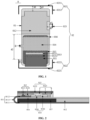
- FIG. 1 is a front view structural schematic diagram of a display device 0 according to an embodiment of the present disclosure.
- the display device 0 includes a display module 01 and a middle frame antenna 02 located around the display module 01.
- the display module 01 includes a display panel 011, a wave-absorbing layer 012, a driving circuit 013 and a flexible circuit board 014.
- FIG. 2 is a sectional view structural schematic diagram of the display module 01 according to the embodiment of the present disclosure.
- the display panel 011 includes a first panel part 0111, a second panel part 0112, and a bent panel part 0113 connecting the first panel part 0111 and the second panel part 0112.
- the second panel part 0112 is located on a back surface of the first panel part 0111.
- the wave-absorbing layer 012 is located between the first panel part 0111 and the second panel part 0112 and the minimum distance between the boundary of the wave-absorbing layer 012 and the middle frame antenna 02 is greater than or equal to 8 millimeters.
- the driving circuit 013 is located on a side, away from the first panel part 0111, of the second panel part 0112 and electrically connected with the display panel 011.
- the flexible circuit board 014 is located on the back surface of the first panel part 0111 and electrically connected with an end, away from the bent panel part 0113, of the second panel part 0112. As shown in FIG. 2 , an orthographic projection of the driving circuit 013 on the first panel part 0111, an orthographic projection of the flexible circuit board 014 on the first panel part 0111, and an orthographic projection of the wave-absorbing layer 012 on the first panel part 0111 do not overlap.
- first panel part 0111 and the second panel part 0112 may be parallel to each other or the first panel part 0111 is substantially parallel to the second panel part 0112.
- an angle between the first panel part 0111 and the second panel part 0112 is less than 5 degrees.
- the back surface of the first panel part 0111 may be a surface, close to the second panel part 0112, of the first panel part 0111.
- the minimum distance between the boundary of the wave-absorbing layer 012 and the middle frame antenna 02 is greater than or equal to 8 millimeters.
- the minimum distance between the boundary of the wave-absorbing layer 012 and the middle frame antenna 02 is greater than or equal to 10 millimeters.
- the wave-absorbing layer 012 may be made of one or more of ferrite, magnetic iron nanomaterial, silicon carbide and a graphene polymer. It is well understood by a person skilled in the art that the driving circuit 013 generates an interference signal in an operation process and the interference signal will be transmitted along the display panel 011.
- the wave-absorbing layer 012 may convert the interference signal into heat and then dissipate the same so as to absorb the interference signal. Therefore, the situation that the interference signal is transmitted to the middle frame antenna 02 to affect a signal of the middle frame antenna 02 is avoided.
- FIG. 3 shows a diagram illustrating the transmission of the interference signal along the display panel 011 according to the embodiment of the present disclosure.
- the driving circuit 013 includes a multiplexer (MUX) 0131 and a display integrated circuit (IC) 0132. Both the MUX 0131 and display IC 0132 are located on a surface, away from the first panel part 0111, of the second panel part 0112.
- the display IC 0132 is electrically connected with the display panel 011 through the MUX 0131.
- the MUX 0131 may be a 1: n MUX. That is, each input port in the MUX 0131 corresponds to n output ports, and n is an integer greater than 1.
- Each input port of the MUX 0131 may be connected with one output port of the display IC 0132.
- Each output port of the MUX 0131 may be connected with a signal line (such as a data line) of the display panel 011.
- a signal line such as a data line
- the use of the MUX enables the display IC to be connected with more signal wiring.
- the use of the MUX may achieve a smaller area of a fan-out region (i.e., a wiring region) of the display module.
- FIG. 4 shows a diagram illustrating the connection of the MUX 0131 and the display IC 0132 according to the embodiment of the present disclosure.
- the description is given with an example that the display IC 0132 is connected with two MUXs 0131 (including a MUX 0131a and a MUX 0131b) and each MUX is a 1: 2 MUX.
- two output ports (not labeled in FIG. 4 ) of the display IC 0132 are connected with input ports (not labeled in FIG. 4 ) of the two MUXs in a one-to-one correspondence.
- Each input port of the MUX 0131a corresponds to two output ports.
- the two output ports of the MUX 0131a are connected with signal wiring D1 and signal wiring D2 in a one-to-one correspondence.
- Each input port of the MUX 0131b corresponds to two output ports.
- the two output ports of the MUX 0131b are connected with signal wiring D3 and signal wiring D4 in a one-to-one correspondence.
- Each output port of the MUX has a switch unit (not labeled in FIG. 4 ) and the MUX achieves the data routing through the switch unit.
- FIG. 5 shows a routing diagram of the MUX 0131a shown in FIG. 4 .
- the MUX 0131a When the switch unit S1 is switched on and the switch unit S2 is switched off, the MUX 0131a causes the display IC 0132 to be electrically connected with the signal wiring D1, and the display IC 0132 to be disconnected from the signal wiring D2. Thus, the MUX 0131a selects the signal wiring D1 as a route for the display IC 0132.
- FIG. 6 shows a routing diagram of another MUX 0131a shown in FIG. 4 .
- the MUX 0131a causes the display IC 0132 to be electrically connected with the signal wiring D2, and the display IC 0132 to be disconnected from the signal wiring D1.
- the MUX 0131a selects the signal wiring D2 as a route for the display IC 0132. It is well understood by a person skilled in the art that in the embodiment of the present disclosure, the description is given by taking the MUX 0131a, which performs routing, as an example. The routing principles of the MUX 0131b and other MUXs in the display module are similar to that of the MUX 0131a and thus will not be repeated in the embodiment of the present disclosure.
- the display module 01 further includes a shielding film 015 located on a side, away from the first panel part 0111 of the driving circuit 013.
- An orthographic projection of the shielding film 015 on the first panel part 0111 covers the orthographic projection of the driving circuit 013 on the first panel part 0111 and the orthographic projection of the flexible circuit board 014 on the first panel part 0111, and the orthographic projection of the shielding film 015 on the first panel part 0111 does not overlap with the orthographic projection of the wave-absorbing layer 012 on the first panel part 0111.
- the shielding film 015 may shield the interference signal generated by the driving circuit 013, thereby avoiding the situation that the interference signal is transmitted to the middle frame antenna 02 to affect the signal of the middle frame antenna 02.
- the shielding film 015 may include an adhesive layer 0151 and a shielding layer 0152 which are stacked.
- the shielding film 015 is adhered to the side, away from the first panel part 0111, of the driving circuit 013 through the adhesive layer 0151.
- the adhesive layer 0151 may include a first conductive portion a, a second conductive portion b and an insulating portion c except the first conductive portion a and the second conductive portion b.
- the first conductive portion a is electrically connected with the second conductive portion b (not shown in FIG. 2 ).
- the shielding layer 0152 may include one or more of a conductive fabric, copper foil and aluminum foil.
- the shielding layer 0152 is a conductive fabric.
- the display module 01 further includes a heat-dissipating film 016 located between the first panel part 0111 and the second panel part 0112, and between the first panel part 0111 and the flexible circuit board 014 and part of the heat-dissipating film 016 is in contact with the second panel part 0112 and the flexible circuit board 014.
- the heat-dissipating film 016 may be made of metal.
- the heat-dissipating film 016 is copper foil.
- the driving circuit 013 and the flexible circuit board 014 likely generate heat.
- the heat generated by the driving circuit 013 may be transferred to the heat-dissipating film 016 through the second panel part 0112 and then is dissipated from the display module 01 by the heat-dissipating film 016.
- the heat generated by the flexible circuit board 014 may be directly transferred to the heat-dissipating film 016 and then is dissipated from the display module 01 by the heat-dissipating film 016. Therefore, the heat-dissipating film 016 may effectively dissipate the heat generated by the display module 01.
- the display module 01 further includes a buffer layer 017 located between the heat-dissipating film 016 and the first panel part 0111 and distributed on the same layer as the wave-absorbing layer 012.
- the buffer layer 017 may be a foam layer.
- the buffer layer 017 may buffer the heat-dissipating film 016 and other structures to reduce stress of the heat-dissipating film 016 and other structures.
- the flexible circuit board 014 may have two ends. One end (not labeled in both FIGS. 1 and 2 ) of the flexible circuit board 014 is electrically connected with an end, away from the bent panel part 0113, of the second panel part 0112 and the other end E (as shown in FIG. 1 , but not shown in FIG. 2 ) thereof is configured to be electrically connected with a client mainboard (not shown in both FIGS. 1 and 2 ).
- the flexible circuit board 014 includes a conductive layer 0141 and an insulating layer 0142 which are stacked.
- the conductive layer 0141 may be a copper layer.
- the insulating layer 0142 has an opening (not labeled in both FIGS.
- the adhesive layer 0151 includes the first conductive portion a, the second conductive portion b and the insulating portion c except the first conductive portion a and the second conductive portion b.
- the first conductive portion a is electrically connected with the second conductive portion b (not shown in FIG. 2 ).
- the shielding film 015 is electrically connected with the flexible circuit board 014 through the first conductive portion a and electrically connected with the heat-dissipating film 016 through the second conductive portion b, and the shielding film 015 is grounded.
- the orthographic projection of the first conductive portion a on the first panel part 0111 may cover the orthographic projection of the opening of the flexible circuit board 014 on the first panel part 0111. As such, it is convenient for a sufficient contact between the first conductive portion a and the conductive layer 0141and thus ensuring the effective connection of the shielding film 016 with the flexible circuit board 014.
- the middle frame antenna 02 may be configured to emit and receive an electromagnetic wave signal and may have different forms.
- the description is given by taking the middle frame antenna 02 of three different forms as an example.
- the middle frame antenna 02 includes an upper antenna 021, a lower antenna 022 and a side antenna 023.
- the upper antenna 021 and the lower antenna 022 may adopt the same structure.
- the upper antenna 021 may be of a U-shaped structure.
- the upper antenna 021 includes a bottom edge 0211 and two side edges 0212 located at two ends of the bottom edge 0211.
- the upper antenna 021 is located at the top of the display module 01.
- the bottom edge 0211 of the upper antenna 021 extends along a top edge (not labeled in FIG. 1 ) of the display module 01 and the two side edges 0212 of the upper antenna 021 extend along two side edges (not labeled in FIG. 1 ) of the display module 01.
- the lower antenna 022 may be of a U-shaped structure.
- the lower antenna 022 includes a bottom edge 0221 and two side edges 0222 located at two ends of the bottom edge 0221.
- the lower antenna 022 is located at the bottom of the display module 01.
- a bottom edge 0221 of the lower antenna 022 extends along a bottom edge (not labeled in FIG. 1 ) of the display module 01 and two side edges 0222 of the lower antenna 022 extend along two side edges (not labeled in FIG .1 ) of the display module 01.
- the side antenna 023 may be of a linear structure.
- the side antenna 023 extends along a side edge of the display module 01 and is located between the upper antenna 021 and the lower antenna 022.
- a minimum distance d1 between the boundary of the wave-absorbing layer 012 and the upper antenna 021 and a minimum distance d3 between the boundary of the wave-absorbing layer 012 and the side antenna 023 may be greater than or equal to 8 millimeters.
- the minimum distance d1 between the boundary of the wave-absorbing layer 012 and the upper antenna 021 is equal to the minimum distance d3 between the boundary of the wave-absorbing layer 012 and the side antenna 023.
- a minimum distance d2 between the boundary of the wave-absorbing layer 012 and the lower antenna 022 may be greater than 8 millimeters.
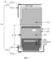
- the middle frame antenna 02 may include an upper antenna 021 and a lower antenna 022.
- the upper antenna 021 may be of an L-shaped structure and includes a first edge 0211 and a second edge 0212.
- the first edge 0211 has a length greater than that of the second edge 0212.
- the upper antenna 021 is located at the top of the display module 01, the first edge 0211 extends along a top edge (not labeled in FIG. 7 ) of the display module 01 and the second edge 0212 extends along one side edge (not labeled in FIG. 7 ) of the display module 01.
- the lower antenna 022 may be of a U-shaped structure.
- the lower antenna 022 includes a bottom edge 0221 and two side edges 0222 located at two ends of the bottom edge 0221.
- the lower antenna 022 is located at the bottom of the display module 01.
- the bottom edge 0221 of the lower antenna 022 extends along a bottom edge (not labeled in FIG .7 ) of the display module 01 and the two side edges 0222 of the lower antenna 022 extend along two side edges (not labeled in FIG .7 ) of the display module 01.
- the wave-absorbing layer 012 may be L-shaped.
- a minimum distance d1 between the boundary of the wave-absorbing layer 012 and the upper antenna 021 may be greater than or equal to 8 millimeters, and a minimum distance d2 between the boundary of the wave-absorbing layer 012 and the lower antenna 022 may be greater than 8 millimeters.
- the middle frame antenna 02 may include two upper antennas 021 and a lower antenna 022.
- the upper antenna 021 may be of a linear structure.
- the two upper antennas 021 are located at the top of the display module 01 and extend along two side edges (not labeled in FIG. 8 ) of the display module 01 respectively.
- the lower antenna 022 may be of a U-shaped structure.
- the lower antenna 022 includes a bottom edge 0221 and two side edges 0222 located at two ends of the bottom edge 0221.
- the lower antenna 022 is located at the bottom of the display module 01.
- the bottom edge 0221 of the lower antenna 022 extends along a bottom edge (not labeled in FIG. 8 ) of the display module 01 and the two side edges 0222 of the lower antenna 022 extend along the two side edges (not labeled in FIG.8 ) of the display module 01.
- the wave-absorbing layer 012 may be T-shaped.
- a minimum distance d1 between the boundary of the wave-absorbing layer 012 and the upper antenna 021 may be greater than or equal to 8 millimeters, and a minimum distance d2 between the boundary of the wave-absorbing layer 012 and the lower antenna 022 may be greater than 8 millimeters.
- middle frame antenna 02 of the above three forms described in the embodiment of the present disclosure is merely illustrative. It is well understood by a person skilled in the art that the form of the middle frame antenna is not limited to the above three forms and may be adjusted and changed according to actual needs, which is not limited in the embodiment of the present disclosure.
- a minimum distance between an end point of the middle frame antenna 02 and an end point of the wave-absorbing layer 012 may be greater than or equal to 10 millimeters.
- the wave-absorbing layer 012 may be polygonal and the end point of the wave-absorbing layer 012 may be a point where a corner of the wave-absorbing layer 012 is located, which is not limited in the embodiment of the present disclosure.
- a distance between the middle frame antenna 02 and an edge of the display module 01 is approximately 0.5 millimeter.
- both a distance g1 between the upper antenna 021 and the edge of the display module 01 and a distance g2 between the lower antenna 022 and the edge of the display module 01 are approximately 0.5 millimeter.
- a distance g3 between the side antenna 023 and the edge of the display module 01 is approximately 0.5 millimeter.
- the distance between the middle frame antenna 02 and the edge of the display module 01 being approximately 0.5 millimeter may mean that a difference between the distance between the middle frame antenna 02 and the edge of the display module 01 and 0.5 millimeter is less than a preset threshold.
- the preset threshold is, for example, 0.2 millimeter, 0.1 millimeter or the like.
- the distance between the middle frame antenna 02 and the edge of the display module 01 is 0.51 millimeter, 0.52 millimeter, 0.49 millimeter, 0.48 millimeter or the like, which is not limited in the embodiment of the present disclosure.
- the display device 0 may be a mobile terminal.
- the display device 0 may be a mobile terminal such as a smart phone, a tablet computer or the like.
- FIGS. 1 , 7 and 8 show structures (such as the wave-absorbing layer and other structures) below the uppermost layer (such as the shielding layer) in dashed line, but do not represent an actual hierarchical relationship of various structures in the display module.
- the actual hierarchical relationship of various structures in the display module should be based on a hierarchical relationship in a sectional view (such as FIG. 3 ) and will not be repeated in the embodiment of the present disclosure.
- the display device includes the display module and the middle frame antenna.
- the display module includes the wave-absorbing layer and the driving circuit and the wave-absorbing layer may absorb the interference signal generated by the driving circuit. Therefore, the influence of the interference signal on a display signal of the display device can be decreased.
- the minimum distance between the boundary of the wave-absorbing layer and the middle frame antenna is greater than or equal to 8 millimeters, the wave-absorbing layer can be avoided from interfering with a signal of the middle frame antenna.
- the display module further includes the shielding film and the shielding film may shield the interference signal generated by the driving circuit. Thus the influence of the interference signal on a display signal of the display module is decreased.
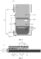
- FIG. 9 shows a sectional structural view of another display module 11 according to an embodiment of the present disclosure.
- the display module 11 includes a display panel 111, a driving circuit 112, a flexible circuit board 113 and a shielding film 114.
- the display panel 111 includes a first panel part 1111, a second panel part 1112, and a bent panel part 1113 connecting the first panel part 1111 and the second panel part 1112.
- the second panel part 1112 is located on a back surface of the first panel part 1111.
- the first panel part 1111 and the second panel part 1112 may be parallel to each other or the first panel part 1111 is substantially parallel to the second panel part 1112.
- an angle between the first panel part 1111 and the second panel part 1112 is less than 5 degrees.
- the back surface of the first panel part 1111 may be a surface, close to the second panel part 1112, of the first panel part 1111.
- the driving circuit 112 is located on a side, away from the first panel part 1111, of the second panel part 1112 and electrically connected with the display panel 111.
- the flexible circuit board 113 is located on the back surface of the first panel part 1111 and electrically connected with an end, away from the bent panel part 1113, of the second panel part 1112.
- the shielding film 114 is located on a side, away from the first panel part 1111, of the driving circuit 112.
- An orthographic projection of the shielding film 114 on the first panel part 1111 covers an orthographic projection of the driving circuit 112 on the first panel part 1111 and an orthographic projection of the flexible circuit board 113 on the first panel part 1111.
- the driving circuit 112 includes a MUX 1121 and a display IC 1122, both of which are located on a surface, away from the first panel part 1111, of the second panel part 1112.
- the display IC 1122 is electrically connected with the display panel 111 through the MUX 1121.
- a connection relationship between the MUX 1121 and the display IC 1122 and the routing principle of the MUX 1121 may refer to the foregoing display device embodiment, and will not be repeated in the embodiment of the present disclosure here.
- the flexible circuit board 113 may have two ends. One end (not labeled in FIG. 9 ) of the flexible circuit board 113 is electrically connected with an end, away from the bent panel part 1113, of the second panel part 1112 and the other end E (not shown in FIG. 9 ) thereof is configured to be electrically connected with a client mainboard (not shown in FIG. 9 ).
- the flexible circuit board 113 includes a conductive layer 1131 and an insulating layer 1132 which are stacked.
- the conductive layer 1131 may be a copper layer.
- the insulating layer 1132 has an opening (not labeled in FIG. 9 ) and part of the conductive layer 1131 is exposed through the opening.
- the shielding film 114 may include an adhesive layer 1141 and a shielding layer 1142 which are stacked.
- the shielding film 114 is adhered to the side, away from the first panel part 1111, of the driving circuit 112 through the adhesive layer 1141.
- the shielding layer 1142 includes one or more of a conductive fabric, copper foil and aluminum foil.
- the adhesive layer 1141 includes a first conductive portion x and an insulating partition y. An orthographic projection of the first conductive portion x on the first panel part 1111 overlaps with an orthographic projection of the opening of the flexible circuit board 113 on the first panel part 1111.
- the shielding film 114 is grounded.
- the orthographic projection of the first conductive portion x on the first panel part 1111 may cover the orthographic projection of the opening of the flexible circuit board 113 on the first panel part 1111. As such, it is convenient for a sufficient contact of the first conductive portion x with the conductive layer 1131and thus ensuring the effective connection of the shielding film 114 with the flexible circuit board 113.
- the display module 11 further includes a heat-dissipating film 115 located between the first panel part 1111 and the second panel part 1112 and between the first panel part 1111 and the flexible circuit board 113, and part of the heat-dissipating film 115 is in contact with the second panel part 1112 and the flexible circuit board 113.
- the adhesive layer 1141 further includes a second conductive portion z. The first conductive portion x is electrically connected with the second conductive portion z (not shown in FIG. 9 ).
- the shielding film 114 is electrically connected with the heat-dissipating film 115 through the second conductive portion z.
- the heat-dissipating film 115 may be made of metal.
- the heat-dissipating film 115 is copper foil. In an operation process of the display module 11, the driving circuit 112 and the flexible circuit board 113 likely generate heat.
- the heat generated by the driving circuit 112 may be transferred to the heat-dissipating film 115 through the second panel part 1112 and then is dissipated from the display module 11 by the heat-dissipating film 115.
- the heat generated by the flexible circuit board 113 may be directly transferred to the heat-dissipating film 115 and then is dissipated from the display module 11 by the heat-dissipating film 115. Therefore, the heat-dissipating film 115 may effectively dissipate the heat generated by the display module 11.
- the display module 11 further includes a buffer layer 116 located between the heat-dissipating film 115 and the first panel part 1111.
- the buffer layer 116 may be a foam layer.
- the buffer layer 116 may buffer the heat-dissipating film 115 and other structures to reduce stress of the heat-dissipating film 115 and other structures.
- the display module includes the shielding film and the driving circuit, and the shielding film may shield the interference signal generated by the driving circuit.
- the influence of the interference signal on a display signal of the display module may be decreased.
- FIG. 10 shows a method flow chart of a method for manufacturing a display device according to an embodiment of the present disclosure.
- the method for manufacturing the display device may be applied to manufacture the display device 0 shown in FIG. 1 , FIG. 7 or FIG. 8 .
- the method includes the following steps.
- step 101 a middle frame antenna is manufactured.
- the middle frame antenna may have different forms.
- the middle frame antenna 02 includes an upper antenna 021, a lower antenna 022 and a side antenna 023.
- the upper antenna 021 is of a U-shaped structure.
- the upper antenna 021 includes a bottom edge 0211 and two side edges 0212 located at two ends of the bottom edge.
- the lower antenna 022 is of a U-shaped structure.
- the lower antenna 022 includes a bottom edge 0221 and two side edges 0222 located at two ends of the bottom edge 0221.
- the side antenna 023 is of a linear structure.
- the middle frame antenna 02 includes an upper antenna 021 and a lower antenna 022.
- the upper antenna 021 is of an L-shaped structure.
- the upper antenna 021 includes a first edge 0211 and a second edge 0212.
- the first edge 0211 has a length greater than that of the second edge 0212.
- the lower antenna 022 is of a U-shaped structure.
- the lower antenna 022 includes a bottom edge 0221 and two side edges 0222 located at two ends of the bottom edge.
- the middle frame antenna 02 includes two upper antennas 021 and a lower antenna 022.
- the upper antenna 021 is of a linear structure.
- the lower antenna 022 is of a U-shaped structure.
- the lower antenna 022 includes a bottom edge 0221 and two side edges 0222 located at two ends of the bottom edge 0221.
- the middle frame antenna may be made of metal material or alloy material.
- the middle frame antenna may be made of aluminum alloy material.
- the middle frame antenna may be manufactured by a metal forming process.
- the middle frame antenna 02 shown in FIG. 1 , FIG. 7 or FIG. 8 may be manufactured by the metal forming process.
- a display panel is manufactured, wherein the display panel includes a first panel part, a second panel part, and a connection panel part connecting the first panel part and the second panel part.
- the display panel may be a flexible display panel, so that the display panel may be bent along the connection panel part.
- the second panel part is located on a back surface of the first panel part.
- the display panel may be an organic light-emitting diode (OLED) display panel or a quantum dot light-emitting diode (QLED) display panel.
- OLED organic light-emitting diode
- QLED quantum dot light-emitting diode
- a driving circuit is manufactured, wherein the driving circuit includes a multiplexer and a display integrated circuit.
- the multiplexer may be a 1:n MUX. That is, each input port in the MUX corresponds to n output ports, where n is an integer greater than 1.
- the multiplexer may be a 1:2 MUX.
- the display integrated circuit may be a display integrated IC.
- the multiplexer and the display integrated circuit may be manufactured by a circuit preparation process, so that the driving circuit is manufactured.
- a flexible circuit board is manufactured, wherein the flexible circuit board includes a conductive layer and an insulating layer which are stacked.
- the insulating layer has an opening and part of the conductive layer is exposed through the opening.
- the conductive layer may be made of metal material or alloy material.
- the conductive layer may be made of one of copper, aluminum and molybdenum or alloy material of at least two of copper, aluminum and molybdenum.
- the insulating layer may be made of one of SiO 2 , SiOx, SiNx, Al 2 O 3 and SiOxNx or a combination thereof.
- a metal copper material layer may be formed by any of processes such as sputtering and thermal evaporation, and then is processed by a one-time patterning process to obtain the conductive layer.
- a SiOz material layer is formed on the conductive layer by any of processes such as deposition, coating and sputtering and then is processed to obtain the insulating layer having the opening.
- the flexible circuit board is obtained.
- step 105 a buffer layer is manufactured.
- the buffer layer may be a foam layer.
- step 106 a heat-dissipating film is manufactured.
- the heat-dissipating film may be made of metal.
- the heat-dissipating film may be copper foil.
- the heat-dissipating film may be manufactured with metal copper as material by a film forming process.
- a shielding film is manufactured, wherein the shielding film includes an adhesive layer and a shielding layer which are stacked.
- the adhesive layer includes a first conductive portion, a second conductive portion and an insulating portion except the first conductive portion and the second conductive portion.
- the first conductive portion is electrically connected with the second conductive portion.
- the shielding layer may include one or more of a conductive fabric, copper foil and aluminum foil.
- the shielding layer is a conductive fabric.
- the adhesive layer includes a first conductive portion, a second conductive portion and an insulating portion except the first conductive portion and the second conductive portion. The first conductive portion is electrically connected with the second conductive portion.
- the first conductive portion and the second conductive portion may be formed on a base substrate by a conductive adhesive and the insulating portion is formed on the base substrate by an insulating adhesive, and the first conductive portion and the second conductive portion are electrically connected, thereby obtaining the adhesive layer.
- the conductive fabric, copper foil and aluminum foil are formed on the adhesive layer to obtain the shielding layer.
- the base substrate is removed to obtain the shielding film.
- step 108 a wave-absorbing layer is formed on the back surface of the first panel part.
- the shape of the wave-absorbing layer may vary according to different forms of the middle frame antenna.
- the wave-absorbing layer 012 is irregularly polygonal.
- the wave-absorbing layer 012 is L-shaped.
- the wave-absorbing layer 012 is T-shaped.
- the wave-absorbing layer may be made of one or more of ferrite, magnetic iron nanomaterial, silicon carbide and a graphene polymer.
- a ferrite material layer may be formed on the back surface of the first panel part by any of processes such as deposition, coating and sputtering, and then is processed by the one-time patterning process to obtain the wave-absorbing layer.
- the wave-absorbing layer 012 shown in FIG. 1 , FIG. 7 or FIG. 8 is obtained by processing the ferrite material layer by the one-time patterning process.
- the buffer layer is disposed on the back surface of the first panel part, so that the buffer layer is distributed on the same layer as the wave-absorbing layer.
- the buffer layer may be adhered to the back surface of the first panel part with an optical adhesive, so that the buffer layer is distributed on the same layer as the wave-absorbing layer.
- the heat-dissipating film is disposed on a side, away from the first panel part, of the buffer layer and the wave-absorbing layer.
- the heat-dissipating film may be adhered to the side, away from the first panel part, of the buffer layer and the wave-absorbing layer with an optical adhesive.
- An orthographic projection of the heat-dissipating film on the first panel part covers an orthographic projection of the buffer layer on the first panel part and an orthographic projection of the wave-absorbing layer on the first panel part.
- step 111 the driving circuit is disposed on a surface, away from the back surface of the first panel part, of the second panel part, so that the display integrated circuit is electrically connected with the display panel through the multiplexer.
- the MUX may be electrically connected with the display panel and the display IC is electrically connected with the MUX, and then the display IC and the MUX are adhered to the surface, away from the back surface of the first panel part, of the second panel part.
- a connection relationship between the MUX and the display panel and a connection relationship between the display IC and the MUX may refer to FIGS. 4-6 , and will not be repeated in the embodiment of the present disclosure here.
- one end of the flexible circuit board is electrically connected with an end, away from the first panel part, of the second panel part, so that the conductive layer of the flexible circuit board is close to the back surface of the first panel part.
- one end of the flexible circuit board and the end, away from the first panel part, of the second panel part may be both provided with a golden finger.
- One end of the flexible circuit board is bound to the end, away from the first panel part, of the second panel part through the golden fingers, so that the one end of the flexible circuit board is electrically connected with the end, away from the first panel part, of the second panel part and the conductive layer of the flexible circuit board is close to the back surface of the first panel part.
- step 113 the second panel part is bent to the back surface of the first panel part along the connection panel part.
- the second panel part may be bent to the back surface of the first panel part along the connection panel part.
- the driving circuit is located on a side, away from the first panel part, of the second panel part; the flexible circuit board is located on the back surface of the first panel part; the wave-absorbing layer and the buffer layer are located between the first panel part and the second panel part; the heat-dissipating film is located between the first panel part and the second panel part, and between the first panel part and the flexible circuit board, and part of the heat-dissipating film is in contact with the second panel part and the flexible circuit board; and an orthographic projection of the driving circuit on the first panel part, an orthographic projection of the flexible circuit board on the first panel part, and an orthographic projection of the wave-absorbing layer on the first panel part do not overlap.
- step 114 the shielding film is disposed on a side, away from the first panel part, of the driving circuit to obtain a display module.
- the shielding film may be adhered to the side, away from the first panel part, of the driving circuit through the adhesive layer of the shielding film by an adhering process.
- an orthographic projection of the first conductive portion of the adhesive layer in the shielding film on the first panel part overlaps with an orthographic projection of the opening of the flexible circuit board on the first panel part
- an orthographic projection of the second conductive portion on the first panel part overlaps with a portion, not in contact with the flexible circuit board and the second panel part, of the heat-dissipating film
- the shielding film is electrically connected with the flexible circuit board through the first conductive portion and electrically connected with the heat-dissipating film through the second conductive portion, and the shielding film is grounded;
- an orthographic projection of the shielding film on the first panel part covers an orthographic projection of the driving circuit on the first panel part and an orthographic projection of the flexible circuit board on the first panel part, and the orthographic projection of the shielding film on the first panel part does not overlap with the
- the middle frame antenna is disposed around the display module, so that a minimum distance between the boundary of the wave-absorbing layer and the middle frame antenna is greater than or equal to 8 millimeters.
- the middle frame antenna 02 may be disposed around the display module 01.
- the upper antenna 021 is located at the top of the display module 01, the bottom edge 0211 of the upper antenna 021 extends along a top edge of the display module 01 and the two side edges 0212 of the upper antenna 021 extend along two side edges of the display module 01;
- the lower antenna 022 is located at the bottom of the display module 01, the bottom edge 0221 of the lower antenna 022 extends along a bottom edge of the display module 01 and the two side edges 0222 of the lower antenna 022 extend along two side edges of the display module 01;
- the side antenna 023 extends along the side edge of the display module 01 and located between the upper antenna 021 and the lower antenna 022;
- a minimum distance d1 between the boundary of the wave-absorbing layer 012 and the upper antenna 021 and a minimum distance d3 between the boundary of the wave-absorbing layer 012 and the side antenna 023 may be greater than or equal to 8 millimeters; the minimum distance d1 between the boundary of the wave-absorbing layer 012 and the upper antenna 021 is equal to the minimum distance
- the middle frame antenna 02 may be disposed around the display module 01.
- the upper antenna 021 is located at the top of the display module 01, the first edge 0211 of the upper antenna 021 extends along a top edge of the display module 01 and the second edge 0212 extends along one side edge of the display module 01;
- the lower antenna 022 is located at the bottom of the display module 01, the bottom edge 0221 of the lower antenna 022 extends along a bottom edge of the display module 01 and the two side edges 0222 of the lower antenna 022 extend along two side edges of the display module 01;
- a minimum distance d1 between the boundary of the wave-absorbing layer 012 and the upper antenna 021 may be greater than or equal to 8 millimeters; and a minimum distance d2 between the boundary of the wave-absorbing layer 012 and the lower antenna 022 may be greater than 8 millimeters.
- the middle frame antenna 02 may be disposed around the display module 01.
- the two upper antennas 021 are located at the top of the display module 01 and extend along two side edges of the display module 01respectively;
- the lower antenna 022 is located at the bottom of the display module 01, the bottom edge 0221 of the lower antenna 022 extends along a bottom edge of the display module 01 and the two side edges 0222 of the lower antenna 022 extend along two side edges of the display module 01;
- a minimum distance d1 between the boundary of the wave-absorbing layer 012 and the upper antenna 021 may be greater than or equal to 8 millimeters; and a minimum distance d2 between the boundary of the wave-absorbing layer 012 and the lower antenna 022 may be greater than 8 millimeters.
- a distance between the middle frame antenna and an edge of the display module it is possible to set a distance between the middle frame antenna and an edge of the display module to be approximately 0.5 millimeter.
- the distance between the middle frame antenna and the edge of the display module is 0.51 millimeter, 0.52 millimeter, 0.49 millimeter, 0.48 millimeter or the like, which is not limited in the embodiment of the present disclosure.
- the display device manufactured by the method for manufacturing the display device includes the display module and the middle frame antenna.
- the display module includes the wave-absorbing layer and the driving circuit and the wave-absorbing layer may absorb the interference signal generated by the driving circuit. Therefore, the influence of the interference signal on a display signal of the display device can be decreased.
- the minimum distance between the boundary of the wave-absorbing layer and the middle frame antenna is greater than or equal to 8 millimeters, the wave-absorbing layer can be avoided from interfering with a signal of the middle frame antenna.
- the display module further includes the shielding film and the shielding film may shield the interference signal generated by the driving circuit. Thus, the influence of the interference signal on the display signal of the display module is decreased.
- the involved one-time patterning process includes photoresist coating, exposure, development, etching and photoresist stripping.
- the processing of a material layer (such as a metal copper material layer) by the one-time patterning process includes: firstly, coating the material layer (such as the metal copper material layer) with a layer of photoresist to form a photoresist layer; next, exposing the photoresist layer with a mask, so that the photoresist layer forms a completely-exposed region and a non-exposed region; subsequently, adopting a developing process for processing, so that the photoresist in the completely-exposed region is completely removed, and all the photoresist in the non-exposed region is retained; hereafter, etching a region, corresponding to the completely-exposed region, on the material layer (such as the metal copper material layer) by an etching process; and stripping the photoresist in the non-exposed region, so that
- the description is given by taking the photoresist as a positive photoresist.
- the process of the one-time patterning process may refer to the description in this paragraph and will not be repeated in the embodiment of the present disclosure here.
Landscapes
- Engineering & Computer Science (AREA)
- Computer Hardware Design (AREA)
- Theoretical Computer Science (AREA)
- Physics & Mathematics (AREA)
- General Physics & Mathematics (AREA)
- General Engineering & Computer Science (AREA)
- Human Computer Interaction (AREA)
- Power Engineering (AREA)
- Computer Networks & Wireless Communication (AREA)
- Condensed Matter Physics & Semiconductors (AREA)
- Microelectronics & Electronic Packaging (AREA)
- Devices For Indicating Variable Information By Combining Individual Elements (AREA)
Claims (10)
- Module d'affichage (01) pour un terminal mobile, comprenant :un panneau d'affichage (011), dans lequel le panneau d'affichage (011) comprend une première partie de panneau (0111), une seconde partie de panneau (0112) et une partie de panneau pliée (0113) reliant la première partie de panneau (0111) et la seconde partie de panneau (0112), et la seconde partie de panneau (0112) est située sur une surface arrière de la première partie de panneau (0111) ;un circuit de commande (013), dans lequel le circuit de commande (013) comprend un multiplexeur (0131) et un circuit intégré d'affichage (0132), le multiplexeur (0131) et le circuit intégré d'affichage (0132) sont tous deux situés sur une surface, à l'opposé de la première partie de panneau (0111), de la seconde partie de panneau (0112), et le circuit intégré d'affichage (0132) est électriquement connecté au panneau d'affichage (011) par l'intermédiaire du multiplexeur (0131) ;une carte de circuit imprimé flexible (014), dans lequel la carte de circuit imprimé flexible (014) est située sur la surface arrière de la première partie de panneau (0111) et une extrémité de la carte de circuit imprimé flexible (014) est connectée électriquement à une extrémité, à l'opposé de la partie de panneau pliée (0113), de la seconde partie de panneau (0112) et l'autre extrémité est configurée pour être connectée électriquement à une carte mère client ; etun film de protection (015), dans lequel le film de protection (015) est situé sur un côté, à l'opposé de la première partie de panneau (0111), du circuit de commande (013) et le film de protection (015) comprend une couche adhésive (0151) et une couche de protection (0152) qui sont empilées, le film de protection (015) est collé sur un côté, à l'opposé de la première partie de panneau (0111), du circuit de commande (013) par l'intermédiaire de la couche adhésive (0151), et une projection orthographique du film de protection (015) sur la première partie de panneau (0111) recouvre une projection orthographique du circuit de commande (013) sur la première partie de panneau (0111) et une projection orthographique de la carte de circuit imprimé flexible (014) sur la première partie de panneau (0111) ; et la projection orthographique du film de protection (015) sur la première partie de panneau (0111) ne chevauche pas la projection orthographique d'une couche absorbant les ondes (012) sur la première partie de panneau (0111),dans lequel le module d'affichage (01) comprend en outre un film dissipateur de chaleur (016) situé entre la première partie de panneau (0111) et la seconde partie de panneau (0112), et entre la première partie de panneau (0111) et la carte de circuit imprimé flexible (014), et une partie du film de dissipation de chaleur (016) est en contact avec la seconde partie de panneau (0112) et la carte de circuit imprimé flexible (014) ;une extrémité de la carte de circuit imprimé flexible (014) est connectée électriquement à l'extrémité, à l'opposé de la partie de panneau pliée (0113), de la seconde partie de panneau (0112) et l'autre extrémité est configurée pour être connectée électriquement à la carte mère client, la carte de circuit imprimé flexible (014) comprend une couche conductrice (0141) et une couche isolante (0142) qui sont empilées, et la couche isolante (0142) possède une ouverture et une partie de la couche conductrice (0141) est exposée à travers l'ouverture ;dans le film de protection (015), la couche adhésive (0151) comprend une première partie conductrice (a), une seconde partie conductrice (b) et une partie isolante (c), à l'exception de la première partie conductrice (a) et de la seconde partie conductrice (b), la première partie conductrice (a) est connectée électriquement à la seconde partie conductrice (b), une projection orthographique de la première partie conductrice (a) sur la première partie de panneau (0111) chevauche une projection orthographique de l'ouverture sur la première partie de panneau (0111), et une projection orthographique de la seconde partie conductrice (b) sur la première partie de panneau (0111) chevauche une partie qui n'est pas en contact avec la carte de circuit imprimé flexible (014) et la seconde partie de panneau (0112), du film dissipateur de chaleur (016) ; etle film de protection (015) est connecté électriquement à la carte de circuit imprimé flexible (014) par l'intermédiaire de la première partie conductrice (a) et est connecté électriquement au film de dissipation de chaleur (016) par l'intermédiaire de la seconde partie conductrice (b), et le film de protection (015) est mis à la terre.
- Dispositif d'affichage pour un terminal mobile, comprenant : un module d'affichage (01) et une antenne cadre médiane (02) située autour du module d'affichage (01),dans lequel le module d'affichage (01) est le module d'affichage (01) selon la revendication 1, etdans lequel la couche absorbant les ondes (012) est située sur la première partie de panneau (0111), et une distance minimale entre une limite de la couche absorbant les ondes (012) et l'antenne cadre médiane (02) est supérieure ou égale à 8 millimètres ; etdans lequel une projection orthographique du circuit de commande (013) sur la première partie de panneau (0111), une projection orthographique de la carte de circuit imprimé flexible (014) sur la première partie de panneau (0111) et une projection orthographique de la couche absorbant les ondes (012) sur la première partie de panneau (0111) ne se chevauchent pas.
- Dispositif d'affichage selon la revendication 2, dans lequel
le module d'affichage (01) comprend en outre une couche tampon (117) située entre le film de dissipation de chaleur (016) et la première partie de panneau (0111) et répartie sur la même couche que la couche absorbant les ondes (012). - Dispositif d'affichage selon l'une quelconque des revendications 2 à 3, dans lequel la distance minimale entre la limite de la couche absorbant les ondes (012) et l'antenne cadre médiane (02) est supérieure ou égale à 10 millimètres.
- Dispositif d'affichage selon l'une quelconque des revendications 2 à 4, dans lequel
une distance minimale entre un point d'extrémité de l'antenne cadre médiane (02) et un point d'extrémité de la couche absorbant les ondes (012) est supérieure ou égale à 10 millimètres. - Dispositif d'affichage selon l'une quelconque des revendications 2 à 5, dans lequell'antenne cadre médiane (02) comprend une antenne supérieure (021), une antenne inférieure (022) et une antenne latérale (023), et une structure de l'antenne supérieure (021) est la même que celle de l'antenne inférieure (022) ;l'antenne supérieure (021) est d'une structure en forme de U et comprend un bord inférieur (0211) et deux bords latéraux (0212) situés aux deux extrémités du bord inférieur (0211) ; l'antenne supérieure (021) est située en haut du module d'affichage (01), le bord inférieur (0211) de l'antenne supérieure (021) s'étend le long d'un bord supérieur du module d'affichage (01) et les deux bords latéraux (0212) de l'antenne supérieure (021) s'étendent le long de deux bords latéraux (0212) du module d'affichage (01) ;l'antenne inférieure (022) est située en bas du module d'affichage (01), un bord inférieur (0221) de l'antenne inférieure (022) s'étend le long d'un bord inférieur du module d'affichage (01) et deux bords latéraux (0222) de l'antenne inférieure (022) s'étendent le long des deux bords latéraux (0222) du module d'affichage (01) ;l'antenne latérale (023) est d'une structure linéaire, s'étend le long du bord latéral du module d'affichage (01) et est située entre l'antenne supérieure (021) et l'antenne inférieure (022) ; etune distance minimale entre la limite de la couche absorbant les ondes (012) et l'antenne supérieure (021) et une distance minimale entre la limite de la couche absorbant les ondes (012) et l'antenne latérale (023) sont supérieures ou égales à 8 millimètres, et une distance minimale entre la limite de la couche absorbant les ondes (012) et l'antenne inférieure (022) est supérieure à 8 millimètres.
- Dispositif d'affichage selon la revendication 6, dans lequel
la distance minimale entre la limite de la couche absorbant les ondes (012) et l'antenne supérieure (021) est égale à la distance minimale entre la limite de la couche absorbant les ondes (012) et l'antenne latérale (023). - Dispositif d'affichage selon l'une quelconque des revendications 2 à 5, dans lequell'antenne cadre médiane (02) comprend une antenne supérieure (021) et une antenne inférieure (022),l'antenne supérieure (021) est d'une structure en forme de L, comprend un premier bord (0211) et un second bord (0212), et une longueur du premier bord (0211) est supérieure à celle du second bord (0212) ;l'antenne inférieure (022) est d'une structure en forme de U et comprend un bord inférieur (0221) et deux bords latéraux (0222) situés aux deux extrémités du bord inférieur (0221) ; l'antenne supérieure (021) est située en haut du module d'affichage (01), le premier bord (0211) s'étend le long d'un bord supérieur du module d'affichage (01) et le second bord (0212) s'étend le long d'un bord latéral du module d'affichage (01) ;l'antenne inférieure (022) est située en bas du module d'affichage (01), un bord inférieur (0221) de l'antenne inférieure (022) s'étend le long d'un bord inférieur (0221) du module d'affichage (01) et deux bords latéraux (0222) de l'antenne inférieure (022) s'étendent le long de deux bords latéraux (0222) du module d'affichage (01) ; etla couche absorbant les ondes (012) est en forme de L, une distance minimale entre la limite de la couche absorbant les ondes (012) et l'antenne supérieure (021) est supérieure ou égale à 8 millimètres, et une distance minimale entre la limite de la couche absorbant les ondes (012) et l'antenne inférieure (022) est supérieure à 8 millimètres.
- Dispositif d'affichage selon l'une quelconque des revendications 2 à 5, dans lequell'antenne cadre médiane (02) comprend une antenne inférieure (022) et deux antennes supérieures (021) ;l'antenne supérieure (021) est d'une structure linéaire ; l'antenne inférieure (022) est d'une structure en forme de U et comprend un bord inférieur (0221) et deux bords latéraux (0222) situés aux deux extrémités du bord inférieur (0221) ;les deux antennes supérieures (021) sont situées en haut du module d'affichage (01) et s'étendent respectivement le long de deux bords latéraux (0212) du module d'affichage (01) ; l'antenne inférieure (022) est située en bas du module d'affichage (01), un bord inférieur (0221) de l'antenne inférieure (022) s'étend le long d'un bord inférieur (0221) du module d'affichage (01) et deux bords latéraux (0222) de l'antenne inférieure (022) s'étendent le long des deux bords latéraux (0222) du module d'affichage (01) ; etla couche absorbant les ondes (012) est en forme de T, une distance minimale entre la limite de la couche absorbant les ondes (012) et l'antenne supérieure (021) est supérieure ou égale à 8 millimètres, et une distance minimale entre la limite de la couche absorbant les ondes (012) et l'antenne inférieure (022) est supérieure à 8 millimètres.
- Dispositif d'affichage selon l'une quelconque des revendications 2 à 9, dans lequel le dispositif d'affichage est un terminal mobile.
Applications Claiming Priority (1)
| Application Number | Priority Date | Filing Date | Title |
|---|---|---|---|
| PCT/CN2019/098337 WO2021016848A1 (fr) | 2019-07-30 | 2019-07-30 | Appareil d'affichage et module d'affichage |
Publications (3)
| Publication Number | Publication Date |
|---|---|
| EP4006984A1 EP4006984A1 (fr) | 2022-06-01 |
| EP4006984A4 EP4006984A4 (fr) | 2022-08-17 |
| EP4006984B1 true EP4006984B1 (fr) | 2024-05-08 |
Family
ID=74228399
Family Applications (1)
| Application Number | Title | Priority Date | Filing Date |
|---|---|---|---|
| EP19933240.4A Active EP4006984B1 (fr) | 2019-07-30 | 2019-07-30 | Appareil d'affichage et module d'affichage |
Country Status (4)
| Country | Link |
|---|---|
| US (1) | US11270635B2 (fr) |
| EP (1) | EP4006984B1 (fr) |
| CN (1) | CN112585760B (fr) |
| WO (1) | WO2021016848A1 (fr) |
Families Citing this family (6)
| Publication number | Priority date | Publication date | Assignee | Title |
|---|---|---|---|---|
| CN111651096B (zh) * | 2020-07-22 | 2023-06-23 | 京东方科技集团股份有限公司 | 一种显示装置 |
| CN112951093B (zh) * | 2021-02-10 | 2022-12-13 | 厦门天马微电子有限公司 | 显示模组和显示装置 |
| CN113594211A (zh) * | 2021-07-28 | 2021-11-02 | 京东方科技集团股份有限公司 | 显示装置及其制造方法 |
| CN114035704B (zh) * | 2021-11-05 | 2023-07-18 | 业成科技(成都)有限公司 | 电路板结构、背光模组、显示模组及触控显示模组 |
| WO2023090848A1 (fr) * | 2021-11-16 | 2023-05-25 | 삼성전자 주식회사 | Dispositif électronique comprenant une antenne |
| CN114401356B (zh) * | 2022-01-21 | 2023-04-18 | 武汉华星光电半导体显示技术有限公司 | 显示装置 |
Family Cites Families (11)
| Publication number | Priority date | Publication date | Assignee | Title |
|---|---|---|---|---|
| JP2000112392A (ja) * | 1998-09-30 | 2000-04-21 | Sony Corp | ディスプレイ装置 |
| US8872764B2 (en) | 2012-06-29 | 2014-10-28 | Qualcomm Mems Technologies, Inc. | Illumination systems incorporating a light guide and a reflective structure and related methods |
| CN105824460B (zh) | 2016-03-10 | 2019-04-05 | 昆山维信诺科技有限公司 | Oled显示面板及制作方法 |
| KR101796660B1 (ko) * | 2016-04-19 | 2017-11-10 | 삼성전자주식회사 | 지문 인식 기능을 지원하는 전자 장치 및 이의 운용 방법 |
| CN106252380B (zh) * | 2016-08-31 | 2020-04-03 | 上海天马有机发光显示技术有限公司 | 柔性显示面板及装置 |
| WO2018057651A1 (fr) * | 2016-09-22 | 2018-03-29 | Apple Inc. | Ensemble de distribution thermique dans un dispositif électronique |
| JP2018054736A (ja) * | 2016-09-27 | 2018-04-05 | 株式会社ジャパンディスプレイ | 表示装置 |
| CN107454215B (zh) | 2017-07-28 | 2020-12-04 | 捷开通讯(深圳)有限公司 | 防止耦合灵敏度恶化的移动终端 |
| KR102508668B1 (ko) * | 2017-11-24 | 2023-03-13 | 삼성디스플레이 주식회사 | 표시장치 및 이의 제조방법 |
| KR20190066795A (ko) * | 2017-12-06 | 2019-06-14 | 삼성전자주식회사 | 디스플레이와 초음파 센서 사이에 디스플레이에서 발생된 노이즈를 차단하기 위한 도전성 부재가 배치된 전자 장치 |
| CN208570937U (zh) * | 2018-06-06 | 2019-03-01 | Oppo广东移动通信有限公司 | 显示屏组件及电子设备 |
-
2019
- 2019-07-30 US US16/771,252 patent/US11270635B2/en active Active
- 2019-07-30 WO PCT/CN2019/098337 patent/WO2021016848A1/fr unknown
- 2019-07-30 CN CN201980001186.3A patent/CN112585760B/zh active Active
- 2019-07-30 EP EP19933240.4A patent/EP4006984B1/fr active Active
Also Published As
| Publication number | Publication date |
|---|---|
| EP4006984A4 (fr) | 2022-08-17 |
| WO2021016848A1 (fr) | 2021-02-04 |
| EP4006984A1 (fr) | 2022-06-01 |
| US20210407389A1 (en) | 2021-12-30 |
| CN112585760A (zh) | 2021-03-30 |
| US11270635B2 (en) | 2022-03-08 |
| CN112585760B (zh) | 2024-05-14 |
Similar Documents
| Publication | Publication Date | Title |
|---|---|---|
| EP4006984B1 (fr) | Appareil d'affichage et module d'affichage | |
| US11121201B2 (en) | Display device | |
| WO2020216259A1 (fr) | Panneau d'affichage, dispositif d'affichage et procédé de fabrication | |
| US20190221782A1 (en) | Display panel, manufacturing method thereof, and display device | |
| TW201712495A (zh) | 具天線之觸控面板 | |
| US20190034012A1 (en) | Touch substrate, manufacturing method thereof and touch device | |
| US20140146004A1 (en) | Input device | |
| US12039116B2 (en) | Radio frequency shielding using a touch on encapsulation layer | |
| EP4145515A1 (fr) | Dispositif d'affichage électroluminescent organique et son procédé de fabrication | |
| CN109358770B (zh) | 触控面板及其制造方法、触控显示装置 | |
| US20180217464A1 (en) | Pixel unit, array substrate, and display device, and fabrication methods thereof | |
| CN110851016A (zh) | 一种触控基板及其制备方法、触控装置 | |
| CN109524421A (zh) | 转接基板及其制造方法、阵列基板及显示装置 | |
| CN111430428A (zh) | 柔性显示面板及其制作方法、显示装置 | |
| US9678588B2 (en) | Wire-bonded borderless display | |
| JP2004187065A (ja) | 表示装置 | |
| CN112102739A (zh) | 一种电子设备 | |
| CN114171896B (zh) | 显示模组及显示装置 | |
| CN217521580U (zh) | 触控基板、触控显示面板和触控显示装置 | |
| US20240298483A1 (en) | Display apparatus and manufacturing method thereof | |
| EP4220295A1 (fr) | Dispositif électronique | |
| CN116009718A (zh) | 触控基板及其制备方法、触控显示面板和触控显示装置 | |
| TWM514051U (zh) | 具天線之觸控面板 | |
| CN114138135A (zh) | 一种触控发光面板、制备方法以及触控发光装置 | |
| CN113849079A (zh) | 显示面板及显示装置 |
Legal Events
| Date | Code | Title | Description |
|---|---|---|---|
| STAA | Information on the status of an ep patent application or granted ep patent |
Free format text: STATUS: UNKNOWN |
|
| STAA | Information on the status of an ep patent application or granted ep patent |
Free format text: STATUS: THE INTERNATIONAL PUBLICATION HAS BEEN MADE |
|
| PUAI | Public reference made under article 153(3) epc to a published international application that has entered the european phase |
Free format text: ORIGINAL CODE: 0009012 |
|
| STAA | Information on the status of an ep patent application or granted ep patent |
Free format text: STATUS: REQUEST FOR EXAMINATION WAS MADE |
|
| 17P | Request for examination filed |
Effective date: 20201223 |
|
| AK | Designated contracting states |
Kind code of ref document: A1 Designated state(s): AL AT BE BG CH CY CZ DE DK EE ES FI FR GB GR HR HU IE IS IT LI LT LU LV MC MK MT NL NO PL PT RO RS SE SI SK SM TR |
|
| A4 | Supplementary search report drawn up and despatched |
Effective date: 20220720 |
|
| RIC1 | Information provided on ipc code assigned before grant |
Ipc: G09G 3/20 20060101ALI20220714BHEP Ipc: G06F 1/20 20060101ALI20220714BHEP Ipc: G06F 1/16 20060101ALI20220714BHEP Ipc: H01L 27/12 20060101ALI20220714BHEP Ipc: H01L 27/32 20060101AFI20220714BHEP |
|
| DAV | Request for validation of the european patent (deleted) | ||
| DAX | Request for extension of the european patent (deleted) | ||
| REG | Reference to a national code |
Ref country code: DE Ref legal event code: R079 Ref document number: 602019052123 Country of ref document: DE Free format text: PREVIOUS MAIN CLASS: H01L0027320000 Ipc: G06F0001160000 Ref country code: DE Ref legal event code: R079 Free format text: PREVIOUS MAIN CLASS: H01L0027320000 Ipc: G06F0001160000 |
|
| GRAP | Despatch of communication of intention to grant a patent |
Free format text: ORIGINAL CODE: EPIDOSNIGR1 |
|
| STAA | Information on the status of an ep patent application or granted ep patent |
Free format text: STATUS: GRANT OF PATENT IS INTENDED |
|
| RIC1 | Information provided on ipc code assigned before grant |
Ipc: H01L 27/12 20060101ALI20231207BHEP Ipc: G09G 3/20 20060101ALI20231207BHEP Ipc: G06F 1/20 20060101ALI20231207BHEP Ipc: G06F 1/16 20060101AFI20231207BHEP |
|
| INTG | Intention to grant announced |
Effective date: 20240108 |
|
| GRAS | Grant fee paid |
Free format text: ORIGINAL CODE: EPIDOSNIGR3 |
|
| GRAA | (expected) grant |
Free format text: ORIGINAL CODE: 0009210 |
|
| STAA | Information on the status of an ep patent application or granted ep patent |
Free format text: STATUS: THE PATENT HAS BEEN GRANTED |
|
| AK | Designated contracting states |
Kind code of ref document: B1 Designated state(s): AL AT BE BG CH CY CZ DE DK EE ES FI FR GB GR HR HU IE IS IT LI LT LU LV MC MK MT NL NO PL PT RO RS SE SI SK SM TR |
|
| REG | Reference to a national code |
Ref country code: GB Ref legal event code: FG4D |
|
| REG | Reference to a national code |
Ref country code: CH Ref legal event code: EP |
|
| REG | Reference to a national code |
Ref country code: DE Ref legal event code: R096 Ref document number: 602019052123 Country of ref document: DE |
|
| REG | Reference to a national code |
Ref country code: IE Ref legal event code: FG4D |
|
| REG | Reference to a national code |
Ref country code: LT Ref legal event code: MG9D |
|
| REG | Reference to a national code |
Ref country code: NL Ref legal event code: MP Effective date: 20240508 |