EP4006969A2 - Gestapelte ausfächerungspackungsstruktur - Google Patents
Gestapelte ausfächerungspackungsstruktur Download PDFInfo
- Publication number
- EP4006969A2 EP4006969A2 EP22150096.0A EP22150096A EP4006969A2 EP 4006969 A2 EP4006969 A2 EP 4006969A2 EP 22150096 A EP22150096 A EP 22150096A EP 4006969 A2 EP4006969 A2 EP 4006969A2
- Authority
- EP
- European Patent Office
- Prior art keywords
- molding compound
- sidewall
- semiconductor die
- rdl
- rdl structure
- Prior art date
- Legal status (The legal status is an assumption and is not a legal conclusion. Google has not performed a legal analysis and makes no representation as to the accuracy of the status listed.)
- Pending
Links
Images


Classifications
-
- H—ELECTRICITY
- H10—SEMICONDUCTOR DEVICES; ELECTRIC SOLID-STATE DEVICES NOT OTHERWISE PROVIDED FOR
- H10W—GENERIC PACKAGES, INTERCONNECTIONS, CONNECTORS OR OTHER CONSTRUCTIONAL DETAILS OF DEVICES COVERED BY CLASS H10
- H10W74/00—Encapsulations, e.g. protective coatings
- H10W74/10—Encapsulations, e.g. protective coatings characterised by their shape or disposition
- H10W74/111—Encapsulations, e.g. protective coatings characterised by their shape or disposition the semiconductor body being completely enclosed
- H10W74/129—Encapsulations, e.g. protective coatings characterised by their shape or disposition the semiconductor body being completely enclosed forming a chip-scale package [CSP]
-
- H—ELECTRICITY
- H10—SEMICONDUCTOR DEVICES; ELECTRIC SOLID-STATE DEVICES NOT OTHERWISE PROVIDED FOR
- H10W—GENERIC PACKAGES, INTERCONNECTIONS, CONNECTORS OR OTHER CONSTRUCTIONAL DETAILS OF DEVICES COVERED BY CLASS H10
- H10W74/00—Encapsulations, e.g. protective coatings
- H10W74/10—Encapsulations, e.g. protective coatings characterised by their shape or disposition
- H10W74/131—Encapsulations, e.g. protective coatings characterised by their shape or disposition the semiconductor body being only partially enclosed
-
- H—ELECTRICITY
- H10—SEMICONDUCTOR DEVICES; ELECTRIC SOLID-STATE DEVICES NOT OTHERWISE PROVIDED FOR
- H10W—GENERIC PACKAGES, INTERCONNECTIONS, CONNECTORS OR OTHER CONSTRUCTIONAL DETAILS OF DEVICES COVERED BY CLASS H10
- H10W70/00—Package substrates; Interposers; Redistribution layers [RDL]
- H10W70/60—Insulating or insulated package substrates; Interposers; Redistribution layers
-
- H—ELECTRICITY
- H10—SEMICONDUCTOR DEVICES; ELECTRIC SOLID-STATE DEVICES NOT OTHERWISE PROVIDED FOR
- H10W—GENERIC PACKAGES, INTERCONNECTIONS, CONNECTORS OR OTHER CONSTRUCTIONAL DETAILS OF DEVICES COVERED BY CLASS H10
- H10W70/00—Package substrates; Interposers; Redistribution layers [RDL]
- H10W70/60—Insulating or insulated package substrates; Interposers; Redistribution layers
- H10W70/611—Insulating or insulated package substrates; Interposers; Redistribution layers for connecting multiple chips together
- H10W70/614—Insulating or insulated package substrates; Interposers; Redistribution layers for connecting multiple chips together the multiple chips being integrally enclosed
-
- H—ELECTRICITY
- H10—SEMICONDUCTOR DEVICES; ELECTRIC SOLID-STATE DEVICES NOT OTHERWISE PROVIDED FOR
- H10W—GENERIC PACKAGES, INTERCONNECTIONS, CONNECTORS OR OTHER CONSTRUCTIONAL DETAILS OF DEVICES COVERED BY CLASS H10
- H10W90/00—Package configurations
-
- H—ELECTRICITY
- H10—SEMICONDUCTOR DEVICES; ELECTRIC SOLID-STATE DEVICES NOT OTHERWISE PROVIDED FOR
- H10W—GENERIC PACKAGES, INTERCONNECTIONS, CONNECTORS OR OTHER CONSTRUCTIONAL DETAILS OF DEVICES COVERED BY CLASS H10
- H10W90/00—Package configurations
- H10W90/701—Package configurations characterised by the relative positions of pads or connectors relative to package parts
-
- H—ELECTRICITY
- H10—SEMICONDUCTOR DEVICES; ELECTRIC SOLID-STATE DEVICES NOT OTHERWISE PROVIDED FOR
- H10W—GENERIC PACKAGES, INTERCONNECTIONS, CONNECTORS OR OTHER CONSTRUCTIONAL DETAILS OF DEVICES COVERED BY CLASS H10
- H10W70/00—Package substrates; Interposers; Redistribution layers [RDL]
- H10W70/01—Manufacture or treatment
- H10W70/05—Manufacture or treatment of insulating or insulated package substrates, or of interposers, or of redistribution layers
- H10W70/08—Manufacture or treatment of insulating or insulated package substrates, or of interposers, or of redistribution layers by depositing layers on the chip or wafer, e.g. "chip-first" RDLs
- H10W70/09—Manufacture or treatment of insulating or insulated package substrates, or of interposers, or of redistribution layers by depositing layers on the chip or wafer, e.g. "chip-first" RDLs extending onto an encapsulation that laterally surrounds the chip or wafer, e.g. fan-out wafer level package [FOWLP] RDLs
-
- H—ELECTRICITY
- H10—SEMICONDUCTOR DEVICES; ELECTRIC SOLID-STATE DEVICES NOT OTHERWISE PROVIDED FOR
- H10W—GENERIC PACKAGES, INTERCONNECTIONS, CONNECTORS OR OTHER CONSTRUCTIONAL DETAILS OF DEVICES COVERED BY CLASS H10
- H10W70/00—Package substrates; Interposers; Redistribution layers [RDL]
- H10W70/099—Connecting interconnections to insulating or insulated package substrates, interposers or redistribution layers
-
- H—ELECTRICITY
- H10—SEMICONDUCTOR DEVICES; ELECTRIC SOLID-STATE DEVICES NOT OTHERWISE PROVIDED FOR
- H10W—GENERIC PACKAGES, INTERCONNECTIONS, CONNECTORS OR OTHER CONSTRUCTIONAL DETAILS OF DEVICES COVERED BY CLASS H10
- H10W70/00—Package substrates; Interposers; Redistribution layers [RDL]
- H10W70/60—Insulating or insulated package substrates; Interposers; Redistribution layers
- H10W70/62—Insulating or insulated package substrates; Interposers; Redistribution layers characterised by their interconnections
- H10W70/65—Shapes or dispositions of interconnections
- H10W70/654—Top-view layouts
- H10W70/655—Fan-out layouts
-
- H—ELECTRICITY
- H10—SEMICONDUCTOR DEVICES; ELECTRIC SOLID-STATE DEVICES NOT OTHERWISE PROVIDED FOR
- H10W—GENERIC PACKAGES, INTERCONNECTIONS, CONNECTORS OR OTHER CONSTRUCTIONAL DETAILS OF DEVICES COVERED BY CLASS H10
- H10W72/00—Interconnections or connectors in packages
- H10W72/01—Manufacture or treatment
- H10W72/0198—Manufacture or treatment batch processes
-
- H—ELECTRICITY
- H10—SEMICONDUCTOR DEVICES; ELECTRIC SOLID-STATE DEVICES NOT OTHERWISE PROVIDED FOR
- H10W—GENERIC PACKAGES, INTERCONNECTIONS, CONNECTORS OR OTHER CONSTRUCTIONAL DETAILS OF DEVICES COVERED BY CLASS H10
- H10W72/00—Interconnections or connectors in packages
- H10W72/071—Connecting or disconnecting
- H10W72/073—Connecting or disconnecting of die-attach connectors
-
- H—ELECTRICITY
- H10—SEMICONDUCTOR DEVICES; ELECTRIC SOLID-STATE DEVICES NOT OTHERWISE PROVIDED FOR
- H10W—GENERIC PACKAGES, INTERCONNECTIONS, CONNECTORS OR OTHER CONSTRUCTIONAL DETAILS OF DEVICES COVERED BY CLASS H10
- H10W72/00—Interconnections or connectors in packages
- H10W72/071—Connecting or disconnecting
- H10W72/073—Connecting or disconnecting of die-attach connectors
- H10W72/07302—Connecting or disconnecting of die-attach connectors using an auxiliary member
- H10W72/07304—Connecting or disconnecting of die-attach connectors using an auxiliary member the auxiliary member being temporary, e.g. a sacrificial coating
- H10W72/07307—Connecting or disconnecting of die-attach connectors using an auxiliary member the auxiliary member being temporary, e.g. a sacrificial coating the auxiliary member being a temporary substrate, e.g. a removable substrate
-
- H—ELECTRICITY
- H10—SEMICONDUCTOR DEVICES; ELECTRIC SOLID-STATE DEVICES NOT OTHERWISE PROVIDED FOR
- H10W—GENERIC PACKAGES, INTERCONNECTIONS, CONNECTORS OR OTHER CONSTRUCTIONAL DETAILS OF DEVICES COVERED BY CLASS H10
- H10W72/00—Interconnections or connectors in packages
- H10W72/20—Bump connectors, e.g. solder bumps or copper pillars; Dummy bumps; Thermal bumps
- H10W72/241—Dispositions, e.g. layouts
-
- H—ELECTRICITY
- H10—SEMICONDUCTOR DEVICES; ELECTRIC SOLID-STATE DEVICES NOT OTHERWISE PROVIDED FOR
- H10W—GENERIC PACKAGES, INTERCONNECTIONS, CONNECTORS OR OTHER CONSTRUCTIONAL DETAILS OF DEVICES COVERED BY CLASS H10
- H10W72/00—Interconnections or connectors in packages
- H10W72/851—Dispositions of multiple connectors or interconnections
- H10W72/874—On different surfaces
-
- H—ELECTRICITY
- H10—SEMICONDUCTOR DEVICES; ELECTRIC SOLID-STATE DEVICES NOT OTHERWISE PROVIDED FOR
- H10W—GENERIC PACKAGES, INTERCONNECTIONS, CONNECTORS OR OTHER CONSTRUCTIONAL DETAILS OF DEVICES COVERED BY CLASS H10
- H10W72/00—Interconnections or connectors in packages
- H10W72/90—Bond pads, in general
- H10W72/941—Dispositions of bond pads
- H10W72/9413—Dispositions of bond pads on encapsulations
-
- H—ELECTRICITY
- H10—SEMICONDUCTOR DEVICES; ELECTRIC SOLID-STATE DEVICES NOT OTHERWISE PROVIDED FOR
- H10W—GENERIC PACKAGES, INTERCONNECTIONS, CONNECTORS OR OTHER CONSTRUCTIONAL DETAILS OF DEVICES COVERED BY CLASS H10
- H10W74/00—Encapsulations, e.g. protective coatings
- H10W74/01—Manufacture or treatment
- H10W74/019—Manufacture or treatment using temporary auxiliary substrates
-
- H—ELECTRICITY
- H10—SEMICONDUCTOR DEVICES; ELECTRIC SOLID-STATE DEVICES NOT OTHERWISE PROVIDED FOR
- H10W—GENERIC PACKAGES, INTERCONNECTIONS, CONNECTORS OR OTHER CONSTRUCTIONAL DETAILS OF DEVICES COVERED BY CLASS H10
- H10W74/00—Encapsulations, e.g. protective coatings
- H10W74/10—Encapsulations, e.g. protective coatings characterised by their shape or disposition
- H10W74/111—Encapsulations, e.g. protective coatings characterised by their shape or disposition the semiconductor body being completely enclosed
- H10W74/121—Encapsulations, e.g. protective coatings characterised by their shape or disposition the semiconductor body being completely enclosed by multiple encapsulations, e.g. by a thin protective coating and a thick encapsulation
-
- H—ELECTRICITY
- H10—SEMICONDUCTOR DEVICES; ELECTRIC SOLID-STATE DEVICES NOT OTHERWISE PROVIDED FOR
- H10W—GENERIC PACKAGES, INTERCONNECTIONS, CONNECTORS OR OTHER CONSTRUCTIONAL DETAILS OF DEVICES COVERED BY CLASS H10
- H10W90/00—Package configurations
- H10W90/701—Package configurations characterised by the relative positions of pads or connectors relative to package parts
- H10W90/731—Package configurations characterised by the relative positions of pads or connectors relative to package parts of die-attach connectors
- H10W90/732—Package configurations characterised by the relative positions of pads or connectors relative to package parts of die-attach connectors between stacked chips
-
- H—ELECTRICITY
- H10—SEMICONDUCTOR DEVICES; ELECTRIC SOLID-STATE DEVICES NOT OTHERWISE PROVIDED FOR
- H10W—GENERIC PACKAGES, INTERCONNECTIONS, CONNECTORS OR OTHER CONSTRUCTIONAL DETAILS OF DEVICES COVERED BY CLASS H10
- H10W90/00—Package configurations
- H10W90/701—Package configurations characterised by the relative positions of pads or connectors relative to package parts
- H10W90/731—Package configurations characterised by the relative positions of pads or connectors relative to package parts of die-attach connectors
- H10W90/734—Package configurations characterised by the relative positions of pads or connectors relative to package parts of die-attach connectors between a chip and a stacked insulating package substrate, interposer or RDL
Definitions
- the present invention relates to a semiconductor package structure, and in particular to a stacked fan-out package structure with high reliability.
- WO 2009/009436 A2 discloses a semiconductor assembly b comprising a first semiconductor die, a first encapsulant, a redistribution structure, a second semiconductor die, a second encapsulant, and a second redistribution structure, A portion of encapsulant extends downwards covering a sidewall of the redistribution structure and of the first encapsulant.
- a package microelectronic device stack which comprises a first semiconductor die, a first moulding compound surrounding the first die, a first RDL structure disposed on the first die, a second semiconductor die disposed on the first RDL structure, a second moulding compound surrounding the second die, and a first protective layer covering a sidewall of the first RDL structure and a sidewall of the first moulding compound.
- US 2014/264817 A1 describes a semiconductor package structure, wherein a first die is arranged on a second die, wherein the first and second dies are arranged over an RDL structure. However, there is no RDL structure arranged between the first die and the second die.
- WO 2015/138359 A1 describes forming an insulating layer over a backside of semiconductor package.
- the present invention refers to a semiconductor package structure according to claim 1 and to a semiconductor package structure according to claim 13. Preferred embodiments of the invention are defined in the appended dependent claims.
- An exemplary embodiment of a semiconductor package structure includes a first semiconductor die having a first surface and a second surface opposite thereto.
- a first molding compound surrounds the first semiconductor die.
- a first RDL structure is disposed on the second surface of the first semiconductor die and laterally extends on the first molding compound.
- a second semiconductor die is disposed on the first RDL structure and has a first surface and a second surface opposite thereto.
- a second molding compound surrounds the second semiconductor die.
- a first protective layer covers a sidewall of the first RDL structure and a sidewall of the first molding compound.
- a semiconductor package structure includes a first semiconductor die having a first surface and a second surface opposite thereto.
- a first RDL structure is disposed on the second surface of the first semiconductor die.
- a second semiconductor die is disposed on the first RDL structure and has a first surface and a second surface opposite thereto.
- the second semiconductor die has smaller dimensions than the first semiconductor die, so that a portion of the first RDL structure is exposed from the second semiconductor die.
- a second molding compound is disposed on the exposed portion of the first RDL structure and surrounds the second semiconductor die. The second molding compound has an extending portion covering a sidewall of the first RDL structure.
- FIG. 1 is a cross-sectional view of a semiconductor package structure 10 in accordance with some embodiments of the disclosure.
- the semiconductor package structure 10 is a wafer-level semiconductor package structure, for example, a stacked fan-out wafer-level semiconductor package structure.
- the stacked fan-out wafer-level semiconductor package structure may include a system-on-chip (SOC) package structure and a dynamic random access memory (DRAM) package structure vertically stacked thereon.
- SOC system-on-chip
- DRAM dynamic random access memory
- the semiconductor package structure 10 may be mounted on a base (not shown), such as a printed circuit board (PCB), that is formed of polypropylene (PP).
- the base serves as a package substrate and may be a single layer or a multilayer structure.
- Conductive pads and conductive traces electrically coupled thereto are typically disposed on the top surface of the base and/or in the base 600. In this case, the conductive traces may be used for the input/output (I/O) connections of the semiconductor package structure 10.
- the semiconductor package structure 10 is mounted directly on the conductive traces.
- the semiconductor package structure 10 further includes a first molding compound 102 surrounding the first semiconductor die 100.
- the first and second surfaces 100a and 100b of the first semiconductor die 100 are exposed from the first molding compound 102.
- the first molding compound 102 may be formed of an epoxy, a resin, a moldable polymer, or the like.
- the first molding compound 102 may be applied while substantially liquid, and then may be cured through a chemical reaction, such as in an epoxy or resin.
- the first molding compound 102 may be an ultraviolet (UV) or thermally cured polymer applied as a gel or malleable solid capable of being disposed around the first semiconductor die 100, and then may be cured through a UV or thermal curing process.
- the first molding compound 102 may be cured with a mold (not shown).
- the semiconductor package structure 10 further includes a bottom protective layer 500 (which is sometimes referred to as a backside film (BSF)) disposed on the first surface 100a of the first semiconductor die 100 via an adhesion layer 103, which is sometimes referred to as a die-attach film (DAF) and is used for attaching the first semiconductor die 100 onto a carrier (not shown) during fabrication of the semiconductor package structure 10.
- the adhesion layer 103 is disposed between the bottom protective layer 500 and the first semiconductor die 100.
- the adhesion layer 103 has sidewalls that are substantially aligned with sidewalls of the first semiconductor die 100, so that the adhesion layer 103 and the first semiconductor die 100 substantially have the same width, as shown in FIG. 1 .
- the adhesion layer 103 has sidewalls that are substantially aligned with sidewalls of the bottom protective layer 500, so that the adhesion layer 103 and the bottom protective layer 500 substantially have the same width.
- the backside film 500 is also disposed on the first molding compound 102.
- the backside film protects the first semiconductor die 100 and the first molding compound 102 from being damaged.
- the semiconductor package structure 10 further includes a second semiconductor die 200 disposed on the first RDL structure 104.
- the second semiconductor die 200 has a first surface 200a and a second surface 200b opposite thereto.
- the second semiconductor die 200 may include conductive pads 211 that are electrically connected to the circuitry (not shown) of the second semiconductor die 200.
- the second semiconductor die 200 may include a DRAM die.
- the second semiconductor die 200 may include an integrated passive device (IPD) die.
- IPD integrated passive device
- the first surface 200a of the second semiconductor die 200 is attached onto the first RDL structure 104 via an adhesion layer 203, such as a DAF.
- the adhesion layer 203 may include a material that is the same or similar to that of the adhesion layer 103. Similarly, the adhesion layer 203 has sidewalls that are substantially aligned with sidewalls of the second semiconductor die 200, so that the adhesion layer 203 and the second semiconductor die 200 substantially have the same width, as shown in FIG. 1 .
- the semiconductor package structure 10 further includes a second molding compound 202 surrounding the second semiconductor die 200.
- the first and second surfaces 200a and 200b of the second semiconductor die 200 are exposed from the second molding compound 202.
- the second molding compound 202 is formed of a material that is the same as or similar to that of the first molding compound 102.
- the second molding compound 202 includes one or more through vias 206 (which are sometimes referred to as through package vias (TPVs) or through interposer vias (TIVs)) passing through the second molding compound 202 and electrically coupled to the first RDL structure 104 by the conductive traces in the first RDL structure 104.
- the second semiconductor die 200 may be surrounded by the through vias 206.
- the through vias 206 may be formed of copper.
- the semiconductor package structure 10 further includes a first protective layer covering a sidewall 104a of the first RDL structure 104 and a sidewall 102a of the first molding compound 102 to serve as sidewall protection.
- the first protective layer is an extending portion 202a of the second molding compound 202.
- the extending portion 202a conformally extends along the sidewalls 104a and 102a to the bottom protective layer 500, thereby entirely covering the sidewalls 104a and 102a.
- the extending portion 202a may have a width A in a range of about 0.1mm to 10mm.
- the semiconductor package structure 10 further includes bumps 400 disposed on and electrically coupled to the second RDL structure 204.
- the bumps 400 may be copper or solder bumps.
- the bumps 400 include conductive balls, conductive pillars, or conductive paste structures.
- the protective layer for sidewall protection is an extending portion of the molding compound that is disposed on the protected RDL structure, there is no need to perform any additional process for formation of the protective layer, and the delamination between the semiconductor die and the RDL structure or between the molding compound and the RDL structure can be prevented. As a result, reliability, yield, and throughput of the semiconductor package structure are increased.
- the semiconductor package structure 20 further includes a third molding compound 302 surrounding the third semiconductor die 300.
- the first and second surfaces 300a and 300b of the third semiconductor die 300 are exposed from the third molding compound 302.
- the third molding compound 302 is formed of a material that is the same as or similar to that of the first molding compound 102 or the second molding compound 202.
- the third molding compound 302 includes one or more through vias 306 (which are sometimes referred to as TPVs or TIVs) passing through the third molding compound 302 and electrically coupled to the second RDL structure 204 by the conductive traces in second RDL structure 204.
- the third semiconductor die 300 may be surrounded by the through vias 306.
- the through vias 306 may be formed of copper.
- the semiconductor package structure 20 further includes a second protective layer covering a sidewall 204a of the second RDL structure 204, a sidewall 202b of the second molding compound 202, and a sidewall 202c of the first protective layer 202a to serve as another sidewall protection.
- the second protective layer is an extending portion 302a of the third molding compound 302.
- the extending portion 302a conformally extends along the sidewalls 204a, 202b, and 202c to the bottom protective layer 500, thereby entirely covering the sidewalls 204a, 202b, and 202c.
- the extending portion 302a may have a width B in a range of about 0.1mm to 10mm.
- the semiconductor package structure 20 further includes a third RDL structure 304 disposed on the second surface 300b of the third semiconductor die 300 and laterally extending on the third molding compound 302.
- the third RDL structure 304 which is also referred to as a fan-out structure, has a sidewall 304a that is substantially and vertically aligned with the corresponding sidewall 302b of the third molding compound 302, but is not vertically aligned with the sidewall 204a of the second RDL structure 204 or the sidewall 104a of the first RDL structure 104.
- the sidewalls of the RDL structures between adjacent stacked semiconductor dies are covered by two protective layers to serve as sidewall protection, damage to the RDL structures due to poor moisture resistance can be prevented.
- the protective layers for sidewall protection are an extending portion of the corresponding molding compound, there is no need to perform any additional process for formation of these protective layers, and the delamination between the semiconductor die and the overlying RDL structure or between the molding compound and the overlying RDL structure can be prevented. As a result, reliability, yield, and throughput of the semiconductor package structure are increased.
- FIG. 3 is a cross-sectional view of a semiconductor package structure 30 in accordance with some embodiments of the disclosure. Descriptions of elements of the embodiments hereinafter that are the same as or similar to those previously described with reference to FIGS. 1 and 2 may be omitted for brevity.
- the semiconductor package structure 30 is similar to the semiconductor package structure 20 shown in FIG. 2 .
- the first protective layer covers a sidewall 204a of the second RDL structure 204, a sidewall 202b of the second molding compound 202, a sidewall 104a of the first RDL structure 104, and a sidewall 102a of the first molding compound 102 to serve as sidewall protection.
- the protective layer for sidewall protection are an extending portion of the uppermost molding compound, there is no need to perform any additional process for formation of the protective layer, and the delamination between the semiconductor die and the overlying RDL structure or between the molding compound and the overlying RDL structure can be prevented. As a result, reliability, yield, and throughput of the semiconductor package structure are increased.
- FIG. 4 is a cross-sectional view of a semiconductor package structure 40 in accordance with some embodiments of the disclosure. Descriptions of elements of the embodiments hereinafter that are the same as or similar to those previously described with reference to FIGS. 1 and 2 may be omitted for brevity.
- the semiconductor package structure 40 is similar to the semiconductor package structure 20 shown in FIG. 2 .
- the second protective layer merely covers a sidewall 204a of the second RDL structure 204 and is disposed on the second molding compound 202, so that a sidewall 202b of the second molding compound 202 and a sidewall 202c of the extending portion 202a of the second molding compound 202 are exposed from the second protective layer.
- the second protective layer is an extending portion 302a" of the third molding compound 302.
- the extending portion 302a" extends along the sidewall 204a to the second molding compound 202, thereby entirely covering the sidewall 204a.
- the sidewall 302b of the third molding compound 302 may be not vertically aligned with the sidewall 202b of the second molding compound 202, as shown in FIG. 4 .
- the sidewall 302b of the third molding compound 302 may be substantially and vertically aligned with the sidewall 202b of the second molding compound 202.
- the sidewall 304a of the third RDL structure 304 is not vertically aligned with the sidewall 204a of the second RDL structure 204 or the sidewall 104a of the first RDL structure 104.
- the third RDL structure 304 and the first RDL structure 104 laterally extend beyond the second RDL structure 204, respectively.
- the third RDL structure 304 may or may not laterally extend beyond the first RDL structure 104.
- the sidewalls of the RDL structures between adjacent stacked semiconductor dies are covered by different protective layers to serve as sidewall protection, damage to the RDL structures due to poor moisture resistance can be prevented.
- the protective layers for sidewall protection are an extending portion of a corresponding molding compound, there is no need to perform any additional process for formation of these protective layers, and the delamination between the semiconductor die and the overlying RDL structure or between the molding compound and the overlying RDL structure can be prevented. As a result, reliability, yield, and throughput of the semiconductor package structure are increased.
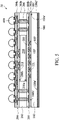
- FIG. 5 is a cross-sectional view of a semiconductor package structure 50 in accordance with some embodiments of the disclosure. Descriptions of elements of the embodiments hereinafter that are the same as or similar to those previously described with reference to FIG. 1 may be omitted for brevity.
- the semiconductor package structure 50 is similar to the semiconductor package structure 10 shown in FIG. 1 , except the first semiconductor die 100' and the first protective layer.
- the first semiconductor die 100' has a first surface 100a' and a second surface 100b' opposite thereto, and has different dimensions than the second semiconductor die 200.
- the second semiconductor die 200 has smaller dimensions than the first semiconductor die 100'.
- the first semiconductor die 100' may serve as a carrier substrate for the second semiconductor die 200.
- the first RDL structure 104 disposed on the first semiconductor die 100'does not serve as a fan-out layer for the first semiconductor die 100'.
- the first protective layer covers a sidewall 104a of the first RDL structure 104 and fills an opening 101' that is formed at the edge of the first semiconductor die 100', so as to cover a sidewall 100c' of opening 101'.
- the first protective layer serves as sidewall protection.
- the first protective layer is an extending portion 202a of the second molding compound 202. In this case, the extending portion 202a entirely covers the sidewall 104a of the first RDL structure 104 and partially exposes the sidewall 100d' of the first semiconductor die 100'.
- the bottom protective layer 500 disposed on the first surface 100a' of the first semiconductor die 100' via an adhesion layer 103' which is sometimes referred to as a DAF and is used for attaching the first semiconductor die 100' onto a carrier (not shown) during fabrication of the semiconductor package structure 50.
- the adhesion layer 103' has sidewalls that are substantially aligned with lower sidewalls of the first semiconductor die 100' and sidewalls of the bottom protective layer 500, so that the adhesion layer 103' and the bottom protective layer 500 substantially have the same width, as shown in FIG. 5 .
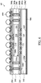
- FIG. 6 is a cross-sectional view of a semiconductor package structure 60 in accordance with some embodiments of the disclosure. Descriptions of elements of the embodiments hereinafter that are the same as or similar to those previously described with reference to FIGS. 1 and 5 may be omitted for brevity.
- the semiconductor package structure 60 is similar to the semiconductor package structure 50 shown in FIG. 5 except the first protective layer.
- the first protective layer covers a sidewall 104a of the first RDL structure 104 and the sidewall 100d' of the first semiconductor die 100'.
- the first protective layer serves as sidewall protection.
- the first protective layer is an extending portion 202a of the second molding compound 202. In this case, the extending portion 202a entirely covers the sidewalls 104a and 100d'.
- the first semiconductor die can serve as a carrier substrate for the overlying second semiconductor die, there is no need to form a molding compound to surround the first semiconductor die for supporting an overlying fan-out layer. As a result, the manufacturing cost can be reduced and the processes for the semiconductor package structure can be simplified.
Landscapes
- Structures Or Materials For Encapsulating Or Coating Semiconductor Devices Or Solid State Devices (AREA)
- Engineering & Computer Science (AREA)
- Manufacturing & Machinery (AREA)
- Microelectronics & Electronic Packaging (AREA)
Applications Claiming Priority (4)
| Application Number | Priority Date | Filing Date | Title |
|---|---|---|---|
| US201562237226P | 2015-10-05 | 2015-10-05 | |
| US201562237250P | 2015-10-05 | 2015-10-05 | |
| US15/218,379 US20170098629A1 (en) | 2015-10-05 | 2016-07-25 | Stacked fan-out package structure |
| EP16186728.8A EP3163614B1 (de) | 2015-10-05 | 2016-09-01 | Gestapelte ausfächerungspackungsstruktur |
Related Parent Applications (2)
| Application Number | Title | Priority Date | Filing Date |
|---|---|---|---|
| EP16186728.8A Division EP3163614B1 (de) | 2015-10-05 | 2016-09-01 | Gestapelte ausfächerungspackungsstruktur |
| EP16186728.8A Division-Into EP3163614B1 (de) | 2015-10-05 | 2016-09-01 | Gestapelte ausfächerungspackungsstruktur |
Publications (2)
| Publication Number | Publication Date |
|---|---|
| EP4006969A2 true EP4006969A2 (de) | 2022-06-01 |
| EP4006969A3 EP4006969A3 (de) | 2022-12-28 |
Family
ID=56853483
Family Applications (2)
| Application Number | Title | Priority Date | Filing Date |
|---|---|---|---|
| EP16186728.8A Active EP3163614B1 (de) | 2015-10-05 | 2016-09-01 | Gestapelte ausfächerungspackungsstruktur |
| EP22150096.0A Pending EP4006969A3 (de) | 2015-10-05 | 2016-09-01 | Gestapelte ausfächerungspackungsstruktur |
Family Applications Before (1)
| Application Number | Title | Priority Date | Filing Date |
|---|---|---|---|
| EP16186728.8A Active EP3163614B1 (de) | 2015-10-05 | 2016-09-01 | Gestapelte ausfächerungspackungsstruktur |
Country Status (4)
| Country | Link |
|---|---|
| US (2) | US20170098629A1 (de) |
| EP (2) | EP3163614B1 (de) |
| CN (1) | CN106653705B (de) |
| TW (1) | TWI702696B (de) |
Families Citing this family (31)
| Publication number | Priority date | Publication date | Assignee | Title |
|---|---|---|---|---|
| US9368460B2 (en) * | 2013-03-15 | 2016-06-14 | Taiwan Semiconductor Manufacturing Company, Ltd. | Fan-out interconnect structure and method for forming same |
| US20170098629A1 (en) * | 2015-10-05 | 2017-04-06 | Mediatek Inc. | Stacked fan-out package structure |
| US9825007B1 (en) * | 2016-07-13 | 2017-11-21 | Taiwan Semiconductor Manufacturing Co., Ltd. | Chip package structure with molding layer and method for forming the same |
| US11469215B2 (en) * | 2016-07-13 | 2022-10-11 | Taiwan Semiconductor Manufacturing Co., Ltd. | Chip package structure with molding layer and method for forming the same |
| US10304805B2 (en) | 2017-08-24 | 2019-05-28 | Micron Technology, Inc. | Dual sided fan-out package having low warpage across all temperatures |
| US10763239B2 (en) | 2017-10-27 | 2020-09-01 | Taiwan Semiconductor Manufacturing Co., Ltd. | Multi-chip wafer level packages and methods of forming the same |
| US11322449B2 (en) * | 2017-10-31 | 2022-05-03 | Taiwan Semiconductor Manufacturing Co., Ltd. | Package with fan-out structures |
| TWI647808B (zh) * | 2017-11-13 | 2019-01-11 | 旺宏電子股份有限公司 | 無銲墊外扇晶粒堆疊結構及其製作方法 |
| US10090232B1 (en) | 2017-11-13 | 2018-10-02 | Macronix International Co., Ltd. | Bumpless fan-out chip stacking structure and method for fabricating the same |
| KR102455427B1 (ko) | 2017-12-20 | 2022-10-17 | 삼성전자주식회사 | 반도체 패키지 및 이의 제조 방법 |
| US20200006274A1 (en) * | 2018-06-29 | 2020-01-02 | Powertech Technology Inc. | Semiconductor package and manufacturing method thereof |
| US10510591B1 (en) * | 2018-06-29 | 2019-12-17 | Taiwan Semiconductor Manufacturing Co., Ltd. | Package-on-package structure and method of manufacturing package |
| US10950554B2 (en) * | 2018-07-16 | 2021-03-16 | Taiwan Semiconductor Manufacturing Company, Ltd. | Semiconductor packages with electromagnetic interference shielding layer and methods of forming the same |
| KR102536269B1 (ko) * | 2018-09-14 | 2023-05-25 | 삼성전자주식회사 | 반도체 패키지 및 그 제조 방법 |
| CN111721989A (zh) * | 2019-03-22 | 2020-09-29 | 迈来芯电子科技有限公司 | 电流传感器 |
| US10818640B1 (en) * | 2019-04-02 | 2020-10-27 | Taiwan Semiconductor Manufacturing Company, Ltd. | Die stacks and methods forming same |
| US10777518B1 (en) * | 2019-05-16 | 2020-09-15 | Taiwan Semiconductor Manufacturing Co., Ltd. | Package structure and method of manufacturing the same |
| CN112133691A (zh) * | 2019-06-24 | 2020-12-25 | 台湾积体电路制造股份有限公司 | 半导体结构及其制作方法 |
| US11195816B2 (en) * | 2019-07-23 | 2021-12-07 | Taiwan Semiconductor Manufacturing Company, Ltd. | Integrated circuit packages comprising a plurality of redistribution structures and methods of forming the same |
| KR102424641B1 (ko) * | 2019-08-16 | 2022-07-25 | 타이완 세미콘덕터 매뉴팩쳐링 컴퍼니 리미티드 | 반도체 패키지 및 그 형성 방법 |
| US11322447B2 (en) * | 2019-08-16 | 2022-05-03 | Taiwan Semiconductor Manufacturing Company, Ltd. | Dual-sided routing in 3D SiP structure |
| DE102020106459B4 (de) * | 2019-08-30 | 2023-04-27 | Taiwan Semiconductor Manufacturing Co., Ltd. | Chip-package-struktur mit formungsschicht und verfahren zu deren bildung |
| CN112490129A (zh) * | 2019-09-11 | 2021-03-12 | 华邦电子股份有限公司 | 半导体封装及其制造方法 |
| US11824040B2 (en) * | 2019-09-27 | 2023-11-21 | Taiwan Semiconductor Manufacturing Company, Ltd. | Package component, electronic device and manufacturing method thereof |
| DE102020116106B4 (de) * | 2019-11-22 | 2023-11-09 | Taiwan Semiconductor Manufacturing Co., Ltd. | Halbleitervorrichtungen und herstellungsverfahren |
| KR102766435B1 (ko) * | 2020-02-17 | 2025-02-12 | 삼성전자주식회사 | 반도체 패키지 |
| US20210257335A1 (en) * | 2020-02-19 | 2021-08-19 | Nanya Technology Corporation | Semiconductor package and method of manufacturing the same |
| TWI815212B (zh) * | 2020-11-11 | 2023-09-11 | 南韓商Nepes股份有限公司 | 半導體封裝以及其製造方法 |
| TWI778654B (zh) * | 2021-06-09 | 2022-09-21 | 矽品精密工業股份有限公司 | 電子封裝件及其製法 |
| US12249566B1 (en) * | 2023-08-21 | 2025-03-11 | Taiwan Semiconductor Manufacturing Co., Ltd. | 3DIC with gap-fill structures and the method of manufacturing the same |
| CN117059586A (zh) * | 2023-08-31 | 2023-11-14 | 唯捷创芯(天津)电子技术股份有限公司 | 多层芯片封装结构及其制备方法 |
Citations (8)
| Publication number | Priority date | Publication date | Assignee | Title |
|---|---|---|---|---|
| US20070158857A1 (en) | 2006-01-10 | 2007-07-12 | Casio Computer Co., Ltd. | Semiconductor device having a plurality of semiconductor constructs |
| US20070262436A1 (en) | 2006-05-12 | 2007-11-15 | Micron Technology, Inc. | Microelectronic devices and methods for manufacturing microelectronic devices |
| WO2009009436A2 (en) | 2007-07-09 | 2009-01-15 | Micron Technology, Inc. | Packaged semiconductor assemblies and methods for manufacturing such assemblies |
| US7550857B1 (en) | 2006-11-16 | 2009-06-23 | Amkor Technology, Inc. | Stacked redistribution layer (RDL) die assembly package |
| US20110147911A1 (en) | 2009-12-22 | 2011-06-23 | Epic Technologies, Inc. | Stackable circuit structures and methods of fabrication thereof |
| US20140264817A1 (en) | 2013-03-13 | 2014-09-18 | Stats Chippac, Ltd. | Semiconductor Device and Method of Using Partial Wafer Singulation for Improved Wafer Level Embedded System in Package |
| WO2015138359A1 (en) | 2014-03-10 | 2015-09-17 | Deca Technologies Inc. | Semiconductor device and method comprising thickened redistribution layers |
| US20160148904A1 (en) | 2014-11-20 | 2016-05-26 | Apple Inc. | 3d integration of fanout wafer level packages |
Family Cites Families (23)
| Publication number | Priority date | Publication date | Assignee | Title |
|---|---|---|---|---|
| CN100350607C (zh) * | 2001-12-07 | 2007-11-21 | 富士通株式会社 | 半导体器件及其制造方法 |
| US8389867B2 (en) * | 2005-09-30 | 2013-03-05 | Ibiden Co., Ltd. | Multilayered circuit substrate with semiconductor device incorporated therein |
| KR20090007120A (ko) * | 2007-07-13 | 2009-01-16 | 삼성전자주식회사 | 봉지부를 통하여 재배선을 달성하는 웨이퍼 레벨 적층형패키지 및 그 제조방법 |
| US8383457B2 (en) * | 2010-09-03 | 2013-02-26 | Stats Chippac, Ltd. | Semiconductor device and method of forming interposer frame over semiconductor die to provide vertical interconnect |
| US8604600B2 (en) * | 2011-12-30 | 2013-12-10 | Deca Technologies Inc. | Fully molded fan-out |
| US20130040423A1 (en) * | 2011-08-10 | 2013-02-14 | Taiwan Semiconductor Manufacturing Company, Ltd. | Method of Multi-Chip Wafer Level Packaging |
| US9385006B2 (en) * | 2012-06-21 | 2016-07-05 | STATS ChipPAC Pte. Ltd. | Semiconductor device and method of forming an embedded SOP fan-out package |
| KR101985236B1 (ko) * | 2012-07-10 | 2019-06-03 | 삼성전자주식회사 | 멀티-칩 패키지 및 그의 제조 방법 |
| KR101429344B1 (ko) * | 2012-08-08 | 2014-08-12 | 앰코 테크놀로지 코리아 주식회사 | 반도체 패키지 및 그 제조 방법 |
| US9508674B2 (en) * | 2012-11-14 | 2016-11-29 | Taiwan Semiconductor Manufacturing Company, Ltd. | Warpage control of semiconductor die package |
| US9312198B2 (en) * | 2013-03-15 | 2016-04-12 | Intel Deutschland Gmbh | Chip package-in-package and method thereof |
| JP6259737B2 (ja) * | 2014-03-14 | 2018-01-10 | 東芝メモリ株式会社 | 半導体装置及びその製造方法 |
| US9601463B2 (en) * | 2014-04-17 | 2017-03-21 | Taiwan Semiconductor Manufacturing Company, Ltd. | Fan-out stacked system in package (SIP) and the methods of making the same |
| US20160013156A1 (en) * | 2014-07-14 | 2016-01-14 | Apple Inc. | Package-on-package options with multiple layer 3-d stacking |
| US9633974B2 (en) * | 2015-03-04 | 2017-04-25 | Apple Inc. | System in package fan out stacking architecture and process flow |
| US9786623B2 (en) * | 2015-03-17 | 2017-10-10 | STATS ChipPAC Pte. Ltd. | Semiconductor device and method of forming PoP semiconductor device with RDL over top package |
| US9659907B2 (en) * | 2015-04-07 | 2017-05-23 | Apple Inc. | Double side mounting memory integration in thin low warpage fanout package |
| US10068862B2 (en) * | 2015-04-09 | 2018-09-04 | STATS ChipPAC Pte. Ltd. | Semiconductor device and method of forming a package in-fan out package |
| US9666502B2 (en) * | 2015-04-17 | 2017-05-30 | Taiwan Semiconductor Manufacturing Company, Ltd. | Discrete polymer in fan-out packages |
| US9601471B2 (en) * | 2015-04-23 | 2017-03-21 | Apple Inc. | Three layer stack structure |
| US20160329299A1 (en) * | 2015-05-05 | 2016-11-10 | Mediatek Inc. | Fan-out package structure including antenna |
| US20170098629A1 (en) * | 2015-10-05 | 2017-04-06 | Mediatek Inc. | Stacked fan-out package structure |
| US9859245B1 (en) * | 2016-09-19 | 2018-01-02 | Taiwan Semiconductor Manufacturing Co., Ltd. | Chip package structure with bump and method for forming the same |
-
2016
- 2016-07-25 US US15/218,379 patent/US20170098629A1/en not_active Abandoned
- 2016-08-24 CN CN201610715257.4A patent/CN106653705B/zh active Active
- 2016-08-31 TW TW105128081A patent/TWI702696B/zh active
- 2016-09-01 EP EP16186728.8A patent/EP3163614B1/de active Active
- 2016-09-01 EP EP22150096.0A patent/EP4006969A3/de active Pending
-
2018
- 2018-05-01 US US15/968,449 patent/US10692789B2/en active Active
Patent Citations (8)
| Publication number | Priority date | Publication date | Assignee | Title |
|---|---|---|---|---|
| US20070158857A1 (en) | 2006-01-10 | 2007-07-12 | Casio Computer Co., Ltd. | Semiconductor device having a plurality of semiconductor constructs |
| US20070262436A1 (en) | 2006-05-12 | 2007-11-15 | Micron Technology, Inc. | Microelectronic devices and methods for manufacturing microelectronic devices |
| US7550857B1 (en) | 2006-11-16 | 2009-06-23 | Amkor Technology, Inc. | Stacked redistribution layer (RDL) die assembly package |
| WO2009009436A2 (en) | 2007-07-09 | 2009-01-15 | Micron Technology, Inc. | Packaged semiconductor assemblies and methods for manufacturing such assemblies |
| US20110147911A1 (en) | 2009-12-22 | 2011-06-23 | Epic Technologies, Inc. | Stackable circuit structures and methods of fabrication thereof |
| US20140264817A1 (en) | 2013-03-13 | 2014-09-18 | Stats Chippac, Ltd. | Semiconductor Device and Method of Using Partial Wafer Singulation for Improved Wafer Level Embedded System in Package |
| WO2015138359A1 (en) | 2014-03-10 | 2015-09-17 | Deca Technologies Inc. | Semiconductor device and method comprising thickened redistribution layers |
| US20160148904A1 (en) | 2014-11-20 | 2016-05-26 | Apple Inc. | 3d integration of fanout wafer level packages |
Also Published As
| Publication number | Publication date |
|---|---|
| TW201714264A (zh) | 2017-04-16 |
| US20180323127A1 (en) | 2018-11-08 |
| CN106653705A (zh) | 2017-05-10 |
| TWI702696B (zh) | 2020-08-21 |
| CN106653705B (zh) | 2020-01-03 |
| EP3163614A3 (de) | 2017-07-12 |
| US20170098629A1 (en) | 2017-04-06 |
| EP4006969A3 (de) | 2022-12-28 |
| EP3163614B1 (de) | 2022-03-16 |
| EP3163614A2 (de) | 2017-05-03 |
| US10692789B2 (en) | 2020-06-23 |
Similar Documents
| Publication | Publication Date | Title |
|---|---|---|
| EP3163614B1 (de) | Gestapelte ausfächerungspackungsstruktur | |
| US11631611B2 (en) | Wafer level chip scale packaging intermediate structure apparatus and method | |
| US11728292B2 (en) | Semiconductor package assembly having a conductive electromagnetic shield layer | |
| EP3154083B1 (de) | Fan-out package struktur mit eingebettetem umverdrahtungssubstrat | |
| EP3007225B1 (de) | Halbleitergehäuseanordnung | |
| US20230378078A1 (en) | Package with fan-out structures | |
| EP2996146B1 (de) | Halbleitergehäuseanordnung | |
| US10424563B2 (en) | Semiconductor package assembly and method for forming the same | |
| US10217724B2 (en) | Semiconductor package assembly with embedded IPD | |
| EP3951870A1 (de) | Verfahren zur herstellung einer fan-out-verpackungsstruktur | |
| US10515887B2 (en) | Fan-out package structure having stacked carrier substrates and method for forming the same | |
| US20160329299A1 (en) | Fan-out package structure including antenna | |
| TWI626717B (zh) | 半導體封裝結構 | |
| US10340198B2 (en) | Semiconductor package with embedded supporter and method for fabricating the same | |
| US12051616B2 (en) | Wafer level chip scale packaging intermediate structure apparatus and method | |
| TW201832328A (zh) | 半導體封裝結構 | |
| US20170141041A1 (en) | Semiconductor package assembly | |
| KR20130050077A (ko) | 스택 패키지 및 이의 제조 방법 |
Legal Events
| Date | Code | Title | Description |
|---|---|---|---|
| PUAI | Public reference made under article 153(3) epc to a published international application that has entered the european phase |
Free format text: ORIGINAL CODE: 0009012 |
|
| STAA | Information on the status of an ep patent application or granted ep patent |
Free format text: STATUS: THE APPLICATION HAS BEEN PUBLISHED |
|
| AC | Divisional application: reference to earlier application |
Ref document number: 3163614 Country of ref document: EP Kind code of ref document: P |
|
| AK | Designated contracting states |
Kind code of ref document: A2 Designated state(s): AL AT BE BG CH CY CZ DE DK EE ES FI FR GB GR HR HU IE IS IT LI LT LU LV MC MK MT NL NO PL PT RO RS SE SI SK SM TR |
|
| PUAL | Search report despatched |
Free format text: ORIGINAL CODE: 0009013 |
|
| AK | Designated contracting states |
Kind code of ref document: A3 Designated state(s): AL AT BE BG CH CY CZ DE DK EE ES FI FR GB GR HR HU IE IS IT LI LT LU LV MC MK MT NL NO PL PT RO RS SE SI SK SM TR |
|
| RIC1 | Information provided on ipc code assigned before grant |
Ipc: H01L 21/56 20060101ALN20221124BHEP Ipc: H01L 25/03 20060101ALI20221124BHEP Ipc: H01L 21/60 20060101ALI20221124BHEP Ipc: H01L 23/31 20060101ALI20221124BHEP Ipc: H01L 23/538 20060101AFI20221124BHEP |
|
| STAA | Information on the status of an ep patent application or granted ep patent |
Free format text: STATUS: REQUEST FOR EXAMINATION WAS MADE |
|
| 17P | Request for examination filed |
Effective date: 20230622 |
|
| RBV | Designated contracting states (corrected) |
Designated state(s): AL AT BE BG CH CY CZ DE DK EE ES FI FR GB GR HR HU IE IS IT LI LT LU LV MC MK MT NL NO PL PT RO RS SE SI SK SM TR |