EP4006907A1 - Verfahren zur bewertung der leistung einer schnittstellenschaltung und zugehörige vorrichtung - Google Patents
Verfahren zur bewertung der leistung einer schnittstellenschaltung und zugehörige vorrichtung Download PDFInfo
- Publication number
- EP4006907A1 EP4006907A1 EP21856927.5A EP21856927A EP4006907A1 EP 4006907 A1 EP4006907 A1 EP 4006907A1 EP 21856927 A EP21856927 A EP 21856927A EP 4006907 A1 EP4006907 A1 EP 4006907A1
- Authority
- EP
- European Patent Office
- Prior art keywords
- data
- reference voltage
- strobe
- signal receiver
- interface circuit
- Prior art date
- Legal status (The legal status is an assumption and is not a legal conclusion. Google has not performed a legal analysis and makes no representation as to the accuracy of the status listed.)
- Granted
Links
Images




Classifications
-
- G—PHYSICS
- G11—INFORMATION STORAGE
- G11C—STATIC STORES
- G11C29/00—Checking stores for correct operation ; Subsequent repair; Testing stores during standby or offline operation
- G11C29/02—Detection or location of defective auxiliary circuits, e.g. defective refresh counters
- G11C29/022—Detection or location of defective auxiliary circuits, e.g. defective refresh counters in I/O circuitry
-
- G—PHYSICS
- G11—INFORMATION STORAGE
- G11C—STATIC STORES
- G11C29/00—Checking stores for correct operation ; Subsequent repair; Testing stores during standby or offline operation
- G11C29/04—Detection or location of defective memory elements, e.g. cell constructio details, timing of test signals
- G11C29/08—Functional testing, e.g. testing during refresh, power-on self testing [POST] or distributed testing
- G11C29/12—Built-in arrangements for testing, e.g. built-in self testing [BIST] or interconnection details
- G11C29/46—Test trigger logic
-
- G—PHYSICS
- G11—INFORMATION STORAGE
- G11C—STATIC STORES
- G11C29/00—Checking stores for correct operation ; Subsequent repair; Testing stores during standby or offline operation
- G11C29/02—Detection or location of defective auxiliary circuits, e.g. defective refresh counters
- G11C29/023—Detection or location of defective auxiliary circuits, e.g. defective refresh counters in clock generator or timing circuitry
-
- G—PHYSICS
- G11—INFORMATION STORAGE
- G11C—STATIC STORES
- G11C29/00—Checking stores for correct operation ; Subsequent repair; Testing stores during standby or offline operation
- G11C29/02—Detection or location of defective auxiliary circuits, e.g. defective refresh counters
- G11C29/028—Detection or location of defective auxiliary circuits, e.g. defective refresh counters with adaption or trimming of parameters
-
- G—PHYSICS
- G11—INFORMATION STORAGE
- G11C—STATIC STORES
- G11C29/00—Checking stores for correct operation ; Subsequent repair; Testing stores during standby or offline operation
- G11C29/04—Detection or location of defective memory elements, e.g. cell constructio details, timing of test signals
- G11C29/08—Functional testing, e.g. testing during refresh, power-on self testing [POST] or distributed testing
- G11C29/12—Built-in arrangements for testing, e.g. built-in self testing [BIST] or interconnection details
- G11C29/12005—Built-in arrangements for testing, e.g. built-in self testing [BIST] or interconnection details comprising voltage or current generators
-
- G—PHYSICS
- G11—INFORMATION STORAGE
- G11C—STATIC STORES
- G11C29/00—Checking stores for correct operation ; Subsequent repair; Testing stores during standby or offline operation
- G11C29/04—Detection or location of defective memory elements, e.g. cell constructio details, timing of test signals
- G11C29/08—Functional testing, e.g. testing during refresh, power-on self testing [POST] or distributed testing
- G11C29/12—Built-in arrangements for testing, e.g. built-in self testing [BIST] or interconnection details
- G11C29/1201—Built-in arrangements for testing, e.g. built-in self testing [BIST] or interconnection details comprising I/O circuitry
-
- G—PHYSICS
- G11—INFORMATION STORAGE
- G11C—STATIC STORES
- G11C29/00—Checking stores for correct operation ; Subsequent repair; Testing stores during standby or offline operation
- G11C29/04—Detection or location of defective memory elements, e.g. cell constructio details, timing of test signals
- G11C29/08—Functional testing, e.g. testing during refresh, power-on self testing [POST] or distributed testing
- G11C29/12—Built-in arrangements for testing, e.g. built-in self testing [BIST] or interconnection details
- G11C29/12015—Built-in arrangements for testing, e.g. built-in self testing [BIST] or interconnection details comprising clock generation or timing circuitry
-
- G—PHYSICS
- G11—INFORMATION STORAGE
- G11C—STATIC STORES
- G11C29/00—Checking stores for correct operation ; Subsequent repair; Testing stores during standby or offline operation
- G11C29/04—Detection or location of defective memory elements, e.g. cell constructio details, timing of test signals
- G11C29/08—Functional testing, e.g. testing during refresh, power-on self testing [POST] or distributed testing
- G11C29/12—Built-in arrangements for testing, e.g. built-in self testing [BIST] or interconnection details
- G11C29/38—Response verification devices
-
- G—PHYSICS
- G11—INFORMATION STORAGE
- G11C—STATIC STORES
- G11C8/00—Arrangements for selecting an address in a digital store
- G11C8/18—Address timing or clocking circuits; Address control signal generation or management, e.g. for row address strobe [RAS] or column address strobe [CAS] signals
-
- G—PHYSICS
- G11—INFORMATION STORAGE
- G11C—STATIC STORES
- G11C29/00—Checking stores for correct operation ; Subsequent repair; Testing stores during standby or offline operation
- G11C29/04—Detection or location of defective memory elements, e.g. cell constructio details, timing of test signals
- G11C29/50—Marginal testing, e.g. race, voltage or current testing
- G11C2029/5004—Voltage
-
- G—PHYSICS
- G11—INFORMATION STORAGE
- G11C—STATIC STORES
- G11C2207/00—Indexing scheme relating to arrangements for writing information into, or reading information out from, a digital store
- G11C2207/22—Control and timing of internal memory operations
- G11C2207/2254—Calibration
-
- G—PHYSICS
- G11—INFORMATION STORAGE
- G11C—STATIC STORES
- G11C29/00—Checking stores for correct operation ; Subsequent repair; Testing stores during standby or offline operation
- G11C29/04—Detection or location of defective memory elements, e.g. cell constructio details, timing of test signals
- G11C29/50—Marginal testing, e.g. race, voltage or current testing
- G11C29/50012—Marginal testing, e.g. race, voltage or current testing of timing
-
- G—PHYSICS
- G11—INFORMATION STORAGE
- G11C—STATIC STORES
- G11C7/00—Arrangements for writing information into, or reading information out from, a digital store
- G11C7/04—Arrangements for writing information into, or reading information out from, a digital store with means for avoiding disturbances due to temperature effects
-
- G—PHYSICS
- G11—INFORMATION STORAGE
- G11C—STATIC STORES
- G11C7/00—Arrangements for writing information into, or reading information out from, a digital store
- G11C7/22—Read-write [R-W] timing or clocking circuits; Read-write [R-W] control signal generators or management
- G11C7/222—Clock generating, synchronizing or distributing circuits within memory device
Definitions
- the disclosure relates to the technical field of a semiconductor, and more specifically to a method for evaluating performance of an interface circuit, an apparatus for evaluating performance of an interface circuit, an electronic device, and a computer-readable storage medium.
- the semiconductor circuit may receive a data signal from a storage controller according to a data strobe signal provided from the storage controller.
- the received data signal can then be stored within the semiconductor memory.
- Performance of an interface circuit seriously influences data reception reliability, and therefore, it is needed to provide a reliable evaluation method for effectively evaluating the performance of the interface circuit of the semiconductor circuit.
- the disclosure relates to a method and apparatus for evaluating performance of an interface circuit, an electronic device, and a computer-readable storage medium.
- a method for evaluating performance of an interface circuit is provided.
- the interface circuit is configured to receive a data signal according to a data strobe signal.
- the method includes that: a reference voltage of the interface circuit is scanned to obtain each reference voltage; a sampling point of the data signal by the data strobe signal is scanned; a test result of the interface circuit under each reference voltage and each sampling point is obtained; and a data eye diagram is generated according to the test result.
- an apparatus for evaluating performance of an interface circuit is provided.
- the interface circuit is configured to receive a data signal according to a data strobe signal.
- the apparatus includes: a reference voltage scanning unit, configured to scan a reference voltage of the interface circuit to obtain each reference voltage; a sampling point scanning unit, configured to scan a sampling point of the data strobe signal to the data signal; a test result obtaining unit, configured to obtain a test result of the interface circuit under each reference voltage and each sampling point; and a data eye diagram generation unit, configured to generate a data eye diagram according to the test result.
- an electronic device including: at least one processor; and a storage device, configured to store at least one program.
- the at least one program is executed by the at least one processor, the at least one processor is enabled to implement the method of any embodiment provided by the disclosure.
- a computer-readable storage medium having a computer program stored thereon is provided.
- the program is executed by a processor, the method of any embodiment provided by the disclosure is implemented.
- the data eye diagram can thus be generated from these test results under each reference voltage and each sampling point, and the performance of the interface circuit can be effectively and reliably evaluated.
- the generated data eye diagram may also be utilized to quickly and accurately find the optimal target strobe-to-data time and/or target reference voltage of the interface circuit, so that the interface circuit may guarantee the accuracy of writing the data signal when receiving the data signal according to the data strobe signal.
- the block diagrams shown in the drawings are merely functional entities and do not necessarily have to correspond to physically independent entities. That is, the functional entities can be implemented in the form of software, or in at least one hardware module or integrated circuit, or in different networks and/or processor apparatuses and/or microcontroller apparatuses.
- FIG. 1 schematically shows a flow diagram of a method for evaluating performance of an interface circuit according to one embodiment of the disclosure.
- the interface circuit can be configured to receive a data signal DQ according to a data strobe signal (DQS or WCK).
- DQS data strobe signal
- the interface circuit can be the interface circuit of a semiconductor memory. In some embodiments, the interface circuit can be the interface circuit of the high-speed semiconductor memory. In some embodiments, the interface circuit can be the interface circuit of a mobile semiconductor memory.
- the disclosure does not make any limitation on it.
- the semiconductor memory can be any semiconductor memory, for example, a Double Data Rate Synchronous Dynamic Random-Access Memory (DDR SDRAM).
- DDR SDRAM Double Data Rate Synchronous Dynamic Random-Access Memory
- mark symbols adopted by the data strobe signal may vary, and the disclosure does not make any limitation on it.
- the method for evaluating performance of an interface circuit can include the following steps.
- a reference voltage of the interface circuit is scanned to obtain each reference voltage.
- the reference voltage of the interface circuit is scanned to obtain a plurality of reference voltages Vref.
- a sampling point of the data signal DQ by the data strobe signal (for example, DQS or WCK) is scanned.
- the data strobe signal can be represented as the DQS
- the following strobe-to-data time can be represented as tDQS2DQ
- the tDQS2DQ is the time difference tDQS2DQ between the data strobe signal DQS of the DDR4 or LPDDR4 and the data signal DQ.
- the semiconductor memory is DDR5/LPDDR5
- the following strobe-to-data time can be represented as tWCK2DQI
- the tWCK2DQI is the time difference tWCK2DQI between the data strobe signal WCK of the DDR5 or LPDDR5 and the data signal DQ.
- test result of the interface circuit under each reference voltage and each sampling point passes (represented by p) or fails (represented by X) is obtained.
- the data eye diagram can be generated.
- the method for evaluating performance of an interface circuit provided by the implementation mode of the disclosure, through scanning of each sampling point of the data strobe signal to the data signal and through combination of each reference voltage obtained by scanning the reference voltage of the interface circuit, the test result of the interface circuit under each reference voltage and each sampling point can be obtained, the data eye diagram can thus be generated from these test results under each reference voltage and each sampling point, and the performance of the interface circuit can be effectively and reliably evaluated.
- the generated data eye diagram may also be utilized to quickly and accurately find the optimal target strobe-to-data time and/or target reference voltage of the interface circuit, so that the interface circuit may guarantee the accuracy of writing the data signal when receiving the data signal according to the data strobe signal.
- the method provided by the embodiment of the disclosure can be used to simulate to generate the data eye diagrams with the same accuracy.
- FIG. 2 schematically shows a flow diagram of a method for evaluating performance of an interface circuit according to one embodiment of the disclosure.
- S110 in the above embodiment of FIG. 1 can include Sill.
- Sill a reference voltage range of the interface circuit is scanned with a second step size to obtain each reference voltage.
- the interface circuit has a corresponding reference voltage range, for example, the reference voltage Vref of the LPDDR4 is divided into two ranges (range [0]: VDDQ ranging from 10.0% to 30.0%, and range [1]: VDDQ ranging from 22.0% to 42.0%) as specified in a Joint Electron Device Engineering Council (JEDEC) standard.
- the step size of the two ranges is 0.4%.
- the two voltage reference ranges have an overlapping part, as shown in the following Table 1.
- V ref is set through a register OP [5:0] 000000 B :10.0 % 011010 B :20.4 % 000000 B :22.0 % 011010 B :32.4 % 000001 B :10.4 % 011011 B :20.8 % 000001 B :22.4 % 011011 B :32.8 % 000010 B :10.8 % 011100 B :21.2 % 000010 B :22.8 % 011100 B :33.2 % 000011 B :11.2 % 011101 B :21.6 % 000011 B :23.2 % 011101 B :33.6 % 000100 B :11.6 % 011110 B :22.0 % 000100 B :23.6 % 011110 B :34.0 % 000101 B :12.0 % 011111
- the second step size can include a third sub-step size and a fourth sub-step size.
- the third sub-step size is greater than the fourth sub-step size.
- the operation that a reference voltage range of the interface circuit is scanned in a second step size to obtain each reference voltage can include: an edge reference voltage range on at least one side of the reference voltage range is determined; the third sub-step size of the edge reference voltage range is set; a middle reference voltage range except for the edge reference voltage range in the reference voltage range is determined; the fourth sub-step size of the middle reference voltage range is set; and the edge reference voltage range is scanned with the third sub-step size, and the middle reference voltage range is scanned with the fourth sub-step size to obtain each reference voltage.
- each reference voltage Vref is taken as an ordinate value (second coordinate value)
- the reference voltage range at an upper side, or a lower side, or both the upper side and lower side of the reference voltage range can be taken as the edge reference voltage range
- the scanning is performed with the relatively great third sub-step size in the edge reference voltage range to obtain each reference voltage in the edge reference voltage range
- the scanning is performed with the relatively small fourth sub-step size in the middle reference voltage range except for the above edge reference voltage range to obtain each reference voltage in the middle reference voltage range.
- each reference voltage Vref is taken as an abscissa value (second coordinate value)
- the reference voltage range at a left side, or a right side, or both the left side and right side of the reference voltage range can be taken as the edge reference voltage range
- the scanning is performed with the relatively great third sub-step size in the edge reference voltage range to obtain each reference voltage in the edge reference voltage range
- the scanning is performed with the relatively small fourth sub-step size in the middle reference voltage range except for the above edge reference voltage range to obtain each reference voltage in the middle reference voltage range.
- the scanning is performed with the relatively great third sub-step size to obtain each reference voltage in the edge reference voltage range, so that the number of the finally obtained total reference voltages can be reduced, the occupied storage space is reduced, the computation amount is reduced, and the speed of obtaining a target reference voltage can be increased subsequently; and on the other hand, since the target reference voltage to be obtained subsequently through the data eye diagram is generally located in the middle of the reference voltage range, the scanning is performed with the relatively small fourth sub-step to obtain each reference voltage in the middle reference voltage range, the precision of the obtained target reference voltage can be improved.
- the scanning being performed with unequal step sizes (the third sub-step size and the fourth sub-step size) to obtain each reference voltage is taken as an example for illustration, the disclosure is not limited here. In other embodiments, the entire reference voltage range may also be scanned with an equal step size to obtain each reference voltage.
- S120 in the above embodiment of FIG. 1 can include S121.
- S121 a strobe-to-data time range of the interface circuit is scanned with a first step size to obtain each strobe-to-data time.
- the LPDDR4 is taken as an example, the strobe-to-data time is tDQS2DQ, and a tDQS2DQ range [T1, T2] can be [0 ps, 800 ps].
- the LPDDR5 is taken as an example, the strobe-to-data time is tWCK2DQI, and a tWCK2DQI range [T1, T2] can be [0 ps, 700 ps].
- the first step size can include a first sub-step size and a second sub-step size.
- the first sub-step size can be greater than the second sub-step size.
- the operation that a strobe-to-data time range of the interface circuit is scanned in a first step size to obtain each strobe-to-data time can include: an edge strobe-to-data time range on at least one side of the strobe-to-data time range is determined; the first sub-step size of the edge strobe-to-data time range is set; a middle strobe-to-data time range in the strobe-to-data time range except for the edge strobe-to-data time range is determined; the second sub-step size of the middle strobe-to-data time range is set; and the edge strobe-to-data time range is scanned with the first sub-step size, and the middle strobe-to-data time range is scanned with the second sub-step size, to obtain each strobe-to-data time.
- each strobe-to-data time is taken as an abscissa value (first coordinate value)
- the strobe-to-data time range at a left side, or a right side, or both the left side and right side of the strobe-to-data time range can be taken as the edge strobe-to-data time range
- the scanning is performed with the relatively great first sub-step size in the edge strobe-to-data time range to obtain each strobe-to-data time in the edge strobe-to-data time range
- the scanning is performed with the relatively small second sub-step size in the middle strobe-to-data time range except for the above edge strobe-to-data time range to obtain each strobe-to-data time in the middle strobe-to-data time range.
- each strobe-to-data time is taken as an ordinate value (first coordinate value)
- the strobe-to-data time range at an upper side, or a lower side, or both the upper side and lower side of the strobe-to-data time range can be taken as the edge strobe-to-data time range
- the scanning is performed with the relatively great first sub-step size in the edge strobe-to-data time range to obtain each strobe-to-data time in the edge strobe-to-data time range
- the scanning is performed with the relatively small second sub-step size in the middle strobe-to-data time range except for the above edge strobe-to-data time range to obtain each strobe-to-data time in the middle strobe-to-data time range.
- the scanning is performed with the relatively great first sub-step size to obtain each strobe-to-data time in the edge strobe-to-data time range, so that the number of the finally obtained total strobe-to-data time can be reduced, the occupied storage space is reduced, the computation amount is reduced, and the speed of obtaining target strobe-to-data time can be increased subsequently; and on the other hand, since the strobe-to-data time to be obtained subsequently through the data eye diagram is generally located in the middle of the strobe-to-data time range, the scanning is performed with the relatively small second sub-step to obtain each strobe-to-data time in the middle strobe-to-data time range, the precision of the obtained target strobe-to-data time can be improved.
- the scanning being performed with the unequal step sizes (the first sub-step size and the second sub-step size) to obtain each strobe-to-data time is taken as an example for illustration, the disclosure is not limited here. In other embodiments, the entire strobe-to-data time range may also be scanned with the equal step size to obtain each strobe-to-data time.
- the interface circuit can include a first signal receiver.
- one channel in the interface circuit can include 16 data signals (which can be respectively marked as DQ0 to DQ15, referred to as a first data signal to a sixteenth data signal)
- one byte group can include 8 data signals, for example, DQ0 to DQ7 in the same channel form one byte group, and DQ8 to DQ 15 form another byte group.
- the first signal receiver can be configured to receive the first data signal DQ0 in the data signals DQ, but the disclosure is not limited here.
- the first signal receiver can be configured to receive any data signal in the data signals DQ.
- the test result can include a first test result.
- the first signal receiver (which may also include a second signal receiver hereinafter) in the interface circuit may adopt the form of a single-ended signal.
- S130 in the above embodiment of FIG. 1 can include S131.
- S131 the first test result of the first signal receiver under each strobe-to-data time and each reference voltage is obtained.
- the operation that a data eye diagram is generated according to the test result can include: by taking each strobe-to-data time as a first coordinate value and taking each reference voltage as a second coordinate value, a two-dimensional data eye diagram displaying the test results is generated according to the test results under each strobe-to-data time and each reference voltage.
- S140 in the above embodiment of FIG. 1 can include S141.
- S141 by taking each strobe-to-data time as a first coordinate value and taking each reference voltage as a second coordinate value, the data eye diagram of the first signal receiver is generated according to the first test result of the first signal receiver.
- the first test result of the first signal receiver under each reference voltage and each strobe-to-data time is obtained to generate the data eye diagram of the first signal receiver. That is, according to the method provided by the embodiment of the disclosure, the data eye diagram of a single signal receiver can be obtained, the target strobe-to-data time and/or the target reference voltage of the single signal receiver can be located, meanwhile, an additional test bench is not needed, and the existing test bench is adopted.
- a test can be performed through the embodiment in FIG. 3 to obtain the first test result of the first signal receiver, but the disclosure is not limited here.
- FIG. 3 schematically shows a processing flow diagram of S131 in FIG. 2 in an example embodiment.
- the strobe-to-data time can include first strobe-to-data time
- the reference voltage can include a first reference voltage
- the interface circuit may further include a sampling signal terminal
- the data signal can include write-in data.
- the write-in data is received according to the sampling signal and the first reference voltage, and the write-in data is written into the target storage unit.
- the write-in data is compared with the read-out data to obtain the first test result of the first signal receiver under the first strobe-to-data time and the first reference voltage.
- the operation that the write-in data is compared with the read-out data to obtain the first test result of the first signal receiver under the first strobe-to-data time and the first reference voltage can include: if the write-in data is equal to the read-out data, the first test result of the first signal under the first strobe-to-data time and the first reference voltage passes; and if the write-in data is not equal to the read-out data, the first test result of the first signal receiver under the first strobe-to-data time and the first reference voltage fails.
- the embodiment may adapt to various test patterns, and a particular test pattern does not need to be specifically designed.
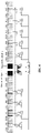
- FIG. 4 schematically shows a schematic diagram of a semiconductor memory according to one embodiment of the disclosure.
- the data strobe signal can include a data strobe signal_t and a data strobe signal c which are inverted signals.
- the LPDDR4 is taken as an example, the signal receiver corresponding to each data signal DQ is generally beside a DQ input port, and the data strobe signal DQS needs to be pulled from a data strobe signal DQS input port to the signal receiver corresponding to each DQ. Therefore, when performing a write operation, internal delay of the data strobe signal DQS in a receiving direction is greater than the internal delay of the data signal DQ, and such path mismatch may influence the accurate triggering of the write operation.
- the semiconductor memory requires a storage controller to compensate for delay difference between the data strobe signal DQS and the data signal DQ, and the data strobe signal DQS is sent earlier than the data signal DQ to ensure that the data strobe signal DQS and the data signal DQ can receive data accurately.
- Advanced sending time is defined in the JEDEC standard and is referred to as strobe-to-data time tDQS2DQ.
- the data strobe signal DQS in the LPDDR4 is taken as an example for illustration, and the data strobe signal can include DQS_t and DQS_c which are inverted.
- a correct timing problem of the strobe-to-data time tDQS2DQ is solved through the write operation.
- Each strobe-to-data time tDQS2DQ is determined first, and then the data strobe signal DQS is input into the LPDDR4. Then the data strobe signal DQS is respectively input to the signal receiver (for example, the first signal receiver to the fifteenth signal receiver) corresponding to each DQ (for example, the DQ0 to the DQ15 in FIG.
- the corresponding data signal DQ is respectively input to each signal receiver, and then the read-out data is obtained from the storage unit of the LPDDR4 corresponding to each signal receiver. Whether the write-in data and the read-out data of the corresponding signal receiver are consistent is compared, if so, the test result of the corresponding signal receiver passes, and if not, the test result of the corresponding signal receiver fails.
- VSSQ, VDDQ, and VDD2 in FIG. 4 respectively represent different power supply voltages in the semiconductor memory.
- DMI is an English abbreviation for Data Mask Inversion, that is, data mask inversion.
- the test can be performed after the packaging model and the channel model are added and this is more similar to an actual application scenario, so that the result is more accurate.
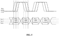
- FIG. 5 schematically shows a schematic diagram of a data strobe signal and a data valid window under different reference voltages according to one embodiment of the disclosure.
- the rising and falling edges of the data strobe signal for example, the DQS
- the rising and falling edges of the data strobe signal are preferably located just in the middle of a data valid window of a high-speed data signal, so that the high-speed data signal can be well captured.
- Vref1, Vref2, and Vref3 are taken as an example for illustration, assuming that rising and falling edges of the data strobe signal deviate from the middle of the data valid window under the Vref1 and Vref3 reference voltages. Under the Vref2 reference voltage, if the rising and falling edges of the data strobe signal are located just in the middle of the data valid window, the Vref2 can be taken as the target reference voltage.
- the method may further include: target strobe-to-data time and/or a target reference voltage is determined according to the data eye diagram.
- FIG. 6 schematically shows a schematic diagram of a data eye diagram according to one embodiment of the disclosure.
- the LPDDR4 is still taken as an example, assuming that the reference voltage Vref is taken as the ordinate value and the strobe-to-data time tDQS2DQ is taken as the abscissa value, the data eye diagram shown in FIG. 6 is generated according to pass (p) and fail (X) in the test result.
- the strobe-to-data time range can be scanned by adopting the same step size (for example, 20 ps) to obtain each strobe-to-data time
- the scanning may also be performed by adopting the relatively large first sub-step size in the edge strobe-to-data time range at the left side or the right side, or both the left side and the right side to obtain each strobe-to-data time in the edge strobe-to-data time range
- the scanning may also be performed by adopting the relatively small second sub-step in the middle strobe-to-data time range to obtain each strobe-to-data time in the middle strobe-to-data time range.
- the reference voltage range in FIG. 6 is [110 mV, 255 mV]
- the reference voltage range can be scanned by adopting the same step size to obtain each reference voltage
- the scanning may also be performed by adopting the relatively large third sub-step size in the edge reference voltage range at the upper side or the lower side, or both the upper side and the lower side to obtain each reference voltage in the edge reference voltage range
- the scanning may also be performed by adopting the relatively small fourth sub-step in the middle reference voltage range to obtain each reference voltage in the middle reference voltage range.
- the third sub-step size is equal to 25 mv and the fourth sub-step size is equal to 20 mv
- V0 110 mv
- V1 135 mv
- V2 155 mv
- V3 175 mv
- V4 195 mv
- V5 215 mv
- V6 235 mv
- V7 255 mv in FIG. 6 .
- the strobe-to-data time can be taken as the target strobe-to-data time.
- the interface circuit may further include the second signal receiver.
- the test result may further include a second test result.
- the second signal receiver can be any signal receiver.
- the second signal receiver can be the second signal receiver corresponding to the second data signal DQ1, but the disclosure is not limited here.
- the operation that a test result of the interface circuit under each reference voltage and each sampling point is obtained may further include: the second test result of the second signal receiver under each strobe-to-data time and each reference voltage is obtained.
- a procedure of obtaining the second test result may refer to the above description of obtaining the first test result.
- the operation that a data eye diagram is generated according to the test result may further include: by taking each strobe-to-data time as a first coordinate value and taking each reference voltage as a second coordinate value, the data eye diagram of the second signal receiver is generated according to the second test result of the second signal receiver.
- the mode of generating the data eye diagram of the second signal receiver may refer to the above mode of generating the data eye diagram of the first signal receiver.
- the method may further include: the data eye diagram of the first signal receiver is compared with the data eye diagram of the second signal receiver and offset between the first signal receiver and the second signal receiver is determined.
- the first signal receiver and the second signal receiver can be located in the same byte group.
- the first signal receiver and the second signal receiver are located in the same byte group (DQ0 to DQ7), but the disclosure is not limited here.
- the offset between any two adjacent DQs in the byte group can be obtained by comparing the data eye diagram of each DQ.
- FIG. 7 schematically shows a schematic diagram of a data eye diagram according to one embodiment of the disclosure.
- DQ0, DQ1, DQ2, and DQ3 in the byte group are taken as an example.
- the data eye diagram of each DQ can be independently displayed, so that the offset between the two adjacent DQs can be compared, and which DQ is problematic can be located, thereby modifying the design of the DQ.
- the method may further include: a composite eye diagram of the interface circuit is generated according to the data eye diagram of the first signal receiver and the data eye diagram of the second signal receiver.
- VDDQ 1.1 V.
- the data eye diagrams of 16 DQs (DQ0 to DQ15) as shown in FIG. 7 are obtained first, 'p' in each data eye diagram is represented by '1', and 'X' is represented by '0', and then the test results at corresponding positions of the 16 data eye diagrams are superposed to obtain the composite eye diagram of the interface circuit as shown in FIG. 8 . If a value at a certain position is 16, this represents that the test results of the DQ0 to DQ15 under the corresponding reference voltage and the corresponding strobe-to-data time pass.
- a value at a certain position 15 DQs in the DQ0 to DQ15 under the corresponding reference voltage and the corresponding strobe-to-data time pass, and the test result of one DQ fails. If a value at a certain position is 11, this represents that the test results of 11 DQs in the DQ0 to DQ15 under the corresponding reference voltage and the corresponding strobe-to-data time pass, and the test result of 5 DQ fail. If a value at a certain position is 6, this represents that the test results of 6 DQs in the DQ0 to DQ15 under the corresponding reference voltage and the corresponding strobe-to-data time pass, and the test result of 10 DQ fail.
- a value at a certain position is 4, this represents that the test results of 4 DQs in the DQ0 to DQ15 under the corresponding reference voltage and the corresponding strobe-to-data time pass, and the test result of 12 DQs fail. If a value at a certain position is 1, this represents that the test result of 1 DQ in the DQ0 to DQ15 under the corresponding reference voltage and the corresponding strobe-to-data time passes, and the test results of 15 DQs fail. If a value at a certain position is 0, this represents that the test results of 16 DQs in the DQ0 to DQ15 under the corresponding reference voltage and the corresponding strobe-to-data time fail.
- the center of the composite eye diagram can be taken as default target strobe-to-data time, and under the target strobe-to-data time, all DQ tests may pass. If the area of the zero-free region of the composite eye diagram is large, this represents that the performance of the interface circuit is better and the semiconductor memory can work normally in a relatively large fluctuation range.
- the operation that the data eye diagram of the first signal receiver is generated can include: the data eye diagram of the first signal receiver under a first process corner is obtained; and the data eye diagram of the first signal receiver under a second process corner is obtained.
- the method may further include: the composite eye diagram of the first signal receiver is generated according to the data eye diagram of the first signal receiver under the first process corner and the data eye diagram of the first signal receiver under the second process corner.
- the influence of different process corners on the interface circuit can be obtained by checking the composite eye diagrams under different process corners.
- the composite eye diagram of the interface circuit under the first process corner and the composite eye diagram of the interface circuit under the second process corner can be obtained.
- the performance of the interface circuit can be influenced by power, voltage, and temperature. Assuming that the first process corner is SS, a first power supply voltage is 1 V, and the first temperature is 85°C, the composite eye diagram of the interface circuit under the first process corner, the first power supply voltage, and the first temperature can be obtained.
- a second supply voltage is 1 V
- the second temperature is 25°C
- the composite eye diagram of the interface circuit under the second process corner, the second power supply voltage, and the second temperature can be obtained.
- a relationship between simulation and an actual test result of the chip of the semiconductor memory can be obtained, for example, some samples are manufactured, the samples are tested, the difference between the simulated test result and the test result of the sample is compared, an error between the simulation and the test result is eliminated, and the subsequently simulated test result is more accurate.
- An apparatus embodiment of the disclosure is described below and can be configured to execute the above method for evaluating performance of an interface circuit of the disclosure. For details not disclosed in the apparatus embodiment of the disclosure, reference is made to the embodiment of the above method for evaluating performance of an interface circuit of the disclosure.
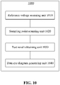
- FIG. 10 schematically shows a block diagram of an apparatus for evaluating performance of an interface circuit according to one embodiment of the disclosure.
- the interface circuit can be configured to receive a data signal according to a data strobe signal.
- the apparatus 1000 for evaluating performance of an interface circuit can include a reference voltage scanning unit 1010, a sampling point scanning unit 1020, a test result obtaining unit 1030, and a data eye diagram generating unit 1040.
- the reference voltage scanning unit 1010 can be configured to scan a reference voltage of the interface circuit to obtain each reference voltage.
- the sampling point scanning unit 1020 can be configured to scan a sampling point of the data strobe signal to the data signal.
- the test result obtaining unit 1030 can be configured to obtain a test result of the interface circuit under each reference voltage and each sampling point.
- the data eye diagram generating unit 1040 can be configured to generate a data eye diagram according to the test result.
- the sampling point scanning unit 1020 can include a strobe-to-data time obtaining unit which can be configured to scan a strobe-to-data time range of the interface circuit with a first step size to obtain each strobe-to-data time.
- the first step size can include a first sub-step size and a second sub-step size.
- the strobe-to-data time obtaining unit can include an edge strobe-to-data time range determining unit which can be configured to determine an edge strobe-to-data time range on at least one side of the strobe-to-data time range; a first sub-step size setting unit which can be configured to set the first sub-step size of the edge strobe-to-data time range; a middle strobe-to-data time range setting unit which can be configured to set a middle strobe-to-data time range in the strobe-to-data time range except for the edge strobe-to-data time range; a second sub-step size setting unit which can be configured to set the second sub-step size of the middle strobe-to-data time range; and a strobe-to-data time unit is obtained through scanning, which can be used in scanning the edge strobe-to-data time range with the first sub-step size, and the middle strobe-to-data time range can be scanned with the second sub-step size, to
- the first sub-step size can be greater than the second sub-step size.
- the reference voltage scanning unit 1010 can include a reference voltage obtaining unit, which can be configured to scan the reference voltage range of the interface circuit with a second step size, to obtain each reference voltage.
- the second step size can include a third sub-step size and a fourth sub-step size.
- the reference voltage obtaining unit can include: an edge reference voltage range determining unit, which can be configured to determine an edge reference voltage range on at least one side of the reference voltage range; a third sub-step size setting unit which can be configured to set the third sub-step size of the edge reference voltage range; a middle reference voltage range determining unit which can be configured to determine a middle reference voltage range except for the edge reference voltage range in the reference voltage range; a fourth sub-step size setting unit which can be configured to set the fourth sub-step size of the middle reference voltage range; and a reference voltage scan-to-obtain unit which can be configured to scan the edge reference voltage range with the third sub-step size, and scan the middle reference voltage range with the fourth sub-step size, to obtain each reference voltage.
- the third sub-step size can be greater than the fourth sub-step size.
- the data eye diagram generating unit 1040 can include: a two-dimensional data eye diagram generating unit which can be configured to, by taking each strobe-to-data time as a first coordinate value and taking each reference voltage as a second coordinate value, generate a two-dimensional data eye diagram displaying the test results according to the test results under each strobe-to-data time and each reference voltage.
- the interface circuit can include a first signal receiver.
- the test result can include a first test result.
- the test result obtaining unit 1030 can include: a first test result obtaining unit which can be configured to obtain the first test result of the first signal receiver under each strobe-to-data time and each reference voltage.
- the data eye diagram generating unit 1040 can include: a first signal receiver data eye diagram generating unit which can be configured to, by taking each strobe-to-data time as a first coordinate value and taking each reference voltage as a second coordinate value, generate the data eye diagram of the first signal receiver according to the first test result of the first signal receiver.
- the interface circuit may further include the second signal receiver.
- the test result may further include a second test result.
- the test result obtaining unit 1030 may further include: a second test result obtaining unit which can be configured to obtain the second test result of the second signal receiver under each strobe-to-data time and each reference voltage.
- the data eye diagram generating unit 1040 may further include: a second signal receiver data eye diagram generating unit which can be configured to, by taking each strobe-to-data time as a first coordinate value and taking each reference voltage as a second coordinate value, generate the data eye diagram of the second signal receiver according to the second test result of the second signal receiver.
- a second signal receiver data eye diagram generating unit which can be configured to, by taking each strobe-to-data time as a first coordinate value and taking each reference voltage as a second coordinate value, generate the data eye diagram of the second signal receiver according to the second test result of the second signal receiver.
- the apparatus 1000 for evaluating performance of an interface circuit may further include: an interface circuit composite eye diagram unit which can be configured to generate a composite eye diagram of the interface circuit according to the data eye diagram of the first signal receiver and the data eye diagram of the second signal receiver.
- the first signal receiver data eye diagram generating unit can include: a first process corner data eye diagram generating unit which can be configured to obtain the data eye diagram of the first signal receiver under a first process corner; and a second process corner data eye diagram generating unit which can be configured to obtain the data eye diagram of the first signal receiver under a second process corner.
- the apparatus 1000 for evaluating performance of an interface circuit may further include: a first signal receiver composite eye diagram generating unit which can be configured to generate the composite eye diagram of the first signal receiver according to the data eye diagram of the first signal receiver under the first process corner and the data eye diagram of the first signal receiver under the second process corner.
- a first signal receiver composite eye diagram generating unit which can be configured to generate the composite eye diagram of the first signal receiver according to the data eye diagram of the first signal receiver under the first process corner and the data eye diagram of the first signal receiver under the second process corner.
- the apparatus 1000 for evaluating performance of an interface circuit may further include: a data eye diagram comparing unit which can be configured to compare the data eye diagram of the first signal receiver with the data eye diagram of the second signal receiver and determine offset between the first signal receiver and the second signal receiver.
- a data eye diagram comparing unit which can be configured to compare the data eye diagram of the first signal receiver with the data eye diagram of the second signal receiver and determine offset between the first signal receiver and the second signal receiver.
- the first signal receiver and the second signal receiver can be located in the same byte group.
- the first signal receiver may correspond to a target storage unit in a semiconductor memory
- the strobe-to-data time can include first strobe-to-data time
- the reference voltage can include a first reference voltage
- the interface circuit may further include a sampling signal terminal
- the data signal can include write-in data.
- the first test result obtaining unit can include: a sampling signal sending unit which can be configured to send a sampling signal to the sampling signal terminal; a write-in data sending unit which can be configured to, after delaying the first strobe-to-data time, send write-in data to the first signal receiver; a write-in data write-in unit which can be configured to receive the write-in data according to the sampling signal and the first reference voltage and write the write-in data into the target storage unit; a read-out data obtaining unit which can be configured to obtain read-out data from the target storage unit; and a first test result obtaining unit which can be configured to compare the write-in data with the read-out data to obtain the first test result of the first signal receiver under the first strobe-to-data time and the first reference voltage.
- the first test result obtaining unit can include: a first comparing unit which can be configured to, if the write-in data is equal to the read-out data, indicate that the first test result of the first signal under the first strobe-to-data time and the first reference voltage passes; and a second comparing unit which can be configured to, if the write-in data is not equal to the read-out data, indicate that the first test result of the first signal receiver under the first strobe-to-data time and the first reference voltage fails.
- the apparatus 1000 for evaluating performance of an interface circuit may further include: a target strobe-to-data time determining unit and/or a target reference voltage determining unit.
- the target strobe-to-data time determining unit can be configured to determine target strobe-to-data time according to the data eye diagram.
- the target reference voltage determining unit can be configured to determine a target reference voltage according to the data eye diagram.
- the example implementation mode described here can be implemented through software or may also be implemented through the software in combination with necessary hardware. Therefore, the technical solution according to the embodiment of the disclosure can be embodied in the form of a software product.
- the software product can be stored in a non-volatile storage medium (which can be a CD-ROM, a U-disk, a mobile hard disk, and the like) or on a network, and can include a number of instructions, so that a computing device (which can be a personal computer, a server, a touch terminal, or a network device, and the like) executes the method according to the embodiment of the disclosure.
- an implementation mode of the disclosure further provides an electronic device, including: at least one processor; and a storage device, configured to store at least one program.
- the at least one program is executed by the at least one processor, the at least one processor is enabled to implement the method in any above embodiment.
- an implementation mode of the disclosure further provides a computer-readable storage medium having a computer program stored thereon.
- the program is executed by a processor, the method in any above embodiment provided by the disclosure is implemented.
Landscapes
- Engineering & Computer Science (AREA)
- Microelectronics & Electronic Packaging (AREA)
- Tests Of Electronic Circuits (AREA)
Applications Claiming Priority (2)
| Application Number | Priority Date | Filing Date | Title |
|---|---|---|---|
| CN202011015986.1A CN114255819B (zh) | 2020-09-24 | 2020-09-24 | 接口电路性能的评估方法及相关设备 |
| PCT/CN2021/101335 WO2022062504A1 (zh) | 2020-09-24 | 2021-06-21 | 接口电路性能的评估方法及相关设备 |
Publications (3)
| Publication Number | Publication Date |
|---|---|
| EP4006907A1 true EP4006907A1 (de) | 2022-06-01 |
| EP4006907A4 EP4006907A4 (de) | 2022-11-16 |
| EP4006907B1 EP4006907B1 (de) | 2024-02-07 |
Family
ID=80739387
Family Applications (1)
| Application Number | Title | Priority Date | Filing Date |
|---|---|---|---|
| EP21856927.5A Active EP4006907B1 (de) | 2020-09-24 | 2021-06-21 | Verfahren zur bewertung der leistung einer schnittstellenschaltung und zugehörige vorrichtung |
Country Status (2)
| Country | Link |
|---|---|
| US (1) | US20220093205A1 (de) |
| EP (1) | EP4006907B1 (de) |
Families Citing this family (5)
| Publication number | Priority date | Publication date | Assignee | Title |
|---|---|---|---|---|
| TWI806516B (zh) * | 2022-03-24 | 2023-06-21 | 瑞昱半導體股份有限公司 | 記憶體控制器與校準資料接收視窗的方法 |
| CN114822634B (zh) * | 2022-04-20 | 2025-09-16 | 芯来智融半导体科技(上海)有限公司 | 参考电压确定方法、装置、计算机设备和存储介质 |
| CN116013401B (zh) * | 2023-03-24 | 2023-08-11 | 长鑫存储技术有限公司 | 存储器调试方法、装置、设备及存储介质 |
| CN117250566B (zh) * | 2023-09-18 | 2024-05-03 | 珠海智融科技股份有限公司 | Type-C连接检测电路及电子设备 |
| CN119274632A (zh) * | 2024-12-10 | 2025-01-07 | 上海壁仞科技股份有限公司 | 数字眼图测试方法、装置、电子设备和存储介质 |
Family Cites Families (12)
| Publication number | Priority date | Publication date | Assignee | Title |
|---|---|---|---|---|
| US7036053B2 (en) * | 2002-12-19 | 2006-04-25 | Intel Corporation | Two dimensional data eye centering for source synchronous data transfers |
| DE102009004565B4 (de) * | 2009-01-14 | 2015-04-02 | Texas Instruments Deutschland Gmbh | Vorrichtung und Verfahren zum Zwischenspeichern von Daten zwischen Speichercontroller und DRAM |
| US7957218B2 (en) * | 2009-06-11 | 2011-06-07 | Freescale Semiconductor, Inc. | Memory controller with skew control and method |
| US8588014B1 (en) * | 2011-05-31 | 2013-11-19 | Altera Corporation | Methods for memory interface calibration |
| TWI550631B (zh) * | 2014-08-04 | 2016-09-21 | 瑞昱半導體股份有限公司 | 記憶體控制電路及相關的記憶體控制方法 |
| US9558850B1 (en) * | 2015-12-01 | 2017-01-31 | International Business Machines Corporation | Efficient calibration of a data eye for memory devices |
| US9620184B1 (en) * | 2015-12-16 | 2017-04-11 | International Business Machines Corporation | Efficient calibration of memory devices |
| US9715907B1 (en) * | 2016-05-09 | 2017-07-25 | Invecas, Inc. | Optimal data eye for improved Vref margin |
| US10566037B1 (en) * | 2018-07-27 | 2020-02-18 | Western Digital Technologies, Inc | Automated voltage and timing margin measurement for NAND flash interface |
| KR102679157B1 (ko) * | 2018-10-30 | 2024-06-27 | 삼성전자주식회사 | 모드 레지스터 쓰기 명령을 이용하여 쓰기 클럭의 듀티 사이클의 트레이닝을 수행하는 시스템 온 칩, 시스템 온 칩의 동작 방법, 및 시스템 온 칩을 포함하는 전자 장치 |
| CN110223722B (zh) * | 2019-07-05 | 2021-04-27 | 晶晨半导体(上海)股份有限公司 | 获取数据接口门限电压的方法及系统 |
| CN110928731B (zh) * | 2019-10-14 | 2024-05-14 | 珠海亿智电子科技有限公司 | 一种基于硬件自测模块的dram眼图评估方法 |
-
2021
- 2021-06-21 EP EP21856927.5A patent/EP4006907B1/de active Active
- 2021-08-22 US US17/445,605 patent/US20220093205A1/en not_active Abandoned
Also Published As
| Publication number | Publication date |
|---|---|
| EP4006907A4 (de) | 2022-11-16 |
| US20220093205A1 (en) | 2022-03-24 |
| EP4006907B1 (de) | 2024-02-07 |
Similar Documents
| Publication | Publication Date | Title |
|---|---|---|
| EP4006907B1 (de) | Verfahren zur bewertung der leistung einer schnittstellenschaltung und zugehörige vorrichtung | |
| CN114255819B (zh) | 接口电路性能的评估方法及相关设备 | |
| US7421558B2 (en) | System controlling interface timing in memory module and related method | |
| US7622908B2 (en) | Built-in system and method for testing integrated circuit timing parameters | |
| US20070277066A1 (en) | System and method for more efficiently using error correction codes to facilitate memory device testing | |
| CN115640172B (zh) | 电路仿真测试方法、装置、设备及介质 | |
| US9043518B2 (en) | Method and apparatus for calibrating a memory interface with a number of data patterns | |
| US20100082967A1 (en) | Method for detecting memory training result and computer system using such method | |
| US9477259B2 (en) | Calibration of clock signal for data transmission | |
| CN108009372B (zh) | 一种ddr内存虚拟写电平校准响应的方法 | |
| US20010000820A1 (en) | Method and apparatus for detecting an initialization signal and a command packet error in packetized dynamic random access memories | |
| US9323538B1 (en) | Systems and methods for memory interface calibration | |
| US11145343B1 (en) | Method for controlling multi-cycle write leveling process in memory system | |
| EP4390938A1 (de) | Speichervorrichtung und datentrainingsverfahren dafür | |
| US8122320B2 (en) | Integrated circuit including an ECC error counter | |
| US20030182611A1 (en) | Method for verifying error correction code function of a computer system | |
| US7710792B2 (en) | Semiconductor device | |
| KR100736675B1 (ko) | 반도체 소자 테스트 장치 | |
| US12339699B2 (en) | Memory, control apparatus, clock processing method, and electronic device | |
| US8370568B2 (en) | Memory interface and adaptive data access method | |
| US11545200B1 (en) | Data control circuit for increasing maximum and minimum tolerance values of skew between DQS signal and clock signal during write operation and associated memory device | |
| US20200066316A1 (en) | Memory circuit and method thereof | |
| US11906583B2 (en) | Method and measurement instrument for testing a device under test | |
| US12505014B1 (en) | DRAM ECC circuit error detection integrity | |
| US7668027B2 (en) | Semiconductor device, testing and manufacturing methods thereof |
Legal Events
| Date | Code | Title | Description |
|---|---|---|---|
| STAA | Information on the status of an ep patent application or granted ep patent |
Free format text: STATUS: UNKNOWN |
|
| STAA | Information on the status of an ep patent application or granted ep patent |
Free format text: STATUS: THE INTERNATIONAL PUBLICATION HAS BEEN MADE |
|
| PUAI | Public reference made under article 153(3) epc to a published international application that has entered the european phase |
Free format text: ORIGINAL CODE: 0009012 |
|
| STAA | Information on the status of an ep patent application or granted ep patent |
Free format text: STATUS: REQUEST FOR EXAMINATION WAS MADE |
|
| 17P | Request for examination filed |
Effective date: 20220222 |
|
| AK | Designated contracting states |
Kind code of ref document: A1 Designated state(s): AL AT BE BG CH CY CZ DE DK EE ES FI FR GB GR HR HU IE IS IT LI LT LU LV MC MK MT NL NO PL PT RO RS SE SI SK SM TR |
|
| A4 | Supplementary search report drawn up and despatched |
Effective date: 20221017 |
|
| RIC1 | Information provided on ipc code assigned before grant |
Ipc: G11C 29/50 20060101ALN20221011BHEP Ipc: G11C 7/22 20060101ALN20221011BHEP Ipc: G11C 7/04 20060101ALN20221011BHEP Ipc: G11C 29/12 20060101ALI20221011BHEP Ipc: G11C 29/02 20060101AFI20221011BHEP |
|
| REG | Reference to a national code |
Ref country code: DE Ref legal event code: R079 Free format text: PREVIOUS MAIN CLASS: G11C0029360000 Ipc: G11C0029020000 Ref country code: DE Ref legal event code: R079 Ref document number: 602021009259 Country of ref document: DE Free format text: PREVIOUS MAIN CLASS: G11C0029360000 Ipc: G11C0029020000 |
|
| GRAP | Despatch of communication of intention to grant a patent |
Free format text: ORIGINAL CODE: EPIDOSNIGR1 |
|
| STAA | Information on the status of an ep patent application or granted ep patent |
Free format text: STATUS: GRANT OF PATENT IS INTENDED |
|
| RIC1 | Information provided on ipc code assigned before grant |
Ipc: G11C 29/50 20060101ALN20230428BHEP Ipc: G11C 7/22 20060101ALN20230428BHEP Ipc: G11C 7/04 20060101ALN20230428BHEP Ipc: G11C 29/12 20060101ALI20230428BHEP Ipc: G11C 29/02 20060101AFI20230428BHEP |
|
| DAV | Request for validation of the european patent (deleted) | ||
| DAX | Request for extension of the european patent (deleted) | ||
| INTG | Intention to grant announced |
Effective date: 20230524 |
|
| RIN1 | Information on inventor provided before grant (corrected) |
Inventor name: WU, ZENGQUAN Inventor name: LIN, FENG |
|
| GRAJ | Information related to disapproval of communication of intention to grant by the applicant or resumption of examination proceedings by the epo deleted |
Free format text: ORIGINAL CODE: EPIDOSDIGR1 |
|
| STAA | Information on the status of an ep patent application or granted ep patent |
Free format text: STATUS: REQUEST FOR EXAMINATION WAS MADE |
|
| P01 | Opt-out of the competence of the unified patent court (upc) registered |
Effective date: 20230822 |
|
| GRAP | Despatch of communication of intention to grant a patent |
Free format text: ORIGINAL CODE: EPIDOSNIGR1 |
|
| STAA | Information on the status of an ep patent application or granted ep patent |
Free format text: STATUS: GRANT OF PATENT IS INTENDED |
|
| INTC | Intention to grant announced (deleted) | ||
| RIC1 | Information provided on ipc code assigned before grant |
Ipc: G11C 29/50 20060101ALN20230907BHEP Ipc: G11C 7/22 20060101ALN20230907BHEP Ipc: G11C 7/04 20060101ALN20230907BHEP Ipc: G11C 29/12 20060101ALI20230907BHEP Ipc: G11C 29/02 20060101AFI20230907BHEP |
|
| INTG | Intention to grant announced |
Effective date: 20231010 |
|
| GRAS | Grant fee paid |
Free format text: ORIGINAL CODE: EPIDOSNIGR3 |
|
| GRAA | (expected) grant |
Free format text: ORIGINAL CODE: 0009210 |
|
| STAA | Information on the status of an ep patent application or granted ep patent |
Free format text: STATUS: THE PATENT HAS BEEN GRANTED |
|
| AK | Designated contracting states |
Kind code of ref document: B1 Designated state(s): AL AT BE BG CH CY CZ DE DK EE ES FI FR GB GR HR HU IE IS IT LI LT LU LV MC MK MT NL NO PL PT RO RS SE SI SK SM TR |
|
| REG | Reference to a national code |
Ref country code: GB Ref legal event code: FG4D |
|
| REG | Reference to a national code |
Ref country code: CH Ref legal event code: EP |
|
| REG | Reference to a national code |
Ref country code: DE Ref legal event code: R096 Ref document number: 602021009259 Country of ref document: DE |
|
| REG | Reference to a national code |
Ref country code: IE Ref legal event code: FG4D |
|
| REG | Reference to a national code |
Ref country code: LT Ref legal event code: MG9D |
|
| REG | Reference to a national code |
Ref country code: NL Ref legal event code: MP Effective date: 20240207 |
|
| PG25 | Lapsed in a contracting state [announced via postgrant information from national office to epo] |
Ref country code: IS Free format text: LAPSE BECAUSE OF FAILURE TO SUBMIT A TRANSLATION OF THE DESCRIPTION OR TO PAY THE FEE WITHIN THE PRESCRIBED TIME-LIMIT Effective date: 20240607 |
|
| PG25 | Lapsed in a contracting state [announced via postgrant information from national office to epo] |
Ref country code: LT Free format text: LAPSE BECAUSE OF FAILURE TO SUBMIT A TRANSLATION OF THE DESCRIPTION OR TO PAY THE FEE WITHIN THE PRESCRIBED TIME-LIMIT Effective date: 20240207 |
|
| PG25 | Lapsed in a contracting state [announced via postgrant information from national office to epo] |
Ref country code: GR Free format text: LAPSE BECAUSE OF FAILURE TO SUBMIT A TRANSLATION OF THE DESCRIPTION OR TO PAY THE FEE WITHIN THE PRESCRIBED TIME-LIMIT Effective date: 20240508 |
|
| REG | Reference to a national code |
Ref country code: AT Ref legal event code: MK05 Ref document number: 1655883 Country of ref document: AT Kind code of ref document: T Effective date: 20240207 |
|
| PG25 | Lapsed in a contracting state [announced via postgrant information from national office to epo] |
Ref country code: NL Free format text: LAPSE BECAUSE OF FAILURE TO SUBMIT A TRANSLATION OF THE DESCRIPTION OR TO PAY THE FEE WITHIN THE PRESCRIBED TIME-LIMIT Effective date: 20240207 Ref country code: HR Free format text: LAPSE BECAUSE OF FAILURE TO SUBMIT A TRANSLATION OF THE DESCRIPTION OR TO PAY THE FEE WITHIN THE PRESCRIBED TIME-LIMIT Effective date: 20240207 Ref country code: RS Free format text: LAPSE BECAUSE OF FAILURE TO SUBMIT A TRANSLATION OF THE DESCRIPTION OR TO PAY THE FEE WITHIN THE PRESCRIBED TIME-LIMIT Effective date: 20240507 |
|
| PG25 | Lapsed in a contracting state [announced via postgrant information from national office to epo] |
Ref country code: ES Free format text: LAPSE BECAUSE OF FAILURE TO SUBMIT A TRANSLATION OF THE DESCRIPTION OR TO PAY THE FEE WITHIN THE PRESCRIBED TIME-LIMIT Effective date: 20240207 |
|
| PG25 | Lapsed in a contracting state [announced via postgrant information from national office to epo] |
Ref country code: AT Free format text: LAPSE BECAUSE OF FAILURE TO SUBMIT A TRANSLATION OF THE DESCRIPTION OR TO PAY THE FEE WITHIN THE PRESCRIBED TIME-LIMIT Effective date: 20240207 |
|
| PG25 | Lapsed in a contracting state [announced via postgrant information from national office to epo] |
Ref country code: RS Free format text: LAPSE BECAUSE OF FAILURE TO SUBMIT A TRANSLATION OF THE DESCRIPTION OR TO PAY THE FEE WITHIN THE PRESCRIBED TIME-LIMIT Effective date: 20240507 Ref country code: NO Free format text: LAPSE BECAUSE OF FAILURE TO SUBMIT A TRANSLATION OF THE DESCRIPTION OR TO PAY THE FEE WITHIN THE PRESCRIBED TIME-LIMIT Effective date: 20240507 Ref country code: NL Free format text: LAPSE BECAUSE OF FAILURE TO SUBMIT A TRANSLATION OF THE DESCRIPTION OR TO PAY THE FEE WITHIN THE PRESCRIBED TIME-LIMIT Effective date: 20240207 Ref country code: LT Free format text: LAPSE BECAUSE OF FAILURE TO SUBMIT A TRANSLATION OF THE DESCRIPTION OR TO PAY THE FEE WITHIN THE PRESCRIBED TIME-LIMIT Effective date: 20240207 Ref country code: IS Free format text: LAPSE BECAUSE OF FAILURE TO SUBMIT A TRANSLATION OF THE DESCRIPTION OR TO PAY THE FEE WITHIN THE PRESCRIBED TIME-LIMIT Effective date: 20240607 Ref country code: HR Free format text: LAPSE BECAUSE OF FAILURE TO SUBMIT A TRANSLATION OF THE DESCRIPTION OR TO PAY THE FEE WITHIN THE PRESCRIBED TIME-LIMIT Effective date: 20240207 Ref country code: GR Free format text: LAPSE BECAUSE OF FAILURE TO SUBMIT A TRANSLATION OF THE DESCRIPTION OR TO PAY THE FEE WITHIN THE PRESCRIBED TIME-LIMIT Effective date: 20240508 Ref country code: FI Free format text: LAPSE BECAUSE OF FAILURE TO SUBMIT A TRANSLATION OF THE DESCRIPTION OR TO PAY THE FEE WITHIN THE PRESCRIBED TIME-LIMIT Effective date: 20240207 Ref country code: ES Free format text: LAPSE BECAUSE OF FAILURE TO SUBMIT A TRANSLATION OF THE DESCRIPTION OR TO PAY THE FEE WITHIN THE PRESCRIBED TIME-LIMIT Effective date: 20240207 Ref country code: BG Free format text: LAPSE BECAUSE OF FAILURE TO SUBMIT A TRANSLATION OF THE DESCRIPTION OR TO PAY THE FEE WITHIN THE PRESCRIBED TIME-LIMIT Effective date: 20240207 Ref country code: AT Free format text: LAPSE BECAUSE OF FAILURE TO SUBMIT A TRANSLATION OF THE DESCRIPTION OR TO PAY THE FEE WITHIN THE PRESCRIBED TIME-LIMIT Effective date: 20240207 |
|
| PG25 | Lapsed in a contracting state [announced via postgrant information from national office to epo] |
Ref country code: PL Free format text: LAPSE BECAUSE OF FAILURE TO SUBMIT A TRANSLATION OF THE DESCRIPTION OR TO PAY THE FEE WITHIN THE PRESCRIBED TIME-LIMIT Effective date: 20240207 Ref country code: PT Free format text: LAPSE BECAUSE OF FAILURE TO SUBMIT A TRANSLATION OF THE DESCRIPTION OR TO PAY THE FEE WITHIN THE PRESCRIBED TIME-LIMIT Effective date: 20240607 |
|
| PG25 | Lapsed in a contracting state [announced via postgrant information from national office to epo] |
Ref country code: SE Free format text: LAPSE BECAUSE OF FAILURE TO SUBMIT A TRANSLATION OF THE DESCRIPTION OR TO PAY THE FEE WITHIN THE PRESCRIBED TIME-LIMIT Effective date: 20240207 Ref country code: PT Free format text: LAPSE BECAUSE OF FAILURE TO SUBMIT A TRANSLATION OF THE DESCRIPTION OR TO PAY THE FEE WITHIN THE PRESCRIBED TIME-LIMIT Effective date: 20240607 Ref country code: PL Free format text: LAPSE BECAUSE OF FAILURE TO SUBMIT A TRANSLATION OF THE DESCRIPTION OR TO PAY THE FEE WITHIN THE PRESCRIBED TIME-LIMIT Effective date: 20240207 Ref country code: LV Free format text: LAPSE BECAUSE OF FAILURE TO SUBMIT A TRANSLATION OF THE DESCRIPTION OR TO PAY THE FEE WITHIN THE PRESCRIBED TIME-LIMIT Effective date: 20240207 |
|
| PG25 | Lapsed in a contracting state [announced via postgrant information from national office to epo] |
Ref country code: DK Free format text: LAPSE BECAUSE OF FAILURE TO SUBMIT A TRANSLATION OF THE DESCRIPTION OR TO PAY THE FEE WITHIN THE PRESCRIBED TIME-LIMIT Effective date: 20240207 |
|
| PG25 | Lapsed in a contracting state [announced via postgrant information from national office to epo] |
Ref country code: SM Free format text: LAPSE BECAUSE OF FAILURE TO SUBMIT A TRANSLATION OF THE DESCRIPTION OR TO PAY THE FEE WITHIN THE PRESCRIBED TIME-LIMIT Effective date: 20240207 |
|
| PG25 | Lapsed in a contracting state [announced via postgrant information from national office to epo] |
Ref country code: CZ Free format text: LAPSE BECAUSE OF FAILURE TO SUBMIT A TRANSLATION OF THE DESCRIPTION OR TO PAY THE FEE WITHIN THE PRESCRIBED TIME-LIMIT Effective date: 20240207 Ref country code: EE Free format text: LAPSE BECAUSE OF FAILURE TO SUBMIT A TRANSLATION OF THE DESCRIPTION OR TO PAY THE FEE WITHIN THE PRESCRIBED TIME-LIMIT Effective date: 20240207 |
|
| PG25 | Lapsed in a contracting state [announced via postgrant information from national office to epo] |
Ref country code: SK Free format text: LAPSE BECAUSE OF FAILURE TO SUBMIT A TRANSLATION OF THE DESCRIPTION OR TO PAY THE FEE WITHIN THE PRESCRIBED TIME-LIMIT Effective date: 20240207 |
|
| PG25 | Lapsed in a contracting state [announced via postgrant information from national office to epo] |
Ref country code: SM Free format text: LAPSE BECAUSE OF FAILURE TO SUBMIT A TRANSLATION OF THE DESCRIPTION OR TO PAY THE FEE WITHIN THE PRESCRIBED TIME-LIMIT Effective date: 20240207 Ref country code: SK Free format text: LAPSE BECAUSE OF FAILURE TO SUBMIT A TRANSLATION OF THE DESCRIPTION OR TO PAY THE FEE WITHIN THE PRESCRIBED TIME-LIMIT Effective date: 20240207 Ref country code: RO Free format text: LAPSE BECAUSE OF FAILURE TO SUBMIT A TRANSLATION OF THE DESCRIPTION OR TO PAY THE FEE WITHIN THE PRESCRIBED TIME-LIMIT Effective date: 20240207 Ref country code: EE Free format text: LAPSE BECAUSE OF FAILURE TO SUBMIT A TRANSLATION OF THE DESCRIPTION OR TO PAY THE FEE WITHIN THE PRESCRIBED TIME-LIMIT Effective date: 20240207 Ref country code: DK Free format text: LAPSE BECAUSE OF FAILURE TO SUBMIT A TRANSLATION OF THE DESCRIPTION OR TO PAY THE FEE WITHIN THE PRESCRIBED TIME-LIMIT Effective date: 20240207 Ref country code: CZ Free format text: LAPSE BECAUSE OF FAILURE TO SUBMIT A TRANSLATION OF THE DESCRIPTION OR TO PAY THE FEE WITHIN THE PRESCRIBED TIME-LIMIT Effective date: 20240207 |
|
| REG | Reference to a national code |
Ref country code: DE Ref legal event code: R097 Ref document number: 602021009259 Country of ref document: DE |
|
| PG25 | Lapsed in a contracting state [announced via postgrant information from national office to epo] |
Ref country code: IT Free format text: LAPSE BECAUSE OF FAILURE TO SUBMIT A TRANSLATION OF THE DESCRIPTION OR TO PAY THE FEE WITHIN THE PRESCRIBED TIME-LIMIT Effective date: 20240207 |
|
| PLBE | No opposition filed within time limit |
Free format text: ORIGINAL CODE: 0009261 |
|
| STAA | Information on the status of an ep patent application or granted ep patent |
Free format text: STATUS: NO OPPOSITION FILED WITHIN TIME LIMIT |
|
| PG25 | Lapsed in a contracting state [announced via postgrant information from national office to epo] |
Ref country code: IT Free format text: LAPSE BECAUSE OF FAILURE TO SUBMIT A TRANSLATION OF THE DESCRIPTION OR TO PAY THE FEE WITHIN THE PRESCRIBED TIME-LIMIT Effective date: 20240207 |
|
| 26N | No opposition filed |
Effective date: 20241108 |
|
| PG25 | Lapsed in a contracting state [announced via postgrant information from national office to epo] |
Ref country code: MC Free format text: LAPSE BECAUSE OF FAILURE TO SUBMIT A TRANSLATION OF THE DESCRIPTION OR TO PAY THE FEE WITHIN THE PRESCRIBED TIME-LIMIT Effective date: 20240207 |
|
| REG | Reference to a national code |
Ref country code: CH Ref legal event code: PL |
|
| PG25 | Lapsed in a contracting state [announced via postgrant information from national office to epo] |
Ref country code: LU Free format text: LAPSE BECAUSE OF NON-PAYMENT OF DUE FEES Effective date: 20240621 |
|
| PG25 | Lapsed in a contracting state [announced via postgrant information from national office to epo] |
Ref country code: IE Free format text: LAPSE BECAUSE OF NON-PAYMENT OF DUE FEES Effective date: 20240621 |
|
| PG25 | Lapsed in a contracting state [announced via postgrant information from national office to epo] |
Ref country code: BE Free format text: LAPSE BECAUSE OF NON-PAYMENT OF DUE FEES Effective date: 20240630 Ref country code: SI Free format text: LAPSE BECAUSE OF FAILURE TO SUBMIT A TRANSLATION OF THE DESCRIPTION OR TO PAY THE FEE WITHIN THE PRESCRIBED TIME-LIMIT Effective date: 20240207 Ref country code: CH Free format text: LAPSE BECAUSE OF NON-PAYMENT OF DUE FEES Effective date: 20240630 |
|
| REG | Reference to a national code |
Ref country code: BE Ref legal event code: MM Effective date: 20240630 |
|
| PGFP | Annual fee paid to national office [announced via postgrant information from national office to epo] |
Ref country code: DE Payment date: 20250618 Year of fee payment: 5 |
|
| PGFP | Annual fee paid to national office [announced via postgrant information from national office to epo] |
Ref country code: GB Payment date: 20250618 Year of fee payment: 5 |
|
| PGFP | Annual fee paid to national office [announced via postgrant information from national office to epo] |
Ref country code: FR Payment date: 20250627 Year of fee payment: 5 |
|
| PG25 | Lapsed in a contracting state [announced via postgrant information from national office to epo] |
Ref country code: CY Free format text: LAPSE BECAUSE OF FAILURE TO SUBMIT A TRANSLATION OF THE DESCRIPTION OR TO PAY THE FEE WITHIN THE PRESCRIBED TIME-LIMIT; INVALID AB INITIO Effective date: 20210621 |
|
| PG25 | Lapsed in a contracting state [announced via postgrant information from national office to epo] |
Ref country code: HU Free format text: LAPSE BECAUSE OF FAILURE TO SUBMIT A TRANSLATION OF THE DESCRIPTION OR TO PAY THE FEE WITHIN THE PRESCRIBED TIME-LIMIT; INVALID AB INITIO Effective date: 20210621 |