EP4002466A1 - Display substrate and preparation method therefor - Google Patents
Display substrate and preparation method therefor Download PDFInfo
- Publication number
- EP4002466A1 EP4002466A1 EP19931502.9A EP19931502A EP4002466A1 EP 4002466 A1 EP4002466 A1 EP 4002466A1 EP 19931502 A EP19931502 A EP 19931502A EP 4002466 A1 EP4002466 A1 EP 4002466A1
- Authority
- EP
- European Patent Office
- Prior art keywords
- electrode
- conductive
- substrate
- material layer
- conductive convex
- Prior art date
- Legal status (The legal status is an assumption and is not a legal conclusion. Google has not performed a legal analysis and makes no representation as to the accuracy of the status listed.)
- Granted
Links
Images




Classifications
-
- H—ELECTRICITY
- H10—SEMICONDUCTOR DEVICES; ELECTRIC SOLID-STATE DEVICES NOT OTHERWISE PROVIDED FOR
- H10H—INORGANIC LIGHT-EMITTING SEMICONDUCTOR DEVICES HAVING POTENTIAL BARRIERS
- H10H20/00—Individual inorganic light-emitting semiconductor devices having potential barriers, e.g. light-emitting diodes [LED]
- H10H20/80—Constructional details
- H10H20/85—Packages
- H10H20/857—Interconnections, e.g. lead-frames, bond wires or solder balls
-
- H—ELECTRICITY
- H10—SEMICONDUCTOR DEVICES; ELECTRIC SOLID-STATE DEVICES NOT OTHERWISE PROVIDED FOR
- H10D—INORGANIC ELECTRIC SEMICONDUCTOR DEVICES
- H10D86/00—Integrated devices formed in or on insulating or conducting substrates, e.g. formed in silicon-on-insulator [SOI] substrates or on stainless steel or glass substrates
- H10D86/40—Integrated devices formed in or on insulating or conducting substrates, e.g. formed in silicon-on-insulator [SOI] substrates or on stainless steel or glass substrates characterised by multiple TFTs
- H10D86/441—Interconnections, e.g. scanning lines
-
- H—ELECTRICITY
- H10—SEMICONDUCTOR DEVICES; ELECTRIC SOLID-STATE DEVICES NOT OTHERWISE PROVIDED FOR
- H10D—INORGANIC ELECTRIC SEMICONDUCTOR DEVICES
- H10D86/00—Integrated devices formed in or on insulating or conducting substrates, e.g. formed in silicon-on-insulator [SOI] substrates or on stainless steel or glass substrates
-
- H—ELECTRICITY
- H10—SEMICONDUCTOR DEVICES; ELECTRIC SOLID-STATE DEVICES NOT OTHERWISE PROVIDED FOR
- H10D—INORGANIC ELECTRIC SEMICONDUCTOR DEVICES
- H10D99/00—Subject matter not provided for in other groups of this subclass
-
- H—ELECTRICITY
- H10—SEMICONDUCTOR DEVICES; ELECTRIC SOLID-STATE DEVICES NOT OTHERWISE PROVIDED FOR
- H10H—INORGANIC LIGHT-EMITTING SEMICONDUCTOR DEVICES HAVING POTENTIAL BARRIERS
- H10H20/00—Individual inorganic light-emitting semiconductor devices having potential barriers, e.g. light-emitting diodes [LED]
- H10H20/01—Manufacture or treatment
-
- H—ELECTRICITY
- H10—SEMICONDUCTOR DEVICES; ELECTRIC SOLID-STATE DEVICES NOT OTHERWISE PROVIDED FOR
- H10H—INORGANIC LIGHT-EMITTING SEMICONDUCTOR DEVICES HAVING POTENTIAL BARRIERS
- H10H20/00—Individual inorganic light-emitting semiconductor devices having potential barriers, e.g. light-emitting diodes [LED]
- H10H20/01—Manufacture or treatment
- H10H20/036—Manufacture or treatment of packages
- H10H20/0364—Manufacture or treatment of packages of interconnections
-
- H—ELECTRICITY
- H10—SEMICONDUCTOR DEVICES; ELECTRIC SOLID-STATE DEVICES NOT OTHERWISE PROVIDED FOR
- H10H—INORGANIC LIGHT-EMITTING SEMICONDUCTOR DEVICES HAVING POTENTIAL BARRIERS
- H10H20/00—Individual inorganic light-emitting semiconductor devices having potential barriers, e.g. light-emitting diodes [LED]
- H10H20/80—Constructional details
- H10H20/83—Electrodes
- H10H20/831—Electrodes characterised by their shape
-
- H—ELECTRICITY
- H10—SEMICONDUCTOR DEVICES; ELECTRIC SOLID-STATE DEVICES NOT OTHERWISE PROVIDED FOR
- H10H—INORGANIC LIGHT-EMITTING SEMICONDUCTOR DEVICES HAVING POTENTIAL BARRIERS
- H10H20/00—Individual inorganic light-emitting semiconductor devices having potential barriers, e.g. light-emitting diodes [LED]
- H10H20/80—Constructional details
- H10H20/85—Packages
- H10H20/855—Optical field-shaping means, e.g. lenses
-
- H—ELECTRICITY
- H10—SEMICONDUCTOR DEVICES; ELECTRIC SOLID-STATE DEVICES NOT OTHERWISE PROVIDED FOR
- H10W—GENERIC PACKAGES, INTERCONNECTIONS, CONNECTORS OR OTHER CONSTRUCTIONAL DETAILS OF DEVICES COVERED BY CLASS H10
- H10W72/00—Interconnections or connectors in packages
- H10W72/071—Connecting or disconnecting
- H10W72/072—Connecting or disconnecting of bump connectors
-
- H—ELECTRICITY
- H10—SEMICONDUCTOR DEVICES; ELECTRIC SOLID-STATE DEVICES NOT OTHERWISE PROVIDED FOR
- H10W—GENERIC PACKAGES, INTERCONNECTIONS, CONNECTORS OR OTHER CONSTRUCTIONAL DETAILS OF DEVICES COVERED BY CLASS H10
- H10W72/00—Interconnections or connectors in packages
- H10W72/20—Bump connectors, e.g. solder bumps or copper pillars; Dummy bumps; Thermal bumps
-
- H—ELECTRICITY
- H10—SEMICONDUCTOR DEVICES; ELECTRIC SOLID-STATE DEVICES NOT OTHERWISE PROVIDED FOR
- H10W—GENERIC PACKAGES, INTERCONNECTIONS, CONNECTORS OR OTHER CONSTRUCTIONAL DETAILS OF DEVICES COVERED BY CLASS H10
- H10W90/00—Package configurations
-
- H—ELECTRICITY
- H10—SEMICONDUCTOR DEVICES; ELECTRIC SOLID-STATE DEVICES NOT OTHERWISE PROVIDED FOR
- H10D—INORGANIC ELECTRIC SEMICONDUCTOR DEVICES
- H10D86/00—Integrated devices formed in or on insulating or conducting substrates, e.g. formed in silicon-on-insulator [SOI] substrates or on stainless steel or glass substrates
- H10D86/40—Integrated devices formed in or on insulating or conducting substrates, e.g. formed in silicon-on-insulator [SOI] substrates or on stainless steel or glass substrates characterised by multiple TFTs
- H10D86/60—Integrated devices formed in or on insulating or conducting substrates, e.g. formed in silicon-on-insulator [SOI] substrates or on stainless steel or glass substrates characterised by multiple TFTs wherein the TFTs are in active matrices
-
- H—ELECTRICITY
- H10—SEMICONDUCTOR DEVICES; ELECTRIC SOLID-STATE DEVICES NOT OTHERWISE PROVIDED FOR
- H10H—INORGANIC LIGHT-EMITTING SEMICONDUCTOR DEVICES HAVING POTENTIAL BARRIERS
- H10H20/00—Individual inorganic light-emitting semiconductor devices having potential barriers, e.g. light-emitting diodes [LED]
- H10H20/01—Manufacture or treatment
- H10H20/032—Manufacture or treatment of electrodes
-
- H—ELECTRICITY
- H10—SEMICONDUCTOR DEVICES; ELECTRIC SOLID-STATE DEVICES NOT OTHERWISE PROVIDED FOR
- H10W—GENERIC PACKAGES, INTERCONNECTIONS, CONNECTORS OR OTHER CONSTRUCTIONAL DETAILS OF DEVICES COVERED BY CLASS H10
- H10W72/00—Interconnections or connectors in packages
- H10W72/071—Connecting or disconnecting
- H10W72/072—Connecting or disconnecting of bump connectors
- H10W72/07231—Techniques
-
- H—ELECTRICITY
- H10—SEMICONDUCTOR DEVICES; ELECTRIC SOLID-STATE DEVICES NOT OTHERWISE PROVIDED FOR
- H10W—GENERIC PACKAGES, INTERCONNECTIONS, CONNECTORS OR OTHER CONSTRUCTIONAL DETAILS OF DEVICES COVERED BY CLASS H10
- H10W72/00—Interconnections or connectors in packages
- H10W72/071—Connecting or disconnecting
- H10W72/073—Connecting or disconnecting of die-attach connectors
-
- H—ELECTRICITY
- H10—SEMICONDUCTOR DEVICES; ELECTRIC SOLID-STATE DEVICES NOT OTHERWISE PROVIDED FOR
- H10W—GENERIC PACKAGES, INTERCONNECTIONS, CONNECTORS OR OTHER CONSTRUCTIONAL DETAILS OF DEVICES COVERED BY CLASS H10
- H10W72/00—Interconnections or connectors in packages
- H10W72/071—Connecting or disconnecting
- H10W72/073—Connecting or disconnecting of die-attach connectors
- H10W72/07331—Connecting techniques
- H10W72/07337—Connecting techniques using a polymer adhesive, e.g. an adhesive based on silicone or epoxy
-
- H—ELECTRICITY
- H10—SEMICONDUCTOR DEVICES; ELECTRIC SOLID-STATE DEVICES NOT OTHERWISE PROVIDED FOR
- H10W—GENERIC PACKAGES, INTERCONNECTIONS, CONNECTORS OR OTHER CONSTRUCTIONAL DETAILS OF DEVICES COVERED BY CLASS H10
- H10W72/00—Interconnections or connectors in packages
- H10W72/071—Connecting or disconnecting
- H10W72/073—Connecting or disconnecting of die-attach connectors
- H10W72/07331—Connecting techniques
- H10W72/07337—Connecting techniques using a polymer adhesive, e.g. an adhesive based on silicone or epoxy
- H10W72/07338—Connecting techniques using a polymer adhesive, e.g. an adhesive based on silicone or epoxy hardening the adhesive by curing, e.g. thermosetting
-
- H—ELECTRICITY
- H10—SEMICONDUCTOR DEVICES; ELECTRIC SOLID-STATE DEVICES NOT OTHERWISE PROVIDED FOR
- H10W—GENERIC PACKAGES, INTERCONNECTIONS, CONNECTORS OR OTHER CONSTRUCTIONAL DETAILS OF DEVICES COVERED BY CLASS H10
- H10W72/00—Interconnections or connectors in packages
- H10W72/20—Bump connectors, e.g. solder bumps or copper pillars; Dummy bumps; Thermal bumps
- H10W72/231—Shapes
- H10W72/234—Cross-sectional shape, i.e. in side view
-
- H—ELECTRICITY
- H10—SEMICONDUCTOR DEVICES; ELECTRIC SOLID-STATE DEVICES NOT OTHERWISE PROVIDED FOR
- H10W—GENERIC PACKAGES, INTERCONNECTIONS, CONNECTORS OR OTHER CONSTRUCTIONAL DETAILS OF DEVICES COVERED BY CLASS H10
- H10W72/00—Interconnections or connectors in packages
- H10W72/20—Bump connectors, e.g. solder bumps or copper pillars; Dummy bumps; Thermal bumps
- H10W72/241—Dispositions, e.g. layouts
-
- H—ELECTRICITY
- H10—SEMICONDUCTOR DEVICES; ELECTRIC SOLID-STATE DEVICES NOT OTHERWISE PROVIDED FOR
- H10W—GENERIC PACKAGES, INTERCONNECTIONS, CONNECTORS OR OTHER CONSTRUCTIONAL DETAILS OF DEVICES COVERED BY CLASS H10
- H10W72/00—Interconnections or connectors in packages
- H10W72/20—Bump connectors, e.g. solder bumps or copper pillars; Dummy bumps; Thermal bumps
- H10W72/241—Dispositions, e.g. layouts
- H10W72/244—Dispositions, e.g. layouts relative to underlying supporting features, e.g. bond pads, RDLs or vias
-
- H—ELECTRICITY
- H10—SEMICONDUCTOR DEVICES; ELECTRIC SOLID-STATE DEVICES NOT OTHERWISE PROVIDED FOR
- H10W—GENERIC PACKAGES, INTERCONNECTIONS, CONNECTORS OR OTHER CONSTRUCTIONAL DETAILS OF DEVICES COVERED BY CLASS H10
- H10W72/00—Interconnections or connectors in packages
- H10W72/20—Bump connectors, e.g. solder bumps or copper pillars; Dummy bumps; Thermal bumps
- H10W72/241—Dispositions, e.g. layouts
- H10W72/247—Dispositions of multiple bumps
-
- H—ELECTRICITY
- H10—SEMICONDUCTOR DEVICES; ELECTRIC SOLID-STATE DEVICES NOT OTHERWISE PROVIDED FOR
- H10W—GENERIC PACKAGES, INTERCONNECTIONS, CONNECTORS OR OTHER CONSTRUCTIONAL DETAILS OF DEVICES COVERED BY CLASS H10
- H10W72/00—Interconnections or connectors in packages
- H10W72/20—Bump connectors, e.g. solder bumps or copper pillars; Dummy bumps; Thermal bumps
- H10W72/251—Materials
- H10W72/252—Materials comprising solid metals or solid metalloids, e.g. PbSn, Ag or Cu
-
- H—ELECTRICITY
- H10—SEMICONDUCTOR DEVICES; ELECTRIC SOLID-STATE DEVICES NOT OTHERWISE PROVIDED FOR
- H10W—GENERIC PACKAGES, INTERCONNECTIONS, CONNECTORS OR OTHER CONSTRUCTIONAL DETAILS OF DEVICES COVERED BY CLASS H10
- H10W72/00—Interconnections or connectors in packages
- H10W72/20—Bump connectors, e.g. solder bumps or copper pillars; Dummy bumps; Thermal bumps
- H10W72/251—Materials
- H10W72/253—Materials not comprising solid metals or solid metalloids, e.g. polymers or ceramics
-
- H—ELECTRICITY
- H10—SEMICONDUCTOR DEVICES; ELECTRIC SOLID-STATE DEVICES NOT OTHERWISE PROVIDED FOR
- H10W—GENERIC PACKAGES, INTERCONNECTIONS, CONNECTORS OR OTHER CONSTRUCTIONAL DETAILS OF DEVICES COVERED BY CLASS H10
- H10W72/00—Interconnections or connectors in packages
- H10W72/30—Die-attach connectors
-
- H—ELECTRICITY
- H10—SEMICONDUCTOR DEVICES; ELECTRIC SOLID-STATE DEVICES NOT OTHERWISE PROVIDED FOR
- H10W—GENERIC PACKAGES, INTERCONNECTIONS, CONNECTORS OR OTHER CONSTRUCTIONAL DETAILS OF DEVICES COVERED BY CLASS H10
- H10W72/00—Interconnections or connectors in packages
- H10W72/851—Dispositions of multiple connectors or interconnections
- H10W72/853—On the same surface
- H10W72/856—Bump connectors and die-attach connectors
-
- H—ELECTRICITY
- H10—SEMICONDUCTOR DEVICES; ELECTRIC SOLID-STATE DEVICES NOT OTHERWISE PROVIDED FOR
- H10W—GENERIC PACKAGES, INTERCONNECTIONS, CONNECTORS OR OTHER CONSTRUCTIONAL DETAILS OF DEVICES COVERED BY CLASS H10
- H10W72/00—Interconnections or connectors in packages
- H10W72/90—Bond pads, in general
- H10W72/931—Shapes of bond pads
-
- H—ELECTRICITY
- H10—SEMICONDUCTOR DEVICES; ELECTRIC SOLID-STATE DEVICES NOT OTHERWISE PROVIDED FOR
- H10W—GENERIC PACKAGES, INTERCONNECTIONS, CONNECTORS OR OTHER CONSTRUCTIONAL DETAILS OF DEVICES COVERED BY CLASS H10
- H10W72/00—Interconnections or connectors in packages
- H10W72/90—Bond pads, in general
- H10W72/951—Materials of bond pads
-
- H—ELECTRICITY
- H10—SEMICONDUCTOR DEVICES; ELECTRIC SOLID-STATE DEVICES NOT OTHERWISE PROVIDED FOR
- H10W—GENERIC PACKAGES, INTERCONNECTIONS, CONNECTORS OR OTHER CONSTRUCTIONAL DETAILS OF DEVICES COVERED BY CLASS H10
- H10W74/00—Encapsulations, e.g. protective coatings
- H10W74/10—Encapsulations, e.g. protective coatings characterised by their shape or disposition
- H10W74/15—Encapsulations, e.g. protective coatings characterised by their shape or disposition on active surfaces of flip-chip devices, e.g. underfills
-
- H—ELECTRICITY
- H10—SEMICONDUCTOR DEVICES; ELECTRIC SOLID-STATE DEVICES NOT OTHERWISE PROVIDED FOR
- H10W—GENERIC PACKAGES, INTERCONNECTIONS, CONNECTORS OR OTHER CONSTRUCTIONAL DETAILS OF DEVICES COVERED BY CLASS H10
- H10W90/00—Package configurations
- H10W90/701—Package configurations characterised by the relative positions of pads or connectors relative to package parts
- H10W90/721—Package configurations characterised by the relative positions of pads or connectors relative to package parts of bump connectors
- H10W90/722—Package configurations characterised by the relative positions of pads or connectors relative to package parts of bump connectors between stacked chips
-
- H—ELECTRICITY
- H10—SEMICONDUCTOR DEVICES; ELECTRIC SOLID-STATE DEVICES NOT OTHERWISE PROVIDED FOR
- H10W—GENERIC PACKAGES, INTERCONNECTIONS, CONNECTORS OR OTHER CONSTRUCTIONAL DETAILS OF DEVICES COVERED BY CLASS H10
- H10W90/00—Package configurations
- H10W90/701—Package configurations characterised by the relative positions of pads or connectors relative to package parts
- H10W90/791—Package configurations characterised by the relative positions of pads or connectors relative to package parts of direct-bonded pads
- H10W90/794—Package configurations characterised by the relative positions of pads or connectors relative to package parts of direct-bonded pads between a chip and a stacked insulating package substrate, interposer or RDL
-
- H—ELECTRICITY
- H10—SEMICONDUCTOR DEVICES; ELECTRIC SOLID-STATE DEVICES NOT OTHERWISE PROVIDED FOR
- H10W—GENERIC PACKAGES, INTERCONNECTIONS, CONNECTORS OR OTHER CONSTRUCTIONAL DETAILS OF DEVICES COVERED BY CLASS H10
- H10W99/00—Subject matter not provided for in other groups of this subclass
Definitions
- Embodiments of the present disclosure relate to a field of displaying technology, in particular, to a display substrate and a method for manufacturing the same.
- Micro LED is regarded as the next-generation display technology which is most likely to replace OLED.
- micro LED includes low power consumption, high brightness, ultra-high resolution and color saturation, fast response, ultra power saving, long lifetime, high efficiency, adaptability to various dimensions, seamless stitching, etc.
- the power consumption of micro LED is 10% of LCD and 50% of OLED, so it is suitable for wearable devices.
- Embodiments of the present disclosure provide a display substrate and a method for manufacturing the same.
- a display substrate in one aspect of the present disclosure, includes: a substrate; a first electrode located on the substrate; and a conductive convex located on the first electrode.
- a dimension of a cross section of the conductive convex along a plane parallel to the substrate is negatively correlated to a distance from the cross section to a surface of the first electrode.
- a ratio of a minimum dimension of a surface of a side of the conductive convex facing the substrate along a direction parallel to the substrate to a distance from the conductive convex to the first electrode ranges from 1: 1 to 1: 3.
- a shape of the conductive convex is at least one selected from a group consisting of a cone, a truncated cone, and a prism.
- the conductive convex includes a first portion and a second portion covering the first portion.
- An orthographic projection of the first portion on the substrate is located within an orthographic projection of the first electrode on the substrate.
- the second portion is in contact with the first electrode.
- a surface of the second portion away from the substrate is conformal to a surface of the first portion away from the substrate.
- the first portion is composed of a dielectric material
- the second portion is composed of a conductive material.
- the dielectric material includes an organic material.
- the conductive convex further includes an inorganic material layer covering the first portion and located between the first portion and the second portion.
- the second portion further covers a surface of the first electrode adjacent to the first portion.
- the conductive convex is composed of a conductive material.
- the first electrode is formed integrally with the conductive convex.
- a ratio of a thickness of the first electrode to a distance from a top of the conductive convex to a bottom of the first electrode ranges from 1: 4 to 1: 2.
- a plurality of conductive convexes arranged in an array are disposed on each of the first electrodes.
- the conductive convex includes a triangular prism.
- the triangular prism includes a first surface parallel to the surface of the substrate, the first surface includes a first side and a second side intersecting the first side.
- a dimension of the first side is 2-10 ⁇ m.
- a dimension of the second side is 1-5 ⁇ m.
- a height of the triangular prism along a direction perpendicular to the substrate is 1-5 ⁇ m.
- a distance between two adjacent conductive convexes in a direction of the first side is 2-10 ⁇ m.
- a distance between two adjacent conductive convexes in a direction of the second side is 2-5 ⁇ m.
- the display substrate further includes: an electronic device located on the conductive convex; and an adhesive located between the conductive convexes.
- a pin of the electronic device is in contact with the conductive convex. The pin is joined to the first electrode by the adhesive.
- the display substrate further includes: a thin film transistor located on the substrate; and a first dielectric layer located on the thin film transistor.
- the first electrode is located on the first dielectric layer and is electrically connected to the thin film transistor.
- the first dielectric layer includes a first sub-dielectric layer and a second sub-dielectric layer sequentially stacked.
- the display substrate further includes a second electrode and a third electrode located between the first sub-dielectric layer and the second sub-dielectric layer.
- the second electrode is connected to a source/drain region of the thin film transistor via a first hole in the first sub-dielectric layer.
- the first electrode includes a first sub-electrode and a second sub-electrode.
- the first sub-electrode is connected to the second electrode via a second hole in the second sub-dielectric layer.
- the second sub-electrode is connected to the third electrode via a third hole in the second sub-dielectric layer.
- a method for manufacturing a display substrate includes: provide a substrate; forming a first electrode on the substrate; and forming a conductive convex on the first electrode.
- a dimension of a cross section of the conductive convex along a plane parallel to the substrate is negatively correlated to a distance from the cross section to a surface of the first electrode.
- forming the conductive convex includes: forming a dielectric material layer on the first electrode; patterning the dielectric material layer to form a first portion of the conductive convex; forming a first conductive material layer on the substrate, the first electrode, and the first portion; and patterning the first conductive material layer to form a second portion of the conductive convex.
- An orthographic projection of the first portion on the first electrode is located within an orthographic projection of the second portion on the first electrode.
- the second portion covers the first electrode and is in contact with the first electrode. A surface of the second portion away from the substrate is conformal to a surface of the first portion away from the substrate.
- the method before forming the first conductive material layer on the first portion, the method further includes roughening a surface of the first portion.
- the second portion is formed to also cover a surface of the first electrode adjacent to the first portion.
- the dielectric material layer includes a photosensitive material. Patterning the dielectric material layer includes exposing the dielectric material layer using a first mask and developing the dielectric material layer. A radiation dose of a light used for the exposure, a dimension of a light shielding portion of the first mask along a direction perpendicular to a direction in which the light shielding portion extends, and a distance between the first mask and the dielectric material layer are configured such that a diffracted light is generated at an edge of the light shielding portion during the exposure, wherein at least a portion of the diffracted light can reach a surface of the dielectric material layer located below a central portion of the light shielding portion.
- forming the conductive convex further includes: forming an inorganic material layer on the first portion after forming the first portion and before forming the first conductive material layer. A surface of the inorganic material layer away from the substrate is conformal to a surface of the first portion away from the substrate.
- forming the first electrode on the substrate and forming the conductive convex on the first electrode include: forming a second conductive material layer on the substrate; and patterning the second conductive material layer to form the first electrode and the conductive convex located on the first electrode.
- the method further includes: forming an adhesive layer to cover the conductive convex and a portion of the first electrode located between the conductive convexes; placing an electronic device on the adhesive layer and applying a force to the electronic device so that the conductive convex penetrates the adhesive layer and contacts the electronic device; and curing the adhesive layer.
- each layer is referred to as being "on" another part, it is meant that it is directly on the another part, or there may be other components in between. In contrast, when a certain component is referred to as being “directly” on another component, it is meant that no other component lies in between.
- micro LED technology confronts quite a few technical challenges.
- the transfer and bonding of micro LED is one of the key technologies in micro LED technology.
- the first method is to use solder paste for bonding, but the solder paste needs to be heated during bonding, and heating will unnecessarily degrade the performance of the micro LED.
- the second method is to use anisotropic conductive adhesive for bonding, but the cost of anisotropic conductive adhesive is higher.
- the third method is to use die bonding welding for bonding, but applying pressure to the display substrate during bonding will adversely affect the characteristics of electronic elements such as thin film transistors in the display substrate.
- the fourth method is to use the way of metal directly contacting metal to transfer micro LED, but the adhesive between metal and metal is not easy to be discharged, which will reduce the contacting area between metal and metal.
- Embodiments of the present disclosure provide a display substrate including conductive convexes.
- the conductive convex is configured to be easily connected to the micro LED, thereby reducing the manufacturing cost and improving the transferring efficiency for the micro LED.
- FIG. 1a shows a schematic view of a cross section of a display substrate according to an embodiment of the present disclosure.
- the display substrate 100 includes: a substrate 1; a first electrode 2 located on the substrate 1; and a conductive convex 3 located on the first electrode 2.
- a dimension of a cross section S1 of the conductive convex 3 along a plane parallel to the substrate 1 is negatively correlated to a distance D1 from the cross section S1 to a surface of the first electrode 2.
- the negative correlation means that as the distance D1 is larger, the dimension of the cross section S1 is smaller.
- the dimension of the cross section S1 here may refer to, for example, the area of the cross section S1, and the surface of the first electrode 2 refers to the surface of the first electrode 2 that is in contact with the conductive convex 3.
- the number of conductive convexes may be one or more, which is not specifically limited in the present disclosure.
- FIG. 1a and other drawings to be described below the proportional relationship between the dimensions of the components cannot be regarded as a limit to the present disclosure. It can be understood that, in order to clearly depict the structure of a certain component, the dimension of this component may be depicted as being larger than the dimension of other parts.
- the drawings of the present disclosure are merely exemplary and should not be considered as a limit to the present disclosure.
- the ratio of the area of an orthographic projection of the conductive convexes 3 on the surface of the first electrode 2 to the surface area of the first electrode 2 may be greater than 20%, for example.
- the ratio of the minimum dimension L1 of a surface of a side of the conductive convex 3 facing the substrate 1 along a direction parallel to the substrate 1 to a distance D2 from a top of the conductive convex 3 to the electrode 2 can range from 1: 1 to 1: 3.
- a shape of the conductive convex 3 may be at least one selected from a group consisting of: a cone, a truncated cone, and a prism.
- the shape of the conductive convex may include a prism.
- FIGS. 1b to 1f show schematic views of shapes of conductive convexes according to an embodiment of the present disclosure.
- the shapes of the conductive convex 3 in FIGS. 1b to 1f may be irregular shapes.
- the shape of the conductive convex 3 may be a cone with an arc-shaped side.
- the conductive convex 3 may have a plurality of tips.
- the conductive convex 3 includes a first portion and a second portion covering the first portion.
- FIG. 2 shows a schematic view of a cross section of a display substrate according to an embodiment of the present disclosure.
- the conductive convex 3 may include a first portion 31 and a second portion 32 covering the first portion 31.
- an orthographic projection of the first portion 31 on the substrate 1 may be located within an orthographic projection of the first electrode 2 on the substrate 1.
- the second portion 32 may contact the first electrode 2.
- a surface 311 of the first portion 31 away from the substrate 1 may be conformal to a surface 321 of the second portion 32 away from the substrate 1. That is, the shape of a side of the first portion 31 away from the substrate 1 and the shape of a side of the second portion 32 away from the substrate 1 are similar shapes.
- the first portion 31 of the conductive convex 3 may be composed of a dielectric material.
- the second portion 32 of the conductive convex 3 may be composed of a conductive material.
- the dielectric material may include an organic material.
- the organic material may include an organic resin material.
- the organic resin material may include polyimide-type resin or acrylic-type resin.
- the conductive material may include aluminum, copper, molybdenum, titanium, tungsten, or the like.
- the material of the second portion 32 of the conductive convex 3 may be the same as or different from the material of the first electrode 2. Those skilled in the art can select according to needs or manufacturing processes, etc., and the present disclosure does not specifically limit this.
- FIG. 3 shows a schematic view of a cross section of a display substrate according to an embodiment of the present disclosure.
- the conductive convex 3 may further include an inorganic material layer 33 covering the first portion 31 and located between the first portion 31 and the second portion 32. It should be noted that the inorganic material layer 33 may protect the underlying dielectric material (i.e., the first portion 31) during manufacturing the second portion 32 of the conductive convex 3.
- the sputtered ions e.g., metal ions
- the dielectric material such as an organic material of the second portion to have deformation such as collapse.
- the material of the inorganic material layer 33 may include, for example, silicon nitride (SiN x ), silicon oxide (SiO x ), or the like.
- FIG. 4 shows a schematic view of a cross section of a display substrate according to an embodiment of the present disclosure.
- the second portion 32 of the conductive convex 3 may also cover the surface of the first electrode 2 that is exposed and located between two adjacent first portions 31, as shown by the dotted circle in FIG. 4 . This arrangement enables a more effective electrical connection between the conductive convex 3 and the first electrode 2, and thereby further reducing the contact resistance.
- the conductive convex 3 may be composed of only a conductive material.
- the first electrode 2 and the conductive convex 3 may be integrally formed. That is, the first electrode 2 and the conductive convex 3 are made of the same material and formed by the same step.
- FIG. 5 shows a schematic view of a cross section of a display substrate according to an embodiment of the present disclosure.
- a ratio of the thickness T1 of the first electrode 2 to the distance D3 from the top of the conductive convex 3 to the bottom of the first electrode 2 may range from 1: 4 to 1: 2.
- the thickness T1 may be 0.5 ⁇ m.
- the range of the distance D3 may be 1-2 ⁇ m.
- the conductive material may include aluminum, copper, molybdenum, titanium, tungsten, or the like.
- FIG. 6 shows a perspective view of the display substrate 100 according to an embodiment of the present disclosure.
- a plurality of conductive convexes 3 arranged in an array are provided on each first electrode 2. It should be noted that the number of conductive convexes 3 shown in FIG. 6 is only exemplary and should not be considered as a limit to the present disclosure.
- the conductive convex 3 may include a triangular prism.
- the triangular prism 3 may include a first surface S2 parallel to the surface of the substrate 1.
- the first surface S2 may include a first side L2 and a second side L3 intersecting the first side L2.
- the distance D4 between two adjacent conductive convexes 3 (i.e., the triangular prism 3) along the extending direction of the first side L2 (i.e., the X direction) may range from 2 to 10 ⁇ m.
- the distance D5 between two adjacent conductive convexes 3 (i.e., triangular prisms 3) along the extending direction of the second side L3 (i.e., Y direction) may range from 2 to 5 ⁇ m.
- the dimension of the first side L2 may range from 2-10 ⁇ m
- the dimension of the second side L3 may range from 1-5 ⁇ m
- the range of the height H1 of the triangular prism 3 along the direction perpendicular to the substrate 1 may be 1-5 ⁇ m.
- the triangular prism 3 may include a regular triangular prism, as shown in FIG. 6 .
- FIG. 7a shows a schematic view of a cross section of a display substrate according to an embodiment of the present disclosure.
- the display substrate 100 may further include: an electronic device 4 located on the conductive convex 3; and an adhesive 5 located between the conductive convexes 3.
- the pins 41, 42 of the electronic device 4 may be in contact with the conductive convex 3.
- the adhesive 5 joins the pins 41 and 42 to the first electrode 2. It should be noted that the distances D4, D5 between the conductive convexes 3 in FIG. 6 are configured to more effectively discharge the adhesive 5 from the joined position when the pins 41, 42 and the first electrode 2 are joined by the adhesive 5, thereby achieving good electrical contact between the pins 41, 42 and the first electrode 2.
- the contact state between the conductive convex 3 and the pins 41, 42 shown in FIG. 7a is only exemplary (the structures of FIGS. 8 and 22 are also exemplary hereinafter), which is not specifically limited herein.
- the top of the conductive convex 3 may be allowed to deform to fit the shape of the pins 41, 42, as shown in FIG. 7b .
- the top of the conductive convex 3 can penetrate into the pins 41, 42 to achieve more effective electrical and mechanical connection, as shown in Figure 7c .
- the electronic device 4 may include a micro LED.
- the material of the adhesive 5 may include silicone-based glue, resin-based glue, photocurable glue, or the like.
- the photocurable glue may include an acrylate-based prepolymer (also referred as oligomer), a reactive monomer, an ultraviolet photoinitiator, or the like.
- FIG. 8 shows a schematic view of a cross section of a display substrate according to an embodiment of the present disclosure. Further, as shown in FIG. 8 , the display substrate 100 may further include: a thin film transistor 6 located on the substrate 1; and a first dielectric layer 7 located on the thin film transistor 6. In this embodiment, the first electrode 2 is located on the first dielectric layer 7 and is electrically connected to the thin film transistor 6.
- the thin film transistor 7 may include: a buffer layer 61 located on the substrate 1; an active layer 62 located on the buffer layer 61; an insulating layer 63 covering the buffer layer 61 and the active layer 62; and a gate layer 64 located on the insulating layer 63.
- the thin film transistor 7 shown in FIG. 8 is a top-gate thin film transistor, the thin film transistor 7 may also be a bottom-gate thin film transistor.
- a person skilled in the art can select the type of thin film transistor according to needs.
- the thin film transistor 7 shown in FIG. 8 is merely exemplary and should not be considered as a limit to the present disclosure.
- the first dielectric layer 7 may include a first sub-dielectric layer 71 and a second sub-dielectric layer 72 sequentially stacked.
- the first sub-dielectric layer 71 may cover the insulating layer 63 and the gate layer 64.
- the first sub-dielectric layer 71 may be an interlayer insulating layer.
- the second sub-dielectric layer 72 may be a passivation layer or a planarization layer.
- the display substrate 100 may further include a second electrode 81 and a third electrode 82 located between the first sub-dielectric layer 71 and the second sub-dielectric layer 72.
- the second electrode 81 may be connected to the source/drain region of the thin film transistor 6 via a first hole 711 in the first sub-dielectric layer 71.
- the second electrode 81 may be disposed in the same layer as the third electrode 82. That is, the second electrode 81 and the third electrode 82 may be composed of the same material and formed by the same step. As an example, the second electrode 81 may be the source/drain electrode of the thin film transistor 7. As an example, the third electrode 82 may be a wiring in the display substrate 100.
- the first electrode 2 may include a first sub-electrode 21 and a second sub-electrode 22.
- the first sub-electrode 21 may be connected to the second electrode 81 via a second hole 721 in the second sub-dielectric layer 72.
- the second sub-electrode 22 may be connected to the third electrode 82 via a third hole 722 in the second sub-dielectric layer 72.
- the first electrode 2 may be a bonding pad used to bond the electronic device 4.
- the electronic device 4 can be controlled by the thin film transistor 7.
- the thin film transistor 7 may control the light emission of the micro LED by the first electrode 2 and the conductive convex 3.
- a method for manufacturing a display substrate is also provided.
- the display substrate manufactured according to the embodiments of the present disclosure includes conductive convexes.
- the conductive convex is configured to be easily connected to the micro LED, thereby being able to reduce the manufacturing cost and improve the bonding yield of the micro LED.
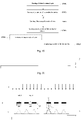
- FIG. 9 shows a flowchart of a method for manufacturing a display substrate according to an embodiment of the present disclosure.
- the method for manufacturing the display substrate may include steps S901 to S903. Referring to FIGS. 1a and 9 , in step S901, a substrate 1 is provided. In step S902, the first electrode 2 is formed on the substrate 1. In step S903, a conductive convex 3 is formed on the first electrode 2.
- the dimension of the cross section S1 of the conductive convex 3 along a plane parallel to the substrate 1 is negatively correlated to the distance D1 from the cross section S1 to the surface of the first electrode 2.
- the negative correlation means that as the distance D1 is larger, the dimension of the cross section S1 is smaller.
- the dimension of the cross section S1 here may refer to, for example, the area of the cross section S1, and the surface of the first electrode 2 refers to the surface of the first electrode 2 that is in contact with the conductive convex 3.
- the number of conductive convexes may be one or more, which is not specifically limited in the present disclosure.
- the method for forming the conductive convex 3 is specifically described below.
- FIG. 10 shows a flowchart of a method for forming conductive convexes according to an embodiment of the present disclosure.
- a dielectric material layer 3' is formed on the substrate 1 and the first electrode 2.
- step S9032 the dielectric material layer is patterned to form a first portion of the conductive convex.
- the material of the dielectric material layer may include a photosensitive material. Further, as an example, the material of the dielectric material layer includes an organic photosensitive material.
- patterning the dielectric material layer 3' may include exposing the dielectric material layer 3' using a first mask M1 and developing the dielectric material layer 3' to form a first portion 31 of the conductive convex 3 (as shown by the dotted line portion in FIG. 12 ).
- a radiation dose of a light L for exposing the dielectric material layer 3', a dimension D6 of a light shielding portion M1-1 of the first mask M1 along a direction perpendicular to the direction in which the light shielding portion M1-1 extends, and a distance D7 from the first mask M1 to the dielectric material layer 3' are configured such that a diffracted light L D is generated at an edge of the light shielding portion M1-1 during exposure.
- At least a portion of the diffracted light L D can reach the surface of the dielectric material layer 3' located below the central portion C of the light shielding portion M1-1. Since the intensity of the diffracted light L D incident on the corresponding portion of the dielectric material directly located below the central portion C decreases as the distance from the light shielding portion M1-1 to the corresponding portion decreases, thereby forming an unexposed portion having a convex shape of the corresponding portion of the dielectric material as indicated by the dotted line in FIG. 12 . The unexposed portion will form the first portion 31 of the conductive convex 3.
- a ratio of the dimension D6 of the light shielding portion M1-1 of the first mask M1 to a dimension D8 of the non-light shielding portion M1-1 of the first mask M1 can range from 1: 1 to 3: 2.
- the distance between the mask and the structure to be exposed is generally fixed.
- the radiation dose of the light L may be increased.
- the distance D7 from the first mask M1 to the dielectric material layer 3' is smaller (even in contact state)
- the radiation dose of the light L can be reduced.
- patterning the dielectric material layer 3' may include imprinting the dielectric material layer 3', thereby obtaining the first portion 31 of the conductive convex 3.
- a surface of the imprint head for imprinting may have a concave structure corresponding to the convex.
- step S9033 a second portion of the conductive convex is formed.
- a first conductive material layer 3" is formed on the surface of the substrate 1, the first electrode 2, and the first portion 31 of the conductive convex.
- the method for forming the first conductive material layer 3" may include, for example, a sputtering method.
- step S9034 a second portion of the conductive convex is formed.
- the first conductive material layer 3" is patterned to form the second portion 32 of the conductive convex 3.
- the resulting structure is shown in FIG. 15 .
- the patterning may use a photolithography method commonly used in the art, which is not specifically limited herein.
- the conductive convex 3 may include a first portion 31 and a second portion 32 covering the first portion 31.
- An orthographic projection of the first portion 31 on the substrate 1 may be located within an orthographic projection of the first electrode 2 on the substrate 1.
- the second portion 32 may contact the first electrode 2.
- a surface 311 of the first portion 31 away from the substrate 1 may be conformal to a surface 321 of the second portion 32 away from the substrate 1.
- the second portion 32 of the conductive convex 3 may also be located on the surface of the first electrode 2 which is not covered by the first portion 31, thereby forming a more effective electrical connection between the conductive convex 3 and the first electrode 2.
- step S9035 may be included between step S9032 and step S9033. That is, before forming the first conductive material layer 3", referring to FIG. 13 , the surface of the first portion 31 of the conductive convex 3 may be roughened. As an example, the roughening may include a micro etching process. Thereby, during the formation of the first conductive material layer 3", the adhesion of the first conductive material layer 3" on the first portion 31 of the conductive convex 3 can be increased.
- the formation of the first conductive material layer 3" by the sputtering method may cause the top of the first portion 31 of the conductive convex to collapse.
- at least one of the following two methods can be used.
- the first method is to reduce the deposition power of the first conductive material layer. That is, multiple times deposition method are used, but a small amount of conductive material is deposited each time, thereby improving the problem of collapse.
- the second method is to form an inorganic material layer on the conductive convex after forming the first portion of the conductive convex and before forming the first conductive material layer.
- a step S9036 for forming an inorganic material layer may be included between step S9032 and step S9033.
- an inorganic material layer 33 may be formed on the surface of the first portion 31 after forming the first portion 31 and before forming the first conductive material layer 3".
- the inorganic material layer 33 may be formed on the surface of the first portion 31 after roughening the surface of the first portion 31 and before forming the first conductive material layer 3".
- a surface of the inorganic material layer 33 is conformal to the surface of the first portion 31 away from the substrate 1.
- the material of the inorganic material layer 33 may include, for example, silicon nitride (SiN x ), silicon oxide (SiO x ), or the like.
- a process conventionally used in the art such as CVD can be used as long as the first portion 31 does not undergo undesirable deformation such as collapse.
- FIG. 18 shows a flowchart of a method for forming a conductive convex according to an embodiment of the present disclosure. As shown in FIG. 18 , the method for forming the conductive convex includes steps S9031' and S9032'.
- a second conductive material layer 3′′′ is formed on the substrate 1.
- the method for forming the second conductive material layer 3′′′ may include, for example, a sputtering method.
- step S9032' the second conductive material layer 3′′′ is patterned to form the first electrode 2 and the conductive convex 3 located on the first electrode 2.
- the patterning may include a conventional photolithography method, which is not specifically limited herein.
- the ratio of the thickness T1 of the first electrode 2 to the distance D3 from the top of the conductive convex 3 to the bottom of the first electrode 2 may range from 1: 4 to 1: 2.
- the thickness T1 may be 0.5 ⁇ m.
- the range of the distance D3 may be 1-2 ⁇ m.
- the conductive material may include aluminum, copper, molybdenum, titanium, tungsten, or the like.
- the method for manufacturing a display substrate may further include steps S904 to S906, as shown by the steps within the dotted frame in the flowchart in FIG. 20 .
- an adhesive layer is applied. Specifically, an adhesive layer 5 is applied on and between the conductive convexes 3 so that the adhesive layer covers the top of the conductive convexes. In an exemplary embodiment of the present disclosure, a top surface of the adhesive layer 5 is higher than the top of the conductive convex 3 by about 1 ⁇ m.
- step S905 referring to FIG. 21 , an electronic device and the adhesive layer are joined to obtain the structure shown in FIG. 7a .
- the electronic device 4 is placed over the adhesive layer 5 and a force F is applied to the electronic device 4 to cause the conductive convex 3 to penetrate the adhesive layer 5 and contact the electronic device 4, thereby the electronic device 4 is joined together with the first electrode 2 by the adhesive layer 5.
- a mass transfer technique is used to simultaneously transfer a plurality of electronic devices 4 to the adhesive layer 5 (for example, resin material).
- the pins 41 and 42 of the electronic device 4 are in contact with the conductive convexes 3. At this time, the pins 41, 42 of the electronic device 4 enter into the resin material.
- the mass transfer technique refers to simultaneously transfer a large number of electronic devices to the structure described above with reference to FIGS. 1a and 2-5 (hereinafter, referred as an intermediate structure) by means of vacuum, static electricity, stickiness, etc.
- the side of the intermediate structure having the conductive convexes 3 is facing upward to facilitate the joining with the electronic device 4.
- the adhesive layer 5 for example, a resin material
- the resin material may overflow around.
- a certain pressure is needed for the electronic device 4 entering into the resin material, so that the pins 41 and 42 of the electronic device 4 are in contact with the top of the conductive convex.
- the entry of the electronic device 4 causes the resin material to overflow around.
- the contact state between the conductive convexes 3 and the pins 41, 42 shown in FIG. 7a is only exemplary, and which is not specifically limited herein. In practical applications, the top of the conductive convex 3 may be allowed to deform to fit the shape of the pins 41, 42 as shown in FIG. 7b .
- the top of the conductive convex 3 can be penetrate into the pins 41, 42 to achieve more effective electrical and mechanical connection, as shown in FIG. 7c .
- the adhesive layer 5 is cured.
- the material of the adhesive layer 5 may include resin.
- the resin may contain a solvent, for example.
- curing may be performed using a commonly used thermal curing process.
- the resin material is heated to cure the resin material.
- the temperature of heating may be about 140 °C.
- the surface tension of the resin material will drive the electronic device 4 to be pressed down.
- the top of the conductive convex 3 pierces the resin material wrapped around the top thereof, thereby achieving electrical connection between the electronic device 4 and the first electrode 2.
- the material hardness of the pins 41 and 42 of the electronic device 4 is less than that of the conductive convex 3
- the top of the conductive convex 3 is finally penetrated into the pins 41 and 42 under the aforementioned tension, thereby the electrical connection between the electronic device 4 and the first electrode 2 is further guaranteed.
- the firmness of the electrical connection is also ensured.
- the method for manufacturing the display substrate may further include steps S2301 to S2307, as shown in the flowchart in FIG. 22 .
- step S2301 a thin film transistor is formed. Specifically, the thin film transistor 6 is formed on the first substrate 1.
- forming the thin film transistor 6 may include: forming a buffer layer 61 on the substrate 1; forming an active layer material layer on the buffer layer 61; patterning the active layer material layer to form the active layer 62; forming an insulating layer 63 on the buffer layer 61 and the active layer 62; forming a gate material layer on the insulating layer 63; and patterning the gate material layer to form the gate layer 64.
- a first sub-dielectric layer is formed. Specifically, the first sub-dielectric layer 71 is formed on the insulating layer 63 and the gate layer 64. As an example, the first sub-dielectric layer 71 may be an interlayer insulating layer.
- a first hole is formed in the first sub-dielectric layer. Specifically, a first hole 711 exposing the source/drain region of the thin film transistor 6 (i.e., exposing the active layer 62) is formed in the first sub-dielectric layer 71 through processes such as exposure, development, and etching.
- a third conductive material layer is formed. Specifically, a third conductive material layer is formed on the first sub-dielectric layer 71.
- step S2305 the second electrode and the third electrode are formed. Specifically, the third conductive material layer is patterned to form the second electrode 81 and the third electrode 82.
- the second electrode 81 may be the source/drain electrode of the thin film transistor 7.
- the second electrode 81 may be connected to the active layer 62 of the thin film transistor 6 via the first hole 711.
- the third electrode 82 may be a wiring in the display substrate 100.
- a second sub-dielectric layer is formed.
- the second sub-dielectric layer 72 is formed on the first sub-dielectric layer 71, the second electrode 81 and the third electrode 82.
- the second sub-dielectric layer 72 may be a passivation layer or a planarization layer.
- a second hole and a third hole are formed in the second sub-dielectric layer.
- the second sub-dielectric layer 72 is patterned to form the second and the third holes 721 and 722 in the second sub-dielectric layer 72.
- the second hole 721 exposes the second electrode 81 and the third hole exposes the third electrode 82.
- the first electrode 2 may include a first sub-electrode 21 and a second sub-electrode 22.
- the first sub-electrode 21 is connected to the second electrode 81 via the second hole 721 in the second sub-dielectric layer 72.
- the second sub-electrode 22 is connected to the third electrode 82 via the third hole 722 in the second sub-dielectric layer 72.
- the first electrode 2 may be a bonding pad used to bond the electronic device 4.
- the electronic device 4 can be controlled by the thin film transistor 7.
- the thin film transistor 7 may control the light emission of the micro LED via the first electrode 2 and the conductive convex 3.
Landscapes
- Devices For Indicating Variable Information By Combining Individual Elements (AREA)
- Electroluminescent Light Sources (AREA)
- Led Device Packages (AREA)
- Electrochromic Elements, Electrophoresis, Or Variable Reflection Or Absorption Elements (AREA)
Abstract
Description
- Embodiments of the present disclosure relate to a field of displaying technology, in particular, to a display substrate and a method for manufacturing the same.
- Micro LED is regarded as the next-generation display technology which is most likely to replace OLED.
- The advantages of micro LED include low power consumption, high brightness, ultra-high resolution and color saturation, fast response, ultra power saving, long lifetime, high efficiency, adaptability to various dimensions, seamless stitching, etc. The power consumption of micro LED is 10% of LCD and 50% of OLED, so it is suitable for wearable devices.
- Embodiments of the present disclosure provide a display substrate and a method for manufacturing the same.
- In one aspect of the present disclosure, a display substrate is provided. The display substrate includes: a substrate; a first electrode located on the substrate; and a conductive convex located on the first electrode. A dimension of a cross section of the conductive convex along a plane parallel to the substrate is negatively correlated to a distance from the cross section to a surface of the first electrode.
- In an exemplary embodiment of the present disclosure, a ratio of a minimum dimension of a surface of a side of the conductive convex facing the substrate along a direction parallel to the substrate to a distance from the conductive convex to the first electrode ranges from 1: 1 to 1: 3.
- In an exemplary embodiment of the present disclosure, a shape of the conductive convex is at least one selected from a group consisting of a cone, a truncated cone, and a prism.
- In an exemplary embodiment of the present disclosure, the conductive convex includes a first portion and a second portion covering the first portion. An orthographic projection of the first portion on the substrate is located within an orthographic projection of the first electrode on the substrate. The second portion is in contact with the first electrode. A surface of the second portion away from the substrate is conformal to a surface of the first portion away from the substrate. The first portion is composed of a dielectric material, and the second portion is composed of a conductive material.
- In an exemplary embodiment of the present disclosure, the dielectric material includes an organic material. The conductive convex further includes an inorganic material layer covering the first portion and located between the first portion and the second portion.
- In an exemplary embodiment of the present disclosure, the second portion further covers a surface of the first electrode adjacent to the first portion.
- In an exemplary embodiment of the present disclosure, the conductive convex is composed of a conductive material.
- In an exemplary embodiment of the present disclosure, the first electrode is formed integrally with the conductive convex. A ratio of a thickness of the first electrode to a distance from a top of the conductive convex to a bottom of the first electrode ranges from 1: 4 to 1: 2.
- In an exemplary embodiment of the present disclosure, a plurality of conductive convexes arranged in an array are disposed on each of the first electrodes.
- In an exemplary embodiment of the present disclosure, the conductive convex includes a triangular prism. The triangular prism includes a first surface parallel to the surface of the substrate, the first surface includes a first side and a second side intersecting the first side. A dimension of the first side is 2-10µm. A dimension of the second side is 1-5µm. A height of the triangular prism along a direction perpendicular to the substrate is 1-5µm. A distance between two adjacent conductive convexes in a direction of the first side is 2-10µm. A distance between two adjacent conductive convexes in a direction of the second side is 2-5µm.
- In an exemplary embodiment of the present disclosure, the display substrate further includes: an electronic device located on the conductive convex; and an adhesive located between the conductive convexes. A pin of the electronic device is in contact with the conductive convex. The pin is joined to the first electrode by the adhesive.
- In an exemplary embodiment of the present disclosure, the display substrate further includes: a thin film transistor located on the substrate; and a first dielectric layer located on the thin film transistor. The first electrode is located on the first dielectric layer and is electrically connected to the thin film transistor.
- In an exemplary embodiment of the present disclosure, the first dielectric layer includes a first sub-dielectric layer and a second sub-dielectric layer sequentially stacked. The display substrate further includes a second electrode and a third electrode located between the first sub-dielectric layer and the second sub-dielectric layer. The second electrode is connected to a source/drain region of the thin film transistor via a first hole in the first sub-dielectric layer. The first electrode includes a first sub-electrode and a second sub-electrode. The first sub-electrode is connected to the second electrode via a second hole in the second sub-dielectric layer. The second sub-electrode is connected to the third electrode via a third hole in the second sub-dielectric layer.
- In one aspect of the present disclosure, a method for manufacturing a display substrate is provided. The method includes: provide a substrate; forming a first electrode on the substrate; and forming a conductive convex on the first electrode. A dimension of a cross section of the conductive convex along a plane parallel to the substrate is negatively correlated to a distance from the cross section to a surface of the first electrode.
- In an exemplary embodiment of the present disclosure, forming the conductive convex includes: forming a dielectric material layer on the first electrode; patterning the dielectric material layer to form a first portion of the conductive convex; forming a first conductive material layer on the substrate, the first electrode, and the first portion; and patterning the first conductive material layer to form a second portion of the conductive convex. An orthographic projection of the first portion on the first electrode is located within an orthographic projection of the second portion on the first electrode. The second portion covers the first electrode and is in contact with the first electrode. A surface of the second portion away from the substrate is conformal to a surface of the first portion away from the substrate.
- In an exemplary embodiment of the present disclosure, before forming the first conductive material layer on the first portion, the method further includes roughening a surface of the first portion.
- In an exemplary embodiment of the present disclosure, the second portion is formed to also cover a surface of the first electrode adjacent to the first portion.
- In an exemplary embodiment of the present disclosure, the dielectric material layer includes a photosensitive material. Patterning the dielectric material layer includes exposing the dielectric material layer using a first mask and developing the dielectric material layer. A radiation dose of a light used for the exposure, a dimension of a light shielding portion of the first mask along a direction perpendicular to a direction in which the light shielding portion extends, and a distance between the first mask and the dielectric material layer are configured such that a diffracted light is generated at an edge of the light shielding portion during the exposure, wherein at least a portion of the diffracted light can reach a surface of the dielectric material layer located below a central portion of the light shielding portion.
- In an exemplary embodiment of the present disclosure, forming the conductive convex further includes: forming an inorganic material layer on the first portion after forming the first portion and before forming the first conductive material layer. A surface of the inorganic material layer away from the substrate is conformal to a surface of the first portion away from the substrate.
- In an exemplary embodiment of the present disclosure, forming the first electrode on the substrate and forming the conductive convex on the first electrode include: forming a second conductive material layer on the substrate; and patterning the second conductive material layer to form the first electrode and the conductive convex located on the first electrode.
- In an exemplary embodiment of the present disclosure, the method further includes: forming an adhesive layer to cover the conductive convex and a portion of the first electrode located between the conductive convexes; placing an electronic device on the adhesive layer and applying a force to the electronic device so that the conductive convex penetrates the adhesive layer and contacts the electronic device; and curing the adhesive layer.
- Adaptive and further aspects and scope will become apparent from the description provided herein. It should be understood that various aspects of this disclosure may be implemented individually or in combination with one or more other aspects. It should also be understood that the description and specific examples herein are intended for purposes of illustration only and are not intended to limit the scope of the present disclosure.
- The drawings described herein are for illustrative purposes only of selected embodiments and not all possible implementations, and are not intended to limit the scope of the present application.
-
FIG. 1a shows a schematic view of a cross section of a display substrate according to an embodiment of the present disclosure. -
FIGS. 1b to 1f show schematic views of shapes of conductive convexes according to an embodiment of the present disclosure. -
FIG. 2 shows a schematic view of a cross section of a display substrate according to another embodiment of the present disclosure. -
FIG. 3 shows a schematic view of a cross section of a display substrate according to yet another embodiment of the present disclosure. -
FIG. 4 shows a schematic view of a cross section of a display substrate according to yet another embodiment of the present disclosure. -
FIG. 5 shows a schematic view of a cross section of a display substrate according to yet another embodiment of the present disclosure. -
FIG. 6 shows a perspective view of a display substrate according to an embodiment of the present disclosure. -
FIGS. 7a to 7c show schematic views of cross sections of a display substrate according to yet another embodiment of the present disclosure. -
FIG. 8 shows a schematic view of a cross section of a display substrate according to yet another embodiment of the present disclosure. -
FIG. 9 shows a flowchart of a method for manufacturing a display substrate according to an embodiment of the present disclosure. -
FIGS. 10 to 17 show schematic views of a method for forming a conductive convex according to an embodiment of the present disclosure. -
FIGS. 18 to 22 show schematic views of a method for forming a conductive convex according to another embodiment of the present disclosure. - Corresponding reference numerals indicate corresponding parts or features throughout the several views of the drawings.
- As used herein and in the appended claims, the singular form of a word includes the plural, and vice versa, unless the context clearly dictates otherwise. Thus, the references "a", "an", and "the" are generally inclusive of the plurals of the respective terms. Similarly, the words "comprise", "comprises", and "comprising" are to be interpreted inclusively rather than exclusively. Likewise, the terms "include", "including" and "or" should all be construed to be inclusive, unless such a construction is clearly prohibited from the context. The term "example" used herein, particularly when followed by a listing of terms, is merely exemplary and illustrative and should not be deemed to be exclusive or comprehensive.
- Additionally, further to be noted, when the elements and the embodiments thereof of the present application are introduced, the articles "a/an", "one", "the" and "said" are intended to represent the existence of one or more elements. Unless otherwise specified, "a plurality of' means two or more. The expressions "comprise", "include", "contain" and "have" are intended as inclusive and mean that there may be other elements besides those listed. The terms such as "first" and "second" are used herein only for purposes of description and are not intended to indicate or imply relative importance and the order of formation.
- In addition, in the drawings, the thickness and area of each layer are exaggerated for clarity. It should be understood that when a layer, a region, or a component is referred to as being "on" another part, it is meant that it is directly on the another part, or there may be other components in between. In contrast, when a certain component is referred to as being "directly" on another component, it is meant that no other component lies in between.
- The flow diagrams depicted herein are just one example. There may be many variations to this diagram or the steps (or operations) described therein without departing from the spirit of the disclosure. For instance, the steps may be performed in a differing order or steps may be added, deleted or modified. All of these variations are considered a part of the claimed disclosure.
- Exemplary embodiments will now be described more fully with reference to the accompanying drawings.
- At present, micro LED technology confronts quite a few technical challenges. The transfer and bonding of micro LED is one of the key technologies in micro LED technology.
- In the related art, there are four methods for bonding micro LEDs. The first method is to use solder paste for bonding, but the solder paste needs to be heated during bonding, and heating will unnecessarily degrade the performance of the micro LED. The second method is to use anisotropic conductive adhesive for bonding, but the cost of anisotropic conductive adhesive is higher. The third method is to use die bonding welding for bonding, but applying pressure to the display substrate during bonding will adversely affect the characteristics of electronic elements such as thin film transistors in the display substrate. The fourth method is to use the way of metal directly contacting metal to transfer micro LED, but the adhesive between metal and metal is not easy to be discharged, which will reduce the contacting area between metal and metal.
- Embodiments of the present disclosure provide a display substrate including conductive convexes. The conductive convex is configured to be easily connected to the micro LED, thereby reducing the manufacturing cost and improving the transferring efficiency for the micro LED.
-
FIG. 1a shows a schematic view of a cross section of a display substrate according to an embodiment of the present disclosure. As shown inFIG. 1a , thedisplay substrate 100 includes: asubstrate 1; afirst electrode 2 located on thesubstrate 1; and a conductive convex 3 located on thefirst electrode 2. - In an exemplary embodiment of the present disclosure, referring to
FIG. 1a , a dimension of a cross section S1 of the conductive convex 3 along a plane parallel to thesubstrate 1 is negatively correlated to a distance D1 from the cross section S1 to a surface of thefirst electrode 2. Here, the negative correlation means that as the distance D1 is larger, the dimension of the cross section S1 is smaller. It should be noted that the dimension of the cross section S1 here may refer to, for example, the area of the cross section S1, and the surface of thefirst electrode 2 refers to the surface of thefirst electrode 2 that is in contact with the conductive convex 3. In addition, in an exemplary embodiment of the present disclosure, the number of conductive convexes may be one or more, which is not specifically limited in the present disclosure. - It should be noted that in
FIG. 1a and other drawings to be described below, the proportional relationship between the dimensions of the components cannot be regarded as a limit to the present disclosure. It can be understood that, in order to clearly depict the structure of a certain component, the dimension of this component may be depicted as being larger than the dimension of other parts. The drawings of the present disclosure are merely exemplary and should not be considered as a limit to the present disclosure. - In an exemplary embodiment of the present disclosure, the ratio of the area of an orthographic projection of the
conductive convexes 3 on the surface of thefirst electrode 2 to the surface area of thefirst electrode 2 may be greater than 20%, for example. - In an exemplary embodiment of the present disclosure, with continued reference to
FIG. 1a , the ratio of the minimum dimension L1 of a surface of a side of the conductive convex 3 facing thesubstrate 1 along a direction parallel to thesubstrate 1 to a distance D2 from a top of the conductive convex 3 to theelectrode 2 can range from 1: 1 to 1: 3. - In an exemplary embodiment of the present disclosure, a shape of the conductive convex 3 may be at least one selected from a group consisting of: a cone, a truncated cone, and a prism. As an example, in
FIG. 1a , for example, the shape of the conductive convex may include a prism. -
FIGS. 1b to 1f show schematic views of shapes of conductive convexes according to an embodiment of the present disclosure. The shapes of the conductive convex 3 inFIGS. 1b to 1f may be irregular shapes. For example, inFIG. 1b , the shape of the conductive convex 3 may be a cone with an arc-shaped side. For example, inFIGS. 1c to 1f , the conductive convex 3 may have a plurality of tips. - The structure of the conductive convex 3 of the embodiment of the present disclosure is specifically described below.
- On the one hand, in an embodiment of the present disclosure, the conductive convex 3 includes a first portion and a second portion covering the first portion.
- Specifically,
FIG. 2 shows a schematic view of a cross section of a display substrate according to an embodiment of the present disclosure. In an exemplary embodiment of the present disclosure, as shown inFIG. 2 , the conductive convex 3 may include afirst portion 31 and asecond portion 32 covering thefirst portion 31. For example, an orthographic projection of thefirst portion 31 on thesubstrate 1 may be located within an orthographic projection of thefirst electrode 2 on thesubstrate 1. Thesecond portion 32 may contact thefirst electrode 2. Asurface 311 of thefirst portion 31 away from thesubstrate 1 may be conformal to asurface 321 of thesecond portion 32 away from thesubstrate 1. That is, the shape of a side of thefirst portion 31 away from thesubstrate 1 and the shape of a side of thesecond portion 32 away from thesubstrate 1 are similar shapes. - In an exemplary embodiment of the present disclosure, the
first portion 31 of the conductive convex 3 may be composed of a dielectric material. In an exemplary embodiment of the present disclosure, thesecond portion 32 of the conductive convex 3 may be composed of a conductive material. - As an example, the dielectric material may include an organic material. Further, as an example, the organic material may include an organic resin material. For example, the organic resin material may include polyimide-type resin or acrylic-type resin.
- As an example, the conductive material may include aluminum, copper, molybdenum, titanium, tungsten, or the like.
- In an exemplary embodiment of the present disclosure, the material of the
second portion 32 of the conductive convex 3 may be the same as or different from the material of thefirst electrode 2. Those skilled in the art can select according to needs or manufacturing processes, etc., and the present disclosure does not specifically limit this. -
FIG. 3 shows a schematic view of a cross section of a display substrate according to an embodiment of the present disclosure. Further, as an alternative embodiment of the present disclosure, as shown inFIG. 3 , the conductive convex 3 may further include an inorganic material layer 33 covering thefirst portion 31 and located between thefirst portion 31 and thesecond portion 32. It should be noted that the inorganic material layer 33 may protect the underlying dielectric material (i.e., the first portion 31) during manufacturing thesecond portion 32 of the conductive convex 3. For example, when thesecond portion 32 is formed by sputtering, the sputtered ions (e.g., metal ions) continue to impact the surface of thefirst portion 31 and generate a large amount of heat, which causes the dielectric material such as an organic material of the second portion to have deformation such as collapse. - In an exemplary embodiment of the present disclosure, the material of the inorganic material layer 33 may include, for example, silicon nitride (SiNx), silicon oxide (SiOx), or the like.
-
FIG. 4 shows a schematic view of a cross section of a display substrate according to an embodiment of the present disclosure. Further, as an alternative embodiment of the present disclosure, thesecond portion 32 of the conductive convex 3 may also cover the surface of thefirst electrode 2 that is exposed and located between two adjacentfirst portions 31, as shown by the dotted circle inFIG. 4 . This arrangement enables a more effective electrical connection between the conductive convex 3 and thefirst electrode 2, and thereby further reducing the contact resistance. - On the other hand, in an embodiment of the present disclosure, the conductive convex 3 may be composed of only a conductive material.
- In an embodiment of the present disclosure, the
first electrode 2 and the conductive convex 3 may be integrally formed. That is, thefirst electrode 2 and the conductive convex 3 are made of the same material and formed by the same step. -
FIG. 5 shows a schematic view of a cross section of a display substrate according to an embodiment of the present disclosure. As shown inFIG. 5 , a ratio of the thickness T1 of thefirst electrode 2 to the distance D3 from the top of the conductive convex 3 to the bottom of thefirst electrode 2 may range from 1: 4 to 1: 2. As an example, the thickness T1 may be 0.5µm. As an example, the range of the distance D3 may be 1-2µm. - Similar to the above embodiment, in this embodiment, for example, the conductive material may include aluminum, copper, molybdenum, titanium, tungsten, or the like.
-
FIG. 6 shows a perspective view of thedisplay substrate 100 according to an embodiment of the present disclosure. In an exemplary embodiment of the present disclosure, as shown inFIG. 6 , a plurality ofconductive convexes 3 arranged in an array are provided on eachfirst electrode 2. It should be noted that the number ofconductive convexes 3 shown inFIG. 6 is only exemplary and should not be considered as a limit to the present disclosure. - As shown in
FIG. 6 , as an alternative embodiment, the conductive convex 3 may include a triangular prism. In this embodiment, thetriangular prism 3 may include a first surface S2 parallel to the surface of thesubstrate 1. The first surface S2 may include a first side L2 and a second side L3 intersecting the first side L2. As an example, the distance D4 between two adjacent conductive convexes 3 (i.e., the triangular prism 3) along the extending direction of the first side L2 (i.e., the X direction) may range from 2 to 10µm. As an example, the distance D5 between two adjacent conductive convexes 3 (i.e., triangular prisms 3) along the extending direction of the second side L3 (i.e., Y direction) may range from 2 to 5µm. As an example, the dimension of the first side L2 may range from 2-10µm, the dimension of the second side L3 may range from 1-5µm, and the range of the height H1 of thetriangular prism 3 along the direction perpendicular to thesubstrate 1 may be 1-5µm. - As an alternative embodiment, the
triangular prism 3 may include a regular triangular prism, as shown inFIG. 6 . -
FIG. 7a shows a schematic view of a cross section of a display substrate according to an embodiment of the present disclosure. Further, as shown inFIG. 7a , thedisplay substrate 100 may further include: anelectronic device 4 located on the conductive convex 3; and an adhesive 5 located between theconductive convexes 3. - In an exemplary embodiment of the present disclosure, the
pins electronic device 4 may be in contact with the conductive convex 3. The adhesive 5 joins thepins first electrode 2. It should be noted that the distances D4, D5 between theconductive convexes 3 inFIG. 6 are configured to more effectively discharge the adhesive 5 from the joined position when thepins first electrode 2 are joined by the adhesive 5, thereby achieving good electrical contact between thepins first electrode 2. - It should be noted that the contact state between the conductive convex 3 and the
pins FIG. 7a is only exemplary (the structures ofFIGS. 8 and22 are also exemplary hereinafter), which is not specifically limited herein. In practical applications, the top of the conductive convex 3 may be allowed to deform to fit the shape of thepins FIG. 7b . - In addition, when the hardness of the material of the conductive convex 3 is greater than the hardness of the material of the
pins pins Figure 7c . - In an exemplary embodiment of the present disclosure, the
electronic device 4 may include a micro LED. - As an example, the material of the adhesive 5 may include silicone-based glue, resin-based glue, photocurable glue, or the like. As an example, the photocurable glue may include an acrylate-based prepolymer (also referred as oligomer), a reactive monomer, an ultraviolet photoinitiator, or the like.
FIG. 8 shows a schematic view of a cross section of a display substrate according to an embodiment of the present disclosure. Further, as shown inFIG. 8 , thedisplay substrate 100 may further include: a thin film transistor 6 located on thesubstrate 1; and a first dielectric layer 7 located on the thin film transistor 6. In this embodiment, thefirst electrode 2 is located on the first dielectric layer 7 and is electrically connected to the thin film transistor 6. In an exemplary embodiment of the present disclosure, as shown inFIG. 8 , the thin film transistor 7 may include: abuffer layer 61 located on thesubstrate 1; anactive layer 62 located on thebuffer layer 61; an insulatinglayer 63 covering thebuffer layer 61 and theactive layer 62; and agate layer 64 located on the insulatinglayer 63. Although the thin film transistor 7 shown inFIG. 8 is a top-gate thin film transistor, the thin film transistor 7 may also be a bottom-gate thin film transistor. A person skilled in the art can select the type of thin film transistor according to needs. The thin film transistor 7 shown inFIG. 8 is merely exemplary and should not be considered as a limit to the present disclosure. - In an embodiment of the present disclosure, as shown in
FIG. 8 , the first dielectric layer 7 may include a firstsub-dielectric layer 71 and a secondsub-dielectric layer 72 sequentially stacked. The firstsub-dielectric layer 71 may cover the insulatinglayer 63 and thegate layer 64. As an example, the firstsub-dielectric layer 71 may be an interlayer insulating layer. As an example, the secondsub-dielectric layer 72 may be a passivation layer or a planarization layer. - In addition, with continued reference to
FIG. 8 , thedisplay substrate 100 may further include asecond electrode 81 and athird electrode 82 located between the firstsub-dielectric layer 71 and the secondsub-dielectric layer 72. In an exemplary embodiment of the present disclosure, thesecond electrode 81 may be connected to the source/drain region of the thin film transistor 6 via a first hole 711 in the firstsub-dielectric layer 71. - In an exemplary embodiment of the present disclosure, the
second electrode 81 may be disposed in the same layer as thethird electrode 82. That is, thesecond electrode 81 and thethird electrode 82 may be composed of the same material and formed by the same step. As an example, thesecond electrode 81 may be the source/drain electrode of the thin film transistor 7. As an example, thethird electrode 82 may be a wiring in thedisplay substrate 100. - Further, In an exemplary embodiment of the present disclosure, with continued reference to
FIG. 8 , thefirst electrode 2 may include afirst sub-electrode 21 and asecond sub-electrode 22. The first sub-electrode 21 may be connected to thesecond electrode 81 via asecond hole 721 in the secondsub-dielectric layer 72. The second sub-electrode 22 may be connected to thethird electrode 82 via athird hole 722 in the secondsub-dielectric layer 72. As an example, thefirst electrode 2 may be a bonding pad used to bond theelectronic device 4. - In an embodiment of the present disclosure, for example, after the
electronic device 4 is bonded to thefirst electrode 2, theelectronic device 4 can be controlled by the thin film transistor 7. As an example, when theelectronic device 4 includes a micro LED, the thin film transistor 7 may control the light emission of the micro LED by thefirst electrode 2 and the conductive convex 3. - In an embodiment of the present disclosure, a method for manufacturing a display substrate is also provided. The display substrate manufactured according to the embodiments of the present disclosure includes conductive convexes. The conductive convex is configured to be easily connected to the micro LED, thereby being able to reduce the manufacturing cost and improve the bonding yield of the micro LED.
-
FIG. 9 shows a flowchart of a method for manufacturing a display substrate according to an embodiment of the present disclosure. As shown inFIG. 9 , the method for manufacturing the display substrate may include steps S901 to S903. Referring toFIGS. 1a and9 , in step S901, asubstrate 1 is provided. In step S902, thefirst electrode 2 is formed on thesubstrate 1. In step S903, a conductive convex 3 is formed on thefirst electrode 2. - Similar to the description about
FIG. 1a , in an exemplary embodiment of the present disclosure, referring toFIG. 1a , the dimension of the cross section S1 of the conductive convex 3 along a plane parallel to thesubstrate 1 is negatively correlated to the distance D1 from the cross section S1 to the surface of thefirst electrode 2. Here, the negative correlation means that as the distance D1 is larger, the dimension of the cross section S1 is smaller. It should be noted that the dimension of the cross section S1 here may refer to, for example, the area of the cross section S1, and the surface of thefirst electrode 2 refers to the surface of thefirst electrode 2 that is in contact with the conductive convex 3. In addition, in an exemplary embodiment of the present disclosure, the number of conductive convexes may be one or more, which is not specifically limited in the present disclosure. - For some description about the conductive convex 3, reference may be made to the description about
FIGS. 1a to 1f , which will not be repeated here. - The method for forming the conductive convex 3 is specifically described below.
- On the one hand, the process for forming the conductive convex 3 according to an embodiment of the present disclosure is described with reference to
FIGS. 10 to 17 , and the structure of the formed conductive convex 3 is shown inFIG. 2 . -
FIG. 10 shows a flowchart of a method for forming conductive convexes according to an embodiment of the present disclosure. Referring toFIGS. 10 and 11 , in step S9031, a dielectric material layer 3' is formed on thesubstrate 1 and thefirst electrode 2. - With continued reference to
FIG. 10 , in step S9032, the dielectric material layer is patterned to form a first portion of the conductive convex. - In an exemplary embodiment of the present disclosure, the material of the dielectric material layer may include a photosensitive material. Further, as an example, the material of the dielectric material layer includes an organic photosensitive material.
- For a material example of the dielectric material layer, reference may be made to the description about
FIG. 2 above, and details are not repeated here. - Specifically, in the case where the material of the dielectric material layer may include a photosensitive material, as shown in
FIG. 12 , patterning the dielectric material layer 3' may include exposing the dielectric material layer 3' using a first mask M1 and developing the dielectric material layer 3' to form afirst portion 31 of the conductive convex 3 (as shown by the dotted line portion inFIG. 12 ). - In an exemplary embodiment of the present disclosure, a radiation dose of a light L for exposing the dielectric material layer 3', a dimension D6 of a light shielding portion M1-1 of the first mask M1 along a direction perpendicular to the direction in which the light shielding portion M1-1 extends, and a distance D7 from the first mask M1 to the dielectric material layer 3' are configured such that a diffracted light LD is generated at an edge of the light shielding portion M1-1 during exposure.
- In an exemplary embodiment of the present disclosure, at least a portion of the diffracted light LD can reach the surface of the dielectric material layer 3' located below the central portion C of the light shielding portion M1-1. Since the intensity of the diffracted light LD incident on the corresponding portion of the dielectric material directly located below the central portion C decreases as the distance from the light shielding portion M1-1 to the corresponding portion decreases, thereby forming an unexposed portion having a convex shape of the corresponding portion of the dielectric material as indicated by the dotted line in
FIG. 12 . The unexposed portion will form thefirst portion 31 of the conductive convex 3. - In an exemplary embodiment of the present disclosure, with continued reference to
FIG. 12 , a ratio of the dimension D6 of the light shielding portion M1-1 of the first mask M1 to a dimension D8 of the non-light shielding portion M1-1 of the first mask M1 can range from 1: 1 to 3: 2. - In addition, in the conventional exposure process, the distance between the mask and the structure to be exposed is generally fixed. In an exemplary embodiment of the present disclosure, when the distance D7 from the first mask M1 to the dielectric material layer 3' is larger, the radiation dose of the light L may be increased. In contrast, when the distance D7 from the first mask M1 to the dielectric material layer 3' is smaller (even in contact state), the radiation dose of the light L can be reduced. A person skilled in the art can select according to an actual manufacturing process, which is not specifically limited herein.
- As an alternative embodiment of the present disclosure, patterning the dielectric material layer 3' may include imprinting the dielectric material layer 3', thereby obtaining the
first portion 31 of the conductive convex 3. In this embodiment, a surface of the imprint head for imprinting may have a concave structure corresponding to the convex. - The structure finally obtained by the above method is shown in
FIG. 13 . Then, with continued reference toFIG. 10 , in step S9033, a second portion of the conductive convex is formed. - Specifically, in an exemplary embodiment of the present disclosure, referring to
FIG. 14 , a firstconductive material layer 3" is formed on the surface of thesubstrate 1, thefirst electrode 2, and thefirst portion 31 of the conductive convex. - In an embodiment of the present disclosure, the method for forming the first
conductive material layer 3" may include, for example, a sputtering method. - With continued reference to
FIG. 10 , in step S9034, a second portion of the conductive convex is formed. - Specifically, in an embodiment of the present disclosure, referring to
FIGS. 14 and 15 , the firstconductive material layer 3" is patterned to form thesecond portion 32 of the conductive convex 3. The resulting structure is shown inFIG. 15 . - As an example, the patterning may use a photolithography method commonly used in the art, which is not specifically limited herein.
- For a material example of the first conductive material layer, reference may be made to the description about
FIG. 2 above, and details are not described herein again. - In an exemplary embodiment of the present disclosure, as shown in
FIG. 15 , the conductive convex 3 may include afirst portion 31 and asecond portion 32 covering thefirst portion 31. An orthographic projection of thefirst portion 31 on thesubstrate 1 may be located within an orthographic projection of thefirst electrode 2 on thesubstrate 1. Thesecond portion 32 may contact thefirst electrode 2. Asurface 311 of thefirst portion 31 away from thesubstrate 1 may be conformal to asurface 321 of thesecond portion 32 away from thesubstrate 1. As an alternative embodiment of the present disclosure, as shown in the dotted circle inFIG. 16 , thesecond portion 32 of the conductive convex 3 may also be located on the surface of thefirst electrode 2 which is not covered by thefirst portion 31, thereby forming a more effective electrical connection between the conductive convex 3 and thefirst electrode 2. - As an alternative embodiment of the present disclosure, referring to
FIG. 10 , step S9035 may be included between step S9032 and step S9033. That is, before forming the firstconductive material layer 3", referring toFIG. 13 , the surface of thefirst portion 31 of the conductive convex 3 may be roughened. As an example, the roughening may include a micro etching process. Thereby, during the formation of the firstconductive material layer 3", the adhesion of the firstconductive material layer 3" on thefirst portion 31 of the conductive convex 3 can be increased. - As an alternative embodiment of the present disclosure, the formation of the first
conductive material layer 3" by the sputtering method may cause the top of thefirst portion 31 of the conductive convex to collapse. To solve this problem, at least one of the following two methods can be used. - The first method is to reduce the deposition power of the first conductive material layer. That is, multiple times deposition method are used, but a small amount of conductive material is deposited each time, thereby improving the problem of collapse.
- The second method is to form an inorganic material layer on the conductive convex after forming the first portion of the conductive convex and before forming the first conductive material layer. Referring to
FIG. 10 , a step S9036 for forming an inorganic material layer may be included between step S9032 and step S9033. - That is, in an exemplary embodiment of the present disclosure, as shown in
FIG. 17 , an inorganic material layer 33 may be formed on the surface of thefirst portion 31 after forming thefirst portion 31 and before forming the firstconductive material layer 3". In addition, the inorganic material layer 33 may be formed on the surface of thefirst portion 31 after roughening the surface of thefirst portion 31 and before forming the firstconductive material layer 3". Thereby, it is more favorable for the effective adhesion of the inorganic material layer 33 and the firstconductive material layer 3" on thefirst portion 31. - In an exemplary embodiment of the present disclosure, a surface of the inorganic material layer 33 is conformal to the surface of the
first portion 31 away from thesubstrate 1. - In an exemplary embodiment of the present disclosure, the material of the inorganic material layer 33 may include, for example, silicon nitride (SiNx), silicon oxide (SiOx), or the like.
- Regarding the manufacturing method of the inorganic material layer 33, a process conventionally used in the art such as CVD can be used as long as the
first portion 31 does not undergo undesirable deformation such as collapse. - On the other hand, the process for forming the conductive convex 3 according to an embodiment of the present disclosure is described with reference to
FIGS. 18 to 22 , and the structure of the formed conductive convex 3 is shown inFIG. 5 . -
FIG. 18 shows a flowchart of a method for forming a conductive convex according to an embodiment of the present disclosure. As shown inFIG. 18 , the method for forming the conductive convex includes steps S9031' and S9032'. - Referring to
FIGS. 18 and 19 , in step S9031', a secondconductive material layer 3‴ is formed on thesubstrate 1. As an example, the method for forming the secondconductive material layer 3‴ may include, for example, a sputtering method. - Referring to
FIGS. 18 and5 , in step S9032', the secondconductive material layer 3‴ is patterned to form thefirst electrode 2 and the conductive convex 3 located on thefirst electrode 2. - As an example, the patterning may include a conventional photolithography method, which is not specifically limited herein.
- In an exemplary embodiment of the present disclosure, the ratio of the thickness T1 of the
first electrode 2 to the distance D3 from the top of the conductive convex 3 to the bottom of thefirst electrode 2 may range from 1: 4 to 1: 2. As an example, the thickness T1 may be 0.5µm. As an example, the range of the distance D3 may be 1-2µm. - Similar to the above embodiment, in this embodiment, for example, the conductive material may include aluminum, copper, molybdenum, titanium, tungsten, or the like.
- It should be understood that, for other detailed descriptions of the conductive convexes, reference may be made to the descriptions in the foregoing embodiments of structures, and details are not described herein again.
- Further, in an exemplary embodiment of the present disclosure, the method for manufacturing a display substrate may further include steps S904 to S906, as shown by the steps within the dotted frame in the flowchart in
FIG. 20 . - Referring to
FIGS. 20 and 21 , in step S904, an adhesive layer is applied. Specifically, anadhesive layer 5 is applied on and between theconductive convexes 3 so that the adhesive layer covers the top of the conductive convexes. In an exemplary embodiment of the present disclosure, a top surface of theadhesive layer 5 is higher than the top of the conductive convex 3 by about 1µm. In step S905, referring toFIG. 21 , an electronic device and the adhesive layer are joined to obtain the structure shown inFIG. 7a . Specifically, theelectronic device 4 is placed over theadhesive layer 5 and a force F is applied to theelectronic device 4 to cause the conductive convex 3 to penetrate theadhesive layer 5 and contact theelectronic device 4, thereby theelectronic device 4 is joined together with thefirst electrode 2 by theadhesive layer 5. - More specifically, in an exemplary embodiment of the present disclosure, when the
pins electronic device 4 are joined to thefirst electrode 2 through theadhesive layer 5, a mass transfer technique is used to simultaneously transfer a plurality ofelectronic devices 4 to the adhesive layer 5 (for example, resin material). Thepins electronic device 4 are in contact with theconductive convexes 3. At this time, thepins electronic device 4 enter into the resin material. - It should be noted that the mass transfer technique refers to simultaneously transfer a large number of electronic devices to the structure described above with reference to
FIGS. 1a and2-5 (hereinafter, referred as an intermediate structure) by means of vacuum, static electricity, stickiness, etc. In the above process, the side of the intermediate structure having theconductive convexes 3 is facing upward to facilitate the joining with theelectronic device 4. In an exemplary embodiment of the present disclosure, after the adhesive layer 5 (for example, a resin material) is applied to the intermediate structure, when theelectronic device 4 is transferred and joined to the intermediate structure, the resin material may overflow around. Specifically, for example, when transferring theelectronic device 4 to the intermediate structure, a certain pressure is needed for theelectronic device 4 entering into the resin material, so that thepins electronic device 4 are in contact with the top of the conductive convex. The entry of theelectronic device 4 causes the resin material to overflow around. - It should be noted that the contact state between the conductive convexes 3 and the
pins FIG. 7a is only exemplary, and which is not specifically limited herein. In practical applications, the top of the conductive convex 3 may be allowed to deform to fit the shape of thepins FIG. 7b . - In addition, when the hardness of the material of the conductive convex 3 is greater than the hardness of the material of the
pins pins FIG. 7c . - In step S906, the
adhesive layer 5 is cured. As an example, the material of theadhesive layer 5 may include resin. The resin may contain a solvent, for example. - In an exemplary embodiment of the present disclosure, curing may be performed using a commonly used thermal curing process. For example, the resin material is heated to cure the resin material. It should be noted that since the resin material is doped with a solvent, when heating, these solvents evaporate, thereby curing the resin material. As an example, the temperature of heating may be about 140 °C.
- It should be understood that, when curing the resin material, the surface tension of the resin material will drive the
electronic device 4 to be pressed down. In addition, due to the downward pressure exerted by theelectronic device 4, the top of the conductive convex 3 pierces the resin material wrapped around the top thereof, thereby achieving electrical connection between theelectronic device 4 and thefirst electrode 2. In addition, as an example, when the material hardness of thepins electronic device 4 is less than that of the conductive convex 3, the top of the conductive convex 3 is finally penetrated into thepins electronic device 4 and thefirst electrode 2 is further guaranteed. Moreover, after the resin material is cured, the firmness of the electrical connection is also ensured. - In addition, as an alternative embodiment of the present disclosure, after the substrate is formed and before the first electrode is formed, the method for manufacturing the display substrate may further include steps S2301 to S2307, as shown in the flowchart in
FIG. 22 . - Referring to
FIGS. 22 and8 , in step S2301, a thin film transistor is formed. Specifically, the thin film transistor 6 is formed on thefirst substrate 1. - More specifically, forming the thin film transistor 6 may include: forming a
buffer layer 61 on thesubstrate 1; forming an active layer material layer on thebuffer layer 61; patterning the active layer material layer to form theactive layer 62; forming an insulatinglayer 63 on thebuffer layer 61 and theactive layer 62; forming a gate material layer on the insulatinglayer 63; and patterning the gate material layer to form thegate layer 64. - Next, in step S2302, a first sub-dielectric layer is formed. Specifically, the first
sub-dielectric layer 71 is formed on the insulatinglayer 63 and thegate layer 64. As an example, the firstsub-dielectric layer 71 may be an interlayer insulating layer. - In step S2303, a first hole is formed in the first sub-dielectric layer. Specifically, a first hole 711 exposing the source/drain region of the thin film transistor 6 (i.e., exposing the active layer 62) is formed in the first
sub-dielectric layer 71 through processes such as exposure, development, and etching. - In step S2304, a third conductive material layer is formed. Specifically, a third conductive material layer is formed on the first
sub-dielectric layer 71. - In step S2305, the second electrode and the third electrode are formed. Specifically, the third conductive material layer is patterned to form the
second electrode 81 and thethird electrode 82. - In an exemplary embodiment of the present disclosure, as an example, the
second electrode 81 may be the source/drain electrode of the thin film transistor 7. Thesecond electrode 81 may be connected to theactive layer 62 of the thin film transistor 6 via the first hole 711. As an example, thethird electrode 82 may be a wiring in thedisplay substrate 100. - Then, in step S2306, a second sub-dielectric layer is formed. Specifically, the second
sub-dielectric layer 72 is formed on the firstsub-dielectric layer 71, thesecond electrode 81 and thethird electrode 82. As an example, the secondsub-dielectric layer 72 may be a passivation layer or a planarization layer. - In step S2307, a second hole and a third hole are formed in the second sub-dielectric layer. Specifically, the second
sub-dielectric layer 72 is patterned to form the second and thethird holes sub-dielectric layer 72. In this embodiment, thesecond hole 721 exposes thesecond electrode 81 and the third hole exposes thethird electrode 82. - Furthermore, in an exemplary embodiment of the present disclosure, the
first electrode 2 may include afirst sub-electrode 21 and asecond sub-electrode 22. Thefirst sub-electrode 21 is connected to thesecond electrode 81 via thesecond hole 721 in the secondsub-dielectric layer 72. Thesecond sub-electrode 22 is connected to thethird electrode 82 via thethird hole 722 in the secondsub-dielectric layer 72. As an example, thefirst electrode 2 may be a bonding pad used to bond theelectronic device 4. - In an embodiment of the present disclosure, for example, after the
electronic device 4 is bonded to thefirst electrode 2, theelectronic device 4 can be controlled by the thin film transistor 7. As an example, when theelectronic device 4 includes a micro LED, the thin film transistor 7 may control the light emission of the micro LED via thefirst electrode 2 and the conductive convex 3. - Regarding the specific process used for patterning, those skilled in the art may use conventional processes such as exposure, development, and etching, which will not be repeated here.
- The foregoing description of the embodiment has been provided for purpose of illustration and description. It is not intended to be exhaustive or to limit the application. Even if not specifically shown or described, individual elements or features of a particular embodiment are generally not limited to that particular embodiment, are interchangeable when under a suitable condition, can be used in a selected embodiment and may also be varied in many ways. Such variations are not to be regarded as a departure from the application, and all such modifications are included within the scope of the application.
Claims (19)
- A display substrate, comprising:a substrate;a first electrode located on the substrate; anda conductive convex located on the first electrode,wherein a dimension of a cross section of the conductive convex along a plane parallel to the substrate is negatively correlated to a distance from the cross section to a surface of the first electrode.
- The display substrate according to claim 1, wherein a ratio of a minimum dimension of a surface of a side of the conductive convex facing the substrate along a direction parallel to the substrate to a distance from the conductive convex to the first electrode ranges from 1: 1 to 1: 3.
- The display substrate according to claim 1, wherein a shape of the conductive convex is at least one selected from a group consisting of a cone, a truncated cone, and a prism.
- The display substrate according to claim 1, wherein the conductive convex comprises a first portion and a second portion covering the first portion,wherein an orthographic projection of the first portion on the substrate is located within an orthographic projection of the first electrode on the substrate,the second portion is in contact with the first electrode,a surface of the second portion away from the substrate is conformal to a surface of the first portion away from the substrate, andthe first portion is composed of a dielectric material, and the second portion is composed of a conductive material.
- The display substrate according to claim 4, wherein the dielectric material comprises an organic material,
the conductive convex further comprises an inorganic material layer covering the first portion and located between the first portion and the second portion. - The display substrate according to claim 4, wherein the second portion further covers a surface of the first electrode adjacent to the first portion.
- The display substrate according to claim 1, wherein the conductive convex is composed of a conductive material.
- The display substrate according to claim 7, wherein the first electrode is formed integrally with the conductive convex,
wherein a ratio of a thickness of the first electrode to a distance from a top of the conductive convex to a bottom of the first electrode ranges from 1: 4 to 1: 2. - The display substrate according to claim 1, wherein a plurality of conductive convexes arranged in an array are disposed on each of the first electrodes.
- The display substrate according to claim 9, wherein the conductive convex comprises a triangular prism,the triangular prism comprises a first surface parallel to the surface of the substrate, the first surface comprises a first side and a second side intersecting the first side,a dimension of the first side is 2-10µm,a dimension of the second side is 1-5µm,a height of the triangular prism along a direction perpendicular to the substrate is 1-5µm,a distance between two adjacent conductive convexes in a direction of the first side is 2-10µm, anda distance between two adjacent conductive convexes in a direction of the second side is 2-5µm.
- The display substrate according to any one of claims 1 to 10, further comprising: an electronic device located on the conductive convex, wherein a pin of the electronic device is in contact with the conductive convex; and
an adhesive located between the conductive convexes, the pin is joined to the first electrode by the adhesive. - The display substrate according to claim 11, further comprising:a thin film transistor located on the substrate; anda first dielectric layer located on the thin film transistor,wherein the first electrode is located on the first dielectric layer and is electrically connected to the thin film transistor.
- A method for manufacturing a display substrate, comprising:provide a substrate;forming a first electrode on the substrate; andforming a conductive convex on the first electrode,wherein a dimension of a cross section of the conductive convex along a plane parallel to the substrate is negatively correlated to a distance from the cross section to a surface of the first electrode.
- The method according to claim 13, wherein forming the conductive convex comprises:forming a dielectric material layer on the first electrode;patterning the dielectric material layer to form a first portion of the conductive convex;forming a first conductive material layer on the substrate, the first electrode, and the first portion; andpatterning the first conductive material layer to form a second portion of the conductive convex,wherein an orthographic projection of the first portion on the first electrode is located within an orthographic projection of the second portion on the first electrode,the second portion covers the first electrode and is in contact with the first electrode, anda surface of the second portion away from the substrate is conformal to a surface of the first portion away from the substrate.
- The method according to claim 14, wherein before forming the first conductive material layer on the first portion, further comprising roughening a surface of the first portion.
- The method according to claim 14, wherein the dielectric material layer comprises a photosensitive material,patterning the dielectric material layer comprises exposing the dielectric material layer using a first mask and developing the dielectric material layer,wherein a radiation dose of a light used for the exposure, a dimension of a light shielding portion of the first mask along a direction perpendicular to a direction in which the light shielding portion extends, and a distance between the first mask and the dielectric material layer are configured such that a diffracted light is generated at an edge of the light shielding portion during the exposure, wherein at least a portion of the diffracted light can reach a surface of the dielectric material layer located below a central portion of the light shielding portion.
- The method according to claim 14, wherein forming the conductive convex further comprises: forming an inorganic material layer on the first portion after forming the first portion and before forming the first conductive material layer, wherein a surface of the inorganic material layer away from the substrate is conformal to a surface of the first portion away from the substrate are conformal.
- The method according to claim 13, wherein forming the first electrode on the substrate and forming the conductive convex on the first electrode comprise:forming a second conductive material layer on the substrate; andpatterning the second conductive material layer to form the first electrode and the conductive convex located on the first electrode.
- The method according to claim 13, further comprising:forming an adhesive layer to cover the conductive convex and a portion of the first electrode located between the conductive convexes;placing an electronic device on the adhesive layer and applying a force to the electronic device so that the conductive convex penetrates the adhesive layer and contacts the electronic device; andcuring the adhesive layer.
Applications Claiming Priority (1)
| Application Number | Priority Date | Filing Date | Title |
|---|---|---|---|
| PCT/CN2019/097438 WO2021012207A1 (en) | 2019-07-24 | 2019-07-24 | Display substrate and preparation method therefor |
Publications (3)
| Publication Number | Publication Date |
|---|---|
| EP4002466A1 true EP4002466A1 (en) | 2022-05-25 |
| EP4002466A4 EP4002466A4 (en) | 2022-07-06 |
| EP4002466B1 EP4002466B1 (en) | 2026-02-11 |
Family
ID=74192810
Family Applications (1)
| Application Number | Title | Priority Date | Filing Date |
|---|---|---|---|
| EP19931502.9A Active EP4002466B1 (en) | 2019-07-24 | 2019-07-24 | Display substrate and preparation method therefor |
Country Status (9)
| Country | Link |
|---|---|
| US (2) | US11817307B2 (en) |
| EP (1) | EP4002466B1 (en) |
| JP (2) | JP7525469B2 (en) |
| KR (2) | KR102647425B1 (en) |
| CN (2) | CN118748197A (en) |
| AU (1) | AU2019449884B8 (en) |
| MX (1) | MX2020014255A (en) |
| RU (1) | RU2759445C1 (en) |
| WO (1) | WO2021012207A1 (en) |
Families Citing this family (2)
| Publication number | Priority date | Publication date | Assignee | Title |
|---|---|---|---|---|
| EP4276575A4 (en) | 2021-03-05 | 2024-11-13 | Samsung Electronics Co., Ltd. | DISPLAY STRUCTURE COMPRISING A DIELECTRIC LAYER AND ELECTRONIC DEVICE COMPRISING SAME |
| US12015001B2 (en) * | 2022-03-15 | 2024-06-18 | Taiwan Semiconductor Manufacturing Company Ltd. | Bonding structure and method thereof |
Family Cites Families (38)
| Publication number | Priority date | Publication date | Assignee | Title |
|---|---|---|---|---|
| US5431328A (en) * | 1994-05-06 | 1995-07-11 | Industrial Technology Research Institute | Composite bump flip chip bonding |
| JPH0817837A (en) * | 1994-06-30 | 1996-01-19 | Ind Technol Res Inst | Composite bump structure and manufacturing method thereof |
| US5956235A (en) * | 1998-02-12 | 1999-09-21 | International Business Machines Corporation | Method and apparatus for flexibly connecting electronic devices |
| EP1278612B1 (en) * | 2000-03-10 | 2010-02-24 | Chippac, Inc. | Flip chip Interconnection structure and method of obtaining the same |
| JP4055405B2 (en) * | 2001-12-03 | 2008-03-05 | ソニー株式会社 | Electronic component and manufacturing method thereof |
| JP2003262882A (en) * | 2002-03-07 | 2003-09-19 | Advanced Display Inc | Connection structure of electrode, and liquid crystal display device using the connected structure |
| KR20040050245A (en) * | 2002-12-09 | 2004-06-16 | 삼성전자주식회사 | Thin film transistor substrate, method of manufacturing the same, liquid crystal display device having the same and method of manufacturing the same |
| JP4784304B2 (en) | 2005-12-27 | 2011-10-05 | セイコーエプソン株式会社 | Electronic component, method for manufacturing electronic component, circuit board, and electronic device |
| CN100479208C (en) | 2006-02-24 | 2009-04-15 | 中国科学院半导体研究所 | Method for preparing power-micro structure LED tube core utilizing flip chip technology |
| JP4920330B2 (en) * | 2006-07-18 | 2012-04-18 | ソニー株式会社 | Mounting method for mounting structure, mounting method for light emitting diode display, mounting method for light emitting diode backlight, and mounting method for electronic device |
| JP2008116795A (en) * | 2006-11-07 | 2008-05-22 | Mitsubishi Electric Corp | Display device |
| JP2009099765A (en) * | 2007-10-17 | 2009-05-07 | Seiko Epson Corp | Electronic component mounting structure |
| CN101414596A (en) * | 2007-10-19 | 2009-04-22 | 南茂科技股份有限公司 | Chip packaging substrate assembly and chip packaging structure |
| KR101499952B1 (en) | 2008-02-20 | 2015-03-06 | 엘지이노텍 주식회사 | Semiconductor light emitting device and fabrication method thereof |
| JP5549190B2 (en) * | 2009-02-27 | 2014-07-16 | 豊田合成株式会社 | Method for manufacturing semiconductor light emitting element mounting body, method for manufacturing light emitting device, and semiconductor light emitting element |
| JP2010219272A (en) * | 2009-03-17 | 2010-09-30 | Seiko Epson Corp | Structure for mounting electronic component and method for mounting electronic component |
| KR20110026901A (en) * | 2009-09-09 | 2011-03-16 | 엘지전자 주식회사 | Back light unit and display device including same |
| JP2010157770A (en) * | 2010-04-09 | 2010-07-15 | Seiko Epson Corp | Semiconductor device, circuit board, electro-optical device, and electronic apparatus |
| CN101840892B (en) * | 2010-04-16 | 2012-04-18 | 华映视讯(吴江)有限公司 | Thin film transistor baseplate of reflecting type liquid crystal display panel and manufacturing method thereof |
| JP5967678B2 (en) * | 2012-09-24 | 2016-08-10 | 国立研究開発法人産業技術総合研究所 | Semiconductor device manufacturing method and semiconductor manufacturing apparatus |
| KR102010851B1 (en) * | 2013-06-19 | 2019-08-16 | 엘지디스플레이 주식회사 | Organic Light Emitting Diode Display Device And Method Manufacturing The Same |
| KR102248876B1 (en) * | 2014-12-24 | 2021-05-07 | 엘지디스플레이 주식회사 | Array substrate for display device and displya device |
| CN104898332A (en) * | 2015-06-16 | 2015-09-09 | 京东方科技集团股份有限公司 | Display substrate, preparation method thereof, display panel and display device |
| KR102514716B1 (en) * | 2015-10-05 | 2023-03-28 | 삼성디스플레이 주식회사 | Thin film transistor substrate, display device including the same, and manufacturing method of the thin film transistor substrate |
| TWI607562B (en) * | 2016-07-11 | 2017-12-01 | 友達光電股份有限公司 | Display panel |
| TWI590215B (en) | 2016-07-11 | 2017-07-01 | 友達光電股份有限公司 | Display panel |
| WO2018091459A1 (en) | 2016-11-15 | 2018-05-24 | X-Celeprint Limited | Micro-transfer-printable flip-chip structures and methods |
| TWI626497B (en) * | 2017-02-15 | 2018-06-11 | 友達光電股份有限公司 | Active device array substrate and display device using same |
| CN106876552B (en) * | 2017-02-27 | 2019-07-26 | 深圳市华星光电技术有限公司 | Micro-LED array substrate and display panel |
| US20180286734A1 (en) | 2017-03-28 | 2018-10-04 | X-Celeprint Limited | Micro-device pockets for transfer printing |
| CN107425010B (en) * | 2017-05-04 | 2020-05-22 | 上海天马有机发光显示技术有限公司 | Array substrate, manufacturing method thereof and display panel |
| CN107170773B (en) | 2017-05-23 | 2019-09-17 | 深圳市华星光电技术有限公司 | Micro- LED display panel and preparation method thereof |
| CN107527940B (en) * | 2017-08-24 | 2020-01-10 | 京东方科技集团股份有限公司 | Back plate and manufacturing method thereof |
| CN107742636B (en) | 2017-10-25 | 2020-04-03 | 上海天马微电子有限公司 | Display panel and display device |
| JP2019079985A (en) * | 2017-10-26 | 2019-05-23 | 株式会社ブイ・テクノロジー | Substrate connection structure, substrate mounting method, and micro led display |
| CN109256052B (en) * | 2018-09-21 | 2020-06-02 | 京东方科技集团股份有限公司 | Electronic device, display panel, driving backplane and manufacturing method thereof |
| CN109599502B (en) * | 2019-01-02 | 2021-04-27 | 京东方科技集团股份有限公司 | Display substrate and preparation method thereof, and display panel |
| CN109782959B (en) * | 2019-02-02 | 2022-11-25 | 京东方科技集团股份有限公司 | Touch display screen, driving method and display device |
-
2019
- 2019-07-24 MX MX2020014255A patent/MX2020014255A/en unknown
- 2019-07-24 US US16/766,735 patent/US11817307B2/en active Active
- 2019-07-24 WO PCT/CN2019/097438 patent/WO2021012207A1/en not_active Ceased
- 2019-07-24 EP EP19931502.9A patent/EP4002466B1/en active Active
- 2019-07-24 KR KR1020217000505A patent/KR102647425B1/en active Active
- 2019-07-24 AU AU2019449884A patent/AU2019449884B8/en active Active
- 2019-07-24 CN CN202410848687.8A patent/CN118748197A/en active Pending
- 2019-07-24 JP JP2021500811A patent/JP7525469B2/en active Active
- 2019-07-24 CN CN201980001131.2A patent/CN112689898B/en active Active
- 2019-07-24 RU RU2020143366A patent/RU2759445C1/en active
- 2019-07-24 KR KR1020247008018A patent/KR102724425B1/en active Active
-
2023
- 2023-10-06 US US18/482,281 patent/US20240038934A1/en active Pending
-
2024
- 2024-07-18 JP JP2024115034A patent/JP7813841B2/en active Active
Also Published As
| Publication number | Publication date |
|---|---|
| KR20240036725A (en) | 2024-03-20 |
| CN118748197A (en) | 2024-10-08 |
| EP4002466B1 (en) | 2026-02-11 |
| WO2021012207A1 (en) | 2021-01-28 |
| AU2019449884A1 (en) | 2021-02-11 |
| EP4002466A4 (en) | 2022-07-06 |
| JP2024153698A (en) | 2024-10-29 |
| AU2019449884A8 (en) | 2022-05-19 |
| KR102647425B1 (en) | 2024-03-14 |
| BR112020026801A2 (en) | 2021-03-30 |
| JP7525469B2 (en) | 2024-07-30 |
| CN112689898A (en) | 2021-04-20 |
| RU2759445C1 (en) | 2021-11-12 |
| MX2020014255A (en) | 2021-03-25 |
| US20240038934A1 (en) | 2024-02-01 |
| CN112689898B (en) | 2024-07-19 |
| US11817307B2 (en) | 2023-11-14 |
| US20210408330A1 (en) | 2021-12-30 |
| AU2019449884B8 (en) | 2022-05-19 |
| KR20220037402A (en) | 2022-03-24 |
| AU2019449884B2 (en) | 2022-01-06 |
| JP2022549534A (en) | 2022-11-28 |
| JP7813841B2 (en) | 2026-02-13 |
| KR102724425B1 (en) | 2024-11-01 |
Similar Documents
| Publication | Publication Date | Title |
|---|---|---|
| CN109786421B (en) | Display device, display back plate and manufacturing method | |
| CN105655346B (en) | Thin-film transistor array base-plate | |
| JP7813841B2 (en) | Display substrate and manufacturing method thereof | |
| CN114899204B (en) | Micro LED device manufacturing method, micro LED device and display device | |
| CN112768471B (en) | Display panel and manufacturing method thereof | |
| CN115332238B (en) | An ultra-high-resolution Micro-LED display device and a metal film bonding method thereof | |
| CN110246945B (en) | LED chip and its manufacturing method, display panel and electronic device | |
| CN114093902B (en) | Display panel and manufacturing method thereof | |
| CN108511503B (en) | An electroluminescent display panel, its manufacturing method and display device | |
| CN103474445A (en) | Miniaturized LED integrated array device and preparation method thereof | |
| CN115732516A (en) | Electronic device | |
| CN111146215A (en) | Array substrate, manufacturing method thereof and display device | |
| CN112968021A (en) | Bonding method and display device | |
| CN214898480U (en) | Micro LED chip monomer device, display module and display device | |
| CN109461760B (en) | Organic light-emitting display panel and display device | |
| JPWO2005057530A1 (en) | Thin film transistor integrated circuit device, active matrix display device and manufacturing method thereof | |
| CN109904285A (en) | A kind of light-emitting diode chip for backlight unit and its manufacturing method | |
| JP2013114773A (en) | Display device | |
| CN103123956B (en) | Organic light emitting display panel and manufacturing method thereof | |
| KR100623716B1 (en) | Organic electroluminescent device and manufacturing method thereof | |
| JP2011014504A (en) | Organic el display device, and method for manufacturing the same | |
| CN111192900B (en) | Light emitting device and manufacturing method thereof | |
| KR100590253B1 (en) | Organic electroluminescent device and manufacturing method thereof | |
| BR112020026801B1 (en) | SCREEN SUBSTRATE AND METHOD FOR MANUFACTURING THE SAME | |
| KR20230029780A (en) | Semiconductor light emitting device package and display device including the same |
Legal Events
| Date | Code | Title | Description |
|---|---|---|---|
| STAA | Information on the status of an ep patent application or granted ep patent |
Free format text: STATUS: UNKNOWN |
|
| STAA | Information on the status of an ep patent application or granted ep patent |
Free format text: STATUS: THE INTERNATIONAL PUBLICATION HAS BEEN MADE |
|
| PUAI | Public reference made under article 153(3) epc to a published international application that has entered the european phase |
Free format text: ORIGINAL CODE: 0009012 |
|
| STAA | Information on the status of an ep patent application or granted ep patent |
Free format text: STATUS: REQUEST FOR EXAMINATION WAS MADE |
|
| 17P | Request for examination filed |
Effective date: 20201208 |
|
| AK | Designated contracting states |
Kind code of ref document: A1 Designated state(s): AL AT BE BG CH CY CZ DE DK EE ES FI FR GB GR HR HU IE IS IT LI LT LU LV MC MK MT NL NO PL PT RO RS SE SI SK SM TR |
|
| REG | Reference to a national code |
Ref legal event code: R079 Free format text: PREVIOUS MAIN CLASS: H01L0027120000 Ref country code: DE Ref legal event code: R079 Ref document number: 602019081356 Country of ref document: DE Free format text: PREVIOUS MAIN CLASS: H01L0027120000 Ipc: H01L0033620000 |
|
| A4 | Supplementary search report drawn up and despatched |
Effective date: 20220608 |
|
| RIC1 | Information provided on ipc code assigned before grant |
Ipc: H01L 27/12 20060101ALI20220601BHEP Ipc: H01L 33/62 20100101AFI20220601BHEP |
|
| DAV | Request for validation of the european patent (deleted) | ||
| DAX | Request for extension of the european patent (deleted) | ||
| STAA | Information on the status of an ep patent application or granted ep patent |
Free format text: STATUS: EXAMINATION IS IN PROGRESS |
|
| 17Q | First examination report despatched |
Effective date: 20240611 |
|
| REG | Reference to a national code |
Ref country code: DE Ref legal event code: R079 Free format text: PREVIOUS MAIN CLASS: H01L0033620000 Ipc: H01L0023000000 Ref country code: DE Ref legal event code: R079 Ref document number: 602019081356 Country of ref document: DE Free format text: PREVIOUS MAIN CLASS: H01L0033620000 Ipc: H01L0023000000 |
|
| GRAP | Despatch of communication of intention to grant a patent |
Free format text: ORIGINAL CODE: EPIDOSNIGR1 |
|
| RIC1 | Information provided on ipc code assigned before grant |
Ipc: H01L 23/00 20060101AFI20250731BHEP Ipc: H01L 25/16 20060101ALI20250731BHEP Ipc: H10H 20/857 20250101ALI20250731BHEP Ipc: H01L 25/075 20060101ALN20250731BHEP Ipc: H10D 86/40 20250101ALN20250731BHEP Ipc: H10D 86/60 20250101ALN20250731BHEP Ipc: H10H 20/01 20250101ALN20250731BHEP |
|
| STAA | Information on the status of an ep patent application or granted ep patent |
Free format text: STATUS: GRANT OF PATENT IS INTENDED |
|
| INTG | Intention to grant announced |
Effective date: 20250904 |
|
| GRAS | Grant fee paid |
Free format text: ORIGINAL CODE: EPIDOSNIGR3 |
|
| GRAA | (expected) grant |
Free format text: ORIGINAL CODE: 0009210 |
|
| STAA | Information on the status of an ep patent application or granted ep patent |
Free format text: STATUS: THE PATENT HAS BEEN GRANTED |
|
| AK | Designated contracting states |
Kind code of ref document: B1 Designated state(s): AL AT BE BG CH CY CZ DE DK EE ES FI FR GB GR HR HU IE IS IT LI LT LU LV MC MK MT NL NO PL PT RO RS SE SI SK SM TR |
|
| REG | Reference to a national code |
Ref country code: CH Ref legal event code: F10 Free format text: ST27 STATUS EVENT CODE: U-0-0-F10-F00 (AS PROVIDED BY THE NATIONAL OFFICE) Effective date: 20260211 Ref country code: GB Ref legal event code: FG4D |
|
| REG | Reference to a national code |
Ref country code: DE Ref legal event code: R096 Ref document number: 602019081356 Country of ref document: DE |
|
| REG | Reference to a national code |
Ref country code: IE Ref legal event code: FG4D |