EP4002004B1 - Array substrate, display panel, display device and method for manufacturing array substrate - Google Patents
Array substrate, display panel, display device and method for manufacturing array substrate Download PDFInfo
- Publication number
- EP4002004B1 EP4002004B1 EP19932281.9A EP19932281A EP4002004B1 EP 4002004 B1 EP4002004 B1 EP 4002004B1 EP 19932281 A EP19932281 A EP 19932281A EP 4002004 B1 EP4002004 B1 EP 4002004B1
- Authority
- EP
- European Patent Office
- Prior art keywords
- pixel
- source
- connection portion
- gate line
- electrode
- Prior art date
- Legal status (The legal status is an assumption and is not a legal conclusion. Google has not performed a legal analysis and makes no representation as to the accuracy of the status listed.)
- Active
Links
- 239000000758 substrate Substances 0.000 title claims description 197
- 238000004519 manufacturing process Methods 0.000 title claims description 13
- 238000000034 method Methods 0.000 title claims description 13
- 239000000463 material Substances 0.000 claims description 26
- 238000013461 design Methods 0.000 claims description 7
- 239000004065 semiconductor Substances 0.000 description 32
- 230000008859 change Effects 0.000 description 31
- 238000010586 diagram Methods 0.000 description 31
- 230000000875 corresponding effect Effects 0.000 description 22
- 230000007423 decrease Effects 0.000 description 19
- 230000007547 defect Effects 0.000 description 18
- 229910052751 metal Inorganic materials 0.000 description 18
- 239000002184 metal Substances 0.000 description 18
- 238000000059 patterning Methods 0.000 description 14
- 239000004020 conductor Substances 0.000 description 13
- 239000010408 film Substances 0.000 description 12
- 238000011160 research Methods 0.000 description 10
- 210000003128 head Anatomy 0.000 description 9
- 230000008569 process Effects 0.000 description 9
- VYPSYNLAJGMNEJ-UHFFFAOYSA-N silicon dioxide Inorganic materials O=[Si]=O VYPSYNLAJGMNEJ-UHFFFAOYSA-N 0.000 description 7
- 239000011159 matrix material Substances 0.000 description 6
- 239000007769 metal material Substances 0.000 description 6
- 239000010409 thin film Substances 0.000 description 6
- 238000004458 analytical method Methods 0.000 description 5
- 238000012545 processing Methods 0.000 description 5
- 229910052814 silicon oxide Inorganic materials 0.000 description 4
- 229910007604 Zn—Sn—O Inorganic materials 0.000 description 3
- 238000002474 experimental method Methods 0.000 description 3
- 230000006872 improvement Effects 0.000 description 3
- AMGQUBHHOARCQH-UHFFFAOYSA-N indium;oxotin Chemical compound [In].[Sn]=O AMGQUBHHOARCQH-UHFFFAOYSA-N 0.000 description 3
- 230000000116 mitigating effect Effects 0.000 description 3
- -1 polyethylene terephthalate Polymers 0.000 description 3
- 239000000523 sample Substances 0.000 description 3
- YVTHLONGBIQYBO-UHFFFAOYSA-N zinc indium(3+) oxygen(2-) Chemical compound [O--].[Zn++].[In+3] YVTHLONGBIQYBO-UHFFFAOYSA-N 0.000 description 3
- 229910000838 Al alloy Inorganic materials 0.000 description 2
- 238000012935 Averaging Methods 0.000 description 2
- RYGMFSIKBFXOCR-UHFFFAOYSA-N Copper Chemical compound [Cu] RYGMFSIKBFXOCR-UHFFFAOYSA-N 0.000 description 2
- 229910052581 Si3N4 Inorganic materials 0.000 description 2
- XUIMIQQOPSSXEZ-UHFFFAOYSA-N Silicon Chemical compound [Si] XUIMIQQOPSSXEZ-UHFFFAOYSA-N 0.000 description 2
- 229910007541 Zn O Inorganic materials 0.000 description 2
- 229910052782 aluminium Inorganic materials 0.000 description 2
- XAGFODPZIPBFFR-UHFFFAOYSA-N aluminium Chemical compound [Al] XAGFODPZIPBFFR-UHFFFAOYSA-N 0.000 description 2
- 238000004364 calculation method Methods 0.000 description 2
- 239000003990 capacitor Substances 0.000 description 2
- 229910052802 copper Inorganic materials 0.000 description 2
- 239000010949 copper Substances 0.000 description 2
- 230000000593 degrading effect Effects 0.000 description 2
- 238000007599 discharging Methods 0.000 description 2
- 230000009977 dual effect Effects 0.000 description 2
- 230000000694 effects Effects 0.000 description 2
- 238000005516 engineering process Methods 0.000 description 2
- 238000012986 modification Methods 0.000 description 2
- 230000004048 modification Effects 0.000 description 2
- 229920000139 polyethylene terephthalate Polymers 0.000 description 2
- 239000005020 polyethylene terephthalate Substances 0.000 description 2
- 230000000630 rising effect Effects 0.000 description 2
- 229910052710 silicon Inorganic materials 0.000 description 2
- 239000010703 silicon Substances 0.000 description 2
- HQVNEWCFYHHQES-UHFFFAOYSA-N silicon nitride Chemical compound N12[Si]34N5[Si]62N3[Si]51N64 HQVNEWCFYHHQES-UHFFFAOYSA-N 0.000 description 2
- 238000003860 storage Methods 0.000 description 2
- 238000012360 testing method Methods 0.000 description 2
- XOLBLPGZBRYERU-UHFFFAOYSA-N tin dioxide Chemical compound O=[Sn]=O XOLBLPGZBRYERU-UHFFFAOYSA-N 0.000 description 2
- 241001270131 Agaricus moelleri Species 0.000 description 1
- 229910020923 Sn-O Inorganic materials 0.000 description 1
- 206010047571 Visual impairment Diseases 0.000 description 1
- 238000006243 chemical reaction Methods 0.000 description 1
- 230000002596 correlated effect Effects 0.000 description 1
- 238000005520 cutting process Methods 0.000 description 1
- 230000003247 decreasing effect Effects 0.000 description 1
- 230000001419 dependent effect Effects 0.000 description 1
- 238000011161 development Methods 0.000 description 1
- 238000009826 distribution Methods 0.000 description 1
- QZQVBEXLDFYHSR-UHFFFAOYSA-N gallium(III) oxide Inorganic materials O=[Ga]O[Ga]=O QZQVBEXLDFYHSR-UHFFFAOYSA-N 0.000 description 1
- 239000011521 glass Substances 0.000 description 1
- PCHJSUWPFVWCPO-UHFFFAOYSA-N gold Chemical compound [Au] PCHJSUWPFVWCPO-UHFFFAOYSA-N 0.000 description 1
- 239000010931 gold Substances 0.000 description 1
- 229910052737 gold Inorganic materials 0.000 description 1
- PJXISJQVUVHSOJ-UHFFFAOYSA-N indium(III) oxide Inorganic materials [O-2].[O-2].[O-2].[In+3].[In+3] PJXISJQVUVHSOJ-UHFFFAOYSA-N 0.000 description 1
- 239000011147 inorganic material Substances 0.000 description 1
- 238000009413 insulation Methods 0.000 description 1
- 239000004973 liquid crystal related substance Substances 0.000 description 1
- 230000007246 mechanism Effects 0.000 description 1
- 238000001000 micrograph Methods 0.000 description 1
- 239000011368 organic material Substances 0.000 description 1
- 238000002161 passivation Methods 0.000 description 1
- 239000004033 plastic Substances 0.000 description 1
- 229920003023 plastic Polymers 0.000 description 1
- 239000010453 quartz Substances 0.000 description 1
- 230000005855 radiation Effects 0.000 description 1
- 239000011347 resin Substances 0.000 description 1
- 229920005989 resin Polymers 0.000 description 1
- 230000004044 response Effects 0.000 description 1
- 238000002834 transmittance Methods 0.000 description 1
- XLOMVQKBTHCTTD-UHFFFAOYSA-N zinc oxide Inorganic materials [Zn]=O XLOMVQKBTHCTTD-UHFFFAOYSA-N 0.000 description 1
- 239000011787 zinc oxide Substances 0.000 description 1
Images


Classifications
-
- G—PHYSICS
- G02—OPTICS
- G02F—OPTICAL DEVICES OR ARRANGEMENTS FOR THE CONTROL OF LIGHT BY MODIFICATION OF THE OPTICAL PROPERTIES OF THE MEDIA OF THE ELEMENTS INVOLVED THEREIN; NON-LINEAR OPTICS; FREQUENCY-CHANGING OF LIGHT; OPTICAL LOGIC ELEMENTS; OPTICAL ANALOGUE/DIGITAL CONVERTERS
- G02F1/00—Devices or arrangements for the control of the intensity, colour, phase, polarisation or direction of light arriving from an independent light source, e.g. switching, gating or modulating; Non-linear optics
- G02F1/01—Devices or arrangements for the control of the intensity, colour, phase, polarisation or direction of light arriving from an independent light source, e.g. switching, gating or modulating; Non-linear optics for the control of the intensity, phase, polarisation or colour
- G02F1/13—Devices or arrangements for the control of the intensity, colour, phase, polarisation or direction of light arriving from an independent light source, e.g. switching, gating or modulating; Non-linear optics for the control of the intensity, phase, polarisation or colour based on liquid crystals, e.g. single liquid crystal display cells
- G02F1/133—Constructional arrangements; Operation of liquid crystal cells; Circuit arrangements
- G02F1/136—Liquid crystal cells structurally associated with a semi-conducting layer or substrate, e.g. cells forming part of an integrated circuit
- G02F1/1362—Active matrix addressed cells
- G02F1/136286—Wiring, e.g. gate line, drain line
-
- G—PHYSICS
- G02—OPTICS
- G02F—OPTICAL DEVICES OR ARRANGEMENTS FOR THE CONTROL OF LIGHT BY MODIFICATION OF THE OPTICAL PROPERTIES OF THE MEDIA OF THE ELEMENTS INVOLVED THEREIN; NON-LINEAR OPTICS; FREQUENCY-CHANGING OF LIGHT; OPTICAL LOGIC ELEMENTS; OPTICAL ANALOGUE/DIGITAL CONVERTERS
- G02F1/00—Devices or arrangements for the control of the intensity, colour, phase, polarisation or direction of light arriving from an independent light source, e.g. switching, gating or modulating; Non-linear optics
- G02F1/01—Devices or arrangements for the control of the intensity, colour, phase, polarisation or direction of light arriving from an independent light source, e.g. switching, gating or modulating; Non-linear optics for the control of the intensity, phase, polarisation or colour
- G02F1/13—Devices or arrangements for the control of the intensity, colour, phase, polarisation or direction of light arriving from an independent light source, e.g. switching, gating or modulating; Non-linear optics for the control of the intensity, phase, polarisation or colour based on liquid crystals, e.g. single liquid crystal display cells
- G02F1/133—Constructional arrangements; Operation of liquid crystal cells; Circuit arrangements
- G02F1/1333—Constructional arrangements; Manufacturing methods
- G02F1/1343—Electrodes
- G02F1/134309—Electrodes characterised by their geometrical arrangement
- G02F1/134336—Matrix
-
- G—PHYSICS
- G02—OPTICS
- G02F—OPTICAL DEVICES OR ARRANGEMENTS FOR THE CONTROL OF LIGHT BY MODIFICATION OF THE OPTICAL PROPERTIES OF THE MEDIA OF THE ELEMENTS INVOLVED THEREIN; NON-LINEAR OPTICS; FREQUENCY-CHANGING OF LIGHT; OPTICAL LOGIC ELEMENTS; OPTICAL ANALOGUE/DIGITAL CONVERTERS
- G02F1/00—Devices or arrangements for the control of the intensity, colour, phase, polarisation or direction of light arriving from an independent light source, e.g. switching, gating or modulating; Non-linear optics
- G02F1/01—Devices or arrangements for the control of the intensity, colour, phase, polarisation or direction of light arriving from an independent light source, e.g. switching, gating or modulating; Non-linear optics for the control of the intensity, phase, polarisation or colour
- G02F1/13—Devices or arrangements for the control of the intensity, colour, phase, polarisation or direction of light arriving from an independent light source, e.g. switching, gating or modulating; Non-linear optics for the control of the intensity, phase, polarisation or colour based on liquid crystals, e.g. single liquid crystal display cells
- G02F1/133—Constructional arrangements; Operation of liquid crystal cells; Circuit arrangements
- G02F1/136—Liquid crystal cells structurally associated with a semi-conducting layer or substrate, e.g. cells forming part of an integrated circuit
- G02F1/1362—Active matrix addressed cells
- G02F1/136227—Through-hole connection of the pixel electrode to the active element through an insulation layer
-
- G—PHYSICS
- G02—OPTICS
- G02F—OPTICAL DEVICES OR ARRANGEMENTS FOR THE CONTROL OF LIGHT BY MODIFICATION OF THE OPTICAL PROPERTIES OF THE MEDIA OF THE ELEMENTS INVOLVED THEREIN; NON-LINEAR OPTICS; FREQUENCY-CHANGING OF LIGHT; OPTICAL LOGIC ELEMENTS; OPTICAL ANALOGUE/DIGITAL CONVERTERS
- G02F1/00—Devices or arrangements for the control of the intensity, colour, phase, polarisation or direction of light arriving from an independent light source, e.g. switching, gating or modulating; Non-linear optics
- G02F1/01—Devices or arrangements for the control of the intensity, colour, phase, polarisation or direction of light arriving from an independent light source, e.g. switching, gating or modulating; Non-linear optics for the control of the intensity, phase, polarisation or colour
- G02F1/13—Devices or arrangements for the control of the intensity, colour, phase, polarisation or direction of light arriving from an independent light source, e.g. switching, gating or modulating; Non-linear optics for the control of the intensity, phase, polarisation or colour based on liquid crystals, e.g. single liquid crystal display cells
- G02F1/133—Constructional arrangements; Operation of liquid crystal cells; Circuit arrangements
- G02F1/1333—Constructional arrangements; Manufacturing methods
- G02F1/1343—Electrodes
- G02F1/134309—Electrodes characterised by their geometrical arrangement
- G02F1/134318—Electrodes characterised by their geometrical arrangement having a patterned common electrode
-
- G—PHYSICS
- G02—OPTICS
- G02F—OPTICAL DEVICES OR ARRANGEMENTS FOR THE CONTROL OF LIGHT BY MODIFICATION OF THE OPTICAL PROPERTIES OF THE MEDIA OF THE ELEMENTS INVOLVED THEREIN; NON-LINEAR OPTICS; FREQUENCY-CHANGING OF LIGHT; OPTICAL LOGIC ELEMENTS; OPTICAL ANALOGUE/DIGITAL CONVERTERS
- G02F1/00—Devices or arrangements for the control of the intensity, colour, phase, polarisation or direction of light arriving from an independent light source, e.g. switching, gating or modulating; Non-linear optics
- G02F1/01—Devices or arrangements for the control of the intensity, colour, phase, polarisation or direction of light arriving from an independent light source, e.g. switching, gating or modulating; Non-linear optics for the control of the intensity, phase, polarisation or colour
- G02F1/13—Devices or arrangements for the control of the intensity, colour, phase, polarisation or direction of light arriving from an independent light source, e.g. switching, gating or modulating; Non-linear optics for the control of the intensity, phase, polarisation or colour based on liquid crystals, e.g. single liquid crystal display cells
- G02F1/133—Constructional arrangements; Operation of liquid crystal cells; Circuit arrangements
- G02F1/1333—Constructional arrangements; Manufacturing methods
- G02F1/1343—Electrodes
- G02F1/134309—Electrodes characterised by their geometrical arrangement
- G02F1/134363—Electrodes characterised by their geometrical arrangement for applying an electric field parallel to the substrate, i.e. in-plane switching [IPS]
-
- G—PHYSICS
- G02—OPTICS
- G02F—OPTICAL DEVICES OR ARRANGEMENTS FOR THE CONTROL OF LIGHT BY MODIFICATION OF THE OPTICAL PROPERTIES OF THE MEDIA OF THE ELEMENTS INVOLVED THEREIN; NON-LINEAR OPTICS; FREQUENCY-CHANGING OF LIGHT; OPTICAL LOGIC ELEMENTS; OPTICAL ANALOGUE/DIGITAL CONVERTERS
- G02F1/00—Devices or arrangements for the control of the intensity, colour, phase, polarisation or direction of light arriving from an independent light source, e.g. switching, gating or modulating; Non-linear optics
- G02F1/01—Devices or arrangements for the control of the intensity, colour, phase, polarisation or direction of light arriving from an independent light source, e.g. switching, gating or modulating; Non-linear optics for the control of the intensity, phase, polarisation or colour
- G02F1/13—Devices or arrangements for the control of the intensity, colour, phase, polarisation or direction of light arriving from an independent light source, e.g. switching, gating or modulating; Non-linear optics for the control of the intensity, phase, polarisation or colour based on liquid crystals, e.g. single liquid crystal display cells
- G02F1/133—Constructional arrangements; Operation of liquid crystal cells; Circuit arrangements
- G02F1/136—Liquid crystal cells structurally associated with a semi-conducting layer or substrate, e.g. cells forming part of an integrated circuit
- G02F1/1362—Active matrix addressed cells
- G02F1/1368—Active matrix addressed cells in which the switching element is a three-electrode device
-
- G—PHYSICS
- G02—OPTICS
- G02F—OPTICAL DEVICES OR ARRANGEMENTS FOR THE CONTROL OF LIGHT BY MODIFICATION OF THE OPTICAL PROPERTIES OF THE MEDIA OF THE ELEMENTS INVOLVED THEREIN; NON-LINEAR OPTICS; FREQUENCY-CHANGING OF LIGHT; OPTICAL LOGIC ELEMENTS; OPTICAL ANALOGUE/DIGITAL CONVERTERS
- G02F2201/00—Constructional arrangements not provided for in groups G02F1/00 - G02F7/00
- G02F2201/40—Arrangements for improving the aperture ratio
-
- G—PHYSICS
- G09—EDUCATION; CRYPTOGRAPHY; DISPLAY; ADVERTISING; SEALS
- G09G—ARRANGEMENTS OR CIRCUITS FOR CONTROL OF INDICATING DEVICES USING STATIC MEANS TO PRESENT VARIABLE INFORMATION
- G09G2300/00—Aspects of the constitution of display devices
- G09G2300/04—Structural and physical details of display devices
- G09G2300/0439—Pixel structures
- G09G2300/0465—Improved aperture ratio, e.g. by size reduction of the pixel circuit, e.g. for improving the pixel density or the maximum displayable luminance or brightness
Definitions
- Embodiments of the present invention relates to an array substrate, a display panel comprising the array substrate, a display device comprising the display panel, and a manufacturing method for the array substrate.
- TFT-LCD thin-film transistor liquid crystal display devices
- TFT-LCD thin-film transistor liquid crystal display devices
- the display devices are required to have high resolution, high contrast, high response speed and so on.
- parameters characterizing picture quality of display devices e.g., afterimages, mura, light leakage, or the like.
- display devices use a dual-gate scheme.
- US 2018/329241 A1 discloses a pixel array including a first common line, a first conductive line, a first connection line, a second common line, a second conductive line, a third common line, and a first connection structure is provided; the first common line is located on a first side of a first scan line; the first conductive line includes a first extending portion and a second extending portion; the first connection line crosses the first scan line so as to electrically connect the first extending portion to the second extending portion; the second common line is located on a first side of a second scan line; the second conductive line includes a third extending portion and a fourth extending portion; the first connection structure electrically connect the second common line to the third common line.
- US 2019/101802 A1 discloses an array substrate including a plurality of pixel unit pairs arranged in an array and defined by mutually intersected gate lines and data lines; two of the gate lines are arranged between the pixel unit pairs in adjacent rows, each pixel unit pair includes a first pixel unit and a second pixel unit, and a gate insulation layer, a first metal layer, a passivation layer and a pixel electrode layer are stacked on a base substrate and arranged between the first pixel unit and the second pixel unit; orthographic projections of the pixel electrode layer and the first metal layer onto the base substrate partially overlap to form a storage capacitor, and the first metal layer is connected to a common electrode layer of each pixel unit pair in a lap joint manner.
- KR 2014 0065865 A , KR 2015 0001168 A and US 2017/192570 A1 each disclose an array substrate of the dual gate design according to the preamble of appended claim 1, as well as a method of manufacturing an array substrate of the dual gate design according to the preamble of appended claim 14.
- connection is not intended to define a physical connection or mechanical connection, but may include an electrical connection, directly or indirectly.
- "On,” “under,” “right,” “left” and the like are only used to indicate relative position relationship, and when the position of the object which is described is changed, the relative position relationship may be changed accordingly.
- Inventors of the present disclosure have discovered in their research that some display panels that adopt a dual-gate design have shaking stripe (headshaking stripe) defects and/or low aperture ratios, especially for TN (Twist Nematic) display panels.
- the following is an exemplary description of the problem of low aperture ratio of a display panel adopting a dual-gate scheme with reference to FIG. 1 .
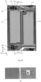
- FIG. 1 is a schematic plan view of an array substrate 500.
- the array substrate 500 includes a plurality of pixel unit groups 510 arranged in an array, gate lines 542 extending along a first direction D1, and data lines 561 extending along a second direction D2 intersecting with (e.g., perpendicular to) the first direction D1.
- One data line 561 is disposed between two pixel unit groups 510 that are adjacent in the first direction D1
- two gate lines 542 are disposed between two pixel unit groups 510 that are adjacent in the second direction D2.
- Each row of pixel unit groups 510 are driven by the two gate lines 542 on the two sides of the each row of the pixel unit groups 510 (that is, one gate line 542 on the upper side of the each row of pixel unit groups 510 and one gate line 542 on the lower side of the each row of pixel unit groups 510).
- each pixel unit group 510 includes a first pixel and a second pixel which are arranged side by side (arranged in parallel) and are immediately adjacent to each other in the first direction D1.
- the first pixel includes a first pixel electrode 521, a first switching element 523, and a first wire 522.
- the first wire 522 is used for connecting the first switching element 523 and the data line 561 for driving the first pixel.
- the second pixel includes a second pixel electrode 531, a second switching element 533 and a second wire 532.
- the second wire 532 is used for connecting the second switching element 533 and the data line 561 for driving the second pixel.
- the first pixel electrode 521 and the first switching element 523 are electrically connected through a first via-hole 524
- the second pixel electrode 531 and the second switching element 533 are electrically connected through a second via-hole 534.
- An orthographic projection of the first via-hole 524 on the first pixel electrode 521 at least partially overlaps with the first pixel electrode 521
- an orthographic projection of the second via-hole 534 on the second pixel electrode 531 at least partially overlaps with the second pixel electrode 531.
- the first switching element 523 and the second switching element 533 for driving the same pixel unit group 510 are arranged side by side in the second direction D2, and the first switching element 523 and the second switching element 533 at least partially overlap with each other in the second direction D2, that is, the orthographic projections of the first switching element 523 and the second switching element 533 on a plane perpendicular to the second direction D2 at least partially overlap with each other.
- the first wire 522 and the second wire 532 are disposed between two gate lines 542 which are between two pixel unit groups 510 that are adjacent in the second direction D2.
- a display panel including the array substrate 500 includes a black matrix (not shown), and an orthographic projection of the black matrix on the array substrate 500 covers the gate lines 542, the data lines 561, the first wires 522, the second wires 532, the first switching elements 523, the second switching elements 533, the first via-holes 524 and the second via-holes 534.
- the first wires 522, the second wires 532, and the data lines 561 are made of the same material.
- the inventors of the present disclosure have discovered in the research that the aperture ratio of the display panel including the array substrate as illustrated in FIG. 1 is low. Also, although the aperture ratio of the display panel including the array substrate as illustrated in FIG. 1 can be slightly increased by reducing the widths of the first and second wires in the second direction, reducing of the widths of the first and second wires in the second direction can increase the risks of disconnection of the first wires and disconnection of the second wires. In addition, signals on the first and second wires can interfere with signals on other wires of the array substrate.
- the array substrate includes a pixel unit group.
- the pixel unit group includes a first pixel and a second pixel arranged side by side and immediately adjacent to each other in a first direction;
- the first pixel includes a first pixel electrode, a first switching element, and a first connection portion extending and protruding from the first pixel electrode
- the second pixel includes a second pixel electrode, a second switching element, and a second connection portion extending and protruding from the second pixel electrode;
- the first pixel electrode and the first switching element are electrically connected to each other via the first connection portion, the second pixel electrode and the second switching elements are electrically connected to each other via the second connection portion; and an extension length of the first connection portion is not equal to an extension length of the second connection portion.
- the array substrate as well as the display panel and the display device including the array substrate has the capability to increase the aperture ratio or the basis for increasing the aperture ratio.
- the array substrate having the capability to increase the aperture ratio or the basis to increase the aperture ratio can have a display unevenness phenomenon (e.g., shaking stripe phenomenon, shaking stripe defect).
- the shaking stripe is a kind of bright and dark alternating stripes that can only be observed when a user of a display panel is shaking his head.
- the shaking stripes are related to different jump change values ⁇ Vp of pixel voltages for different pixels, and a factor that affects a jump change value ⁇ Vp of pixel voltage of a pixel includes: a lateral capacitance of the pixel, which includes a capacitance Cgs formed by a gate line and a source-drain layer, a capacitance Cpg formed by a pixel electrode and a gate line corresponding to the pixel electrode, and a capacitance Cpg' formed by a pixel electrode and a gate line adjacent to the pixel electrode (but not used to drive the pixel where the pixel electrode is located).
- a lateral capacitance of the pixel which includes a capacitance Cgs formed by a gate line and a source-drain layer, a capacitance Cpg formed by a pixel electrode and a gate line corresponding to the pixel electrode, and a capacitance Cpg' formed by a pixel electrode and a gate line adjacent to the pixel electrode
- the long connection pixel has the jump change value ⁇ Vp of pixel voltage more approximate to the jump change value ⁇ Vp of pixel voltage of the short connection pixel, and thus the shaking stripe phenomenon can be alleviated.
- the definition, causes, related factors, and experimental methods for observing and studying shaking stripes will be described in detail later, which will not be elaborated here.
- a portion of a gate line (the first gate line and the second gate line) corresponding to each pixel (the first pixel and the second pixel) have an orthographic projection on the source-drain layer overlapping with one of two source-drain electrodes of the pixel in at least two separated positions, it is possible to reduce a variation range (a range deviating from the design value) of the capacitance Cgs formed by the gate line and the source-drain layer, and thus it can mitigate the display unevenness phenomenon (e.g., shaking stripe phenomenon, shaking stripe defect).
- an overlapping area between an orthographic projection of the first gate line on the source-drain layer and one of two first source-drain electrodes equal to an overlapping area between an orthographic projection of the second gate line on the source-drain layer and one of two second source-drain electrodes, it is possible to make the capacitance Cgs of the long connection pixel equal to the capacitance Cgs of the short connection pixel, and thus it can further mitigate, for example, shaking stripe phenomenon, shaking stripe defect.
- a lateral distance between the first pixel electrode and the gate line driving the first pixel larger than five microns, it is possible to reduce the influence of the following factors on the capacitance Cpg of the first pixel: a variation (e.g., a variation due to manufacturing processes) of the lateral distance between the first pixel electrode and the gate line for driving the first pixel; variation in the effective overlapping length between the gate line for driving the first pixel and the combined structure of the first pixel electrode and the first connection portion.
- a variation e.g., a variation due to manufacturing processes
- a lateral distance between the second pixel electrode and the gate line driving the second pixel By making a lateral distance between the second pixel electrode and the gate line driving the second pixel larger than five microns, it is possible to reduce the influence of the following factors on the capacitance Cpg of the second pixel: a variation of the lateral distance between the second pixel electrode and the gate line for driving the second pixel; variation in the effective overlapping length between the gate line for driving the second pixel and the combined structure of the second pixel electrode with the second connection portion. Therefore, the requirement for the manufacturing process can be reduced without degrading the display evenness.
- the side, which is closer to the gate line for driving the long connection pixel, of the pixel electrode of the long connection pixel have a recessed portion, it is possible to shorten the effective overlapping length lpg between the gate line and the combined structure of the pixel electrode and the connection portion of the long connection pixel.
- the effective overlapping length between a gate line and the combined structure of the pixel electrode and the connection portion of the long connection pixel can be more approximate to the effective overlapping length between a gate line and the combined structure of the pixel electrode and the connection portion of the short connection pixel, and thus the capacitance Cpg of long connection pixel can be more approximate to the capacitance Cpg of the short connection pixel, thereby further mitigating the shaking stripe defect.
- Non-limitative descriptions are given to the array substrate provided by at least an embodiment of the present disclosure in the following with reference to a plurality of examples or embodiments. As described in the following, in case of no conflict, different features in these specific examples or embodiments may be combined so as to obtain new examples or embodiments, and the new examples or embodiments are also fall within the scope of present disclosure.
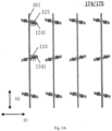
- FIG. 2A is a schematic plan view of an array substrate 100 provided by at least one embodiment of the present disclosure.
- the array substrate 100 includes a plurality of pixel unit groups 110 arranged in an array, a plurality of first gate lines 141, a plurality of second gate lines 142 and a plurality of data lines 161.
- the plurality of first gate lines 141 and the plurality of second gate lines 142 extend substantially along the first direction D1, respectively, and the plurality of data lines 161 extend substantially along the second direction D2 intersecting with (e.g., perpendicular to) the first direction D1.
- Each row of pixel unit groups 110 are driven by two gate lines, and the two gate lines (one first gate line 141 and one second gate line 142) are located on the two sides of the each row of pixel unit groups 110 in the second direction D2 and immediately adjacent to the each row of pixel unit groups 110.
- the gate line being immediately adjacent to a pixel unit group 110 refers to that no other gate line is disposed between the above pixel unit group 110 and the above gate line.
- Two gate lines are disposed between two pixel unit groups 110 that are adjacent in the second direction D2, and one data line is disposed between two pixel unit groups 110 that are adjacent in the first direction D1.
- FIG. 2B is a schematic plan view of a pixel unit group 110 of the array substrate 100 as illustrated in FIG. 2A .
- FIG. 2B also illustrates the first gate line 141, the second gate line 142, and the data line 161.
- Part or all of the pixel unit groups 110 of the array substrate 100 as illustrated in FIG. 2A can be implemented as the pixel unit group 110 illustrated in FIG. 2B .
- the pixel unit group 110 includes a first pixel and a second pixel that are arranged side by side and immediately adjacent to each other in the first direction D1. It should be noted that the first pixel and the second pixel being arranged side by side and immediately adjacent to each other refers to that no other pixel is provided between the above first pixel and the above second pixel.
- the first pixel includes a first pixel electrode 121, a first switching element 123, and a first connection portion 122 extending and protruding from the first pixel electrode 121
- the second pixel includes a second pixel electrode 131, a second switching element 133 and a second connection portion 132 extending and protruding from the second pixel electrode 131.
- the first pixel electrode 121 and the first switching element 123 are electrically connected to each other via the first connection portion 122
- the second pixel electrode 131 and the second switching element 133 are electrically connected to each other via the second connection portion 132.
- the extension length of the first connection portion 122 is not equal to (e.g., smaller than) the extension length of the second connection portion 132.
- the first pixel when the extension length of the first connection portion 122 is smaller than the extension length of the second connection portion 132, the first pixel can also be referred to as a short connection pixel, and the second pixel can also be referred to as a long connection pixel.
- the pixel, which has a connection portion of a smaller extension length, of each pixel unit group is referred to as a short connection pixel
- the pixel included in each pixel unit group which has a connection portion of a larger extension length is referred to as a long connection pixel.
- all short connection pixels of the array substrate are referred to as first pixels
- all long connection pixels of the array substrate are referred to as second pixels.
- the extension length of the first connection portion 122 be not equal to (e.g., smaller than) the extension length of the second connection portion 132, it is possible to provide both of the first switching element 123 and the second switching element 133 on an edge of the pixel unit group 110 in the first direction D1.
- the following is an exemplary description with reference to FIG. 2B .
- the pixel unit group 110 includes a first edge 111 and a second edge 112 which are opposite to each other in the first direction D1, and both of the first switching element 123 and the second switching element 133 are closer to the first edge 111 of the pixel unit group 110 than to the second edge 112.
- the first switching element 123 and the second switching element 133 of each pixel unit group 110 are connected to the same data line 161.
- the distance between the first switching element 123 of each pixel unit group 110 and the same data line 161 is the same as the distance between the second switching element 133 of each pixel unit group 110 and the same data line 161.
- a connection line between the first switching element 123 of each pixel unit group 110 and the data line 161 for driving the pixel unit group 110 can have a length (the length in the first direction D1) equal to a length (the length in the first direction D1) of a connection line between the second switching element 133 of each pixel unit group 110 and the data line 161 for driving the pixel unit group 110.
- the switching elements connected to the same data line 161 include a switching element disposed on the first side (e.g., the left side) of the same data line 161 and a switching element disposed on the second side (e.g., the right side) of the same data line 161, and the switching element on the first side (e.g., the left side) of the same data line 161 and the switching element on the second side (e.g., the right side) of the same data line 161 partially overlap in the first direction D1.
- a structure A and a structure B overlap (or partially overlap) in a direction C refers to that an orthographical projection of the structure A on a plane D perpendicular to the direction C overlaps (or partially overlaps) with an orthographical projection of the structure B on the plane D.
- the switching element on the first side (e.g., left side) of the same data line 161 and the switching element on the second side (e.g., right side) of the same data line 161 partially overlap in the first direction D1
- the first connection portion 122 and the second connection portion 132 of the pixel unit group 110 are respectively disposed on two sides of the first pixel electrode 121 in the second direction D2.
- the first connection portion 122 and the second connection portion 132 are both disposed between the first gate line 141 and the second gate line 142 in the second direction D2.
- the first connection portion 122 extends and protrudes in the second direction D2, and the second connection portion 132 extends and protrudes in the first direction D1.
- the extension length of the first connection portion 122 refers to the length of the first connection portion 122 in the second direction D2; the extension length of the second connection portion 132 refers to the length of the second connection portion 132 in the first direction D1 That is, the extension length of the connection portion refers to the length of the connection portion in the extending direction of the connection portion.
- the extension length of the connection portion can also be the overall length or physical length of the connection portion.
- the second connection portion 132 at least partially overlaps with the first pixel electrode 121.
- the first pixel electrode 121 is disposed between the first switching element 123 and the second switching element 133.
- first connection portion 122 and the first pixel electrode 121 are integrally formed by a same material
- second connection portion 132 and the second pixel electrode 131 are integrally formed by a same material
- the first switching element 123 and the second switching element 133 both closer to the same edge of the pixel unit group 110 (e.g., the first edge 111) in the first direction D1, forming the first connection portion 122 integrally with the first pixel electrode 121 by a same material, and forming the second connection portion 132 integrally with the second pixel electrode 131 by a same material, it is possible to make the first connection portion 122 (the first end 1221 of the first connection portion 122, see also FIG. 6 below) be electrically connected to the first pixel electrode 121 directly, and make the second connection portion 132 (the first end 1321 of the second connection portion 132, see also FIG.
- the first connection portion 122 (the second end 1222 of the first connection portion 122) is electrically connected to the first switching element 123 through the first via-hole 1223
- the second connection portion 132 (the second end 1322 of the second connection portion 132) is electrically connected to the second switching element 133 through the second via-hole 1323
- the first via-hole 1223 is closer to the first switching element 123
- the second via-hole 1323 is closer to the second switching elements 133
- the areas that are closer to the first switching element 123 and the second switching element 133 are correspond to the area shielded by the black matrix, and therefore, the first via-hole 1223 and the second via-hole 1323 as illustrated in FIG. 2B do not reduce the aperture ratio of the pixel unit group 110 and the aperture ratio of the array substrate 100.
- both the first pixel electrode 121 and the second pixel electrode 131 may be made of a transparent conductive material.
- the transparent conductive material is indium tin oxide (ITO) or indium zinc oxide (IZO).
- ITO indium tin oxide
- IZO indium zinc oxide
- the first connection portion 122 and the second connection portion 132 may also be made of a transparent conductive material (e.g., ITO).
- the processing accuracy of transparent conductive materials is higher than the processing accuracy of metal materials, that is, the width of a wire of a transparent conductive material can be smaller than the width of a wire of a metal material.
- the size of the areas occupied by the first connection portion 122 and the second connection portion 132 can be reduced, and the size of the areas occupied by the first pixel electrode 121 and the second pixel electrode 131 can be correspondingly increased, thereby further increasing the aperture ratio of the pixel unit group 110 and aperture ratio of the array substrate 100.
- both the first switching element 123 and the second switching element 133 are U-shaped TFTs.
- the opening directions of the U-shaped TFTs in the pixel unit groups in adjacent rows are opposite.
- the opening direction of the U-type TFTs of the pixel unit groups in the first row is to the right
- the opening direction of the U-type TFTs in the pixel unit groups in the second row is to the left.
- the U-type TFTs of the pixel unit groups in the first row are disposed on the right side of a data line
- the U-type TFTs of the pixel unit groups in the second row are disposed on the left side of a data line.
- the inventors of the present disclosure have discovered in their research that although it is possible to increase the aperture ratio of the array substrate by making the pixel unit group of the array substrate as illustrated in FIG. 2A include long connection pixels and short connection pixels, it can also lead to a phenomenon of uneven brightness of the array substrate (e.g., shaking stripe phenomenon, shaking stripe defect) as illustrated in FIG. 2A .
- a phenomenon of uneven brightness of the array substrate e.g., shaking stripe phenomenon, shaking stripe defect
- FIGS. 2C-2H The issues related to the shaking stripe defect will be described in detail below with reference to FIGS. 2C-2H .
- the shaking stripes are a kind of bright and dark alternating stripes that can only be observed when a user of a display panel is shaking his head.
- the left image of FIG. 2C is an image observed when the user of the display panel is not shaking his head
- the right image of FIG. 2C is an image observed when the user of the display panel is shaking his head (that is, an image with shaking stripes).
- the display panel is configured to display an image with a gray scale of 127 (that is, the gray scale of each pixel of the image is 127).
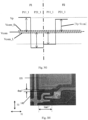
- FIG. 2D illustrates a schematic diagram of an exemplary calculation method of a spatial frequency.
- the spatial frequency fs refers to the number of the grid cycles of the brightness and darkness, that is sinusoidal modulated, of the image (or stimulus pattern) per degree of viewing angle, or the number of cycles of the image bright and dark distribution per degree of viewing angle.
- the unit of the spatial frequency fs is cycles/degree, and the spatial frequency fs can be expressed by formula (1), and the optimal observation distance of the shaking stripe phenomenon can be expressed by formula (2).
- r is an observation distance, that is, a distance from the user's eye 611 to the display panel 612; 1 is a width (width in the row direction) of the sub-pixel of the display panel; n is the number of (the amount of) pixels in a bright and dark cycle, ⁇ is a viewing angle, and d ⁇ is a viewing angle per degree.
- FIG. 2E illustrates the optimal observation distance of the shaking stripes of display panels of different types. As illustrated in FIG. 2E , the optimal observation distance of the shaking stripes of most display panels is between 0.2 meter and 0.5 meter. It should be noted that "rim” as illustrated in FIG. 2E indicates that the ordinate in FIG. 2E represents the observation distance r, and the unit of the observation distance r is "meter”; and "HD", “FHD”, and “UHD” respectively indicate "High Definition”, “Full HD” and "Ultra High Definition”.
- Fig. 2F illustrates reasons for causing the occurrence of the shaking stripe defect.
- the display panel displays a first frame of image F1, a second frame of image F2, a third frame of image F3, a fourth frame of image F4, a fifth frame of image F5, a sixth frame of image F6, a seventh frame of image F7, and an eighth frame of image F8.
- the image seen by the human eye is an image obtained by superimposing and averaging a plurality of images adjacent in time, the user cannot observe the shaking stripe phenomenon while the user's head remains stationary.
- the user's head moves (e.g., shaking his head)
- the user cannot observe part of the frames of images (e.g., the user does not observe the fourth frame of image F4- the sixth frame of image F6), and therefore, the user's eye cannot average the observed images well.
- the user can observe the shaking stripe phenomenon.
- the user's eyes cannot eliminate the difference in brightness between different pixels in the display image of the same frame by averaging the third frame of image F3 and the seventh frame of image F7 he has observed.
- the first pixel voltage applied to the pixel electrode is larger than the common voltage Vcom.
- the second pixel voltage applied to the pixel electrode is less than the common voltage Vcom, and the voltage difference between the first pixel voltage and the common voltage Vcom is smaller than the voltage difference between the common voltage Vcom and the second pixel voltage, that is, the brightness of the second frame of image F2, the fourth frame of image F4, the sixth frame of image F6, and the eighth frame of image F8 is larger than that of the first frame of image F1, the third frame of image F3, the fifth frame of image F5, and the seventh frame of image F7.
- FIG. 2G is a schematic diagram illustrating charging and discharging pixels of the display panel.
- FIG. 2G illustrates profiles of a drain voltage Vd, a common voltage Vcom, a pixel voltage Vp, and a gate voltage Vg of a pixel of the display panel over time.
- each display cycle of a pixel may include a first display frame F1 and a second display frame F2 adjacent to each other.
- the second display frame F2 is, for example, an inverted display frame.
- the polarity of the voltage on the pixel electrode of each pixel of the array substrate is opposite to that of the first display frame F1.
- the first display frame F1 and the second display frame F2 each include a voltage writing phase Tw and a voltage holding phase Th.
- ⁇ Vp is the jump change value in the absolute value of the difference between the drain voltage Vd and the common voltage Vcom.
- ⁇ Vp is also referred to as the jump change value of pixel voltage.
- Vh is the holding voltage.
- the inventors of the present disclosure have discovered in their research that, without considering the voltage holding rate (VHR), the jump change value ⁇ Vp of the pixel voltage significantly affects the brightness difference between adjacent display frames and the brightness evenness of the same display frame (e.g., the shaking stripe phenomenon), especially for the display panel of a dual-gate structure, this is because that the structure of adjacent sub-pixels of the display panel of the dual-gate structure can be different, exemplary description will be provided below with reference to FIG. 2H .
- VHR voltage holding rate
- FIG. 2H illustrates a schematic diagram of capacitances related to pixels of the display panel.
- the capacitances related to pixels include a capacitance Cgs, a capacitance Cpg, a capacitance Cpg', a capacitance Cpd, a capacitance Cpd', a capacitance Cst, and a capacitance Clc.
- the jump change value ⁇ Vp of the pixel voltage can be expressed by the following formula (3).
- ⁇ V p Cgs + Cpg + Cpg ′ Cst + Cgs + Cpg + Cpg ′ + Cpd + Cpd ′ ⁇ Vgh ⁇ Vgl
- the capacitance Cgs is a capacitance formed between one of the source electrode and the drain electrode of the switching element and the gate line (and/or gate electrode) for driving the switching element;
- the capacitance Cpg is a lateral capacitance formed between the pixel electrode and the gate line (and/or gate electrode) for driving the pixel where the pixel electrode is located;
- the capacitance Cpg' is a lateral capacitance formed between the pixel electrode and the gate line adjacent to the pixel electrode (not for driving the pixel where the pixel electrode is located);
- the capacitance Cpd is a lateral capacitance formed between the pixel electrode and the data line for driving the pixel where the pixel electrode is located;
- the capacitance Cpd' is a lateral capacitance formed between the pixel electrode and the data line adjacent to the pixel electrode (not for driving the pixel where the pixel electrode is located).
- the capacitance Cst and the capacitance Clc are storage capacitances of the pixel, COM is the common electrode; Vgh and Vgl respectively are the first level and the second level of the gate scanning signal received by the gate line.
- the voltage value at the first level is larger than the voltage value at the second level.
- GLn and GLn+1 are respectively the gate lines located in the n-th row and the (n+1)th row; DLn and DLn+1 are respectively the data lines located in the n-th column and the (n+1)th column.
- the inventors of the present disclosure have discovered in their research that the shaking stripes are related to the difference in brightness of different sub-pixels of the same frame of image (the theoretical gray scale of different sub-pixels are the same), and the difference in brightness of different sub-pixels of the same frame of image is related to the jump change values ⁇ Vp of the pixel voltages of the different sub-pixels.
- the inventors of the present disclosure have discovered in their research that the array substrate as illustrated in FIG. 2A can have a problem of uneven brightness (e.g., the shaking stripe problem) due to at least one of the following reasons: (1) the source-drain metal layer of the array substrate is offset relative to the gate metal layer; (2) the capacitance Cpg of the long connection pixels of the array substrate is not equal to the capacitance Cpg of the short connection pixels of the array substrate; (3) the capacitance Cpg' of the long connection pixels of the array substrate is not equal to the capacitance Cpg' of the short connection pixels of the array substrate.
- uneven brightness e.g., the shaking stripe problem
- the following is an exemplary description of brightness unevenness that is caused by the offset between the source-drain metal layer and the gate metal layer of the array substrate with reference to FIGS. 3A-3C .
- FIG. 3A is a schematic diagram of the array substrate as illustrated in FIG. 2A ;
- FIG. 3B is an enlarged view of an area RC1 of the array substrate as illustrated in FIG. 2A
- FIG. 3C is an enlarged view of an area RC2 of the array substrate as illustrated in FIG. 2A .
- FIG. 3A illustrates a plurality of first gate lines, a plurality of second gate lines, a plurality of data lines, and pixel unit groups arranged in an array.
- the plurality of first gate lines includes a gate line GL1_1, a gate line GL2_1, a gate line GL3_1, and a gate line GL4_1.
- the plurality of second gate lines includes a gate line GL1_2, a gate line GL2 2, a gate line GL3_2, and a gate line GL4_2.
- the plurality of data lines includes data lines DL1-DL7.
- the pixel unit groups arranged in the array include, for example, a pixel P11_1, a pixel P11_2, a pixel P12_1, a pixel P12_2, a pixel P21_1, a pixel P21_2, a pixel P22_1, and a pixel P22_2.
- FIG. 3B is an enlarged view of the area RC1 of the array substrate as illustrated in FIG. 2A , that is, FIG. 3B illustrates an overlapping area 201 between one of the source electrode and the drain electrode of the switching element of the pixel P11_2 and a gate line (and/or a gate electrode) for driving the switching element.
- FIG. 3C is an enlarged view of the area RC2 of the array substrate as illustrated in FIG. 2A , that is, FIG. 3C illustrates an overlapping area 202 between one of the source electrode and the drain electrode of the switching element of the pixel P11_1 and a gate line (and/or a gate electrode) for driving the switching element.
- the opening direction of the U-shaped electrodes of the switching elements of the pixel P12_1 and the pixel P12_2 (that is, the other of the source electrode and the drain electrode of the switching element) is the same as the opening direction of the U-shaped electrodes of the switching elements of the pixel P11_1 and the pixel P11_2, when the source electrode and the drain electrode of the switching element move to the right relative to the gate electrode of the switching element, the capacitance Cgs of the pixel P12 2 and the pixel P12_1 and the jump change value ⁇ Vp of the pixel voltage also decrease.
- the opening directions of the U-shaped electrodes of the switching elements of the pixels P21_1, P21_2, P22_1, and P22_2 are opposite to the opening directions of the U-shaped electrodes of the switching elements of the pixels P11_1 and P11_2, when the source electrode and the drain electrode of the switching element move to the right relative to the gate electrode of the switching element, the capacitance Cgs of the pixels P21_1, P21_2, P22_1, and P22_2, and the jump change value ⁇ Vp of the pixel voltage are all increased.
- the pixel P11_1 and the pixel P11_2 are both connected to the data line DL1 in the first column, the pixel P12_1, the pixel P12_2, the pixel P21_1, the pixel P21_2 are all connected to the data line DL2 in the second column, the pixel P22_1 and the pixel P22_2 are both connected to the data line DL3 in the third column; the polarities of the voltages applied to the data line DL1 and the data line DL2 are opposite, and the polarities of the voltages applied to the data line DL1 and the data line DL3 are the same.
- the voltages applied to the data line DL1, the data line DL2, and the data line DL3 are positive voltage, negative voltage, and positive voltage, respectively (pixel P11_1, pixel P11_2, pixel P22_1, and pixel P222 are in the positive display frame pixel P12_1, pixel P12_2, pixel P21_1, and pixel P21 2 are all in a negative display frame) and the brightness of a pixel is negatively correlated with the absolute value of the difference between the pixel voltage and the common voltage of the pixel, the brightness of the pixels in the pixel unit groups in the odd-numbered columns is low, and the brightness of the pixels in the pixel unit groups in the even-numbered columns is high.
- a pixel in a positive display frame refers to that the voltage on the pixel electrode of the pixel is a positive voltage
- a pixel in a negative display frame refers to that the voltage on the pixel electrode of the pixel is a negative voltage
- FIG. 3D is a schematic diagram of pixel voltages of pixels in pixel unit groups in odd-numbered columns when the source-drain metal layer is not offset (dashed line) and offset (solid line) relative to the gate metal layer
- FIG. 3E is a schematic diagram of pixel voltages of pixels in pixel unit groups in even-numbered columns when the source-drain metal layer is not offset (dashed line) and offset (solid line) relative to the gate metal layer.
- the image displayed on the display panel including the array substrate as illustrated in FIG. 2A can have a display unevenness problem (e.g., a shaking stripe problem).
- the parameters that affect the capacitance Cpg of the pixels includes a lateral distance dpg and an effective overlapping length lpg.
- FIG. 3F illustrates the lateral distance dpg1 and the effective overlapping length lpg1 between the combined structure of the pixel electrode an the connection portion of the short connection pixel (first pixel, P11_1) and the gate line for driving the short connection pixel
- FIG. 3F also illustrates the lateral distance dpg1 and the effective overlapping length lpg1 between the combined structure of the pixel electrode and the connection portion of the long connection pixel (second pixel, P11_1) and the gate line for driving the long connection pixel.
- the lateral distance dpg of a pixel refers to a distance between the pixel electrode of the pixel (the pixel electrode which is close to the edge of the gate line for driving the pixel) and the gate line for driving the pixel (the gate line close to the edge of the pixel electrode).
- the capacitance Cpg of the short connection pixel is smaller than the capacitance Cpg of the long connection pixel. Therefore, the jump change value of the pixel voltage of the short connection pixel is ⁇ Vp is smaller than the jump change value ⁇ Vp of the pixel voltage of the long connection pixel.
- FIG. 3G is a schematic diagram illustrating the comparison of the pixel voltages of the short connection pixel P11_1 and the long connection pixel P21_1 in a positive display frame and a negative display frame.
- the short connection pixel P11_1 in the first image frame F1, the short connection pixel P11_1 is in a positive display frame, and the long connection pixel P21_1 is in a negative display frame; in the second image frame F2, the short connection pixel P11_1 is in a negative display frame, and the long connection pixel P21_1 is in the positive display frame.
- both of the short connection pixel P11_1 and the long connection pixel P21_1 are slightly darker.
- the short connection pixel P11_1 and the long connection pixel P21_1 are both slightly brighter.
- the pixel voltage Vp of the short connection pixel P11_1 in the positive display frame increases, and the absolute value of the difference between the pixel voltage Vp and the common voltage Vcom
- the other pixels located in the column where the short connection pixel P11_1 and the long connection pixel P21_1 are located are also slightly darker.
- all pixels located in the column where the long connection pixel P11_2 and the short connection pixel P21_2 are located are slightly brighter.
- the pixel voltage Vp of the short connection pixel P11_1 in the negative display frame increases, and the absolute value of the difference between the pixel voltage Vp and the common voltage Vcom
- the other pixels located in the column where the short connection pixel P11_1 and the long connection pixel P21_1 are located are also slightly brighter.
- all pixels located in the column where the long connection pixel P11_2 and the short connection pixel P21_2 are located are slightly darker.
- the common voltage should be increased from Vcom to Vcom_S (the optimal common voltage for the short connection pixel P11_1); however, when only the long connection pixel P21_1 is considered, the common voltage should be decreased from Vcom to Vcom_L (the optimal common voltage for the long connection pixel P21_1). Therefore, it is difficult to adjust the common voltage to eliminate the uneven brightness of the image caused by the difference between the Cpg of the long connection pixel and the Cpg of the short connection pixel (all the pixels in the same column are brighter or darker in the same image frame).
- the parameters that affect the capacitance Cpg' of the pixel include the lateral distance dpg' and the effective overlapping length lpg'.
- FIG. 3H illustrates a schematic view of the area RC1 of the array substrate as illustrated in FIG. 2A (obtained by a scanning electron microscope)
- FIG. 3I illustrates a schematic view of the area RC3 of the array substrate as illustrated in FIG. 2A (obtained by a scanning electron microscope).
- the first pixel electrode 121 and the gate line adjacent to the first pixel electrode 121 overlap with each other in the second direction D2.
- the second pixel electrode 131 and the gate line adjacent to the second pixel electrode 131 overlap with each other in the second direction D2.
- the second pixel electrode 131 illustrated in FIG. 3I and the first pixel electrode 121 illustrated in FIG. 3H are located in two different pixel unit groups (two pixel unit groups that are adjacent in the second direction D2);
- the second pixel electrode 131, which is in the same pixel unit group as the first pixel electrode 121 as illustrated in FIG. 3H is located under the gate line that is adjacent to the second pixel electrode 131, and thus, before charging the pixel where the second pixel electrode 131, which is in the same pixel unit group as the first pixel electrode 121 illustrated in FIG.
- the scanning of the gate line that is adjacent to the second pixel electrode 131 has ended. Therefore, the charging process of the second pixel electrode 131, which is in the same pixel unit group as the first pixel electrode 121 illustrated in FIG. 3H , is not affected by (or the influence is very small) the gate line that is adjacent to the second pixel electrode 131.
- the distance between the first pixel electrode 121 and the gate line (e.g., the second gate line 142) adjacent to the first pixel electrode 121 in the second direction D2 can be used as the lateral distance dpg1'
- the distance between the second pixel electrode 131 and the gate line (e.g., the second gate line 142) adjacent to the second pixel electrode 131 in the second direction D2 can be used as the lateral distance dpg2'.
- the effective overlapping length lpg1' between the first pixel electrode 121 and the gate line adjacent to the first pixel electrode 121 refers to a length in the first direction D 1 of a region of the gate line adjacent to the first pixel electrode 121, in which the region of which corresponds to an area where the lateral distance is less than or equal to a predetermined distance (e.g., less than or equal to the lateral distance dpg1'); and the effective overlapping length lpg2' between the second pixel electrode 131 and the gate line adjacent to the second pixel electrode 131 refers to a length in the first direction D1 of a region of the gate line adjacent to the second pixel electrode 131, in which the region of which corresponds to an area where the lateral distance is less than or equal to a predetermined distance (e.g., less than or equal to the lateral distance dpg2').
- the array substrate when an array substrate adopts a GOA (Gate Drive on Array) to drive the gate lines, the array substrate has a pre-charging function, and the capacitance Cpg' can cause pixel voltage of pixels (e.g., pixels driven by odd-numbered rows of gate lines) further decrease, exemplary description will be given below with reference to FIG. 3J .
- GOA Gate Drive on Array
- Fig. 3J is a schematic diagram illustrating the effect of the capacitor Cpg' on the pixel voltage Vp.
- Vgate1 is a gate line in an odd-numbered row
- Vgate2 is a gate line in an even-numbered row
- Vp is a pixel voltage of a pixels in an even-numbered row.
- the pixel voltage Vp of the pixel has an additional increment due to the influence of the capacitance Cpg', but because the pixel is at the charging stage at this time, the above additional increments will be removed.
- FIG. 3J is a schematic diagram illustrating the effect of the capacitor Cpg' on the pixel voltage Vp.
- the inventors of the present disclosure have discovered in research that when the capacitance Cgs of the long connection pixel and the capacitance Cgs of the short connection pixel are more approximate to each other and/or the capacitance Cpg of the long connection pixel and the capacitance Cpg of the short connection pixel are more approximate to each other, the jump change value of pixel voltage ⁇ Vp of the long connection pixel is more approximate to the jump change value of pixel voltage ⁇ Vp of the short connection pixel, thereby reducing the display unevenness phenomenon (e.g., the shaking stripe phenomenon).
- FIG. 4A The following is an exemplary description with reference to FIG. 4A .
- FIG. 4A is a schematic plan view of another array substrate 100 provided by at least one embodiment of the present disclosure.
- the array substrate 100 as illustrated in FIG. 4A differs from the array substrate as illustrated in FIG. 2A in that: (1) the array substrate 100 as illustrated in FIG. 4A has Cgs compensation capability; (2) the pixel electrode of the long connection pixel of the array substrate 100 as illustrated in FIG. 4A has a recessed portion on the side closer to the gate line for driving the long connection pixel; (3) the array substrate 100 as illustrated in FIG. 4A has first and second via-holes different from the first and second via-holes of the array substrate 100 as illustrated in FIG. 2A ; and ( 4 ) the array substrate 100 as illustrated in FIG. 4A has a common electrode pattern different from the common electrode pattern of the array substrate 100 as illustrated in FIG. 2A .
- FIG. 4A Exemplary description of the array substrate 100 as illustrated in FIG. 4A will be given below with reference to FIGS. 4A-4E , 5A-5H and 6-11 .
- the array substrate 100 includes a plurality of pixel unit groups 110 arranged in an array, a plurality of first gate lines 141, a plurality of second gate lines 142, and a plurality of data lines 161.
- the plurality of first gate lines 141 and the plurality of second gate lines 142 extend substantially in the first direction D1, respectively, and the plurality of data lines 161 substantially extend in the second direction D2 intersecting with (e.g., perpendicular to) the first direction D1.
- Each row of pixel unit groups 110 is driven by two gate lines, and the two gate lines (one first gate line 141 and one second gate line 142) are disposed on two sides of the each row of pixel unit groups 110 in the second direction D2 and are immediately adjacent to the each row pixel unit groups 110.
- the gate line being immediately adjacent to the pixel unit groups 110 refers to that no other gate line is disposed between the pixel unit groups 110 and the above gate line.
- Two gate lines are provided between two pixel unit groups 110 that are adjacent in the second direction D2, and one data line is provided between two pixel unit groups 110 that are adjacent in the first direction D1. The following is an exemplary description with reference to FIG. 4A .
- each row of pixel unit groups 110 corresponds to one of the plurality of first gate lines 141 and one of the plurality of second gate lines 142, and the one of the plurality of first gate lines 141 and the one of the plurality of second gate lines 142 are disposed on two sides of the each row of pixel unit groups 110 in the second direction D2, and are configured to drive the each row of pixel unit groups 110.
- one first gate line 141 and one second gate line 142 are disposed between adjacent pixel unit groups 110 in the column direction (that is, the second direction D2).
- the one gate line 141 and the one second gate line 142 are respectively used to drive the pixel unit groups 110 of two adjacent rows.
- the plurality of first gate lines 141 and the plurality of second gate lines 142 are configured to drive corresponding pixel unit groups 110 adjacent to the plurality of first gate lines 141 and the plurality of second gate lines 142 (that is, there is no other gate line between the gate line and the pixel unit group 110 driven by the gate line).
- FIG. 4A one first gate line 141 and one second gate line 142 are disposed between adjacent pixel unit groups 110 in the column direction (that is, the second direction D2).
- the one gate line 141 and the one second gate line 142 are respectively used to drive the pixel unit groups 110 of two adjacent rows.
- the plurality of first gate lines 141 and the plurality of second gate lines 142 are configured to drive corresponding pixel unit groups 110
- one data line 161 is disposed between pixel unit groups 110 that adjacent in the row direction (that is, the first direction D1). As illustrated in FIG. 4A , the plurality of first gate lines 141 and the plurality of second gate lines 142 are alternately arranged in the second direction D2.
- the expression that the plurality of first gate lines 141 and the plurality of second gate lines 142 extending substantially along the first direction D1, respectively, only defines the extending direction of the lengths of the first gate lines 141 and the second gate lines 142, and it does not mean that the first gate line 141 and the second gate line 142 are parallel to the first direction D1. That is, according to actual application requirements, the first gate line 141 and the second gate line 142 can be parallel to the first direction D1 or part of the first gate line 141 and part of the second gate line 142 may be not parallel to the first direction D1.
- partial sections of the plurality of first gate lines 141 and the plurality of second gate lines 142 can be designed in a bent form.
- the data line 161 can be parallel to the second direction D2 or part of the data line 161 may not be parallel to the second direction D2.
- one pixel unit group 110 of the plurality of pixel unit groups 110 is made to one pixel unit group 110 of the plurality of pixel unit groups 110 as an example.
- FIG. 4B is a schematic plan view of the pixel unit group 110 of the array substrate 100 as illustrated in FIG. 4A .
- FIG. 4B also illustrates a first gate line 141, a second gate line 142, and a data line 161.
- Part or all of the pixel unit groups 110 of the array substrate 100 as illustrated in FIG. 4A can be implemented as the pixel unit group 110 illustrated in FIG. 4B .
- the pixel unit group 110 includes a first pixel and a second pixel that are arranged side by side and immediately adjacent to each other in the first direction D1. It should be noted that the first pixel and the second pixel being arranged side by side and immediately adjacent to each other refers to that no other pixel is provided between the first pixel and the second pixel.
- the first pixel includes a first pixel electrode 121, a first switching element 123, and a first connection portion 122 extending and protruding from the first pixel electrode 121
- the second pixel includes a second pixel electrode 131, a second switching element 133 and a second connection portion 132 extending and protruding from the second pixel electrode 131.
- the first pixel electrode 121 and the first switching element 123 are electrically connected to each other via the first connection portion 122
- the second pixel electrode 131 and the second switching element 133 are electrically connected to each other via the second connection portion 132.
- the extension length of the first connection portion 122 is not equal to (e.g., smaller than) the extension length of the second connection portion 132.
- the extension length of the first connection portion 122 is not equal to (e.g., smaller than) the extension length of the second connection portion 132, it is possible to provide both of the first switching element 123 and the second switching element 133 on an edge of the pixel unit group 110 in the first direction D1.
- the following is an exemplary description with reference to FIG. 4B .
- the pixel unit group 110 includes a first edge 111 and a second edge 112 opposite to each other in the first direction D1, and both of the first switching element 123 and the second switching element 133 are closer to the first edge 111 of the pixel unit group 110 than to the second edge 112.
- the first switching element 123 and the second switching element 133 of each pixel unit group 110 are connected to the same data line 161.
- the distance between the first switching element 123 of each pixel unit group 110 and the same data line 161 is the same as the distance between the second switching element 133 of each pixel unit group 110 and the same data line 161.
- a connection line between the first switching element 123 of each pixel unit group 110 and the data line 161 for driving the pixel unit group 110 can have a length (the length in the first direction D1) equal to a length (the length in the first direction D1) of a connection line between the second switching element 133 of each pixel unit group 110 and the data line 161 for driving the pixel unit group 110.
- the switching elements connected to the same data line 161 include a switching element disposed on the first side (e.g., the left side) of the same data line 161 and a switching element disposed on the second side (e.g., the right side) of the same data line 161, and the switching element on the first side (e.g., the left side) of the same data line 161 and the switching element on the second side (e.g., the right side) of the same data line 161 partially overlap in the first direction D1.
- the switching element on the first side (e.g., left side) of the same data line 161 and the switching element on the second side (e.g., right side) of the same data line 161 partially overlap in the first direction D1
- the first connection portion 122 and the second connection portion 132 of the pixel unit group 110 are respectively disposed on two sides of the first pixel electrode 121 in the second direction D2.
- the first connection portion 122 and the second connection portion 132 are both disposed between the first gate line 141 and the second gate line 142 in the second direction D2.
- the first connection portion 122 extends and protrudes in the second direction D2, and the second connection portion 132 extends and protrudes in the first direction D1.
- the second connection portion 132 at least partially overlaps with the first pixel electrode 121.
- the first pixel electrode 121 is disposed between the first switching element 123 and the second switching element 133.
- the first switching element 123 and the second switching element 133 are symmetrical with respect to the center line of the first pixel electrode 121 (or of the pixel unit group 110) in the second direction D2 which extends along the first direction D1 (see also FIG. 4D below).
- first connection portion 122 and the first pixel electrode 121 are integrally formed and made of a same material
- second connection portion 132 and the second pixel electrode 131 are integrally formed and made of a same material
- first connection portion 122, the first pixel electrode 121, the second connection portion 132, and the second pixel electrode 131 can be formed by patterning the same film layer through the same patterning process.
- the first switching element 123 and the second switching element 133 both closer to the same edge of the pixel unit group 110 (e.g., the first edge 111) in the first direction D1, forming the first connection portion 122 integrally with the first pixel electrode 121 by a same material, and forming the second connection portion 132 integrally with the second pixel electrode 131 by a same material, it is possible to make the first connection portion 122 (the first end 1221 of the first connection portion 122, see also FIG. 6 below) electrically connected to the first pixel electrode 121 directly, and make the second connection portion 132 (the first end 1321 of the second connection portion 132, see also FIG.
- the first connection portion 122 (the second end 1222 of the first connection portion 122) is electrically connected to the first switching element 123 through the first via-hole 1223
- the second connection portion 132 (the second end 1322 of the second connection portion 132) is electrically connected to the second switching element 133 through the second via-hole 1323
- the first via-hole 1223 is closer to the first switching element 123
- the second via-hole 1323 is closer to the second switching elements 133
- the areas closer to the first switching element 123 and the second switching element 133 correspond to the area shield by a black matrix, and therefore, the first via-hole 1223 and the second via-hole 1323 as illustrated in FIG. 4B does not reduce the aperture ratio of the pixel unit group 110 and the aperture ratio of the array substrate 100.
- both the first pixel electrode 121 and the second pixel electrode 131 can be made of a transparent conductive material.
- the transparent conductive material is indium tin oxide (ITO) or indium zinc oxide (IZO).
- ITO indium tin oxide
- IZO indium zinc oxide
- the first connection portion 122 and the second connection portion 132 can also be made of a transparent conductive material (e.g., ITO).
- the processing accuracy of a transparent conductive material is higher than the processing accuracy of a metal material, that is, the width of the wire of a transparent conductive material can be smaller than the width of the wire of a metal material.
- the size of the areas occupied by the first connection portion 122 and the second connection portion 132 can be reduced, and the size of the areas occupied by the first pixel electrode 121 and the second pixel electrode 131 can be correspondingly increased, thereby increasing the aperture ratio of the pixel unit group 110 and aperture ratio of the array substrate 100.
- switching elements connected to the same data line and located on the right side of the same data line are used to drive pixel unit groups of odd-numbered rows (or even-numbered rows); and switching elements connected to the same data line and located on the left side of the same data line are used to drive pixel unit groups of even-numbered rows (or odd-numbered rows)
- the first switching element 123 and the second switching element 133 for driving each pixel unit group are both disposed on the edge of the pixel unit group where the short connection pixel are provided in the first direction.
- the first switching element 123 and the second switching element 133 of the pixel unit group located in the odd-numbered row (or even-numbered row) are both disposed on the left side of the pixel unit group and the first switching element 123 and the second switching element 133 of the pixel unit group located in the even-numbered row (or odd-numbered row) are both disposed on the right side of the pixel unit group.
- both the first switching element 123 and the second switching element 133 are thin film transistors (TFTs).
- TFTs thin film transistors
- the first switching element 123 and the second switching element 133 are both U-shaped thin film transistors, that is, the source electrode (or drain electrode) of the thin film transistor is a U-shaped electrode, and at least part of the drain electrode (or source electrode) is disposed in the opening of the U-shaped electrode; and the source electrode and drain electrode of the U-shaped thin film transistor at least partially overlap in the second direction D2.
- the opening directions of U-shaped TFTs for driving adjacent rows are opposite.
- the opening direction of the U-type TFT for driving the first row is to the right
- the opening direction of the U-type TFT for driving the second row is to the left.
- the array substrate 100 can include a first electrode layer 172 (see FIG. 4C ), a first insulating layer 173 (see FIG. 5C ), a semiconductor layer 174 (see FIGS. 5A and 5C ), a second electrode layer 175 (see FIG. 5A ), a second insulating layer 176 (see FIG. 5C ) and a third electrode layer 177 (see FIG. 6 ).
- the first electrode layer 172, the first insulating layer 173, the semiconductor layer 174, the second electrode layer 175, the second insulating layer 176 and the third electrode layer 177 are sequentially disposed on the base substrate 171, for example.
- FIG. 4C is a schematic plan view of the first electrode layer 172 of the array substrate as illustrated in FIG. 4A .
- the first electrode layer 172 includes a plurality of first gate lines 141, a plurality of second gate lines 142, and a common electrode pattern 150 arranged in an array.
- the plurality of first gate lines 141 and the plurality of second gates lines 142 are alternately arranged in the second direction D2.
- the plurality of common electrode patterns 150 are in a one-to-one correspondence with the plurality of pixel unit groups 110.
- a plurality of common electrode patterns 150 of the same row are disposed between the first gate line 141 and the second gate line 142 which are used for driving the pixel unit groups 110 corresponding to the electrode patterns 150.
- the first electrode layer 172 does not include the common electrode patterns.
- FIG. 4D illustrates a schematic plan view of a first gate line 141 and a second gate line 142 of the array substrate as illustrated in FIG. 4A .
- the first gate line 141 for driving a pixel unit group 110 and the second gate lines 142 for driving a pixel unit group 110 adjacent to the above pixel unit group 110 in the second direction D2 partially overlap in the first direction D1. That is, the first gate lines 141 and the second gate lines 142 between pixel unit groups 110 that are adjacent in the second direction D2 partially overlap in the first direction D1, thereby reducing the size, in the second direction D2, of the area occupied by the gate lines, thereby improving the aperture ratio of the array substrate 100 and the aperture ratio of the display panel and display device including the array substrate 100.
- the first gate line 141 and the second gate line 142 are arranged symmetrically with respect to the center line 113, which extends in the first direction D1, of the pixel unit group 110 in the second direction D2.
- FIG. 4E illustrates a schematic plan view of a portion of the first gate line 141 and the second gate line 142 of the array substrate as illustrated in FIG. 4A corresponding to one pixel unit group 110.
- the first gate line 141 includes a first gate portion 1411
- the second gate line 142 includes a second gate portion 1421.
- the first gate portion 1411 is configured as the gate electrode of the first switching element 123
- the second gate portion 1421 is configured as the gate electrode of the second switching element 133.
- the orthographic projection of the U-shaped electrode (source electrode or drain electrode) of the first switching element 123 on the first electrode layer 172 at least partially overlaps with the first gate portion 1411
- the orthographic projection of the U-shaped electrode (source electrode or drain electrode) of the second switching element 133 on the first electrode layer 172 at least partially overlaps with the second gate portion 1421.
- the first gate portion 1411 of the gate line 141 for driving each pixel unit group 110 and the second gate portion 1421 of the second gate line 142 for driving the pixel unit group 110 that is adjacent to the each pixel unit group 110 in the second direction D2 partially overlap in the first direction D1.
- the size, in the second direction D2, of the area occupied by the gate lines can be reduced, thereby improving aperture ratio of the array substrate 100 and the aperture ratio of the display panel and the display device including the array substrate 100.
- corresponding gate portions of two gate lines (the first gate line 141 and the second gate line 142) between adjacent pixel unit groups 110 in the second direction D2 partially overlap in the first direction D1.
- the first gate line 141 further includes a first line portion 1412, a first line connection portion 1413, and a third line portion 1414 connected in sequence; and the second gate line 142 further includes a second line portion 1422, a second line connection portion 1423, and a fourth line portion 1424 connected in sequence.
- the first line portion 1412 is connected to the first gate portion 1411
- the second line portion 1422 is connected to the second gate portion 1421.
- the first line connection portion 1413 includes a first protrusion 143 protruding toward the first gate portion 1411
- the second line connection portion 1423 includes a second protrusion 144 protruding toward the second gate portion 1421.
- the first line portion 1412, the second line portion 1422, the third line portion 1414, and the fourth line portion 1424 are respectively parallel to the first direction D1.
- each gate line can drive both of short connection pixels and long connection pixels. Therefore, each gate line may include a first gate portion 1411, a first line portion 1412, a first line connection portion 1413, a third line portion 1414, a second gate portion 1421, a second line portion 1422, a second line connection portion 1423, and a fourth line portion 1424.
- the gate portion and the line connection portion of the gate line corresponding to the same pixel unit group 110 are arranged side by side in the first direction and form a second recessed structure 212, and a via-hole (e.g., a first via-hole or a second via-hole) of a pixel driven by the gate line is disposed in the second recessed structure 212.
- a via-hole e.g., a first via-hole or a second via-hole
- the array substrate 100 provided by at least one embodiment of the present disclosure is not limited to that the case where all of the plurality of first gate lines 141 and the plurality of second gate lines 142 adopts the structure as illustrated in FIG. 4D , and according to actual application requirements, it is possible to make part of the plurality of first gate lines 141 and the plurality of second gate lines 142 adopt the structure illustrated in FIG. 4D and the remaining part of the plurality of first gate lines 141 and the plurality of second gate lines 142 adopt other suitable gate line structures (e.g., straight gate lines), which will not be elaborated here.
- suitable gate line structures e.g., straight gate lines
- first line connection portion 1413 may not include the first protrusion 143 and the second line connection portion 1423 may not include the second protrusion 144.
- FIG. 5A is a schematic plan view of the semiconductor layer 174 and the second electrode layer 175 of the array substrate as illustrated in FIG. 4A .
- the second electrode layer 175 includes a plurality of data lines 161, a plurality of first source-drain layers arranged side by side, and a plurality of second source-drain layers arranged side by side.
- the first source-drain layer includes one 1241 of two first source-drain electrodes of the first switching element 123 and the other one 1243 (e.g., U-shaped electrode) of the two first source-drain electrodes of the first switching element 123.
- the second source-drain layer includes one 1341 of two second source-drain electrodes of the second switching element 124 and the other one 1343 (e.g., U-shaped electrode) of the two second source-drain electrodes of the second switching element 124.
- first source-drain layer and the second source-drain layer are located in different areas of the same layer.
- the first source-drain layer and the second source-drain layer are spaced apart in a direction perpendicular to the base substrate, and the first source-drain layer and the second source-drain layer may be formed by patterning the same film layer (for example, a single film layer) using the same patterning process.
- FIG. 5B is a schematic plan view of the first switching element 123 of the array substrate as illustrated in FIG. 4A (an image obtained by a scanning electron microscope image). For convenience of description, FIG. 5B also illustrates a part of the first gate line 141 and a part of the first pixel electrode 121 and the first via-hole 1223.
- FIG. 5C is a schematic cross-sectional view of the array substrate 100 obtained by cutting along line AA' illustrated in FIG. 5B.
- FIG. 5D is a schematic plan view of a second switching element 133 provided by at least one embodiment of the present disclosure.
- the first switching element 123 in a direction perpendicular to the base substrate 171, includes a first gate portion 1411 (as the gate electrode of the first switching element 123), a first insulating layer 173, a semiconductor layer 174 (first semiconductor layer 125) and a first source-drain layer.
- the first source-drain layer includes two first source-drain electrodes that are opposite to each other and are provided separately (that is, one 1241 of the two first source-drain electrodes and the other one 1243 of the two first source-drain electrodes, for example, when the first switching element 123 is turned off, the two first source-drain electrodes are insulated from each other).
- the semiconductor layer 174 includes a first semiconductor layer 125 (an area of the semiconductor layer 174 corresponding to the first switching element) and a second semiconductor layer (an area of the semiconductor layer 174 corresponding to the second switching element).
- first semiconductor layer 125 and the second semiconductor layer are located in different areas of the same layer; the first semiconductor layer 125 and the second semiconductor layer are spaced apart in the direction perpendicular to the base substrate, and the first semiconductor layer 125 and the second semiconductor layer may be formed by patterning the same film layer (for example, a single-layered film layer) using the same patterning process.
- the second switching element 133 includes a second gate portion 1421 (as the gate electrode of the second switching element 133), a first insulating layer 173, a semiconductor layer 174 (second semiconductor layer) and a second source-drain layer.
- the second source-drain layer includes two second source-drain electrodes that are opposite to each other and are provided separately (that is, one 1341 of the two second source-drain electrodes and the other one 1343 of the two second source-drain electrodes, for example, when the second switching element 133 is turned off, the two second source-drain electrodes are insulated from each other).
- the array substrate 100 further includes a second insulating layer 176, a third electrode layer 177, and a first via-hole 1223 and a second via-hole 1323 provided in the second insulating layer 176.
- FIG. 6 is a schematic plan view of the third electrode layer 177 of the array substrate 100 as illustrated in FIG. 4A .
- FIG. 7 is a schematic plan view of the first electrode layer 172, the semiconductor layer 174, and the second electrode layer 175 of the array substrate 100 as illustrated in FIG. 4A
- FIG. 8 is a schematic plan view of the first via-hole 1223, the second via-hole 1323 and the third via-hole 153 of the array substrate 100 as illustrated in FIG. 4A .
- the third electrode layer 177 includes a first pixel electrode 121, a first connection portion 122, a second pixel electrode 131, a second connection portion 132, and a second common electrode connection portion 152.
- the first connection portion 122 includes a first end 1221 and a second end 1222.
- the first end 1221 of the first connection portion 122 is electrically connected to the first pixel electrode 121 directly.
- the second end 1222 of the first connection portion 122 is electrically connected to one 1241 of the two first source-drain electrodes through the first via-hole 1223.
- the first via-hole 1223 is a half-via-hole, that is, one 1241 of the two first source-drain electrodes covers only a part of the opening area of the first via-hole 1223.
- the other part of the opening area of the first via-hole 1223 is located on the side of one 1241 of the two first source-drain electrodes closer to the first pixel electrode 121, and is directly covered by the first pixel electrode 121. That is, the bottom of another part of the opening area of the first via-hole 1223 is in direct contact with the first pixel electrode 121.
- the second connection portion 132 includes a first end 1321 and a second end 1322.
- the first end 1321 of the second connection portion 132 is electrically connected to the second pixel electrode 131 directly.
- the second end 1322 of the second connection portion 132 is electrically connected to one 1341 of the two second source-drain electrodes through the second via-hole 1323.
- one 1341 of the two second source-drain electrodes covers only part 1324 of the opening area of the second via-hole 1323, and the other part 1325 of the opening area of the second via-hole 1323 is located on the side of one 1341 of the two second source-drain electrodes closer to the first pixel electrode 121, and is directly covered by the second pixel electrode 131. That is, the bottom of another part 1325 of the opening area of the second via-hole 1323 is in direct contact with the second pixel electrode 131.
- first via-hole 1223 and the second via-hole 1323 is not limited to the arrangement as illustrated in FIGS. 5B and 5C . According to actual application requirements, the first via-hole 1223 and the second via-hole 1323 may also be disposed in other applicable arrangements. The following is an exemplary description with reference to the array substrate 100 as illustrated in FIG. 2A .
- FIG. 5E illustrates a schematic plan view of a partial area of the array substrate 100 as illustrated in FIG. 2A
- FIG. 5F is a schematic plan view of the area RC4 of the array substrate 100 as illustrated in FIG. 5E (acquired by a scanning electron microscope).
- the first via-hole 1223 and the second via-hole 1323 of the array substrate 100 as illustrated in FIG. 2A are also both semi-via-holes. That is, the one 1241 (e.g., the first drain electrode) of the two first source-drain electrodes of the first switching element 123 covers only a part 1224 of the opening area of the first via-hole 1223; and the one 1341 (e.g., the second drain electrode) of the two second source-drain electrodes of the second switching element 133 covers only a part 1324 of the opening area of the second via-hole 1323.
- the one 1241 e.g., the first drain electrode
- the two first source-drain electrodes of the first switching element 123 covers only a part 1224 of the opening area of the first via-hole 1223
- the one 1341 (e.g., the second drain electrode) of the two second source-drain electrodes of the second switching element 133 covers only a part 1324 of the opening area of the second via-hole 1323.
- the other part 1225 of the opening area of the first via-hole 1223 is located on the side of the one 1241 of the two first source-drain electrodes away from the first pixel electrode 121, and the other part 1325 of the opening area of the second via-hole 1323 is located on the side of the one 1341 of the two first source-drain electrodes away from the first pixel electrode 121.
- the first line connection portion 1413 may further include a first protrusion
- the second line connection portion 1423 may further include a second protrusion.
- the additional first protrusion can be electrically connected (short-circuited) to the first pixel electrode via the first via-hole
- the additional second protrusion can be electrically connected (short-circuited) to the second pixel electrode via the second via-hole. Therefore, as compared to the structure of the first via-hole 1223 illustrated in FIGS. 5E and 5F , by arranging another part 1225 of the opening area of the first via-hole 1223 illustrated in FIGS.
- the orthographic projection of the first gate line 141 on the second conductive layer overlaps with one 1241 of the two first source-drain electrodes in at least two separate positions.
- the orthographic projection of the first gate line 141 on the first source-drain layer at least partially overlaps with two sides, in the first direction D1, of one 1241 of the two first source-drain electrodes.
- the orthographic projection of the first gate line 141 on the first source-drain layer at least partially overlap with two sides, in the first direction D1, of one 1241 of the two first source-drain electrodes, it can reduce the variation range of the capacitance formed between the first gate line and the first source-drain layer. Because the variation range of the capacitance formed between the first gate line and the first source-drain layer is positively related to the shaking stripes, by reducing the variation range of the capacitance formed between the first gate line and the first source-drain layer, it can mitigate the shaking stripe defect caused by the offset between the first electrode layer 172 and the mask used for fabricating the second electrode layer 175.
- the first source-drain electrode and the second source-drain electrode connected to the data line 161 are respectively referred to as the first source electrode and the second source electrode, and the first source-drain electrode and the second source-drain electrode connected to the pixel electrode are respectively referred to as the first drain electrode and the second drain electrode.
- embodiments of the present disclosure are not limited thereto; in some other embodiments, the first source-drain electrode and the second source-drain electrode connected to the data line 161 are respectively referred to as the first drain electrode and the second drain electrode, and the first source-drain electrode and the second source-drain electrode connected to the pixel electrode are respectively referred to as the first source electrode and the second source electrode.
- FIG. 5G is a first schematic diagram (corresponding to the first switching element) illustrating an overlapping area between the electrode layer where the gate line of the array substrate as illustrated in FIG. 4A is located and an orthographic projection of the electrode layer where the source-drain electrode is located on the electrode layer where the gate line is located; and
- FIG. 5H is a second schematic diagram (corresponding to the second switching element) illustrating an overlapping area between the electrode layer where the gate line of the array substrate as illustrated in FIG. 4A is located and an orthographic projection of the electrode layer where the source-drain electrode is located on the electrode layer where the gate line is located.
- the orthographic projection of the first gate line 141 (the first gate portion 1411 of the first gate line 141) on the first source-drain layer and an area (e.g., the left side), which is closer to the first source electrode, of the first drain electrode
- the orthographic projection of the first gate line 141 (the first line connection portion 1413 of the first gate line 141) on the first source-drain layer also overlaps with an area (e.g., the right side), which is away from the first source electrode, of the first drain electrode.
- the orthographic projection of the first protrusion 143 on one 1241 (e.g., the first drain electrode) of the two first source-drain electrodes at least partially overlaps with the one 1241 (e.g., the first drain electrode) of the two first source-drain electrodes, and the overlapping area between the orthographic projection of the first protrusion 143 on one 1241 (e.g., the first drain electrode) of the two first source-drain electrodes and the one 1241 (e.g., the first drain electrode) of the two first source-drain electrodes is a first overlapping area 145.
- the overlapping area between the orthographic projection of the first gate portion 1411 on the first drain electrode and the first drain electrode is a second overlapping area 146.
- the size of the first overlapping area 145 increases, and the size of the second overlapping area 146 decreases.
- the size of the first overlapping area 145 decreases, and the size of the second overlapping area 146 increases.
- the variation range (due to the offset of the first source-drain layer with respect to the first electrode layer 172) of the capacitance (Cgs1) formed between the gate line and the first source-drain layer can be reduced. Thereby it can mitigate the shaking stripe defect of the display panel and the display device including the array substrate 100.
- the first overlapping area 145 has a first overlapping edge 1451 in the second direction D2 intersecting with the first direction D1
- the second overlapping area 146 has a second overlapping edge 1461 in the second direction D2 intersecting with the first direction D1
- the first overlapping edge 1451 has a length the same as that of the second overlapping edge 1461.
- the variation range (due to the offset of the first source-drain layer relative to the first electrode layer 172) of the capacitance (Cgs1) formed between the gate line and the first source-drain layer can be further reduced and the variation range of the jump change value of the pixel voltage of the first pixel can be further reduced.
- the orthographic projection of the second gate line 142 on the second source-drain layer overlaps with one 1341 of the two second source-drain electrodes in at least two different positions.
- the orthographic projection of the second gate line 142 on the second source-drain layer at least partially overlaps with two sides, opposite in the first direction D1, of one 1341 of the two second source-drain electrodes.
- the orthographic projection of the second gate line 142 (the second gate portion 1421 of the second gate line 142) on the second source-drain layer and an area, which is closer to the second source electrode, of the second drain electrode, also overlaps with an area of the second drain electrode away from the side of the second source electrode.
- the orthographic projection of the second protrusion 144 on one 1341 (e.g., the second drain electrode) of the two second source-drain electrodes at least partially overlaps with the one 1341 (e.g., the second drain electrode) of the two second source-drain electrodes, and the overlapping area between the orthographic projection of the second protrusion 144 on one 1341 (e.g., the second drain electrode) of the two second source-drain electrodes and the one 1341 (e.g., the second drain electrode) of the two second source-drain electrodes is a third overlapping area 147.
- FIG. 5H the orthographic projection of the second protrusion 144 on one 1341 (e.g., the second drain electrode) of the two second source-drain electrodes at least partially overlaps with the one 1341 (e.g., the second drain electrode) of the two second source-drain electrodes, and the overlapping area between the orthographic projection of the second protrusion 144 on one 1341 (e.g., the second drain
- the overlapping area between the orthographic projection of the second gate portion 1421 on the second drain electrode and the second drain electrode is a fourth overlapping area 148.
- the variation range due to the offset of the second source-drain layer with respect to the first electrode layer 172
- the capacitance (Cgs2) formed between the gate line and the second source-drain layer can be reduced, such that the shaking stripe defect of the display panel and the display device including the array substrate 100 can be mitigated.
- the third overlapping area 147 has a third overlapping edge 1471 in the second direction D2 intersecting with the first direction D1
- the fourth overlapping area 148 has a fourth overlapping edge 1481 in the second direction D2 intersecting with the first direction D1.
- the third overlapping edge 1471 has a length the same as that of the fourth overlapping edge 1481.
- the variation range (due to the offset of the second source-drain layer relative to the first electrode layer 172) of the capacitance (Cgs2) formed between the gate line and the second source-drain layer can be further reduced and the variation range of the jump change value of the pixel voltage of the second pixel can be further reduced.
- the planar shapes of the first overlapping area 145, the second overlapping area 146, the third overlapping area 147, and the fourth overlapping area 148 are substantially rectangular.
- the size of the first overlapping area 145 in the second direction D2 is equal to the size of the second overlapping area 146 in the second direction D2
- the size of the third overlapping area 147 in the second direction D2 is equal to the size of the fourth overlapping area 148 in the second direction D2.
- the first semiconductor layer 125 disposed between the first gate portion 1411 and the first drain can be taken into consideration, that is, the overlapping area between the first gate portion 1411 and the orthographic projection of the combined structure of the first drain electrode and the first semiconductor layer 125 on the first gate portion 1411 is taken as the second overlapping area 146; and correspondingly, when determining the fourth overlapping area 148, the overlapping area between the second gate portion 1421 and the orthographic projection of the combined structure of the second drain electrode and the second semiconductor layer on the second gate portion 1421 is taken as the fourth overlapping area 148.
- the area of the overlapping area between the orthographic projection of the first gate line 141 on the first source-drain layer and one 1241 of the two first source-drain electrodes is a first value
- the area of the overlapping area between the orthographic projection of the second gate line 142 on the second source-drain layer and one 1341 of the two second source-drain electrodes is a second value
- the first value is equal to the second value
- the capacitance (Cgs1) formed between the gate line and the first source-drain layer and the capacitance (Cgs2) formed between the gate line and the second source-drain layer are equal to each other
- the jump change value of pixel voltage of the first pixel and the jump change value of pixel voltage of the second pixel are relatively approximate (e.g., equal) to each other.
- FIG. 9 illustrates a schematic diagram of a distance and an overlapping length between a pixel electrode provided by at least one embodiment of the present disclosure and the gate line for driving the pixel where the pixel electrode is located.
- the lateral distance dpg1 between the first pixel electrode 121 and the gate line for driving the first pixel is a distance between an edge, which is closer to the gate line (e.g., the first gate line 141 as illustrated in FIG. 9 ) for driving the first pixel, of the first pixel electrode 121 and the gate line for driving the first pixel
- the lateral distance dpg2 between the second pixel electrode 131 and the gate line (e.g., the second gate line 142 as illustrated in FIG. 9 ) for driving the second pixel is a distance between an edge, which is closer to the gate line for driving the second pixel, of the second pixel electrode 131 and the gate line for driving the second pixel.
- the distance between the third electrode layer 177 where the first pixel electrode 121 is located and the first electrode layer 172 where the gate line for driving the first pixel is located is small, as illustrated in FIG. 9 , the distance between the first pixel electrode 121 and the gate line for driving the first pixel (e.g., the first gate line 141 illustrated in FIG. 9 ) in the second direction D2 can be taken as the lateral distance dpg1, and the distance between the second pixel electrode 131 and the gate line for driving the second pixel (e.g., the second gate line 142 illustrated in FIG. 9 ) in the second direction D2 is taken as the lateral distance dpg2.
- the lateral distance of other embodiments of the present disclosure has a similar definition and will not be repeated.
- the effective overlapping length between the gate line for driving the first pixel and the combined structure of the first pixel electrode 121 and the first connection portion 122 refers to a length in the first direction D1 of an area of the gate line for driving the first pixel, in which the lateral distance dpgJ.
- the effective overlapping length between the gate line for driving the second pixel and the combined structure of the second pixel electrode 131 and the second connection portion 132 refers to a length in the first direction D1 of an area of the gate line for driving the second pixel, in which the lateral distance dpg2 corresponding to the area is less than or equal to a predetermined distance (e.g., six microns).
- the lateral distance between the first pixel electrode 121 and the gate line for driving the first pixel is larger than five microns
- the lateral distance between the second pixel electrode 131 and the gate line for driving the second pixel is larger than five microns.
- the inventors of the present disclosure have discovered through a plurality of experiments and analyses that by making the lateral distance between the first pixel electrode 121 and the gate line for driving the first pixel larger than five microns, it is possible to reduce the influence of the following factors on the capacitance Cpg of the first pixel: a variation (e.g., a variation due to manufacturing processes) of the lateral distance between the first pixel electrode 121 and the gate line for driving the first pixel; variation in the effective overlapping length between the gate line for driving the first pixel and the combined structure of the first pixel electrode 121 and the first connection portion 122.
- a variation e.g., a variation due to manufacturing processes
- a lateral distance between the second pixel electrode 131 and the gate line driving the second pixel By making a lateral distance between the second pixel electrode 131 and the gate line driving the second pixel larger than five microns, it is possible to reduce the influence of the following factors on the capacitance Cpg of the second pixel: a variation of the lateral distance between the second pixel electrode 131 and the gate line for driving the second pixel; variation in the effective overlapping length between the gate line for driving the second pixel and the combined structure of the second pixel electrode 131 and the second connection portion 132. Therefore, the requirement for the manufacturing process can be reduced without degrading the display evenness.
- the extension length of the first connection portion 122 is smaller than the extension length of the second connection portion 132, and the effective overlapping length between the first gate line and the combined structure of the first pixel electrode and the first connection portion is smaller than the effective overlapping length between the second gate line and the combined structure of the second pixel electrode and the second connection portion, and a recessed structure is provided at the edge of the second pixel electrode 131 closer to the gate line for driving the second pixel.
- the edge of the pixel electrode of the long connection pixel e.g., the second pixel
- the edge of the pixel electrode of the long connection pixel e.g., the second pixel
- the effective overlapping length between the gate line and the combined structure of the pixel electrode and the connection portion of the long connection pixel can be more approximate to the effective overlapping length between the gate line and the combined structure of the pixel electrode and the connection portion of the short connection pixel (e.g., the first pixel), and thus the capacitance Cpg of long connection pixel can be more approximate to the capacitance Cpg of the short connection pixel, thereby further mitigating the shaking stripe defect.
- the effective overlapping length between the gate line for driving the first pixel and the combined structure of the first pixel electrode 121 and the first connection portion 122 is equal to the effective overlapping length between the gate line for driving the second pixel and the combined structure of the second pixel electrode 131 and the second connection portion 132, thereby it can further mitigate the shaking stripe defect.
- the first pixel electrode 121 and the gate line adjacent to the first pixel electrode 121 overlap with each other in the second direction D2;
- the second pixel electrode 131 and the gate line adjacent to the second pixel electrode 131 overlap with each other in the second direction D2.
- the gate line adjacent to the second pixel electrode 131 when the gate line adjacent to the second pixel electrode 131 is located above the above second pixel electrode 131, the gate line adjacent to the second pixel electrode 131 has little influence or no influence on the charging process of the above second pixel electrode 131, and therefore, when describing the influence of Cpg' on the display evenness of the display panel below, the second pixel electrode 131 of the long connection pixel is disposed above the gate line (but not for driving the above pixel) adjacent to the second pixel electrode 131, that is, the first pixel electrode 121 and the second pixel electrode 131 involved in describing the influence of Cpg' on the display evenness of the display panel below are not located in the same pixel unit group but in the same column.
- the lateral distance dpg1' e.g., the distance between the first pixel electrode 121 and the gate line adjacent to the first pixel electrode 121 in the second direction D2
- the lateral distance dpg2' e.g., the distance between the second pixel electrode 131 and the gate line adjacent to the second pixel electrode 131 in the second direction D2
- the effective overlapping length lpg1' e.g., the effective overlapping length between the first pixel electrode 121 and the gate line adjacent to the first pixel electrode 121
- the effective overlapping length lpg2' e.g., the effective overlapping length between the second pixel electrode 131 and the gate line adjacent to the second pixel electrode 131
- FIG. 10 is a schematic plan view of common electrode patterns 150, which are arranged in an array, of an array substrate 100 provided by at least one embodiment of the present disclosure.
- FIG. 11 is a schematic plan view of a common electrode pattern 150 of the array substrate 100 provided by at least one embodiment of the present disclosure.
- the common electrode patterns 150 that are adjacent in the first direction D1 are electrically connected to each other through first common electrode connection portions 151.
- the first common electrode connection portions 151 and the common electrode patterns 150 are on the same layer and common electrode patterns 150 in different rows are disposed spaced apart from each other.
- the common electrode patterns 150 that are adjacent in the second direction D2 are electrically connected to each other through second common electrode connection portions 152.
- the second common electrode connection portions 152 and the first connection portions 122 are on the same layer, and the second common electrode connection portion 152 and corresponding common electrode patterns 150 are electrically connected through a third via-hole 153.
- At least one (each) common electrode pattern 150 includes a body portion 154 and a first protrusion 155 protruding from the first side of the body portion 154 and two second protrusions 156.
- the first protrusion 155 and the two second protrusions 156 respectively extend along the second direction D2; the first protrusion 155 is provided between the two second protrusions 156 in the first direction D1.
- the first common electrode connection portion 151 is disposed between second protrusions 156 of two common electrode patterns 150 that are adjacent in the first direction D1, and both ends of the first common electrode connection portion 151 are electrically connected to the second protrusions 156 of the two common electrode patterns 150 that are adjacent in the first direction D1 directly and respectively.
- common electrode patterns 150 that are adjacent in the second direction D2 are electrically connected to each other through the first protrusions 155 of the common electrode patterns 150 that are adjacent in the second direction D2 and a third via-hole 153.
- the end of the first protruding portion 155 that is not connected to the body portion 154 includes an enlarged portion 158
- the common electrode patterns 150 that are adjacent in the second direction D2 are electrically connected to each other through the enlarged portions 158 of the common electrode patterns 150 that are adjacent in the second direction D2, the third via-hole 153 and the second common electrode connection portion 152.
- the end of the first protruding portion 155 not connected to the body portion 154 include the enlarged portion 158, the freedom degree of design of the second common electrode connection portions 152 can be improved.
- the second common electrode connection portions 152 illustrated in FIG. 10 are only used to schematically show the connection manner of the common electrode patterns 150 in different rows, but the shapes and structures of the second common electrode connection portions 152 are not limited to this case.
- the second common electrode connection portions 152 may also adopt the shapes and structures of the second common electrode connection portions 152 illustrated in FIG. 6 , details of which will not be elaborated here.
- the planar shape of the at least one (each) common electrode pattern 150 may be an "E" pattern, and the opening direction of the at least one (each) common electrode pattern 150 (that is, the opening direction of the "E" pattern) and the opening direction of the common electrode patterns 150 that are adjacent with the at least one (each) common electrode pattern 150 in the column direction are opposite directions.
- the body portion 154 of each common electrode pattern 150 is disposed opposite to the body portion 154 of the common electrode pattern 150 that is adjacent to the each common electrode pattern 150 in the second direction, and the opening direction of each common electrode pattern 150 and the opening direction of other common electrode pattern 150 that are adjacent with the each common electrode pattern 150 in the second direction are opposite directions.
- the opening directions of common electrode patterns 150 in the odd-numbered columns are the same, and the opening directions of common electrode patterns 150 in the even-numbered columns are the same.
- the opening directions of two common electrode patterns 150 adjacent in the second direction are different from each other.
- the edge, which is on the side away from the first protrusion 155 of the common electrode pattern 150, of the body portion 154 of at least one (each) common electrode pattern 150 has a recessed portion, and, as illustrated in FIG. 4B , the recessed portion of the body portion 154 of at least one (each) common electrode pattern 150 corresponds to (e.g., at least partially overlaps with) the recessed portion of a corresponding common electrode pattern 150.
- each common electrode pattern 150 in the second direction, is provided at one side of the second connection portion 132 of the pixel unit group 110 corresponding to the common electrode pattern 150, and the opening of each common electrode pattern 150 is provided in the second direction at one side of the first connection portion 122 of the pixel unit group 110 corresponding to the common electrode pattern 150.
- the common electrode pattern 150 can also be referred to as a common electrode line or a common data line.
- the opposite substrate of the display panel further includes a common electrode layer (e.g., made of a transparent conductive material such as ITO), and the common electrode layer and the common electrode pattern 150 are electrically connected through a conductive portion (e.g., a conductive gold ball).
- a common electrode layer e.g., made of a transparent conductive material such as ITO
- a conductive portion e.g., a conductive gold ball
- the array substrate further includes a common electrode layer (e.g., a patterned common electrode layer, which is insulated from gate lines), the common electrode pattern 150 is electrically connected to the common electrode layer.
- a common electrode layer e.g., a patterned common electrode layer, which is insulated from gate lines
- the common electrode pattern 150 is electrically connected to the common electrode layer.
- the common electrode pattern 150 and the common electrode layer can be directly electrically connected or connected through a via-hole.
- the common electrode layer may be located on the side of the common electrode pattern 150 away from the data line.
- At least one embodiment of the present disclosure further provides an experimental analysis method for shaking stripes. It is obtained through the analysis of experimental data that, when the display panel displays an image with a gray scale of 127 and pixels differ by 6 gray levels, shaking stripes can be clearly observed.
- the following is an experimental analysis method for shaking stripes and an experimental scheme for shaking stripe research.
- the experimental equipment used for shaking stripe research includes a lighting machine, a detector (e.g., model CA310), and a DC power supply.
- the experiment of shaking stripe research includes the following steps S501-S505.
- Step S501 The sample to be inspected (a display panel) is subjected to external common voltage Vcom processing, that is, a common voltage Vcom is applied to the common electrode or common electrode pattern in the display panel with a DC power supply (DC voltage) outside the display panel.
- Vcom processing that is, a common voltage Vcom is applied to the common electrode or common electrode pattern in the display panel with a DC power supply (DC voltage) outside the display panel.
- Step S502 A picture is edited with the lighting machine, the pixels of the same structure and the same polarity (127 gray levels) are lit up, and the other pixels are not lit ⁇ 0 gray levels).
- Step S503 The measuring probe of the detector (e.g., model CA310) is placed vertically in the middle of the sample to test its flicker degree (flicker value).
- flicker degree flicker value
- Step S504 The common voltage Vcom is adjusted until the flicker value is minimum, in this case, the common voltage Vcom is the optimal common voltage Vcom for the pixel structure.
- Step S505 For all sub-pixels in a cycle, the above steps S501-S504 are repeated until the optimal common voltages Vcom of all sub-pixels (12) in a cycle are tested.
- the common voltage Vcom is inversely proportional to the jump change value ⁇ Vp of the pixel voltage, thereby from the difference in Vcom, difference in the jump change values ⁇ Vp of the pixel voltages between different pixels can be calculated.
- Table 1 illustrates the optimal common voltage Vcom of pixels, in a cycle (pixels P1-P6), of a 21.5-inch twisted nematic display panel (Full HD).
- the pixels P1-P6 are respectively red, green, blue, red, green, and blue sub-pixels.
- difference of the optimal common voltages Vcom of different sub-pixels is 0.05V; when the display panel does not have shaking stripe defect, difference of the optimal common voltages Vcom of different sub-pixels is 0.02V.
- a VT curve that is, a curve illustrating the relationship between the voltage and the transmittance of the display panel
- the gamma curve it can be obtained that the pixel voltage difference is 0.05 V, when the gray scale difference is 6 gray scales, the shaking stripes are more apparent.
- At least one embodiment of the present disclosure further provides a display panel including any array substrate provided by the embodiments of the present disclosure. At least one embodiment of the present disclosure further provides a display device including any array substrate provided by the embodiments of the present disclosure or any display panel provided by the embodiments of the present disclosure.
- FIG. 12 illustrates an exemplary block diagram of a display panel and an exemplary block diagram of a display device.
- the display panel 10 includes an array substrate 100, and the display device includes the display panel 10.
- the display substrate 10 and the display device 20 can adopt suitable components, which should be understood by those ordinary skilled in the art, and will not be elaborated here and should not be taken as a limitation to the present disclosure.
- the display substrate 10 and the display device 20 can improve the aperture ratio or serve as a basis to improve the aperture ratio.
- At least one embodiment of the present disclosure further provides a method for manufacturing an array substrate, which includes: forming a pixel unit group.
- the pixel unit group includes a first pixel and a second pixel arranged side by side in the first direction.
- the first pixel includes a first pixel electrode, a first switching element, and a first connection portion extending and protruding from the first pixel electrode.
- the second pixel includes a second pixel electrode, a second switching element, and a second connection portion extending and protruding from the second pixel electrode.
- the first pixel electrode and the first switching element are electrically connected to each other via the first connection portion, the second pixel electrode and the second switching element are electrically connected to each other via the second connection portion; and a length of the first connection is not equal to a length of the second connection.
- forming the pixel unit group includes: patterning a same film layer through a same patterning process to form the first connection portion, the first pixel electrode, the second connection portion, and the second pixel electrode.
- the manufacturing method for an array substrate may include the following steps S101-S108.
- Step S101 providing a base substrate.
- Step S102 forming a first electrode layer on the base substrate.
- Step S103 forming a first insulating layer on the base substrate on which the first electrode layer is formed.
- Step S104 forming a semiconductor layer on the base substrate on which the first insulating layer is formed.
- Step S105 forming a second electrode layer on the base substrate on which the semiconductor layer is formed.
- Step S106 forming a second insulating layer on the base substrate on which the second electrode layer is formed.
- Step S107 forming a first via-hole, a second via-hole and a third via-hole in the second insulating layer.
- Step S108 forming a third electrode layer on the base substrate on which the first via-hole, the second via-hole, and the third via-hole are formed.
- the base substrate can be a glass substrate, a quartz substrate, a plastic substrate (e.g., a polyethylene terephthalate (PET) substrate), or a substrate made of other suitable materials.
- a glass substrate e.g., a glass substrate, a quartz substrate, a plastic substrate (e.g., a polyethylene terephthalate (PET) substrate), or a substrate made of other suitable materials.
- PET polyethylene terephthalate
- the first electrode layer includes a plurality of first gate lines, a plurality of second gate lines, common electrode patterns arranged in an array, and a plurality of first common electrode connection portions.
- the step S102 includes: forming a first electrode film on the base substrate; patterning the first electrode film through the same patterning process to form the plurality of first gate lines, the plurality of second gate lines, the common electrode patterns arranged in an array, and the plurality of first common electrode connection portions, that is, forming a first electrode layer.
- the first electrode layer may be made of a metal material (e.g., copper, aluminum, or aluminum alloy) or other suitable materials.
- the material of the first insulating layer may be silicon oxide (SiOx), silicon oxynitride (SiNxOy), silicon nitride (SiNx), or other suitable materials.
- the material of the semiconductor layer may be made of an oxide semiconductor material, but the embodiments of the present disclosure are not limited thereto.
- the oxide semiconductor material can include, for example, ZnO, MgZnO, Zn-Sn-O (ZTO), In-Zn-O (IZO), SnO2, Ga2O3, In-Ga-O (IGO), In2O3, In-Sn-O (ITO), In-Ga-Zn-O (IGZO), In-Zn-Sn-O (IZTO), In-Ga-Zn-Sn-O (IGZTO), InAIZnO (IAZO), etc., but the semiconductor layer provided by the embodiment of the present disclosure is not limited to be made of the specific oxide semiconductor material described above.
- the second electrode layer includes a plurality of data lines and source and drain electrodes of a plurality of switching elements.
- step S105 includes: forming a second electrode film on the semiconductor layer; patterning the second electrode film through the same patterning process to form the plurality of data lines and the source and drain electrodes of the plurality of switching elements, that is, forming a second metal layer.
- the second electrode layer may be made of a metal material (e.g., copper, aluminum, or aluminum alloy) or other suitable materials.
- the second insulating layer may be made of inorganic or organic materials.
- the second insulating layer may be made of organic resin, silicon oxide (SiOx), silicon oxynitride (SiNxOy), or silicon nitride (SiNx).
- the first via-hole is formed at a position in the second insulating layer corresponding to the end, which is away from an U-shaped electrode (the other of the two first source-drain electrodes), of one of the two first source-drain electrodes
- the second via-hole is formed at a position in the second insulating layer corresponding to the end, which is away from an U-shaped electrode (the other of the two second source-drain electrodes), of one of the two second source-drain electrodes
- the third via-hole is formed at a position in the second insulating layer corresponding to the first protrusion of the common electrode pattern (e.g., the enlarged portion 158 of the first protrusion).
- the third electrode layer 177 includes a first pixel electrode, a second pixel electrode, a first connection portion, a second connection portion, and a second common electrode connection portion.
- step S108 includes: forming a third electrode film on the base substrate on which the first via-hole, the second via-hole, and the third via-hole are formed; patterning the third electrode film through the same patterning process to form the first pixel electrode, the second pixel electrode, the first connection portion, the second connection portion, and the second common electrode connection portion.
- the third electrode layer may be made of a transparent conductive material.
- the transparent conductive material is indium tin oxide (ITO) or indium zinc oxide (IZO).
Landscapes
- Physics & Mathematics (AREA)
- Nonlinear Science (AREA)
- Mathematical Physics (AREA)
- Chemical & Material Sciences (AREA)
- Crystallography & Structural Chemistry (AREA)
- General Physics & Mathematics (AREA)
- Optics & Photonics (AREA)
- Engineering & Computer Science (AREA)
- Microelectronics & Electronic Packaging (AREA)
- Geometry (AREA)
- Liquid Crystal (AREA)
- Devices For Indicating Variable Information By Combining Individual Elements (AREA)
Description
- Embodiments of the present invention relates to an array substrate, a display panel comprising the array substrate, a display device comprising the display panel, and a manufacturing method for the array substrate.
- With development of display technologies, thin-film transistor liquid crystal display devices (TFT-LCD) have gradually become the mainstream of the market due to their advantages of low power consumption, lightweights and thin sizes, and low radiation. With improvement of people's living standards and continuous improvement of knowledge of display devices, people have put forward increasingly higher requirements on the display performance of display devices. For example, the display devices are required to have high resolution, high contrast, high response speed and so on. In addition, people have put forward higher requirements on parameters characterizing picture quality of display devices (e.g., afterimages, mura, light leakage, or the like.). For example, in order to achieve a low-cost, high-resolution display device, many display devices use a dual-gate scheme.
- [0002.1]
US 2018/329241 A1 discloses a pixel array including a first common line, a first conductive line, a first connection line, a second common line, a second conductive line, a third common line, and a first connection structure is provided; the first common line is located on a first side of a first scan line; the first conductive line includes a first extending portion and a second extending portion; the first connection line crosses the first scan line so as to electrically connect the first extending portion to the second extending portion; the second common line is located on a first side of a second scan line; the second conductive line includes a third extending portion and a fourth extending portion; the first connection structure electrically connect the second common line to the third common line. - [0002.2]
US 2019/101802 A1 discloses an array substrate including a plurality of pixel unit pairs arranged in an array and defined by mutually intersected gate lines and data lines; two of the gate lines are arranged between the pixel unit pairs in adjacent rows, each pixel unit pair includes a first pixel unit and a second pixel unit, and a gate insulation layer, a first metal layer, a passivation layer and a pixel electrode layer are stacked on a base substrate and arranged between the first pixel unit and the second pixel unit; orthographic projections of the pixel electrode layer and the first metal layer onto the base substrate partially overlap to form a storage capacitor, and the first metal layer is connected to a common electrode layer of each pixel unit pair in a lap joint manner. - [0002.3]
KR 2014 0065865 A KR 2015 0001168 A US 2017/192570 A1 each disclose an array substrate of the dual gate design according to the preamble of appendedclaim 1, as well as a method of manufacturing an array substrate of the dual gate design according to the preamble of appended claim 14. - It is an object of the present invention to provide an array substrate, a display panel comprising the array substrate, a display device comprising the display panel, and a manufacturing method for the array substrate.
- [0003.1] The object is achieved by the features of the respective independent claims. Further embodiments are defined in the corresponding dependent claims.
- In order to clearly illustrate the technical solution of the embodiments of the invention, the drawings of the embodiments will be briefly described in the following; it is obvious that the described drawings are only related to some embodiments of the invention and thus are not limitative of the invention.
-
FIG. 1 is a schematic plan view of an array substrate; -
FIG. 2A is a schematic plan view of an array substrate provided by at least one embodiment of the present disclosure; -
FIG. 2B is a schematic plan view of a pixel unit group of an array substrate as illustrated inFIG. 2A ; -
FIG. 2C is a schematic diagram of images observed by a user of a display panel when shaking his head and when not shaking his head; -
FIG. 2D is a schematic diagram of an exemplary calculation method of a spatial frequency; -
FIG. 2E is a schematic diagram of an optimal observation distance for shaking stripes of display panels of different types; -
FIG. 2F is a schematic diagram illustrating reasons for causing a shaking stripe defect; -
FIG. 2G is a schematic diagram illustrating charging and discharging of pixels of a display panel; -
FIG. 2H is a schematic diagram of capacitances related to pixels of a display panel; -
FIG. 3A is a schematic diagram of the array substrate as illustrated inFIG. 2A ; -
FIG. 3B is an enlarged view of an area RC1 of the array substrate as illustrated inFIG. 2A ; -
FIG. 3C is an enlarged view of an area RC2 of the array substrate as illustrated inFIG. 2A ; -
FIG. 3D is a schematic diagram illustrating pixel voltages of pixels of pixel unit groups in odd-numbered columns of the array substrate as illustrated inFIG. 2A when a source-drain metal layer is offset and when a source-drain metal layer is not offset; -
FIG. 3E is a schematic diagram illustrating pixel voltages of pixels of pixel unit groups in even-numbered columns of the array substrate as illustrated inFIG. 2A when a source-drain metal layer is offset and when a source-drain metal layer is not offset; -
FIG. 3F is a schematic diagram illustrating a lateral distance and an effective overlapping length between a combined structure of a pixel electrode and a connection portion of a pixel in the array substrate as illustrated inFIG. 2A and a gate line for driving the pixel; -
FIG. 3G is a schematic diagram illustrating the comparison of pixel voltages of short connection pixels and long connection pixels of the array substrate as illustrated inFIG. 2A under positive display frames and negative display frames; -
FIG. 3H is a schematic diagram of the area RC1 of the array substrate as illustrated inFIG. 2A ; -
FIG. 3I is a schematic diagram of an area RC3 of the array substrate as illustrated inFIG. 2A ; -
FIG. 3J is a schematic diagram illustrating an effect of a capacitance Cpg' of a pixel of the array substrate as illustrated inFIG. 2A on the pixel voltage of the pixel; -
FIG. 4A is a schematic plan view of another array substrate provided by at least one embodiment of the present disclosure; -
FIG. 4B is a schematic plan view of a pixel unit group of the array substrate as illustrated inFIG. 4A ; -
FIG. 4C is a schematic plan view of a first electrode layer of the array substrate as illustrated inFIG. 4A ; -
FIG. 4D is a schematic plan view of a first gate line and a second gate line of the array substrate as illustrated inFIG. 4A ; -
FIG. 4E is a schematic plan view of a portion of the first gate line and the second gate line corresponding to a pixel unit group in the array substrate as illustrated inFIG. 4A ; -
FIG. 5A is a schematic plan view of a semiconductor layer and a second electrode layer of the array substrate as illustrated inFIG. 4A ; -
FIG. 5B is a schematic plan view of a first switching element of the array substrate as illustrated inFIG. 4A ; -
FIG. 5C is a schematic cross-sectional view taken along line AA' as illustrated inFIG. 5B ; -
FIG. 5D is a schematic plan view of a second switching element of the array substrate as illustrated inFIG. 4A ; -
FIG. 5E is a schematic plan view of a partial area of the array substrate as illustrated inFIG. 2A ; -
FIG. 5F is a schematic plan view of an area RC4 of the array substrate as illustrated inFIG. 5E ; -
FIG. 5G is a first schematic diagram illustrating an overlapping area between an electrode layer where a gate line of the array substrate as illustrated inFIG. 4A is located and an orthographic projection of an electrode layer where a source-drain electrode is located on the electrode layer where the gate line is located; -
FIG. 5H is a second schematic diagram illustrating an overlapping area between an electrode layer where a gate line of the array substrate as illustrated inFIG. 4A is located and an orthographic projection of an electrode layer where a source-drain electrode is located on the electrode layer where the gate line is located; -
FIG. 6 is a schematic plan view illustrating a third electrode layer of the array substrate as illustrated inFIG. 4A ; -
FIG. 7 is a schematic plan view illustrating a first electrode layer, a semiconductor layer, and a second electrode layer of the array substrate as illustrated inFIG. 4A ; -
FIG. 8 is a schematic plan view illustrating a first via-hole, a second via-hole, and a third via-hole of the array substrate as illustrated inFIG. 4A ; -
FIG. 9 is a schematic diagram illustrating a distance and an overlapping length between a pixel electrode of the array substrate as illustrated inFIG. 4A and the gate line for driving the pixel where the pixel electrode is located; -
FIG. 10 is a schematic plan view of a plurality of common electrode patterns of the array substrate as illustrated inFIG. 4A ; -
FIG. 11 is a schematic plan view of one of a plurality of common electrode patterns of the array substrate as illustrated inFIG. 4A ; and -
FIG. 12 is an exemplary block diagram of a display panel and a display device provided by at least one embodiment of the present disclosure. - In order to make objects, technical details, and advantages of the embodiments of the disclosure apparent, the technical solutions of the embodiments will be described in a clearly and fully understandable way in connection with the drawings related to the embodiments of the disclosure. Apparently, the described embodiments are just a part but not all of the embodiments of the disclosure. Based on the described embodiments herein, those skilled in the art can obtain other embodiment(s), without any inventive work, which should be within the scope of the disclosure.
- Unless otherwise defined, all the technical and scientific terms used herein have the same meanings as commonly understood by one of ordinary skill in the art to which the present disclosure belongs. The terms "first," "second," etc., which are used in the description and the claims of the present application for disclosure, are not intended to indicate any sequence, amount, or importance, but distinguish various components. Also, the terms such as "a," "an," etc., are not intended to limit the amount, but indicate the existence of at least one. The terms "comprise," "comprising," "include," "including," etc., are intended to specify that the elements or the objects stated before these terms encompass the elements or the objects and equivalents thereof listed after these terms, but do not preclude the other elements or objects. The phrases "connect", "connected", etc., are not intended to define a physical connection or mechanical connection, but may include an electrical connection, directly or indirectly. "On," "under," "right," "left" and the like are only used to indicate relative position relationship, and when the position of the object which is described is changed, the relative position relationship may be changed accordingly.
- Inventors of the present disclosure have discovered in their research that some display panels that adopt a dual-gate design have shaking stripe (headshaking stripe) defects and/or low aperture ratios, especially for TN (Twist Nematic) display panels. The following is an exemplary description of the problem of low aperture ratio of a display panel adopting a dual-gate scheme with reference to
FIG. 1 . -
FIG. 1 is a schematic plan view of anarray substrate 500. As illustrated inFIG. 1 , thearray substrate 500 includes a plurality ofpixel unit groups 510 arranged in an array,gate lines 542 extending along a first direction D1, anddata lines 561 extending along a second direction D2 intersecting with (e.g., perpendicular to) the first direction D1. Onedata line 561 is disposed between twopixel unit groups 510 that are adjacent in the first direction D1, and twogate lines 542 are disposed between twopixel unit groups 510 that are adjacent in the second direction D2. Each row ofpixel unit groups 510 are driven by the twogate lines 542 on the two sides of the each row of the pixel unit groups 510 (that is, onegate line 542 on the upper side of the each row ofpixel unit groups 510 and onegate line 542 on the lower side of the each row of pixel unit groups 510). - As illustrated in
FIG. 1 , eachpixel unit group 510 includes a first pixel and a second pixel which are arranged side by side (arranged in parallel) and are immediately adjacent to each other in the first direction D1. The first pixel includes afirst pixel electrode 521, afirst switching element 523, and afirst wire 522. Thefirst wire 522 is used for connecting thefirst switching element 523 and thedata line 561 for driving the first pixel. The second pixel includes asecond pixel electrode 531, asecond switching element 533 and asecond wire 532. Thesecond wire 532 is used for connecting thesecond switching element 533 and thedata line 561 for driving the second pixel. - As illustrated in
FIG. 1 , thefirst pixel electrode 521 and thefirst switching element 523 are electrically connected through a first via-hole 524, and thesecond pixel electrode 531 and thesecond switching element 533 are electrically connected through a second via-hole 534. An orthographic projection of the first via-hole 524 on thefirst pixel electrode 521 at least partially overlaps with thefirst pixel electrode 521; and an orthographic projection of the second via-hole 534 on thesecond pixel electrode 531 at least partially overlaps with thesecond pixel electrode 531. - As illustrated in
FIG. 1 , thefirst switching element 523 and thesecond switching element 533 for driving the samepixel unit group 510 are arranged side by side in the second direction D2, and thefirst switching element 523 and thesecond switching element 533 at least partially overlap with each other in the second direction D2, that is, the orthographic projections of thefirst switching element 523 and thesecond switching element 533 on a plane perpendicular to the second direction D2 at least partially overlap with each other. Thefirst wire 522 and thesecond wire 532 are disposed between twogate lines 542 which are between twopixel unit groups 510 that are adjacent in the second direction D2. - For example, a display panel including the
array substrate 500 includes a black matrix (not shown), and an orthographic projection of the black matrix on thearray substrate 500 covers thegate lines 542, thedata lines 561, thefirst wires 522, thesecond wires 532, thefirst switching elements 523, thesecond switching elements 533, the first via-holes 524 and the second via-holes 534. For example, thefirst wires 522, thesecond wires 532, and thedata lines 561 are made of the same material. - The inventors of the present disclosure have discovered in the research that the aperture ratio of the display panel including the array substrate as illustrated in
FIG. 1 is low. Also, although the aperture ratio of the display panel including the array substrate as illustrated inFIG. 1 can be slightly increased by reducing the widths of the first and second wires in the second direction, reducing of the widths of the first and second wires in the second direction can increase the risks of disconnection of the first wires and disconnection of the second wires. In addition, signals on the first and second wires can interfere with signals on other wires of the array substrate. - At least one embodiment of the present disclosure provides an array substrate, a display panel, a display device, and a manufacturing method for an array substrate. The array substrate includes a pixel unit group. The pixel unit group includes a first pixel and a second pixel arranged side by side and immediately adjacent to each other in a first direction; the first pixel includes a first pixel electrode, a first switching element, and a first connection portion extending and protruding from the first pixel electrode, the second pixel includes a second pixel electrode, a second switching element, and a second connection portion extending and protruding from the second pixel electrode; the first pixel electrode and the first switching element are electrically connected to each other via the first connection portion, the second pixel electrode and the second switching elements are electrically connected to each other via the second connection portion; and an extension length of the first connection portion is not equal to an extension length of the second connection portion.
- In some examples, by making the extension length of the first connection portion not equal to the extension length of the second connection portion (that is, making the array substrate have long connection pixels and short connection pixels), the array substrate as well as the display panel and the display device including the array substrate, has the capability to increase the aperture ratio or the basis for increasing the aperture ratio.
- In some examples, because a lateral capacitance of the long connection pixel and related capacitance of the short connection pixel are not equal, in this case, the array substrate having the capability to increase the aperture ratio or the basis to increase the aperture ratio can have a display unevenness phenomenon (e.g., shaking stripe phenomenon, shaking stripe defect). The shaking stripe is a kind of bright and dark alternating stripes that can only be observed when a user of a display panel is shaking his head. The shaking stripes are related to different jump change values ΔVp of pixel voltages for different pixels, and a factor that affects a jump change value ΔVp of pixel voltage of a pixel includes: a lateral capacitance of the pixel, which includes a capacitance Cgs formed by a gate line and a source-drain layer, a capacitance Cpg formed by a pixel electrode and a gate line corresponding to the pixel electrode, and a capacitance Cpg' formed by a pixel electrode and a gate line adjacent to the pixel electrode (but not used to drive the pixel where the pixel electrode is located). For example, when the capacitance Cgs of the long connection pixel is more approximate to the capacitance Cgs of the short connection pixel and/or the capacitance Cpg of the long connection pixel is more approximate to the capacitance Cpg of the short connection pixel, the long connection pixel has the jump change value ΔVp of pixel voltage more approximate to the jump change value ΔVp of pixel voltage of the short connection pixel, and thus the shaking stripe phenomenon can be alleviated. It should be noted that for the sake of clarity, the definition, causes, related factors, and experimental methods for observing and studying shaking stripes will be described in detail later, which will not be elaborated here.
- In some examples, by making a portion of a gate line (the first gate line and the second gate line) corresponding to each pixel (the first pixel and the second pixel) have an orthographic projection on the source-drain layer overlapping with one of two source-drain electrodes of the pixel in at least two separated positions, it is possible to reduce a variation range (a range deviating from the design value) of the capacitance Cgs formed by the gate line and the source-drain layer, and thus it can mitigate the display unevenness phenomenon (e.g., shaking stripe phenomenon, shaking stripe defect).
- In some examples, by making an overlapping area between an orthographic projection of the first gate line on the source-drain layer and one of two first source-drain electrodes equal to an overlapping area between an orthographic projection of the second gate line on the source-drain layer and one of two second source-drain electrodes, it is possible to make the capacitance Cgs of the long connection pixel equal to the capacitance Cgs of the short connection pixel, and thus it can further mitigate, for example, shaking stripe phenomenon, shaking stripe defect.
- According to all embodiments of the present invention, by making a lateral distance between the first pixel electrode and the gate line driving the first pixel larger than five microns, it is possible to reduce the influence of the following factors on the capacitance Cpg of the first pixel: a variation (e.g., a variation due to manufacturing processes) of the lateral distance between the first pixel electrode and the gate line for driving the first pixel; variation in the effective overlapping length between the gate line for driving the first pixel and the combined structure of the first pixel electrode and the first connection portion. By making a lateral distance between the second pixel electrode and the gate line driving the second pixel larger than five microns, it is possible to reduce the influence of the following factors on the capacitance Cpg of the second pixel: a variation of the lateral distance between the second pixel electrode and the gate line for driving the second pixel; variation in the effective overlapping length between the gate line for driving the second pixel and the combined structure of the second pixel electrode with the second connection portion. Therefore, the requirement for the manufacturing process can be reduced without degrading the display evenness.
- In some examples, by making the side, which is closer to the gate line for driving the long connection pixel, of the pixel electrode of the long connection pixel have a recessed portion, it is possible to shorten the effective overlapping length lpg between the gate line and the combined structure of the pixel electrode and the connection portion of the long connection pixel. In this case, the effective overlapping length between a gate line and the combined structure of the pixel electrode and the connection portion of the long connection pixel can be more approximate to the effective overlapping length between a gate line and the combined structure of the pixel electrode and the connection portion of the short connection pixel, and thus the capacitance Cpg of long connection pixel can be more approximate to the capacitance Cpg of the short connection pixel, thereby further mitigating the shaking stripe defect.
- Non-limitative descriptions are given to the array substrate provided by at least an embodiment of the present disclosure in the following with reference to a plurality of examples or embodiments. As described in the following, in case of no conflict, different features in these specific examples or embodiments may be combined so as to obtain new examples or embodiments, and the new examples or embodiments are also fall within the scope of present disclosure.
-
FIG. 2A is a schematic plan view of anarray substrate 100 provided by at least one embodiment of the present disclosure. As illustrated inFIG. 2A , thearray substrate 100 includes a plurality ofpixel unit groups 110 arranged in an array, a plurality offirst gate lines 141, a plurality ofsecond gate lines 142 and a plurality of data lines 161. The plurality offirst gate lines 141 and the plurality ofsecond gate lines 142 extend substantially along the first direction D1, respectively, and the plurality ofdata lines 161 extend substantially along the second direction D2 intersecting with (e.g., perpendicular to) the first direction D1. - Each row of
pixel unit groups 110 are driven by two gate lines, and the two gate lines (onefirst gate line 141 and one second gate line 142) are located on the two sides of the each row ofpixel unit groups 110 in the second direction D2 and immediately adjacent to the each row of pixel unit groups 110. Here, the gate line being immediately adjacent to apixel unit group 110 refers to that no other gate line is disposed between the abovepixel unit group 110 and the above gate line. Two gate lines are disposed between twopixel unit groups 110 that are adjacent in the second direction D2, and one data line is disposed between twopixel unit groups 110 that are adjacent in the first direction D1. - For the sake of clarity, the following description is made to one of the plurality of
pixel unit groups 110 as an example. -
FIG. 2B is a schematic plan view of apixel unit group 110 of thearray substrate 100 as illustrated inFIG. 2A . For convenience of description,FIG. 2B also illustrates thefirst gate line 141, thesecond gate line 142, and thedata line 161. Part or all of thepixel unit groups 110 of thearray substrate 100 as illustrated inFIG. 2A can be implemented as thepixel unit group 110 illustrated inFIG. 2B . - As illustrated in
FIG. 2B , thepixel unit group 110 includes a first pixel and a second pixel that are arranged side by side and immediately adjacent to each other in the first direction D1. It should be noted that the first pixel and the second pixel being arranged side by side and immediately adjacent to each other refers to that no other pixel is provided between the above first pixel and the above second pixel. - As illustrated in
FIG. 2B , the first pixel includes afirst pixel electrode 121, afirst switching element 123, and afirst connection portion 122 extending and protruding from thefirst pixel electrode 121, and the second pixel includes asecond pixel electrode 131, asecond switching element 133 and asecond connection portion 132 extending and protruding from thesecond pixel electrode 131. Thefirst pixel electrode 121 and thefirst switching element 123 are electrically connected to each other via thefirst connection portion 122, and thesecond pixel electrode 131 and thesecond switching element 133 are electrically connected to each other via thesecond connection portion 132. The extension length of thefirst connection portion 122 is not equal to (e.g., smaller than) the extension length of thesecond connection portion 132. - For example, when the extension length of the
first connection portion 122 is smaller than the extension length of thesecond connection portion 132, the first pixel can also be referred to as a short connection pixel, and the second pixel can also be referred to as a long connection pixel. For example, the pixel, which has a connection portion of a smaller extension length, of each pixel unit group is referred to as a short connection pixel, and the pixel included in each pixel unit group which has a connection portion of a larger extension length is referred to as a long connection pixel. In some examples, all short connection pixels of the array substrate are referred to as first pixels, and all long connection pixels of the array substrate are referred to as second pixels. - For example, by making the extension length of the
first connection portion 122 be not equal to (e.g., smaller than) the extension length of thesecond connection portion 132, it is possible to provide both of thefirst switching element 123 and thesecond switching element 133 on an edge of thepixel unit group 110 in the first direction D1. The following is an exemplary description with reference toFIG. 2B . - For example, as illustrated in
FIG. 2B , thepixel unit group 110 includes afirst edge 111 and asecond edge 112 which are opposite to each other in the first direction D1, and both of thefirst switching element 123 and thesecond switching element 133 are closer to thefirst edge 111 of thepixel unit group 110 than to thesecond edge 112. - For example, as illustrated in
FIG. 2B , thefirst switching element 123 and thesecond switching element 133 of eachpixel unit group 110 are connected to thesame data line 161. For example, the distance between thefirst switching element 123 of eachpixel unit group 110 and thesame data line 161 is the same as the distance between thesecond switching element 133 of eachpixel unit group 110 and thesame data line 161. In this case, a connection line between thefirst switching element 123 of eachpixel unit group 110 and thedata line 161 for driving thepixel unit group 110 can have a length (the length in the first direction D1) equal to a length (the length in the first direction D1) of a connection line between thesecond switching element 133 of eachpixel unit group 110 and thedata line 161 for driving thepixel unit group 110. - For example, as illustrated in
FIG. 2A , the switching elements connected to thesame data line 161 include a switching element disposed on the first side (e.g., the left side) of thesame data line 161 and a switching element disposed on the second side (e.g., the right side) of thesame data line 161, and the switching element on the first side (e.g., the left side) of thesame data line 161 and the switching element on the second side (e.g., the right side) of thesame data line 161 partially overlap in the first direction D1. - For example, in at least some embodiments of the present disclosure, a structure A and a structure B overlap (or partially overlap) in a direction C refers to that an orthographical projection of the structure A on a plane D perpendicular to the direction C overlaps (or partially overlaps) with an orthographical projection of the structure B on the plane D.
- For example, by making the switching element on the first side (e.g., left side) of the
same data line 161 and the switching element on the second side (e.g., right side) of thesame data line 161 partially overlap in the first direction D1, it is possible to reduce the size of the area occupied by the switching elements (thefirst switching element 123 and the second switching element 133) in the second direction D2, and thus it can reduce the size, in the second direction D2, of the black matrix for shielding the switching elements, and can increase the aperture ratio of thearray substrate 100 and the aperture ratio of the display panel and display device including thearray substrate 100. - For example, as illustrated in
FIG. 2B , thefirst connection portion 122 and thesecond connection portion 132 of thepixel unit group 110 are respectively disposed on two sides of thefirst pixel electrode 121 in the second direction D2. Thefirst connection portion 122 and thesecond connection portion 132 are both disposed between thefirst gate line 141 and thesecond gate line 142 in the second direction D2. - For example, as illustrated in
FIG. 2B , thefirst connection portion 122 extends and protrudes in the second direction D2, and thesecond connection portion 132 extends and protrudes in the first direction D1. In an example, the extension length of thefirst connection portion 122 refers to the length of thefirst connection portion 122 in the second direction D2; the extension length of thesecond connection portion 132 refers to the length of thesecond connection portion 132 in the first direction D1 That is, the extension length of the connection portion refers to the length of the connection portion in the extending direction of the connection portion. In another example, the extension length of the connection portion can also be the overall length or physical length of the connection portion. - For example, in the second direction D2, the
second connection portion 132 at least partially overlaps with thefirst pixel electrode 121. In the second direction D2, thefirst pixel electrode 121 is disposed between thefirst switching element 123 and thesecond switching element 133. - For example, the
first connection portion 122 and thefirst pixel electrode 121 are integrally formed by a same material, and thesecond connection portion 132 and thesecond pixel electrode 131 are integrally formed by a same material. - For example, as illustrated in
FIG. 2B , by making thefirst switching element 123 and thesecond switching element 133 both closer to the same edge of the pixel unit group 110 (e.g., the first edge 111) in the first direction D1, forming thefirst connection portion 122 integrally with thefirst pixel electrode 121 by a same material, and forming thesecond connection portion 132 integrally with thesecond pixel electrode 131 by a same material, it is possible to make the first connection portion 122 (thefirst end 1221 of thefirst connection portion 122, see alsoFIG. 6 below) be electrically connected to thefirst pixel electrode 121 directly, and make the second connection portion 132 (thefirst end 1321 of thesecond connection portion 132, see alsoFIG. 6 below) be electrically connected to thesecond pixel electrodes 131 directly. Therefore, as compared to the array substrate as illustrated inFIG. 1 , it is possible to eliminate the need to provide via-holes in the areas closer to thefirst pixel electrode 121 and thesecond pixel electrode 131, thereby increasing the sizes of display area of the first pixel and the display area of the second pixel. In addition, although the first connection portion 122 (thesecond end 1222 of the first connection portion 122) is electrically connected to thefirst switching element 123 through the first via-hole 1223, the second connection portion 132 (thesecond end 1322 of the second connection portion 132) is electrically connected to thesecond switching element 133 through the second via-hole 1323, because the first via-hole 1223 is closer to thefirst switching element 123, the second via-hole 1323 is closer to thesecond switching elements 133, and the areas that are closer to thefirst switching element 123 and thesecond switching element 133 are correspond to the area shielded by the black matrix, and therefore, the first via-hole 1223 and the second via-hole 1323 as illustrated inFIG. 2B do not reduce the aperture ratio of thepixel unit group 110 and the aperture ratio of thearray substrate 100. - For example, both the
first pixel electrode 121 and thesecond pixel electrode 131 may be made of a transparent conductive material. For example, the transparent conductive material is indium tin oxide (ITO) or indium zinc oxide (IZO). When thefirst connection portion 122 and thefirst pixel electrode 121 are integrally made of a same material, and thesecond connection portion 132 and thesecond pixel electrode 131 are integrally made of a same material, thefirst connection portion 122 and thesecond connection portion 132 may also be made of a transparent conductive material (e.g., ITO). For example, the processing accuracy of transparent conductive materials (e.g., ITO) is higher than the processing accuracy of metal materials, that is, the width of a wire of a transparent conductive material can be smaller than the width of a wire of a metal material. In this case, the size of the areas occupied by thefirst connection portion 122 and thesecond connection portion 132 can be reduced, and the size of the areas occupied by thefirst pixel electrode 121 and thesecond pixel electrode 131 can be correspondingly increased, thereby further increasing the aperture ratio of thepixel unit group 110 and aperture ratio of thearray substrate 100. - For example, as illustrated in
FIGS. 2A and2B , both thefirst switching element 123 and thesecond switching element 133 are U-shaped TFTs. For example, as illustrated inFIG. 2A , the opening directions of the U-shaped TFTs in the pixel unit groups in adjacent rows are opposite. For example, as illustrated inFIG. 2A , the opening direction of the U-type TFTs of the pixel unit groups in the first row (odd-numbered row) is to the right, and the opening direction of the U-type TFTs in the pixel unit groups in the second row (even-numbered row) is to the left. Correspondingly, the U-type TFTs of the pixel unit groups in the first row (odd-numbered row) are disposed on the right side of a data line, and the U-type TFTs of the pixel unit groups in the second row (even-numbered row) are disposed on the left side of a data line. - The inventors of the present disclosure have discovered in their research that although it is possible to increase the aperture ratio of the array substrate by making the pixel unit group of the array substrate as illustrated in
FIG. 2A include long connection pixels and short connection pixels, it can also lead to a phenomenon of uneven brightness of the array substrate (e.g., shaking stripe phenomenon, shaking stripe defect) as illustrated inFIG. 2A . The issues related to the shaking stripe defect will be described in detail below with reference toFIGS. 2C-2H . - The shaking stripes are a kind of bright and dark alternating stripes that can only be observed when a user of a display panel is shaking his head. The left image of
FIG. 2C is an image observed when the user of the display panel is not shaking his head, and the right image ofFIG. 2C is an image observed when the user of the display panel is shaking his head (that is, an image with shaking stripes). Here, the display panel is configured to display an image with a gray scale of 127 (that is, the gray scale of each pixel of the image is 127). - As illustrated in the right image of
FIG. 2C , the bright and dark stripes of the shaking stripe respectively extend in the column direction of the display panel, and the bright and dark stripes of the shaking stripes are alternately arranged in the row direction of the display panel. For example, the shaking stripes can be described with a spatial frequency fs. The following is an exemplary description with reference toFIG. 2D. FIG. 2D illustrates a schematic diagram of an exemplary calculation method of a spatial frequency. - As illustrated in
FIG. 2D , the spatial frequency fs refers to the number of the grid cycles of the brightness and darkness, that is sinusoidal modulated, of the image (or stimulus pattern) per degree of viewing angle, or the number of cycles of the image bright and dark distribution per degree of viewing angle. The unit of the spatial frequency fs is cycles/degree, and the spatial frequency fs can be expressed by formula (1), and the optimal observation distance of the shaking stripe phenomenon can be expressed by formula (2).

- Here, r is an observation distance, that is, a distance from the user's
eye 611 to thedisplay panel 612; 1 is a width (width in the row direction) of the sub-pixel of the display panel; n is the number of (the amount of) pixels in a bright and dark cycle, θ is a viewing angle, and dθ is a viewing angle per degree. - Studies have shown that for shaking stripes of different spatial frequencies and different brightness, the human eye is most sensitive to a spatial frequency of 8 cycles / degree. Therefore, for a shaking stripes of the display panel with preset relevant parameters, there is an optimal observation distance.
FIG. 2E illustrates the optimal observation distance of the shaking stripes of display panels of different types. As illustrated inFIG. 2E , the optimal observation distance of the shaking stripes of most display panels is between 0.2 meter and 0.5 meter. It should be noted that "rim" as illustrated inFIG. 2E indicates that the ordinate inFIG. 2E represents the observation distance r, and the unit of the observation distance r is "meter"; and "HD", "FHD", and "UHD" respectively indicate "High Definition", "Full HD" and "Ultra High Definition". - The following is an exemplary description of the reason for the occurrence of the shaking stripes with reference to
FIG. 2F. Fig. 2F illustrates reasons for causing the occurrence of the shaking stripe defect. As illustrated inFIG. 2F , the display panel displays a first frame of image F1, a second frame of image F2, a third frame of image F3, a fourth frame of image F4, a fifth frame of image F5, a sixth frame of image F6, a seventh frame of image F7, and an eighth frame of image F8. Because the image seen by the human eye is an image obtained by superimposing and averaging a plurality of images adjacent in time, the user cannot observe the shaking stripe phenomenon while the user's head remains stationary. However, when the user's head moves (e.g., shaking his head), the user cannot observe part of the frames of images (e.g., the user does not observe the fourth frame of image F4- the sixth frame of image F6), and therefore, the user's eye cannot average the observed images well. In this case, the user can observe the shaking stripe phenomenon. For example, the user's eyes cannot eliminate the difference in brightness between different pixels in the display image of the same frame by averaging the third frame of image F3 and the seventh frame of image F7 he has observed. - As illustrated in
FIG. 2F , when the first frame of image F1, the third frame of image F3, the fifth frame of image F5, and the seventh frame of image F7 are displayed, the first pixel voltage applied to the pixel electrode is larger than the common voltage Vcom. When the second frame of image F2, the fourth frame of image F4, the sixth frame of image F6, and the eighth frame of image F8 are displayed, the second pixel voltage applied to the pixel electrode is less than the common voltage Vcom, and the voltage difference between the first pixel voltage and the common voltage Vcom is smaller than the voltage difference between the common voltage Vcom and the second pixel voltage, that is, the brightness of the second frame of image F2, the fourth frame of image F4, the sixth frame of image F6, and the eighth frame of image F8 is larger than that of the first frame of image F1, the third frame of image F3, the fifth frame of image F5, and the seventh frame of image F7. For example, even by adjusting the common voltage Vcom illustrated inFIG. 2F and making the voltage difference between the first pixel voltage and the common voltage Vcom be equal to the voltage difference between the common voltage Vcom and the second pixel voltage, due to the unobserved fourth frame of image F4- sixth frame of image F6, the user's eyes cannot well average the third frame of image F3 and the seventh frame of image F7 observed, in this case, the user can still observe the shaking stripe phenomenon. - For example, the main factors that affect the brightness of the pixels in the positive and negative frames include the voltage on the common electrode (VCOM), the jump change value (ΔVp) of the pixel voltage, and the voltage holding rate (VHR).
FIG. 2G is a schematic diagram illustrating charging and discharging pixels of the display panel.FIG. 2G illustrates profiles of a drain voltage Vd, a common voltage Vcom, a pixel voltage Vp, and a gate voltage Vg of a pixel of the display panel over time. As illustrated inFIG. 2G , each display cycle of a pixel may include a first display frame F1 and a second display frame F2 adjacent to each other. The second display frame F2 is, for example, an inverted display frame. In the second display frame F2, the polarity of the voltage on the pixel electrode of each pixel of the array substrate is opposite to that of the first display frame F1. The first display frame F1 and the second display frame F2 each include a voltage writing phase Tw and a voltage holding phase Th. - As illustrated in
FIG. 2G , at the beginning of the voltage writing phase Tw, the absolute value of the difference between the drain voltage Vd and the common voltage Vcom changes, and ΔVp is the jump change value in the absolute value of the difference between the drain voltage Vd and the common voltage Vcom. ΔVp is also referred to as the jump change value of pixel voltage. As illustrated inFIG. 2G , in the voltage writing phase Tw, the absolute value of the difference between the drain voltage Vd and the common voltage Vcom gradually decreases, and Vh is the holding voltage. - For the same pixel, although it is theoretically possible to adjust the common voltage Vcom to make the brightness of the positive frame equal to the brightness of the negative frame, because the optimal values of the common voltage Vcom of the plurality of pixels included in the display panel are different, in practice, it is difficult to use the method of adjusting the common voltage Vcom to completely eliminate the brightness difference of adjacent display frames.
- As illustrated in
FIG. 2G , the inventors of the present disclosure have discovered in their research that, without considering the voltage holding rate (VHR), the jump change value ΔVp of the pixel voltage significantly affects the brightness difference between adjacent display frames and the brightness evenness of the same display frame (e.g., the shaking stripe phenomenon), especially for the display panel of a dual-gate structure, this is because that the structure of adjacent sub-pixels of the display panel of the dual-gate structure can be different, exemplary description will be provided below with reference toFIG. 2H . -
FIG. 2H illustrates a schematic diagram of capacitances related to pixels of the display panel. As illustrated inFIG. 2H , the capacitances related to pixels include a capacitance Cgs, a capacitance Cpg, a capacitance Cpg', a capacitance Cpd, a capacitance Cpd', a capacitance Cst, and a capacitance Clc. The jump change value ΔVp of the pixel voltage can be expressed by the following formula (3).
- Here, the capacitance Cgs is a capacitance formed between one of the source electrode and the drain electrode of the switching element and the gate line (and/or gate electrode) for driving the switching element; the capacitance Cpg is a lateral capacitance formed between the pixel electrode and the gate line (and/or gate electrode) for driving the pixel where the pixel electrode is located; the capacitance Cpg' is a lateral capacitance formed between the pixel electrode and the gate line adjacent to the pixel electrode (not for driving the pixel where the pixel electrode is located); the capacitance Cpd is a lateral capacitance formed between the pixel electrode and the data line for driving the pixel where the pixel electrode is located; the capacitance Cpd' is a lateral capacitance formed between the pixel electrode and the data line adjacent to the pixel electrode (not for driving the pixel where the pixel electrode is located). The capacitance Cst and the capacitance Clc are storage capacitances of the pixel, COM is the common electrode; Vgh and Vgl respectively are the first level and the second level of the gate scanning signal received by the gate line. The voltage value at the first level is larger than the voltage value at the second level. GLn and GLn+1 are respectively the gate lines located in the n-th row and the (n+1)th row; DLn and DLn+1 are respectively the data lines located in the n-th column and the (n+1)th column.
- The inventors of the present disclosure have discovered in their research that the shaking stripes are related to the difference in brightness of different sub-pixels of the same frame of image (the theoretical gray scale of different sub-pixels are the same), and the difference in brightness of different sub-pixels of the same frame of image is related to the jump change values ΔVp of the pixel voltages of the different sub-pixels.
- The inventors of the present disclosure have discovered in their research that the array substrate as illustrated in
FIG. 2A can have a problem of uneven brightness (e.g., the shaking stripe problem) due to at least one of the following reasons: (1) the source-drain metal layer of the array substrate is offset relative to the gate metal layer; (2) the capacitance Cpg of the long connection pixels of the array substrate is not equal to the capacitance Cpg of the short connection pixels of the array substrate; (3) the capacitance Cpg' of the long connection pixels of the array substrate is not equal to the capacitance Cpg' of the short connection pixels of the array substrate. - The following is an exemplary description of brightness unevenness that is caused by the offset between the source-drain metal layer and the gate metal layer of the array substrate with reference to
FIGS. 3A-3C . -
FIG. 3A is a schematic diagram of the array substrate as illustrated inFIG. 2A ;FIG. 3B is an enlarged view of an area RC1 of the array substrate as illustrated inFIG. 2A , andFIG. 3C is an enlarged view of an area RC2 of the array substrate as illustrated inFIG. 2A . -
FIG. 3A illustrates a plurality of first gate lines, a plurality of second gate lines, a plurality of data lines, and pixel unit groups arranged in an array. As illustrated inFIG. 3A , the plurality of first gate lines includes a gate line GL1_1, a gate line GL2_1, a gate line GL3_1, and a gate line GL4_1. The plurality of second gate lines includes a gate line GL1_2, agate line GL2 2, a gate line GL3_2, and a gate line GL4_2. The plurality of data lines includes data lines DL1-DL7. The pixel unit groups arranged in the array include, for example, a pixel P11_1, a pixel P11_2, a pixel P12_1, a pixel P12_2, a pixel P21_1, a pixel P21_2, a pixel P22_1, and a pixel P22_2. -
FIG. 3B is an enlarged view of the area RC1 of the array substrate as illustrated inFIG. 2A , that is,FIG. 3B illustrates an overlappingarea 201 between one of the source electrode and the drain electrode of the switching element of the pixel P11_2 and a gate line (and/or a gate electrode) for driving the switching element.FIG. 3C is an enlarged view of the area RC2 of the array substrate as illustrated inFIG. 2A , that is,FIG. 3C illustrates an overlappingarea 202 between one of the source electrode and the drain electrode of the switching element of the pixel P11_1 and a gate line (and/or a gate electrode) for driving the switching element. - As illustrated in
FIGS. 3B and3C , when the source-drain electrode of the switching element moves to the right relative to the gate electrode of the switching element (that is, the source-drain metal layer of the array substrate is offset to the right relative to the gate metal layer), and the areas of the overlappingarea 201 and the overlappingarea 202 decrease, and therefore, both of the capacitance Cgs of the pixel P11_2 and the capacitance Cgs of the pixel P11_1 decrease, and both of the jump change value ΔVp of the pixel voltage of the pixel P11_2 and the jump change value ΔV of the pixel voltage of the pixel P11_1 decrease. - As illustrated in
FIGS. 2A and3A, b the opening direction of the U-shaped electrodes of the switching elements of the pixel P12_1 and the pixel P12_2 (that is, the other of the source electrode and the drain electrode of the switching element) is the same as the opening direction of the U-shaped electrodes of the switching elements of the pixel P11_1 and the pixel P11_2, when the source electrode and the drain electrode of the switching element move to the right relative to the gate electrode of the switching element, the capacitance Cgs of thepixel P12 2 and the pixel P12_1 and the jump change value ΔVp of the pixel voltage also decrease. - As illustrated in
FIGS. 2A and3A , because the opening directions of the U-shaped electrodes of the switching elements of the pixels P21_1, P21_2, P22_1, and P22_2 are opposite to the opening directions of the U-shaped electrodes of the switching elements of the pixels P11_1 and P11_2, when the source electrode and the drain electrode of the switching element move to the right relative to the gate electrode of the switching element, the capacitance Cgs of the pixels P21_1, P21_2, P22_1, and P22_2, and the jump change value ΔVp of the pixel voltage are all increased. - As illustrated in
FIG. 3A , the pixel P11_1 and the pixel P11_2 are both connected to the data line DL1 in the first column, the pixel P12_1, the pixel P12_2, the pixel P21_1, the pixel P21_2 are all connected to the data line DL2 in the second column, the pixel P22_1 and the pixel P22_2 are both connected to the data line DL3 in the third column; the polarities of the voltages applied to the data line DL1 and the data line DL2 are opposite, and the polarities of the voltages applied to the data line DL1 and the data line DL3 are the same. - As illustrated in
FIG. 3A , for the case where the voltages applied to the data line DL1, the data line DL2, and the data line DL3 are positive voltage, negative voltage, and positive voltage, respectively (pixel P11_1, pixel P11_2, pixel P22_1, and pixel P222 are in the positive display frame pixel P12_1, pixel P12_2, pixel P21_1, andpixel P21 2 are all in a negative display frame) and the brightness of a pixel is negatively correlated with the absolute value of the difference between the pixel voltage and the common voltage of the pixel, the brightness of the pixels in the pixel unit groups in the odd-numbered columns is low, and the brightness of the pixels in the pixel unit groups in the even-numbered columns is high. A pixel in a positive display frame refers to that the voltage on the pixel electrode of the pixel is a positive voltage, and a pixel in a negative display frame refers to that the voltage on the pixel electrode of the pixel is a negative voltage. The following is an exemplary description with reference toFIGS. 3A ,3D, and 3E . -
FIG. 3D is a schematic diagram of pixel voltages of pixels in pixel unit groups in odd-numbered columns when the source-drain metal layer is not offset (dashed line) and offset (solid line) relative to the gate metal layer, andFIG. 3E is a schematic diagram of pixel voltages of pixels in pixel unit groups in even-numbered columns when the source-drain metal layer is not offset (dashed line) and offset (solid line) relative to the gate metal layer. - As illustrated in
FIGS. 3A and3D , because the jump change value ΔVp of the pixel voltage of the pixel P11_1 and the pixel P11_2 both decrease and the pixel P11_1 and the pixel P11_2 are both in the positive display frame, the pixel voltage Vp of the pixel P11_1 and the pixel P11_2 both increase, the absolute values of the differences between the pixel voltages of pixel P11_1 and pixel P11_2 and the common voltage |Vp-Vcom| both increase, the pixel P11_1 and pixel P11_2 are both slightly darker. Because the jump change value ΔVp of the pixel voltage of the pixel P21_1 and the pixel P21_2 both increase and the pixel P11_1 and the pixel P11_2 are both in the negative display frame, the pixel voltages Vp of the pixel P21_1 and the pixel P21_2 both decrease, the absolute values of the differences between the pixel voltages of pixel P21_1 and pixel P21_2 and the common voltage |Vp-Vcom| both increase, pixel P21_1 and pixel P21_2 are also both slightly darker. - As illustrated in
FIGS. 3A and3E , because the jump change value ΔVp of the pixel voltage of the pixel P12_1 and the pixel P12_2 both decrease and thepixel P12 1 and the pixel P12_2 are both in the negative display frame, the pixel voltage Vp of the pixel P12_1 and the pixel P12_2 both increase, the absolute value of the difference between the pixel voltage of pixel P12_1 and pixel P12_2 and the common voltage |Vp-Vcom| both decrease, pixel P11_1 and pixel P11_2 are both slightly brighter. Because the jump change value ΔVp of the pixel voltage of the pixel P22_1 and the pixel P22_2 both decrease and the pixel P22_1 and the pixel P22_2 are both in the positive display frame, the pixel voltage Vp of the pixel P22_1 and the pixel P22_2 both decrease, the absolute value of the difference between the pixel voltage of pixel P22_1 and pixel P22_2 and the common voltage |Vp-Vcom| both decrease, pixel P22_1 andpixel P22 2 are both slightly brighter. - Therefore, in the same image frame, the image displayed on the display panel including the array substrate as illustrated in
FIG. 2A can have a display unevenness problem (e.g., a shaking stripe problem). - The following will give an exemplary description of the brightness unevenness that is caused by the capacitance Cpg of the long connection pixels of the array substrate being not equal to (larger than) the capacitance Cpg of the short connection pixels with reference to
FIGS. 3F and3G . The parameters that affect the capacitance Cpg of the pixels includes a lateral distance dpg and an effective overlapping length lpg. -
FIG. 3F illustrates the lateral distance dpg1 and the effective overlapping length lpg1 between the combined structure of the pixel electrode an the connection portion of the short connection pixel (first pixel, P11_1) and the gate line for driving the short connection pixel, andFIG. 3F also illustrates the lateral distance dpg1 and the effective overlapping length lpg1 between the combined structure of the pixel electrode and the connection portion of the long connection pixel (second pixel, P11_1) and the gate line for driving the long connection pixel. - As illustrated in
FIG. 3F , the lateral distance dpg of a pixel refers to a distance between the pixel electrode of the pixel (the pixel electrode which is close to the edge of the gate line for driving the pixel) and the gate line for driving the pixel (the gate line close to the edge of the pixel electrode). - As illustrated in
FIG. 3F , the effective overlapping length Ipg1 (lpg1 = lpg1_1 + lpg1_2) of the short connection pixel (first pixel) is smaller than the effective overlapping length lpg2 of the long connection pixel (second pixel). For example, when the lateral distance dpg1 of the short connection pixel is equal to or approximate to the lateral distance dpg2 of the long connection pixel, the capacitance Cpg of the short connection pixel is smaller than the capacitance Cpg of the long connection pixel. Therefore, the jump change value of the pixel voltage of the short connection pixel is △ Vp is smaller than the jump change value ΔVp of the pixel voltage of the long connection pixel. - As illustrated in
FIGS. 2A and3A , thepixel P21 1 is also a long connection pixel.FIG. 3G is a schematic diagram illustrating the comparison of the pixel voltages of the short connection pixel P11_1 and the long connection pixel P21_1 in a positive display frame and a negative display frame. - As illustrated in
FIG. 3G , in the first image frame F1, the short connection pixel P11_1 is in a positive display frame, and the long connection pixel P21_1 is in a negative display frame; in the second image frame F2, the short connection pixel P11_1 is in a negative display frame, and the long connection pixel P21_1 is in the positive display frame. - As illustrated in
FIG. 3G , because the jump change value ΔVp of the pixel voltage of the short connection pixel is smaller than the jump change value ΔVp of the pixel voltage of the long connection pixel, in the first image frame F1, both of the short connection pixel P11_1 and the long connection pixel P21_1 are slightly darker. In the second image frame F2, the short connection pixel P11_1 and the long connection pixel P21_1 are both slightly brighter. An exemplary description will be given below with reference toFIG. 3G . - As illustrated in
FIG. 3G , in the first image frame F1, the pixel voltage Vp of the short connection pixel P11_1 in the positive display frame increases, and the absolute value of the difference between the pixel voltage Vp and the common voltage Vcom |Vp-Vcom| increases; the pixel voltage Vp of the longconnection pixel P21 1 in the negative display frame decreases, and the absolute value of the difference between the pixel voltage Vp and the common voltage Vcom |Vp-Vcom| increases. Therefore, in the first image frame F1, the short connection pixel P11_1 and the long connection pixel P21_1 are both slightly darker. For similar reasons, in the first image frame F1, the other pixels located in the column where the short connection pixel P11_1 and the long connection pixel P21_1 are located are also slightly darker. For similar reasons, in the first image frame F1, all pixels located in the column where the long connection pixel P11_2 and the short connection pixel P21_2 are located are slightly brighter. - As illustrated in
FIG. 3G , in the second image frame F2, the pixel voltage Vp of the short connection pixel P11_1 in the negative display frame increases, and the absolute value of the difference between the pixel voltage Vp and the common voltage Vcom |Vp-Vcom| decreases; the pixel voltage Vp of the long connection pixel P21_1 in the positive display frame decreases, and the absolute value of the difference between the pixel voltage Vp and the common voltage Vcom |Vp-Vcom| decreases. Therefore, in the second image frame F1, the short connection pixel P11_1 and the long connection pixel P21_1 are both slightly brighter. For similar reasons, in the second image frame F2, the other pixels located in the column where the short connection pixel P11_1 and the long connection pixel P21_1 are located are also slightly brighter. For similar reasons, in the first image frame F1, all pixels located in the column where the long connection pixel P11_2 and the short connection pixel P21_2 are located are slightly darker. - As illustrated in
FIG. 3G , when only the short connection pixel P11_1 is considered, the common voltage should be increased from Vcom to Vcom_S (the optimal common voltage for the short connection pixel P11_1); however, when only the long connection pixel P21_1 is considered, the common voltage should be decreased from Vcom to Vcom_L (the optimal common voltage for the long connection pixel P21_1). Therefore, it is difficult to adjust the common voltage to eliminate the uneven brightness of the image caused by the difference between the Cpg of the long connection pixel and the Cpg of the short connection pixel (all the pixels in the same column are brighter or darker in the same image frame). - In the following, an exemplary description of the uneven brightness of the image possibly caused by the capacitance Cpg' of the long connection pixel being unequal to (larger than) the capacitance Cpg' of the short connection pixel with reference to
FIGS. 3H-3J . For example, the parameters that affect the capacitance Cpg' of the pixel include the lateral distance dpg' and the effective overlapping length lpg'. -
FIG. 3H illustrates a schematic view of the area RC1 of the array substrate as illustrated inFIG. 2A (obtained by a scanning electron microscope), andFIG. 3I illustrates a schematic view of the area RC3 of the array substrate as illustrated inFIG. 2A (obtained by a scanning electron microscope). - As illustrated in
FIG. 3H , thefirst pixel electrode 121 and the gate line adjacent to the first pixel electrode 121 (but not for driving the first pixel where thefirst pixel electrode 121 is located, that is, the second gate line 142) overlap with each other in the second direction D2. As illustrated inFIG. 3I , thesecond pixel electrode 131 and the gate line adjacent to the second pixel electrode 131 (but not for driving the second pixel where thesecond pixel electrode 131 is located, that is, the second gate lines 142) overlap with each other in the second direction D2. - The following two points should be noted. (1) As illustrated in
FIGS. 2A ,3H , and3I , thesecond pixel electrode 131 illustrated inFIG. 3I and thefirst pixel electrode 121 illustrated inFIG. 3H are located in two different pixel unit groups (two pixel unit groups that are adjacent in the second direction D2); (2) As illustrated inFIGS. 2A ,3H and3I , thesecond pixel electrode 131, which is in the same pixel unit group as thefirst pixel electrode 121 as illustrated inFIG. 3H , is located under the gate line that is adjacent to thesecond pixel electrode 131, and thus, before charging the pixel where thesecond pixel electrode 131, which is in the same pixel unit group as thefirst pixel electrode 121 illustrated inFIG. 3H , is located, the scanning of the gate line that is adjacent to thesecond pixel electrode 131 has ended. Therefore, the charging process of thesecond pixel electrode 131, which is in the same pixel unit group as thefirst pixel electrode 121 illustrated inFIG. 3H , is not affected by (or the influence is very small) the gate line that is adjacent to thesecond pixel electrode 131. - As illustrated in
FIGS. 3H and3I , the distance between thefirst pixel electrode 121 and the gate line (e.g., the second gate line 142) adjacent to thefirst pixel electrode 121 in the second direction D2 can be used as the lateral distance dpg1', and the distance between thesecond pixel electrode 131 and the gate line (e.g., the second gate line 142) adjacent to thesecond pixel electrode 131 in the second direction D2 can be used as the lateral distance dpg2'. - As illustrated in
FIGS. 3H and3I , the effective overlapping length lpg1' between thefirst pixel electrode 121 and the gate line adjacent to thefirst pixel electrode 121 refers to a length in thefirst direction D 1 of a region of the gate line adjacent to thefirst pixel electrode 121, in which the region of which corresponds to an area where the lateral distance is less than or equal to a predetermined distance (e.g., less than or equal to the lateral distance dpg1'); and the effective overlapping length lpg2' between thesecond pixel electrode 131 and the gate line adjacent to thesecond pixel electrode 131 refers to a length in the first direction D1 of a region of the gate line adjacent to thesecond pixel electrode 131, in which the region of which corresponds to an area where the lateral distance is less than or equal to a predetermined distance (e.g., less than or equal to the lateral distance dpg2'). - For example, when an array substrate adopts a GOA (Gate Drive on Array) to drive the gate lines, the array substrate has a pre-charging function, and the capacitance Cpg' can cause pixel voltage of pixels (e.g., pixels driven by odd-numbered rows of gate lines) further decrease, exemplary description will be given below with reference to
FIG. 3J . -
Fig. 3J is a schematic diagram illustrating the effect of the capacitor Cpg' on the pixel voltage Vp. As illustrated inFIG. 3J , Vgate1 is a gate line in an odd-numbered row, Vgate2 is a gate line in an even-numbered row, and Vp is a pixel voltage of a pixels in an even-numbered row. As illustrated inFIG. 3J , when the signal of the gate line in the odd-numbered row is at the rising edge, the pixel voltage Vp of the pixel has an additional increment due to the influence of the capacitance Cpg', but because the pixel is at the charging stage at this time, the above additional increments will be removed. As illustrated inFIG. 3J , when the signal of the gate line in the even-numbered row is on the rising edge, the pixel voltage Vp of the pixel has an additional decrement ΔVp' due to the influence of the capacitance Cpg', and because the pixel is not in the charging stage, the additional increments cannot be removed. - For example, the inventors of the present disclosure have discovered in research that when the capacitance Cgs of the long connection pixel and the capacitance Cgs of the short connection pixel are more approximate to each other and/or the capacitance Cpg of the long connection pixel and the capacitance Cpg of the short connection pixel are more approximate to each other, the jump change value of pixel voltage ΔVp of the long connection pixel is more approximate to the jump change value of pixel voltage ΔVp of the short connection pixel, thereby reducing the display unevenness phenomenon (e.g., the shaking stripe phenomenon). The following is an exemplary description with reference to
FIG. 4A . -
FIG. 4A is a schematic plan view of anotherarray substrate 100 provided by at least one embodiment of the present disclosure. Thearray substrate 100 as illustrated inFIG. 4A differs from the array substrate as illustrated inFIG. 2A in that: (1) thearray substrate 100 as illustrated inFIG. 4A has Cgs compensation capability; (2) the pixel electrode of the long connection pixel of thearray substrate 100 as illustrated inFIG. 4A has a recessed portion on the side closer to the gate line for driving the long connection pixel; (3) thearray substrate 100 as illustrated inFIG. 4A has first and second via-holes different from the first and second via-holes of thearray substrate 100 as illustrated inFIG. 2A ; and (4 ) thearray substrate 100 as illustrated inFIG. 4A has a common electrode pattern different from the common electrode pattern of thearray substrate 100 as illustrated inFIG. 2A . - It should be noted that other embodiments of the present disclosure can have the array substrate different from the array substrate as illustrated in
FIG. 2A only in part (e.g., one or any combination) of the above four differences, which will not be elaborated here. - Exemplary description of the
array substrate 100 as illustrated inFIG. 4A will be given below with reference toFIGS. 4A-4E ,5A-5H and6-11 . - As illustrated in
FIG. 4A , thearray substrate 100 includes a plurality ofpixel unit groups 110 arranged in an array, a plurality offirst gate lines 141, a plurality ofsecond gate lines 142, and a plurality of data lines 161. The plurality offirst gate lines 141 and the plurality ofsecond gate lines 142 extend substantially in the first direction D1, respectively, and the plurality ofdata lines 161 substantially extend in the second direction D2 intersecting with (e.g., perpendicular to) the first direction D1. - Each row of
pixel unit groups 110 is driven by two gate lines, and the two gate lines (onefirst gate line 141 and one second gate line 142) are disposed on two sides of the each row ofpixel unit groups 110 in the second direction D2 and are immediately adjacent to the each row pixel unit groups 110. Here, the gate line being immediately adjacent to thepixel unit groups 110 refers to that no other gate line is disposed between thepixel unit groups 110 and the above gate line. Two gate lines are provided between twopixel unit groups 110 that are adjacent in the second direction D2, and one data line is provided between twopixel unit groups 110 that are adjacent in the first direction D1. The following is an exemplary description with reference toFIG. 4A . - As illustrated in
FIG. 4A , each row ofpixel unit groups 110 corresponds to one of the plurality offirst gate lines 141 and one of the plurality ofsecond gate lines 142, and the one of the plurality offirst gate lines 141 and the one of the plurality ofsecond gate lines 142 are disposed on two sides of the each row ofpixel unit groups 110 in the second direction D2, and are configured to drive the each row of pixel unit groups 110. - As illustrated in
FIG. 4A , onefirst gate line 141 and onesecond gate line 142 are disposed between adjacentpixel unit groups 110 in the column direction (that is, the second direction D2). The onegate line 141 and the onesecond gate line 142 are respectively used to drive thepixel unit groups 110 of two adjacent rows. For example, the plurality offirst gate lines 141 and the plurality ofsecond gate lines 142 are configured to drive correspondingpixel unit groups 110 adjacent to the plurality offirst gate lines 141 and the plurality of second gate lines 142 (that is, there is no other gate line between the gate line and thepixel unit group 110 driven by the gate line). As illustrated inFIG. 4A , onedata line 161 is disposed betweenpixel unit groups 110 that adjacent in the row direction (that is, the first direction D1). As illustrated inFIG. 4A , the plurality offirst gate lines 141 and the plurality ofsecond gate lines 142 are alternately arranged in the second direction D2. - It should be noted that the expression that the plurality of
first gate lines 141 and the plurality ofsecond gate lines 142 extending substantially along the first direction D1, respectively, only defines the extending direction of the lengths of thefirst gate lines 141 and thesecond gate lines 142, and it does not mean that thefirst gate line 141 and thesecond gate line 142 are parallel to the first direction D1. That is, according to actual application requirements, thefirst gate line 141 and thesecond gate line 142 can be parallel to the first direction D1 or part of thefirst gate line 141 and part of thesecond gate line 142 may be not parallel to the first direction D1. For example, in order to better improve the aperture ratio of thearray substrate 100, partial sections of the plurality offirst gate lines 141 and the plurality ofsecond gate lines 142 can be designed in a bent form. For example, thedata line 161 can be parallel to the second direction D2 or part of thedata line 161 may not be parallel to the second direction D2. - For the sake of clarity, the following description is made to one
pixel unit group 110 of the plurality ofpixel unit groups 110 as an example. -
FIG. 4B is a schematic plan view of thepixel unit group 110 of thearray substrate 100 as illustrated inFIG. 4A . For convenience of description,FIG. 4B also illustrates afirst gate line 141, asecond gate line 142, and adata line 161. Part or all of thepixel unit groups 110 of thearray substrate 100 as illustrated inFIG. 4A can be implemented as thepixel unit group 110 illustrated inFIG. 4B . - As illustrated in
FIG. 4B , thepixel unit group 110 includes a first pixel and a second pixel that are arranged side by side and immediately adjacent to each other in the first direction D1. It should be noted that the first pixel and the second pixel being arranged side by side and immediately adjacent to each other refers to that no other pixel is provided between the first pixel and the second pixel. - As illustrated in
FIG. 4B , the first pixel includes afirst pixel electrode 121, afirst switching element 123, and afirst connection portion 122 extending and protruding from thefirst pixel electrode 121, and the second pixel includes asecond pixel electrode 131, asecond switching element 133 and asecond connection portion 132 extending and protruding from thesecond pixel electrode 131. Thefirst pixel electrode 121 and thefirst switching element 123 are electrically connected to each other via thefirst connection portion 122, and thesecond pixel electrode 131 and thesecond switching element 133 are electrically connected to each other via thesecond connection portion 132. The extension length of thefirst connection portion 122 is not equal to (e.g., smaller than) the extension length of thesecond connection portion 132. - For example, by making the extension length of the
first connection portion 122 not equal to (e.g., smaller than) the extension length of thesecond connection portion 132, it is possible to provide both of thefirst switching element 123 and thesecond switching element 133 on an edge of thepixel unit group 110 in the first direction D1. The following is an exemplary description with reference toFIG. 4B . - For example, as illustrated in
FIG. 4B , thepixel unit group 110 includes afirst edge 111 and asecond edge 112 opposite to each other in the first direction D1, and both of thefirst switching element 123 and thesecond switching element 133 are closer to thefirst edge 111 of thepixel unit group 110 than to thesecond edge 112. - For example, as illustrated in
FIG. 4B , thefirst switching element 123 and thesecond switching element 133 of eachpixel unit group 110 are connected to thesame data line 161. For example, the distance between thefirst switching element 123 of eachpixel unit group 110 and thesame data line 161 is the same as the distance between thesecond switching element 133 of eachpixel unit group 110 and thesame data line 161. In this case, a connection line between thefirst switching element 123 of eachpixel unit group 110 and thedata line 161 for driving thepixel unit group 110 can have a length (the length in the first direction D1) equal to a length (the length in the first direction D1) of a connection line between thesecond switching element 133 of eachpixel unit group 110 and thedata line 161 for driving thepixel unit group 110. - For example, as illustrated in
FIG. 4A , the switching elements connected to thesame data line 161 include a switching element disposed on the first side (e.g., the left side) of thesame data line 161 and a switching element disposed on the second side (e.g., the right side) of thesame data line 161, and the switching element on the first side (e.g., the left side) of thesame data line 161 and the switching element on the second side (e.g., the right side) of thesame data line 161 partially overlap in the first direction D1. - For example, by making the switching element on the first side (e.g., left side) of the
same data line 161 and the switching element on the second side (e.g., right side) of thesame data line 161 partially overlap in the first direction D1, it is possible to reduce the size, in the second direction D2, of the area occupied by the switching elements (thefirst switching element 123 and the second switching element 133), and thus it can reduce the size, in the second direction D2, of the black matrix for shielding the switching elements, and can increase the aperture ratio of thearray substrate 100 and the aperture ratio of the display panel and display device including thearray substrate 100. - For example, as illustrated in
FIG. 4B , thefirst connection portion 122 and thesecond connection portion 132 of thepixel unit group 110 are respectively disposed on two sides of thefirst pixel electrode 121 in the second direction D2. Thefirst connection portion 122 and thesecond connection portion 132 are both disposed between thefirst gate line 141 and thesecond gate line 142 in the second direction D2. - For example, as illustrated in
FIG. 4B , thefirst connection portion 122 extends and protrudes in the second direction D2, and thesecond connection portion 132 extends and protrudes in the first direction D1. In the second direction D2, thesecond connection portion 132 at least partially overlaps with thefirst pixel electrode 121. In the second direction D2, thefirst pixel electrode 121 is disposed between thefirst switching element 123 and thesecond switching element 133. - For example, as illustrated in
FIG. 4B , thefirst switching element 123 and thesecond switching element 133 are symmetrical with respect to the center line of the first pixel electrode 121 (or of the pixel unit group 110) in the second direction D2 which extends along the first direction D1 (see alsoFIG. 4D below). - For example, the
first connection portion 122 and thefirst pixel electrode 121 are integrally formed and made of a same material, and thesecond connection portion 132 and thesecond pixel electrode 131 are integrally formed and made of a same material. For example, thefirst connection portion 122, thefirst pixel electrode 121, thesecond connection portion 132, and thesecond pixel electrode 131 can be formed by patterning the same film layer through the same patterning process. - For example, as illustrated in
FIG. 4B , by making thefirst switching element 123 and thesecond switching element 133 both closer to the same edge of the pixel unit group 110 (e.g., the first edge 111) in the first direction D1, forming thefirst connection portion 122 integrally with thefirst pixel electrode 121 by a same material, and forming thesecond connection portion 132 integrally with thesecond pixel electrode 131 by a same material, it is possible to make the first connection portion 122 (thefirst end 1221 of thefirst connection portion 122, see alsoFIG. 6 below) electrically connected to thefirst pixel electrode 121 directly, and make the second connection portion 132 (thefirst end 1321 of thesecond connection portion 132, see alsoFIG. 6 below) electrically connected to thesecond pixel electrodes 131 directly. Therefore, as compared to the array substrate as illustrated inFIG. 1 , it is possible to eliminate the need to provide vias in the areas closer to thefirst pixel electrode 121 and thesecond pixel electrode 131, thereby increasing the sizes of display area of the first pixel and the display area of the second pixel. Although the first connection portion 122 (thesecond end 1222 of the first connection portion 122) is electrically connected to thefirst switching element 123 through the first via-hole 1223, the second connection portion 132 (thesecond end 1322 of the second connection portion 132) is electrically connected to thesecond switching element 133 through the second via-hole 1323, because the first via-hole 1223 is closer to thefirst switching element 123, the second via-hole 1323 is closer to thesecond switching elements 133, and the areas closer to thefirst switching element 123 and thesecond switching element 133 correspond to the area shield by a black matrix, and therefore, the first via-hole 1223 and the second via-hole 1323 as illustrated inFIG. 4B does not reduce the aperture ratio of thepixel unit group 110 and the aperture ratio of thearray substrate 100. - For example, both the
first pixel electrode 121 and thesecond pixel electrode 131 can be made of a transparent conductive material. For example, the transparent conductive material is indium tin oxide (ITO) or indium zinc oxide (IZO). When thefirst connection portion 122 and thefirst pixel electrode 121 are integrally formed and made of a same material, and thesecond connection portion 132 and thesecond pixel electrode 131 are integrally formed and made of a same material, thefirst connection portion 122 and thesecond connection portion 132 can also be made of a transparent conductive material (e.g., ITO). For example, the processing accuracy of a transparent conductive material (e.g., ITO) is higher than the processing accuracy of a metal material, that is, the width of the wire of a transparent conductive material can be smaller than the width of the wire of a metal material. In this case, the size of the areas occupied by thefirst connection portion 122 and thesecond connection portion 132 can be reduced, and the size of the areas occupied by thefirst pixel electrode 121 and thesecond pixel electrode 131 can be correspondingly increased, thereby increasing the aperture ratio of thepixel unit group 110 and aperture ratio of thearray substrate 100. - For example, as illustrated in
FIG. 4A , switching elements connected to the same data line and located on the right side of the same data line are used to drive pixel unit groups of odd-numbered rows (or even-numbered rows); and switching elements connected to the same data line and located on the left side of the same data line are used to drive pixel unit groups of even-numbered rows (or odd-numbered rows) - For example, as illustrated in
FIG. 4A , thefirst switching element 123 and thesecond switching element 133 for driving each pixel unit group are both disposed on the edge of the pixel unit group where the short connection pixel are provided in the first direction. For example, as illustrated inFIG. 4A , thefirst switching element 123 and thesecond switching element 133 of the pixel unit group located in the odd-numbered row (or even-numbered row) are both disposed on the left side of the pixel unit group and thefirst switching element 123 and thesecond switching element 133 of the pixel unit group located in the even-numbered row (or odd-numbered row) are both disposed on the right side of the pixel unit group. - For example, both the
first switching element 123 and thesecond switching element 133 are thin film transistors (TFTs). For example, as illustrated inFIGS. 4A and4B , thefirst switching element 123 and thesecond switching element 133 are both U-shaped thin film transistors, that is, the source electrode (or drain electrode) of the thin film transistor is a U-shaped electrode, and at least part of the drain electrode (or source electrode) is disposed in the opening of the U-shaped electrode; and the source electrode and drain electrode of the U-shaped thin film transistor at least partially overlap in the second direction D2. For example, as illustrated inFIG. 4A , the opening directions of U-shaped TFTs for driving adjacent rows are opposite. For example, as illustrated inFIG. 4A , the opening direction of the U-type TFT for driving the first row is to the right, and the opening direction of the U-type TFT for driving the second row is to the left. - For example, the
array substrate 100 can include a first electrode layer 172 (seeFIG. 4C ), a first insulating layer 173 (seeFIG. 5C ), a semiconductor layer 174 (seeFIGS. 5A and5C ), a second electrode layer 175 (seeFIG. 5A ), a second insulating layer 176 (seeFIG. 5C ) and a third electrode layer 177 (seeFIG. 6 ). Thefirst electrode layer 172, the first insulatinglayer 173, thesemiconductor layer 174, the second electrode layer 175, the second insulatinglayer 176 and thethird electrode layer 177 are sequentially disposed on thebase substrate 171, for example. -
FIG. 4C is a schematic plan view of thefirst electrode layer 172 of the array substrate as illustrated inFIG. 4A . As illustrated inFIG. 4C , thefirst electrode layer 172 includes a plurality offirst gate lines 141, a plurality ofsecond gate lines 142, and acommon electrode pattern 150 arranged in an array. The plurality offirst gate lines 141 and the plurality ofsecond gates lines 142 are alternately arranged in the second direction D2. The plurality ofcommon electrode patterns 150 are in a one-to-one correspondence with the plurality of pixel unit groups 110. A plurality ofcommon electrode patterns 150 of the same row are disposed between thefirst gate line 141 and thesecond gate line 142 which are used for driving thepixel unit groups 110 corresponding to theelectrode patterns 150. It should be noted that, in some examples, thefirst electrode layer 172 does not include the common electrode patterns. - For the sake of clarity, the specific structure of the
common electrode patterns 150 and the connection manner between thecommon electrode patterns 150 will be described in detail later, and the structures of thefirst gate line 141 and thesecond gate line 142 will be described below with reference toFIGS. 4D and4E . -
FIG. 4D illustrates a schematic plan view of afirst gate line 141 and asecond gate line 142 of the array substrate as illustrated inFIG. 4A . - For example, as illustrated in
FIGS. 4A and4D , for eachpixel unit group 110, thefirst gate line 141 for driving apixel unit group 110 and thesecond gate lines 142 for driving apixel unit group 110 adjacent to the abovepixel unit group 110 in the second direction D2 partially overlap in the first direction D1. That is, thefirst gate lines 141 and thesecond gate lines 142 betweenpixel unit groups 110 that are adjacent in the second direction D2 partially overlap in the first direction D1, thereby reducing the size, in the second direction D2, of the area occupied by the gate lines, thereby improving the aperture ratio of thearray substrate 100 and the aperture ratio of the display panel and display device including thearray substrate 100. - For example, as illustrated in
FIG. 4D , thefirst gate line 141 and thesecond gate line 142 are arranged symmetrically with respect to thecenter line 113, which extends in the first direction D1, of thepixel unit group 110 in the second direction D2. -
FIG. 4E illustrates a schematic plan view of a portion of thefirst gate line 141 and thesecond gate line 142 of the array substrate as illustrated inFIG. 4A corresponding to onepixel unit group 110. For example, as illustrated inFIG. 4E , thefirst gate line 141 includes afirst gate portion 1411, and thesecond gate line 142 includes asecond gate portion 1421. For example, thefirst gate portion 1411 is configured as the gate electrode of thefirst switching element 123, and thesecond gate portion 1421 is configured as the gate electrode of thesecond switching element 133. That is, the orthographic projection of the U-shaped electrode (source electrode or drain electrode) of thefirst switching element 123 on thefirst electrode layer 172 at least partially overlaps with thefirst gate portion 1411, and the orthographic projection of the U-shaped electrode (source electrode or drain electrode) of thesecond switching element 133 on thefirst electrode layer 172 at least partially overlaps with thesecond gate portion 1421. - For example, as illustrated in
FIG. 4E , thefirst gate portion 1411 of thegate line 141 for driving eachpixel unit group 110 and thesecond gate portion 1421 of thesecond gate line 142 for driving thepixel unit group 110 that is adjacent to the eachpixel unit group 110 in the second direction D2 partially overlap in the first direction D1. In this way, the size, in the second direction D2, of the area occupied by the gate lines can be reduced, thereby improving aperture ratio of thearray substrate 100 and the aperture ratio of the display panel and the display device including thearray substrate 100. For example, corresponding gate portions of two gate lines (thefirst gate line 141 and the second gate line 142) between adjacentpixel unit groups 110 in the second direction D2 partially overlap in the first direction D1. - For example, as illustrated in
FIG. 4E , thefirst gate line 141 further includes afirst line portion 1412, a firstline connection portion 1413, and athird line portion 1414 connected in sequence; and thesecond gate line 142 further includes asecond line portion 1422, a secondline connection portion 1423, and afourth line portion 1424 connected in sequence. Thefirst line portion 1412 is connected to thefirst gate portion 1411, and thesecond line portion 1422 is connected to thesecond gate portion 1421. For example, as illustrated inFIG. 4E , the firstline connection portion 1413 includes afirst protrusion 143 protruding toward thefirst gate portion 1411, and the secondline connection portion 1423 includes asecond protrusion 144 protruding toward thesecond gate portion 1421. - For example, as illustrated in
FIGS. 4D and4E , thefirst line portion 1412, thesecond line portion 1422, thethird line portion 1414, and thefourth line portion 1424 are respectively parallel to the first direction D1. - For example, as illustrated in
FIGS. 4D and4E , the gate portion and the line connection portion which are on the same gate line, correspond to different pixel unit groups, and adjacent to each other, have a first recessedstructure 211, and the line connection portion of the gate line adjacent to the above same gate line is provided in the above mentionedfirst recess structure 211. - For example, as illustrated in
FIGS. 4A and4D , each gate line can drive both of short connection pixels and long connection pixels. Therefore, each gate line may include afirst gate portion 1411, afirst line portion 1412, a firstline connection portion 1413, athird line portion 1414, asecond gate portion 1421, asecond line portion 1422, a secondline connection portion 1423, and afourth line portion 1424. - For example, as illustrated in
FIGS. 4A-4D , the gate portion and the line connection portion of the gate line corresponding to the samepixel unit group 110 are arranged side by side in the first direction and form a second recessedstructure 212, and a via-hole (e.g., a first via-hole or a second via-hole) of a pixel driven by the gate line is disposed in the second recessedstructure 212. - It should be noted that the
array substrate 100 provided by at least one embodiment of the present disclosure is not limited to that the case where all of the plurality offirst gate lines 141 and the plurality ofsecond gate lines 142 adopts the structure as illustrated inFIG. 4D , and according to actual application requirements, it is possible to make part of the plurality offirst gate lines 141 and the plurality ofsecond gate lines 142 adopt the structure illustrated inFIG. 4D and the remaining part of the plurality offirst gate lines 141 and the plurality ofsecond gate lines 142 adopt other suitable gate line structures (e.g., straight gate lines), which will not be elaborated here. - In some examples, the first
line connection portion 1413 may not include thefirst protrusion 143 and the secondline connection portion 1423 may not include thesecond protrusion 144. -
FIG. 5A is a schematic plan view of thesemiconductor layer 174 and the second electrode layer 175 of the array substrate as illustrated inFIG. 4A . As illustrated inFIGS. 4B and5A , the second electrode layer 175 includes a plurality ofdata lines 161, a plurality of first source-drain layers arranged side by side, and a plurality of second source-drain layers arranged side by side. The first source-drain layer includes one 1241 of two first source-drain electrodes of thefirst switching element 123 and the other one 1243 (e.g., U-shaped electrode) of the two first source-drain electrodes of thefirst switching element 123. The second source-drain layer includes one 1341 of two second source-drain electrodes of the second switching element 124 and the other one 1343 (e.g., U-shaped electrode) of the two second source-drain electrodes of the second switching element 124. - It should be noted that the first source-drain layer and the second source-drain layer are located in different areas of the same layer. The first source-drain layer and the second source-drain layer are spaced apart in a direction perpendicular to the base substrate, and the first source-drain layer and the second source-drain layer may be formed by patterning the same film layer (for example, a single film layer) using the same patterning process.
-
FIG. 5B is a schematic plan view of thefirst switching element 123 of the array substrate as illustrated inFIG. 4A (an image obtained by a scanning electron microscope image). For convenience of description,FIG. 5B also illustrates a part of thefirst gate line 141 and a part of thefirst pixel electrode 121 and the first via-hole 1223.FIG. 5C is a schematic cross-sectional view of thearray substrate 100 obtained by cutting along line AA' illustrated inFIG. 5B. FIG. 5D is a schematic plan view of asecond switching element 133 provided by at least one embodiment of the present disclosure. - For example, as illustrated in
FIGS. 5B and 5C , in a direction perpendicular to thebase substrate 171, thefirst switching element 123 includes a first gate portion 1411 (as the gate electrode of the first switching element 123), a first insulatinglayer 173, a semiconductor layer 174 (first semiconductor layer 125) and a first source-drain layer. The first source-drain layer includes two first source-drain electrodes that are opposite to each other and are provided separately (that is, one 1241 of the two first source-drain electrodes and the other one 1243 of the two first source-drain electrodes, for example, when thefirst switching element 123 is turned off, the two first source-drain electrodes are insulated from each other). - For example, the
semiconductor layer 174 includes a first semiconductor layer 125 (an area of thesemiconductor layer 174 corresponding to the first switching element) and a second semiconductor layer (an area of thesemiconductor layer 174 corresponding to the second switching element). It should be noted that thefirst semiconductor layer 125 and the second semiconductor layer are located in different areas of the same layer; thefirst semiconductor layer 125 and the second semiconductor layer are spaced apart in the direction perpendicular to the base substrate, and thefirst semiconductor layer 125 and the second semiconductor layer may be formed by patterning the same film layer (for example, a single-layered film layer) using the same patterning process. - For example, in a direction perpendicular to the
base substrate 171, thesecond switching element 133 includes a second gate portion 1421 (as the gate electrode of the second switching element 133), a first insulatinglayer 173, a semiconductor layer 174 (second semiconductor layer) and a second source-drain layer. As illustrated inFIG. 4B , the second source-drain layer includes two second source-drain electrodes that are opposite to each other and are provided separately (that is, one 1341 of the two second source-drain electrodes and the other one 1343 of the two second source-drain electrodes, for example, when thesecond switching element 133 is turned off, the two second source-drain electrodes are insulated from each other). - For example, as illustrated in
FIG. 5C , thearray substrate 100 further includes a second insulatinglayer 176, athird electrode layer 177, and a first via-hole 1223 and a second via-hole 1323 provided in the second insulatinglayer 176. -
FIG. 6 is a schematic plan view of thethird electrode layer 177 of thearray substrate 100 as illustrated inFIG. 4A .FIG. 7 is a schematic plan view of thefirst electrode layer 172, thesemiconductor layer 174, and the second electrode layer 175 of thearray substrate 100 as illustrated inFIG. 4A , andFIG. 8 is a schematic plan view of the first via-hole 1223, the second via-hole 1323 and the third via-hole 153 of thearray substrate 100 as illustrated inFIG. 4A . - As illustrated in
FIGS. 5B, 5C , and6 , thethird electrode layer 177 includes afirst pixel electrode 121, afirst connection portion 122, asecond pixel electrode 131, asecond connection portion 132, and a second commonelectrode connection portion 152. - As illustrated in
FIGS. 5B, 5C , and6 , thefirst connection portion 122 includes afirst end 1221 and asecond end 1222. Thefirst end 1221 of thefirst connection portion 122 is electrically connected to thefirst pixel electrode 121 directly. Thesecond end 1222 of thefirst connection portion 122 is electrically connected to one 1241 of the two first source-drain electrodes through the first via-hole 1223. As illustrated inFIG. 5B and FIG. 5C , the first via-hole 1223 is a half-via-hole, that is, one 1241 of the two first source-drain electrodes covers only a part of the opening area of the first via-hole 1223. As illustrated inFIG. 5B and FIG. 5C , the other part of the opening area of the first via-hole 1223 is located on the side of one 1241 of the two first source-drain electrodes closer to thefirst pixel electrode 121, and is directly covered by thefirst pixel electrode 121. That is, the bottom of another part of the opening area of the first via-hole 1223 is in direct contact with thefirst pixel electrode 121. - As illustrated in
FIGS. 6 and4B , thesecond connection portion 132 includes afirst end 1321 and asecond end 1322. Thefirst end 1321 of thesecond connection portion 132 is electrically connected to thesecond pixel electrode 131 directly. Thesecond end 1322 of thesecond connection portion 132 is electrically connected to one 1341 of the two second source-drain electrodes through the second via-hole 1323. As illustrated inFIG. 5D , one 1341 of the two second source-drain electrodes covers onlypart 1324 of the opening area of the second via-hole 1323, and theother part 1325 of the opening area of the second via-hole 1323 is located on the side of one 1341 of the two second source-drain electrodes closer to thefirst pixel electrode 121, and is directly covered by thesecond pixel electrode 131. That is, the bottom of anotherpart 1325 of the opening area of the second via-hole 1323 is in direct contact with thesecond pixel electrode 131. - It should be noted that the arrangement of the first via-
hole 1223 and the second via-hole 1323 is not limited to the arrangement as illustrated inFIGS. 5B and 5C . According to actual application requirements, the first via-hole 1223 and the second via-hole 1323 may also be disposed in other applicable arrangements. The following is an exemplary description with reference to thearray substrate 100 as illustrated inFIG. 2A . -
FIG. 5E illustrates a schematic plan view of a partial area of thearray substrate 100 as illustrated inFIG. 2A , andFIG. 5F is a schematic plan view of the area RC4 of thearray substrate 100 as illustrated inFIG. 5E (acquired by a scanning electron microscope). - As illustrated in
FIGS. 5E and5F , the first via-hole 1223 and the second via-hole 1323 of thearray substrate 100 as illustrated inFIG. 2A are also both semi-via-holes. That is, the one 1241 (e.g., the first drain electrode) of the two first source-drain electrodes of thefirst switching element 123 covers only apart 1224 of the opening area of the first via-hole 1223; and the one 1341 (e.g., the second drain electrode) of the two second source-drain electrodes of thesecond switching element 133 covers only apart 1324 of the opening area of the second via-hole 1323. - As illustrated in
FIGS. 5E and5F , theother part 1225 of the opening area of the first via-hole 1223 is located on the side of the one 1241 of the two first source-drain electrodes away from thefirst pixel electrode 121, and theother part 1325 of the opening area of the second via-hole 1323 is located on the side of the one 1341 of the two first source-drain electrodes away from thefirst pixel electrode 121. In some examples, in the array substrate as illustrated inFIGS. 5E and5F , the firstline connection portion 1413 may further include a first protrusion, and the secondline connection portion 1423 may further include a second protrusion. However, in this case, if the positions of the first protrusion and the second protrusion are offset, the additional first protrusion can be electrically connected (short-circuited) to the first pixel electrode via the first via-hole, and the additional second protrusion can be electrically connected (short-circuited) to the second pixel electrode via the second via-hole. Therefore, as compared to the structure of the first via-hole 1223 illustrated inFIGS. 5E and5F , by arranging anotherpart 1225 of the opening area of the first via-hole 1223 illustrated inFIGS. 5B and 5C on the side of the one 1241 of the two first source-drain electrodes away from thefirst pixel electrode 121, it can reduce the risk that thefirst protrusion 143 and thefirst connection portion 122 are short-circuited in the array substrate as illustrated inFIGS. 5B and 5C . By arranging anotherpart 1325 of the opening area of the second via-hole 1323 illustrated inFIG. 5F on the side of the one 1341 of the two second source-drain electrodes away from thefirst pixel electrode 121, it can reduce the risk that thesecond protrusion 144 and thesecond connection portion 132 are short-circuited in the array substrate as illustrated inFIGS. 5B and 5C . - The Cgs compensation function and the shaking stripe mitigating function of the array substrate as illustrated in
FIG. 4B will be described below with reference toFIGS. 4B and5B . - As illustrated in
FIG. 5B , the orthographic projection of thefirst gate line 141 on the second conductive layer (the first source-drain layer) overlaps with one 1241 of the two first source-drain electrodes in at least two separate positions. For example, as illustrated inFIG. 5B , the orthographic projection of thefirst gate line 141 on the first source-drain layer at least partially overlaps with two sides, in the first direction D1, of one 1241 of the two first source-drain electrodes. - For example, by making the orthographic projection of the
first gate line 141 on the first source-drain layer at least partially overlap with two sides, in the first direction D1, of one 1241 of the two first source-drain electrodes, it can reduce the variation range of the capacitance formed between the first gate line and the first source-drain layer. Because the variation range of the capacitance formed between the first gate line and the first source-drain layer is positively related to the shaking stripes, by reducing the variation range of the capacitance formed between the first gate line and the first source-drain layer, it can mitigate the shaking stripe defect caused by the offset between thefirst electrode layer 172 and the mask used for fabricating the second electrode layer 175. - For example, for convenience of description, in the following embodiments, the first source-drain electrode and the second source-drain electrode connected to the
data line 161 are respectively referred to as the first source electrode and the second source electrode, and the first source-drain electrode and the second source-drain electrode connected to the pixel electrode are respectively referred to as the first drain electrode and the second drain electrode. However, embodiments of the present disclosure are not limited thereto; in some other embodiments, the first source-drain electrode and the second source-drain electrode connected to thedata line 161 are respectively referred to as the first drain electrode and the second drain electrode, and the first source-drain electrode and the second source-drain electrode connected to the pixel electrode are respectively referred to as the first source electrode and the second source electrode. -
FIG. 5G is a first schematic diagram (corresponding to the first switching element) illustrating an overlapping area between the electrode layer where the gate line of the array substrate as illustrated inFIG. 4A is located and an orthographic projection of the electrode layer where the source-drain electrode is located on the electrode layer where the gate line is located; andFIG. 5H is a second schematic diagram (corresponding to the second switching element) illustrating an overlapping area between the electrode layer where the gate line of the array substrate as illustrated inFIG. 4A is located and an orthographic projection of the electrode layer where the source-drain electrode is located on the electrode layer where the gate line is located. - For example, as illustrated in
FIG. 5G . in addition to the overlapping between the orthographic projection of the first gate line 141 (thefirst gate portion 1411 of the first gate line 141) on the first source-drain layer and an area (e.g., the left side), which is closer to the first source electrode, of the first drain electrode, the orthographic projection of the first gate line 141 (the firstline connection portion 1413 of the first gate line 141) on the first source-drain layer also overlaps with an area (e.g., the right side), which is away from the first source electrode, of the first drain electrode. - For example, as illustrated in
FIG. 5G , the orthographic projection of thefirst protrusion 143 on one 1241 (e.g., the first drain electrode) of the two first source-drain electrodes at least partially overlaps with the one 1241 (e.g., the first drain electrode) of the two first source-drain electrodes, and the overlapping area between the orthographic projection of thefirst protrusion 143 on one 1241 (e.g., the first drain electrode) of the two first source-drain electrodes and the one 1241 (e.g., the first drain electrode) of the two first source-drain electrodes is a first overlappingarea 145. For example, as illustrated inFIG. 5G , the overlapping area between the orthographic projection of thefirst gate portion 1411 on the first drain electrode and the first drain electrode is asecond overlapping area 146. - As illustrated in
FIG. 5G , when the first source-drain layer is offset to the right with respect to the first electrode layer 172 (e.g., the first gate portion 1411), the size of the first overlappingarea 145 increases, and the size of the second overlappingarea 146 decreases. When the first source-drain layer is offset to the left with respect to the first electrode layer 172 (e.g., the first gate portion 1411), the size of the first overlappingarea 145 decreases, and the size of the second overlappingarea 146 increases. Therefore, as compared to the example where the first overlappingarea 145 is not provided, by providing the first overlappingarea 145, the variation range (due to the offset of the first source-drain layer with respect to the first electrode layer 172) of the capacitance (Cgs1) formed between the gate line and the first source-drain layer can be reduced. Thereby it can mitigate the shaking stripe defect of the display panel and the display device including thearray substrate 100. - As illustrated in
FIG. 5G , the first overlappingarea 145 has a first overlappingedge 1451 in the second direction D2 intersecting with the first direction D1, the second overlappingarea 146 has asecond overlapping edge 1461 in the second direction D2 intersecting with the first direction D1, and the first overlappingedge 1451 has a length the same as that of the second overlappingedge 1461. In this case, the variation range (due to the offset of the first source-drain layer relative to the first electrode layer 172) of the capacitance (Cgs1) formed between the gate line and the first source-drain layer can be further reduced and the variation range of the jump change value of the pixel voltage of the first pixel can be further reduced. - For example, as illustrated in
FIG. 5H , the orthographic projection of thesecond gate line 142 on the second source-drain layer overlaps with one 1341 of the two second source-drain electrodes in at least two different positions. The orthographic projection of thesecond gate line 142 on the second source-drain layer at least partially overlaps with two sides, opposite in the first direction D1, of one 1341 of the two second source-drain electrodes. - For example, as illustrated in
FIG. 5H , in addition to the overlapping between the orthographic projection of the second gate line 142 (thesecond gate portion 1421 of the second gate line 142) on the second source-drain layer and an area, which is closer to the second source electrode, of the second drain electrode, the orthographic projection of the second gate line 142 (the secondline connection portion 1423 of the second gate line 142) on the second source-drain layer also overlaps with an area of the second drain electrode away from the side of the second source electrode. - For example, as illustrated in
FIG. 5H , the orthographic projection of thesecond protrusion 144 on one 1341 (e.g., the second drain electrode) of the two second source-drain electrodes at least partially overlaps with the one 1341 (e.g., the second drain electrode) of the two second source-drain electrodes, and the overlapping area between the orthographic projection of thesecond protrusion 144 on one 1341 (e.g., the second drain electrode) of the two second source-drain electrodes and the one 1341 (e.g., the second drain electrode) of the two second source-drain electrodes is athird overlapping area 147. For example, as illustrated inFIG. 5H , the overlapping area between the orthographic projection of thesecond gate portion 1421 on the second drain electrode and the second drain electrode is a fourth overlappingarea 148. For example, as compared to the example in which the third overlappingarea 147 is not provided, by providing the third overlappingarea 147, the variation range (due to the offset of the second source-drain layer with respect to the first electrode layer 172) of the capacitance (Cgs2) formed between the gate line and the second source-drain layer can be reduced, such that the shaking stripe defect of the display panel and the display device including thearray substrate 100 can be mitigated. - For example, the third overlapping
area 147 has athird overlapping edge 1471 in the second direction D2 intersecting with the first direction D1, and the fourth overlappingarea 148 has a fourth overlappingedge 1481 in the second direction D2 intersecting with the first direction D1. Thethird overlapping edge 1471 has a length the same as that of the fourth overlappingedge 1481. In this case, the variation range (due to the offset of the second source-drain layer relative to the first electrode layer 172) of the capacitance (Cgs2) formed between the gate line and the second source-drain layer can be further reduced and the variation range of the jump change value of the pixel voltage of the second pixel can be further reduced. - In some examples, the planar shapes of the first overlapping
area 145, the second overlappingarea 146, the third overlappingarea 147, and the fourth overlappingarea 148 are substantially rectangular. The size of the first overlappingarea 145 in the second direction D2 is equal to the size of the second overlappingarea 146 in the second direction D2, and the size of the third overlappingarea 147 in the second direction D2 is equal to the size of the fourth overlappingarea 148 in the second direction D2. It should be noted that, in some examples, when determining the second overlappingarea 146, thefirst semiconductor layer 125 disposed between thefirst gate portion 1411 and the first drain can be taken into consideration, that is, the overlapping area between thefirst gate portion 1411 and the orthographic projection of the combined structure of the first drain electrode and thefirst semiconductor layer 125 on thefirst gate portion 1411 is taken as the second overlappingarea 146; and correspondingly, when determining the fourth overlappingarea 148, the overlapping area between thesecond gate portion 1421 and the orthographic projection of the combined structure of the second drain electrode and the second semiconductor layer on thesecond gate portion 1421 is taken as the fourth overlappingarea 148. - For example, the area of the overlapping area between the orthographic projection of the
first gate line 141 on the first source-drain layer and one 1241 of the two first source-drain electrodes is a first value, and the area of the overlapping area between the orthographic projection of thesecond gate line 142 on the second source-drain layer and one 1341 of the two second source-drain electrodes is a second value, and the first value is equal to the second value; in this case, the capacitance (Cgs1) formed between the gate line and the first source-drain layer and the capacitance (Cgs2) formed between the gate line and the second source-drain layer are equal to each other, and the jump change value of pixel voltage of the first pixel and the jump change value of pixel voltage of the second pixel are relatively approximate (e.g., equal) to each other. Thereby it can further mitigate the shaking stripe defect of the display panel and the display device including thearray substrate 100. - The following describes other technical solutions for improving the display evenness of the display panel including the array substrate as illustrated in
FIG. 4A with reference toFIG. 9 . - In an example, the
first pixel electrode 121 and the gate line for driving the first pixel overlap with each other in the second direction D2, and thesecond pixel electrode 131 and the gate line for driving the second pixel overlap with each other in the second direction D2.FIG. 9 illustrates a schematic diagram of a distance and an overlapping length between a pixel electrode provided by at least one embodiment of the present disclosure and the gate line for driving the pixel where the pixel electrode is located. - As illustrated in
FIG. 9 , the lateral distance dpg1 between thefirst pixel electrode 121 and the gate line for driving the first pixel is a distance between an edge, which is closer to the gate line (e.g., thefirst gate line 141 as illustrated inFIG. 9 ) for driving the first pixel, of thefirst pixel electrode 121 and the gate line for driving the first pixel, and the lateral distance dpg2 between thesecond pixel electrode 131 and the gate line (e.g., thesecond gate line 142 as illustrated inFIG. 9 ) for driving the second pixel is a distance between an edge, which is closer to the gate line for driving the second pixel, of thesecond pixel electrode 131 and the gate line for driving the second pixel. For example, because the distance between thethird electrode layer 177 where thefirst pixel electrode 121 is located and thefirst electrode layer 172 where the gate line for driving the first pixel is located (the distance in the direction perpendicular to the first electrode layer 172) is small, as illustrated inFIG. 9 , the distance between thefirst pixel electrode 121 and the gate line for driving the first pixel (e.g., thefirst gate line 141 illustrated inFIG. 9 ) in the second direction D2 can be taken as the lateral distance dpg1, and the distance between thesecond pixel electrode 131 and the gate line for driving the second pixel (e.g., thesecond gate line 142 illustrated inFIG. 9 ) in the second direction D2 is taken as the lateral distance dpg2. The lateral distance of other embodiments of the present disclosure has a similar definition and will not be repeated. - As illustrated in
FIG. 9 , the effective overlapping length between the gate line for driving the first pixel and the combined structure of thefirst pixel electrode 121 and thefirst connection portion 122 refers to a length in the first direction D1 of an area of the gate line for driving the first pixel, in which the lateral distance dpgJ. corresponding to the area is less than or equal to a predetermined distance (e.g., six microns); the effective overlapping length between the gate line for driving the second pixel and the combined structure of thesecond pixel electrode 131 and thesecond connection portion 132 refers to a length in the first direction D1 of an area of the gate line for driving the second pixel, in which the lateral distance dpg2 corresponding to the area is less than or equal to a predetermined distance (e.g., six microns). - According to all embodiments of the present invention, the lateral distance between the
first pixel electrode 121 and the gate line for driving the first pixel is larger than five microns, and the lateral distance between thesecond pixel electrode 131 and the gate line for driving the second pixel is larger than five microns. For example, the inventors of the present disclosure have discovered through a plurality of experiments and analyses that by making the lateral distance between thefirst pixel electrode 121 and the gate line for driving the first pixel larger than five microns, it is possible to reduce the influence of the following factors on the capacitance Cpg of the first pixel: a variation (e.g., a variation due to manufacturing processes) of the lateral distance between thefirst pixel electrode 121 and the gate line for driving the first pixel; variation in the effective overlapping length between the gate line for driving the first pixel and the combined structure of thefirst pixel electrode 121 and thefirst connection portion 122. By making a lateral distance between thesecond pixel electrode 131 and the gate line driving the second pixel larger than five microns, it is possible to reduce the influence of the following factors on the capacitance Cpg of the second pixel: a variation of the lateral distance between thesecond pixel electrode 131 and the gate line for driving the second pixel; variation in the effective overlapping length between the gate line for driving the second pixel and the combined structure of thesecond pixel electrode 131 and thesecond connection portion 132. Therefore, the requirement for the manufacturing process can be reduced without degrading the display evenness. - In an example, as illustrated in
FIG. 9 , the extension length of thefirst connection portion 122 is smaller than the extension length of thesecond connection portion 132, and the effective overlapping length between the first gate line and the combined structure of the first pixel electrode and the first connection portion is smaller than the effective overlapping length between the second gate line and the combined structure of the second pixel electrode and the second connection portion, and a recessed structure is provided at the edge of thesecond pixel electrode 131 closer to the gate line for driving the second pixel. - For example, by making the edge of the pixel electrode of the long connection pixel (e.g., the second pixel) closer to the gate line for driving the long connection pixel have a recessed portion, it is possible to shorten the effective overlapping length lpg between the gate line and the combined structure of the pixel electrode and the connection portion of the long connection pixel. In this case, the effective overlapping length between the gate line and the combined structure of the pixel electrode and the connection portion of the long connection pixel can be more approximate to the effective overlapping length between the gate line and the combined structure of the pixel electrode and the connection portion of the short connection pixel (e.g., the first pixel), and thus the capacitance Cpg of long connection pixel can be more approximate to the capacitance Cpg of the short connection pixel, thereby further mitigating the shaking stripe defect.
- In an example, the effective overlapping length between the gate line for driving the first pixel and the combined structure of the
first pixel electrode 121 and thefirst connection portion 122 is equal to the effective overlapping length between the gate line for driving the second pixel and the combined structure of thesecond pixel electrode 131 and thesecond connection portion 132, thereby it can further mitigate the shaking stripe defect. - In an example, the
first pixel electrode 121 and the gate line adjacent to the first pixel electrode 121 (but not for driving the first pixel where thefirst pixel electrode 121 is located) overlap with each other in the second direction D2; thesecond pixel electrode 131 and the gate line adjacent to the second pixel electrode 131 (but not for driving the second pixel where thesecond pixel electrode 131 is located) overlap with each other in the second direction D2. - It should be noted that when the gate line adjacent to the
second pixel electrode 131 is located above the abovesecond pixel electrode 131, the gate line adjacent to thesecond pixel electrode 131 has little influence or no influence on the charging process of the abovesecond pixel electrode 131, and therefore, when describing the influence of Cpg' on the display evenness of the display panel below, thesecond pixel electrode 131 of the long connection pixel is disposed above the gate line (but not for driving the above pixel) adjacent to thesecond pixel electrode 131, that is, thefirst pixel electrode 121 and thesecond pixel electrode 131 involved in describing the influence of Cpg' on the display evenness of the display panel below are not located in the same pixel unit group but in the same column. - In some examples, in order to further reduce the influence of the capacitances Cpg' of the long connection pixels and the short connection pixels on the display evenness of the display panel, and to mitigate the shaking stripe defect, the lateral distance dpg1' (e.g., the distance between the
first pixel electrode 121 and the gate line adjacent to thefirst pixel electrode 121 in the second direction D2) and the lateral distance dpg2' (e.g., the distance between thesecond pixel electrode 131 and the gate line adjacent to thesecond pixel electrode 131 in the second direction D2) can be made as large as possible, and the effective overlapping length lpg1' (e.g., the effective overlapping length between thefirst pixel electrode 121 and the gate line adjacent to the first pixel electrode 121) can be made equal to the effective overlapping length lpg2' (e.g., the effective overlapping length between thesecond pixel electrode 131 and the gate line adjacent to the second pixel electrode 131), or the influence of the capacitance Cpg of the long connection pixels and the short connection pixels on the display evenness of the display panel can be made exactly the same or similar. - The structure of the plurality of
common electrode patterns 150 and the connection relationship between the plurality ofcommon electrode patterns 150 will be explained below with reference toFIGS. 10 and 11. FIG. 10 is a schematic plan view ofcommon electrode patterns 150, which are arranged in an array, of anarray substrate 100 provided by at least one embodiment of the present disclosure.FIG. 11 is a schematic plan view of acommon electrode pattern 150 of thearray substrate 100 provided by at least one embodiment of the present disclosure. - As illustrated in
FIG. 10 , thecommon electrode patterns 150 that are adjacent in the first direction D1 are electrically connected to each other through first commonelectrode connection portions 151. The first commonelectrode connection portions 151 and thecommon electrode patterns 150 are on the same layer andcommon electrode patterns 150 in different rows are disposed spaced apart from each other. - As illustrated in
FIG. 10 , thecommon electrode patterns 150 that are adjacent in the second direction D2 are electrically connected to each other through second commonelectrode connection portions 152. The second commonelectrode connection portions 152 and thefirst connection portions 122 are on the same layer, and the second commonelectrode connection portion 152 and correspondingcommon electrode patterns 150 are electrically connected through a third via-hole 153. - As illustrated in
FIGS. 10 and 11 , at least one (each)common electrode pattern 150 includes abody portion 154 and afirst protrusion 155 protruding from the first side of thebody portion 154 and twosecond protrusions 156. Thefirst protrusion 155 and the twosecond protrusions 156 respectively extend along the second direction D2; thefirst protrusion 155 is provided between the twosecond protrusions 156 in the first direction D1. The first commonelectrode connection portion 151 is disposed betweensecond protrusions 156 of twocommon electrode patterns 150 that are adjacent in the first direction D1, and both ends of the first commonelectrode connection portion 151 are electrically connected to thesecond protrusions 156 of the twocommon electrode patterns 150 that are adjacent in the first direction D1 directly and respectively. - As illustrated in
FIG. 10 ,common electrode patterns 150 that are adjacent in the second direction D2 are electrically connected to each other through thefirst protrusions 155 of thecommon electrode patterns 150 that are adjacent in the second direction D2 and a third via-hole 153. For example, the end of the first protrudingportion 155 that is not connected to thebody portion 154 includes anenlarged portion 158, and thecommon electrode patterns 150 that are adjacent in the second direction D2 are electrically connected to each other through theenlarged portions 158 of thecommon electrode patterns 150 that are adjacent in the second direction D2, the third via-hole 153 and the second commonelectrode connection portion 152. For example, by making the end of the first protrudingportion 155 not connected to thebody portion 154 include theenlarged portion 158, the freedom degree of design of the second commonelectrode connection portions 152 can be improved. - It should be noted that the second common
electrode connection portions 152 illustrated inFIG. 10 are only used to schematically show the connection manner of thecommon electrode patterns 150 in different rows, but the shapes and structures of the second commonelectrode connection portions 152 are not limited to this case. For example, the second commonelectrode connection portions 152 may also adopt the shapes and structures of the second commonelectrode connection portions 152 illustrated inFIG. 6 , details of which will not be elaborated here. - As illustrated in
FIG. 10 , the planar shape of the at least one (each)common electrode pattern 150 may be an "E" pattern, and the opening direction of the at least one (each) common electrode pattern 150 (that is, the opening direction of the "E" pattern) and the opening direction of thecommon electrode patterns 150 that are adjacent with the at least one (each)common electrode pattern 150 in the column direction are opposite directions. For example, thebody portion 154 of eachcommon electrode pattern 150 is disposed opposite to thebody portion 154 of thecommon electrode pattern 150 that is adjacent to the eachcommon electrode pattern 150 in the second direction, and the opening direction of eachcommon electrode pattern 150 and the opening direction of othercommon electrode pattern 150 that are adjacent with the eachcommon electrode pattern 150 in the second direction are opposite directions. - In an example, as illustrated in
FIG. 10 , for the common electrode patterns in the same column, the opening directions ofcommon electrode patterns 150 in the odd-numbered columns are the same, and the opening directions ofcommon electrode patterns 150 in the even-numbered columns are the same. The opening directions of twocommon electrode patterns 150 adjacent in the second direction are different from each other. - As illustrated in
FIG. 10 , the edge, which is on the side away from thefirst protrusion 155 of thecommon electrode pattern 150, of thebody portion 154 of at least one (each)common electrode pattern 150 has a recessed portion, and, as illustrated inFIG. 4B , the recessed portion of thebody portion 154 of at least one (each)common electrode pattern 150 corresponds to (e.g., at least partially overlaps with) the recessed portion of a correspondingcommon electrode pattern 150. - For example, as illustrated in
FIGS. 4B ,6 and10 , in the second direction, thebody portion 154 of eachcommon electrode pattern 150 is provided at one side of thesecond connection portion 132 of thepixel unit group 110 corresponding to thecommon electrode pattern 150, and the opening of eachcommon electrode pattern 150 is provided in the second direction at one side of thefirst connection portion 122 of thepixel unit group 110 corresponding to thecommon electrode pattern 150. - It should be noted that, in some examples, the
common electrode pattern 150 can also be referred to as a common electrode line or a common data line. - In some examples (for a TN mode display panel), the opposite substrate of the display panel further includes a common electrode layer (e.g., made of a transparent conductive material such as ITO), and the common electrode layer and the
common electrode pattern 150 are electrically connected through a conductive portion (e.g., a conductive gold ball). - In other examples (for display panels based on advanced super-dimensional field conversion technology), the array substrate further includes a common electrode layer (e.g., a patterned common electrode layer, which is insulated from gate lines), the
common electrode pattern 150 is electrically connected to the common electrode layer. For example, thecommon electrode pattern 150 and the common electrode layer can be directly electrically connected or connected through a via-hole. For example, when thecommon electrode pattern 150 is directly electrically connected to the common electrode layer, the common electrode layer may be located on the side of thecommon electrode pattern 150 away from the data line. - At least one embodiment of the present disclosure further provides an experimental analysis method for shaking stripes. It is obtained through the analysis of experimental data that, when the display panel displays an image with a gray scale of 127 and pixels differ by 6 gray levels, shaking stripes can be clearly observed. The following is an experimental analysis method for shaking stripes and an experimental scheme for shaking stripe research.
- For example, the experimental equipment used for shaking stripe research includes a lighting machine, a detector (e.g., model CA310), and a DC power supply.
- The experiment of shaking stripe research includes the following steps S501-S505.
- Step S501: The sample to be inspected (a display panel) is subjected to external common voltage Vcom processing, that is, a common voltage Vcom is applied to the common electrode or common electrode pattern in the display panel with a DC power supply (DC voltage) outside the display panel.
- Step S502: A picture is edited with the lighting machine, the pixels of the same structure and the same polarity (127 gray levels) are lit up, and the other pixels are not lit {0 gray levels).
- Step S503: The measuring probe of the detector (e.g., model CA310) is placed vertically in the middle of the sample to test its flicker degree (flicker value).
- Step S504: The common voltage Vcom is adjusted until the flicker value is minimum, in this case, the common voltage Vcom is the optimal common voltage Vcom for the pixel structure.
- Step S505: For all sub-pixels in a cycle, the above steps S501-S504 are repeated until the optimal common voltages Vcom of all sub-pixels (12) in a cycle are tested.
- Then, based on the above test results, the shaking stripe analysis was conducted.
- According to the mechanism of flicker, when the flicker value is the minimum, the brightness of the positive and negative frames of the pixels can be considered to be the same at this time. Therefore, when the flicker value is the minimum, the relationship between the jump change value ΔVp of the pixel voltage and the common voltage Vcom is illustrated as follows, Vcom=Vcenter-ΔVp.
- Therefore, when the flicker value is the minimum, the common voltage Vcom is inversely proportional to the jump change value ΔVp of the pixel voltage, thereby from the difference in Vcom, difference in the jump change values ΔVp of the pixel voltages between different pixels can be calculated.
- Table 1 illustrates the optimal common voltage Vcom of pixels, in a cycle (pixels P1-P6), of a 21.5-inch twisted nematic display panel (Full HD). The pixels P1-P6 are respectively red, green, blue, red, green, and blue sub-pixels.
Table 1 optimal common voltage of sub-pixels of 21.5-inch twisted nematic display panel (Full HD) P1 P2 P3 P4 P5 P6 shaking stripes First Row 6.25 6.25 6.23 6.26 6.25 6.25 First Row 6.2 6.19 6.2 6.2 6.2 6.21 no shaking stripes First Row 6.22 6.24 6.23 6.22 6.24 6.22 First Row 6.23 6.26 6.25 6.23 6.26 6.23 - As illustrated in Table 1, when the display panel has shaking stripe defect, difference of the optimal common voltages Vcom of different sub-pixels is 0.05V; when the display panel does not have shaking stripe defect, difference of the optimal common voltages Vcom of different sub-pixels is 0.02V. For example, based on the data in Table 1, a VT curve (that is, a curve illustrating the relationship between the voltage and the transmittance of the display panel) around the gray level of 127 can be fitted, and combined with the gamma curve it can be obtained that the pixel voltage difference is 0.05 V, when the gray scale difference is 6 gray scales, the shaking stripes are more apparent.
- At least one embodiment of the present disclosure further provides a display panel including any array substrate provided by the embodiments of the present disclosure. At least one embodiment of the present disclosure further provides a display device including any array substrate provided by the embodiments of the present disclosure or any display panel provided by the embodiments of the present disclosure.
-
FIG. 12 illustrates an exemplary block diagram of a display panel and an exemplary block diagram of a display device. As illustrated inFIG. 12 , thedisplay panel 10 includes anarray substrate 100, and the display device includes thedisplay panel 10. - It should be noted that other components of the
display substrate 10 and the display device 20 (e.g., thin film transistors, control devices, image data encoding/decoding devices, row scan drivers, column scan drivers, clock circuits, etc.) can adopt suitable components, which should be understood by those ordinary skilled in the art, and will not be elaborated here and should not be taken as a limitation to the present disclosure. Thedisplay substrate 10 and thedisplay device 20 can improve the aperture ratio or serve as a basis to improve the aperture ratio. - At least one embodiment of the present disclosure further provides a method for manufacturing an array substrate, which includes: forming a pixel unit group. The pixel unit group includes a first pixel and a second pixel arranged side by side in the first direction. The first pixel includes a first pixel electrode, a first switching element, and a first connection portion extending and protruding from the first pixel electrode. The second pixel includes a second pixel electrode, a second switching element, and a second connection portion extending and protruding from the second pixel electrode. The first pixel electrode and the first switching element are electrically connected to each other via the first connection portion, the second pixel electrode and the second switching element are electrically connected to each other via the second connection portion; and a length of the first connection is not equal to a length of the second connection.
- For example, forming the pixel unit group includes: patterning a same film layer through a same patterning process to form the first connection portion, the first pixel electrode, the second connection portion, and the second pixel electrode.
- For example, the manufacturing method for an array substrate may include the following steps S101-S108.
- Step S101: providing a base substrate.
- Step S102: forming a first electrode layer on the base substrate.
- Step S103: forming a first insulating layer on the base substrate on which the first electrode layer is formed.
- Step S104: forming a semiconductor layer on the base substrate on which the first insulating layer is formed.
- Step S105: forming a second electrode layer on the base substrate on which the semiconductor layer is formed.
- Step S106: forming a second insulating layer on the base substrate on which the second electrode layer is formed.
- Step S107: forming a first via-hole, a second via-hole and a third via-hole in the second insulating layer.
- Step S108: forming a third electrode layer on the base substrate on which the first via-hole, the second via-hole, and the third via-hole are formed.
- Exemplary description of the manufacturing method for an array substrate provided by at least one embodiment of the present disclosure will be given below with the array substrate as illustrated in
FIG. 4A . - For example, the base substrate can be a glass substrate, a quartz substrate, a plastic substrate (e.g., a polyethylene terephthalate (PET) substrate), or a substrate made of other suitable materials.
- For example, the first electrode layer (see
FIG. 4C ) includes a plurality of first gate lines, a plurality of second gate lines, common electrode patterns arranged in an array, and a plurality of first common electrode connection portions. For example, the step S102 includes: forming a first electrode film on the base substrate; patterning the first electrode film through the same patterning process to form the plurality of first gate lines, the plurality of second gate lines, the common electrode patterns arranged in an array, and the plurality of first common electrode connection portions, that is, forming a first electrode layer. For example, the first electrode layer may be made of a metal material (e.g., copper, aluminum, or aluminum alloy) or other suitable materials. - For example, the material of the first insulating layer (see
FIG. 5C ) may be silicon oxide (SiOx), silicon oxynitride (SiNxOy), silicon nitride (SiNx), or other suitable materials. - For example, the material of the semiconductor layer (see
FIGS. 5A and5C ) may be made of an oxide semiconductor material, but the embodiments of the present disclosure are not limited thereto. For example, the oxide semiconductor material can include, for example, ZnO, MgZnO, Zn-Sn-O (ZTO), In-Zn-O (IZO), SnO2, Ga2O3, In-Ga-O (IGO), In2O3, In-Sn-O (ITO), In-Ga-Zn-O (IGZO), In-Zn-Sn-O (IZTO), In-Ga-Zn-Sn-O (IGZTO), InAIZnO (IAZO), etc., but the semiconductor layer provided by the embodiment of the present disclosure is not limited to be made of the specific oxide semiconductor material described above. - For example, the second electrode layer (see
FIG. 5A ) includes a plurality of data lines and source and drain electrodes of a plurality of switching elements. For example, step S105 includes: forming a second electrode film on the semiconductor layer; patterning the second electrode film through the same patterning process to form the plurality of data lines and the source and drain electrodes of the plurality of switching elements, that is, forming a second metal layer. For example, the second electrode layer may be made of a metal material (e.g., copper, aluminum, or aluminum alloy) or other suitable materials. - For example, the second insulating layer may be made of inorganic or organic materials. For example, the second insulating layer may be made of organic resin, silicon oxide (SiOx), silicon oxynitride (SiNxOy), or silicon nitride (SiNx).
- For example, in step S107, the first via-hole is formed at a position in the second insulating layer corresponding to the end, which is away from an U-shaped electrode (the other of the two first source-drain electrodes), of one of the two first source-drain electrodes, the second via-hole is formed at a position in the second insulating layer corresponding to the end, which is away from an U-shaped electrode (the other of the two second source-drain electrodes), of one of the two second source-drain electrodes, and the third via-hole is formed at a position in the second insulating layer corresponding to the first protrusion of the common electrode pattern (e.g., the
enlarged portion 158 of the first protrusion). - For example, the third electrode layer 177 (see
FIG. 6 ) includes a first pixel electrode, a second pixel electrode, a first connection portion, a second connection portion, and a second common electrode connection portion. - For example, step S108 includes: forming a third electrode film on the base substrate on which the first via-hole, the second via-hole, and the third via-hole are formed; patterning the third electrode film through the same patterning process to form the first pixel electrode, the second pixel electrode, the first connection portion, the second connection portion, and the second common electrode connection portion. For example, the third electrode layer may be made of a transparent conductive material. For example, the transparent conductive material is indium tin oxide (ITO) or indium zinc oxide (IZO).
- Although detailed description has been given above to the present disclosure with general description and embodiments, it shall be apparent to those skilled in the art that some modifications or improvements may be made on the basis of the embodiments of the present disclosure. Therefore, all the modifications made without departing from the scope of the appended claims shall all fall within the scope of protection of the present invention.
- What are described above is related to the illustrative embodiments of the invention only and not limitative to the scope of the invention defined by the accompanying claims.
Claims (14)
- An array substrate (100) of a dual-gate design for a TFT-LCD, comprising a pixel unit group (110),wherein the pixel unit group (110) comprises a first pixel and a second pixel arranged side by side and immediately next to each other in a first direction (D1), and the array substrate further comprises a data line (161) extended along a second direction (D2) intersecting with the first direction (D1);the first pixel comprises a first pixel electrode (121), a first switching element (123), and a first connection portion (122) extending and protruding from the first pixel electrode (121);the second pixel comprises a second pixel electrode (131), a second switching element (133), and a second connection portion (132) extending and protruding from the second pixel electrode (131);the first pixel electrode (121) and the first switching element (123) are electrically connected to each other via the first connection portion (122);the second pixel electrode (131) and the second switching element (133) are electrically connected to each other via the second connection portion (132);whereinthe pixel unit group (110) comprises a first edge (111) and a second edge (112) which are opposite to each other in the first direction (D1), and the first edge (111) is closer to the data line (161) than the second edge (112);both of the first switching element (123) and the second switching element (133) are connected to the data line (161), and are closer to the first edge (111) of the pixel unit group (110) than to the second edge (112) in the first direction (D1);the first connection portion (122) and the first pixel electrode (121) are in an integral structure and of a same material, and the second connection portion (132) and the second pixel electrode (131) are in an integral structure and of a same material;a length of the first connection portion (122) is not equal to a length of the second connection portion (132); characterized in thata lateral distance in the second direction (D2) between the first pixel electrode (121) and a gate line for driving the first pixel is larger than five micrometers; and a lateral distance in the second direction (D2) between the second pixel electrode (131) and a gate line for driving the second pixel is larger than five mircometers.
- The array substrate (100) according to claim 1, wherein the first pixel electrode (121) is between the first switching element (123) and the second switching element (133) in the second direction (D2);an extending and a protruding direction of the first connection portion (122) is the second direction (D2), and an extending and a protruding direction of the second connection portion (132) is the first direction (D1);in the second direction (D2), the second connection portion (132) at least partially overlaps with the first pixel electrode (121);the first switching element (123) and the second switching element (133) are arranged symmetrically with respect to a center line, which extends along the first direction (D1), of the first pixel electrode (121) in the second direction (D2).
- The array substrate (100) according to any one of claims 1 and 2, wherein the first switching element (123) comprises a first source-drain layer, and the first source-drain layer comprises two first source-drain electrode which are opposite to each other and spaced apart;the second switching element (133) comprises a second source-drain layer, and the second source-drain layer comprises two second source-drain electrodes which are opposite to each other and spaced apart;the first connection portion (122) is directly and electrically connected to the first pixel electrode (121), and the first connection portion (122) is electrically connected to one of the two first source-drain electrodes via a first via-hole (1223); andthe second connection portion (132) is directly and electrically connected to the second pixel electrode (131), and the second connection portion (132) is electrically connected to one of the two second source-drain electrodes via a second via-hole (1323).
- The array substrate (100) according to claim 3, wherein the one of the two first source-drain electrodes covers part of an opening area of the first via-hole (1223), and other part of the opening area of the first via-hole (1223) is on a side of the one of the first source-drain electrodes closer to the first pixel electrode (121); and
the one of the two second source-drain electrodes covers part of an opening area of the second via-hole (1323), and other part of the opening area of the second via-hole (1323) is on a side of the one of the second source-drain electrodes closer to the first pixel electrode (121). - The array substrate (100) according to claim 3 or 4, wherein the array substrate (100) further comprises a first gate line (141) and a second gate line (142) which are respectively extending in the first direction (D1);the first gate line (141) and the second gate line (142) are on two sides of the pixel unit group (110) in the second direction (D2);an orthographic projection of the first gate line (141) on the first source-drain layer overlaps with the one of the two first source-drain electrodes in at least two separate positions, and an orthographic projection of the second gate line (142) on the second source-drain layer overlaps with the one of the two second source-drain electrodes in at least two separate positions;preferably the first gate line (141) comprises a first gate portion (1411), a first line portion (1412), and a first line connection portion (1413) connected in sequence;the second gate line (142) comprises a second gate portion (1421), a second line portion (1422), and a second line connection portion (1423) connected in sequence;the first gate portion (1411) is configured as a gate electrode of the first switching element (123), and the second gate portion (1421) is configured as a gate electrode of the second switching element (133);the orthographic projection of the first gate line (141) on the first source-drain layer at least partially overlaps with two sides of the one of the two first source-drain electrodes in the first direction (D1); andthe orthographic projection of the second gate line (142) on the second source-drain layer at least partially overlaps with two sides of the one of the two second source-drain electrodes in the first direction (D1).
- The array substrate (100) according to claim 5, wherein an orthographic projection of the first line connection portion (1413) of the first gate line (141) on the one of the two first source-drain electrodes at least partially overlaps with the one of the two first source-drain electrodes, and
an orthographic projection of the second line connection portion (1423) of the second gate line (142) on the one of the two second source-drain electrodes at least partially overlaps with the one of the two second source-drain electrodes. - The array substrate (100) according to claim 5 or 6, wherein the first line connection portion (1413) comprises a first protrusion (155) protruding toward the first gate portion (1411), and the second line connection portion (1423) comprises a second protrusion (144) protruding toward the second gate portion (1421);an orthographic projection of the first protrusion (155) on the one of the two first source-drain electrodes at least partially overlaps with the one of the two first source-drain electrodes, and an orthographic projection of the second protrusion (144) on the one of the two second source-drain electrodes at least partially overlaps with the one of the two second source-drain electrodes;preferably an overlapping area between the orthographic projection of the first protrusion (155) on the one of the two first source-drain electrodes and the one of the two first source-drain electrodes is a first overlapping area (145), and the first overlapping area (145) has a first overlapping edge (1451) extending in the second direction (D2) intersecting with the first direction (D1);an overlapping area between an orthographic projection of the first gate portion (1411) on the one of the two first source-drain electrodes and the one of the two first source-drain electrodes is a second overlapping area (146), and the second overlapping area (146) has a second overlapping edge (1461) extending in the second direction (D2);the first overlapping edge (1451) has a length equal to a length of the second overlapping edge (1461);an overlapping area between the orthographic projection of the second protrusion (144) on the one of the two second source-drain electrodes and the one of the two second source-drain electrodes is a third overlapping area (147), and the third overlapping area (147) has a third overlapping edge (1471) extending in the second direction (D2);an overlapping area between an orthographic projection of the second gate portion (1421) on the one of the two second source-drain electrodes and the one of the two second source-drain electrodes is a fourth overlapping area (148), and the fourth overlapping area (148) has a fourth overlapping edge (1481) extending in the second direction (D2);the third overlapping edge (1471) has a length equal to a length of the fourth overlapping edge (1481);preferably an area of an overlapping area between the orthographic projection of the first gate line (141) on the first source-drain layer and the one of the two first source-drain electrodes is a first value; an area of an overlapping area between the orthographic projection of the second gate line (142) on the second source-drain layer and one of the two second source-drain electrodes is a second value; and the first value is equal to the second value.
- The array substrate (100) according to claim 3 or 4, wherein the array substrate (100) further comprises a first gate line (141) and a second gate line (142) which are respectively extending in the first direction (D1);the first gate line (141) and the second gate line (142) are on two sides of the pixel unit group (110) in the second direction (D2);an orthographic projection of the first gate line (141) on the first source-drain layer overlaps with the one of the two first source-drain electrodes in at least two separate positions, or, an orthographic projection of the second gate line (142) on the second source-drain layer overlaps with the one of the two second source-drain electrodes in at least two separate positions;preferably the first connection portion (122) and the second connection portion (132) are respectively on two sides of the first pixel electrode (121) in the second direction (D2) perpendicular to the first direction (D1); the first connection portion (122) and the second connection portion (132) are both between the first gate line (141) and the second gate line (142) in the second direction (D2); and the first gate line (141) and the second gate line (142) are arranged symmetrically with respect to a center line, which extends along the first direction (D 1), of the pixel unit group (110) in the second direction (D2).
- The array substrate (100) according to any one of claims 5-8, wherein the array substrate (100) comprises a plurality of pixel unit groups (110) arranged in an array;a first gate line (141) for driving each pixel unit group (110) and a second gate line (142) for driving a pixel unit group (110) that is adjacent to the each pixel unit group (110) in the second direction (D2) partially overlap in the first direction (D 1);the array substrate (100) further comprises a plurality of data lines (161), each of which is between adjacent pixel unit groups (110); anda first switching element (123) and a second switching element (133) of the each pixel unit group (110) are connected to a same data line.
- The array substrate (100) according to claim 9, wherein the array substrate (100) further comprises a plurality of common electrode patterns (150) arranged in an array;the plurality of common electrode patterns (150) are in one-to-one correspondence with the plurality of pixel unit groups (110);common electrode patterns (150) in a same row are between a first gate line (141) and a second gate line (142) which are for driving pixel unit groups (110) corresponding to the common electrode patterns (150) in the same row;common electrode patterns (150) adjacent in the first direction (D1) are electrically connected to each other through a first common electrode connection portion (151), and the first common electrode connection portion (151) is in a layer same as the common electrode patterns (150); andcommon electrode patterns (150) adjacent in the second direction (D2) are electrically connected to each other through a second common electrode connection portion (152), and the second common electrode connection portion (152) is in a layer same as the first connection portion (122), and the second common electrode connection portion (152) and a corresponding common electrode pattern are electrically connected through a third via-hole (153);preferably each of the common electrode patterns (150) comprises a body portion and a first protrusion (155) extending from a first side of the body portion; the first protrusion (155) extends in the second direction (D2); the common electrode patterns (150) adjacent in the second direction (D2) are electrically connected to each other through the third via-hole (153) and first protrusions (155) of the common electrode patterns (150) adjacent in the second direction (D2).
- The array substrate (100) according to any one of claims 1 to 8, wherein
the length of the first connection portion (122) is smaller than the length of the second connection portion (132); the second pixel electrode (131) has a recessed portion on a side closer to a gate line for driving the second pixel, the first pixel electrode (121) and a gate line for driving the first pixel overlap with each other in the second direction (D2), and the second pixel electrode (131) and a gate line for driving the second pixel overlap with each other in the second direction (D2) intersecting with the first direction (D1); and an effective overlapping length between the gate line for driving the first pixel and a combined structure of the first pixel electrode (121) and the first connection portion (122) is equal to an effective overlapping length between the gate line for driving the second pixel and a combined structure of the second pixel electrode (131) and the second connection portion (132). - A display panel (10) comprising the array substrate (100) according to any one of claims 1-11.
- A display device (20) comprising the array substrate (100) according to any one of claims 1-11 or the display panel (10) according to claim 12.
- A method for manufacturing an array substrate (100) of a dual-gate design for a TFT-LCD, comprising: forming a pixel unit group (110) and a data line (161),wherein forming the pixel unit group (110) comprises forming a first pixel and a second pixel side by side in a first direction (D1);forming the first pixel comprises forming a first pixel electrode (121), a first switching element (123), and a first connection portion (122) extending and protruding from the first pixel electrode (121);forming the second pixel comprises forming a second pixel electrode (131), a second switching element (133), and a second connection portion (132) extending and protruding from the second pixel electrode (131);the first pixel electrode (121) and the first switching element (123) are electrically connected to each other via the first connection portion (122);the second pixel electrode (131) and the second switching element (133) are electrically connected to each other via the second connection portion (132); andthe data line (161) is extended along a second direction (D2) intersecting with the first direction (D1);whereinthe pixel unit group (110) comprises a first edge (111) and a second edge (112) which are opposite to each other in the first direction (D1), and the first edge (111) is closer to the data line (161) than the second edge (112);both of the first switching element (123) and the second switching element (133) are connected to the data line (161), and are closer to the first edge (111) than to the second edge (112) of the pixel unit group (110) in the first direction (D 1);the first connection portion (122) and the first pixel electrode (121) are integrally formed by a same material, and the second connection portion (132) and the second pixel electrode (131) are integrally formed by a same material;a length of the first connection portion (122) is not equal to a length of the second connection portion (132); characterized in thata lateral distance in the second direction (D2) between the first pixel electrode (121) and a gate line for driving the first pixel is larger than five micrometers; and a lateral distance in the second direction (D2) between the second pixel electrode (131) and a gate line for driving the second pixel is larger than five micrometers.
Applications Claiming Priority (1)
| Application Number | Priority Date | Filing Date | Title |
|---|---|---|---|
| PCT/CN2019/096151 WO2021007774A1 (en) | 2019-07-16 | 2019-07-16 | Array substrate, display panel, display device and method for manufacturing array substrate |
Publications (3)
| Publication Number | Publication Date |
|---|---|
| EP4002004A1 EP4002004A1 (en) | 2022-05-25 |
| EP4002004A4 EP4002004A4 (en) | 2022-07-27 |
| EP4002004B1 true EP4002004B1 (en) | 2024-02-21 |
Family
ID=74210127
Family Applications (1)
| Application Number | Title | Priority Date | Filing Date |
|---|---|---|---|
| EP19932281.9A Active EP4002004B1 (en) | 2019-07-16 | 2019-07-16 | Array substrate, display panel, display device and method for manufacturing array substrate |
Country Status (5)
| Country | Link |
|---|---|
| US (1) | US11402711B2 (en) |
| EP (1) | EP4002004B1 (en) |
| JP (2) | JP7456773B2 (en) |
| CN (1) | CN112513725B (en) |
| WO (1) | WO2021007774A1 (en) |
Families Citing this family (3)
| Publication number | Priority date | Publication date | Assignee | Title |
|---|---|---|---|---|
| US12057458B2 (en) | 2021-08-23 | 2024-08-06 | Tcl China Star Optoelectronics Technology Co., Ltd. | Display panel and mobile terminal |
| CN113745248B (en) * | 2021-08-23 | 2023-10-10 | Tcl华星光电技术有限公司 | display panel |
| WO2023206315A1 (en) * | 2022-04-29 | 2023-11-02 | 京东方科技集团股份有限公司 | Display substrate and display apparatus |
Citations (3)
| Publication number | Priority date | Publication date | Assignee | Title |
|---|---|---|---|---|
| KR20140065865A (en) * | 2012-11-22 | 2014-05-30 | 엘지디스플레이 주식회사 | Liquid crystal display device and method for fabricating the same |
| KR20150001168A (en) * | 2013-06-26 | 2015-01-06 | 엘지디스플레이 주식회사 | Thin Film Transistor Substrate For Flat Panel Display Having Additional Common Line |
| US20170192570A1 (en) * | 2015-12-31 | 2017-07-06 | Lg Display Co., Ltd. | Liquid crystal display device |
Family Cites Families (16)
| Publication number | Priority date | Publication date | Assignee | Title |
|---|---|---|---|---|
| JP3210437B2 (en) * | 1991-09-24 | 2001-09-17 | 株式会社東芝 | Liquid crystal display |
| US5402141A (en) * | 1992-03-11 | 1995-03-28 | Honeywell Inc. | Multigap liquid crystal color display with reduced image retention and flicker |
| DE60336441D1 (en) * | 2002-09-02 | 2011-05-05 | Samsung Electronics Co Ltd | Contact structure for a semiconductor device, thin-layer transistor arrangement having such a contact structure and its production method |
| KR101198819B1 (en) * | 2003-06-25 | 2012-11-07 | 엘지디스플레이 주식회사 | Color Filter on Thin Film Transistor Array Structure Liquid Crystal Display Device and Method for fabricating the same |
| CN1959508A (en) * | 2006-11-10 | 2007-05-09 | 京东方科技集团股份有限公司 | Baseplate structure of TFT LCD array, and preparation method |
| CN102566166A (en) * | 2010-12-22 | 2012-07-11 | 北京京东方光电科技有限公司 | Double-gate TFT (thin film transistor) substrate and production method thereof |
| KR101534421B1 (en) * | 2011-11-25 | 2015-07-06 | 상하이 티안마 마이크로-일렉트로닉스 컴퍼니., 리미티드 | Tft array substrate and forming method thereof, and display panel |
| CN103116238B (en) * | 2013-02-05 | 2015-09-09 | 北京京东方光电科技有限公司 | A kind of array base palte and display panels |
| CN103474432B (en) * | 2013-08-28 | 2016-01-06 | 合肥京东方光电科技有限公司 | A kind of array base palte and preparation method thereof and display unit |
| CN104898343B (en) | 2015-06-30 | 2017-12-22 | 重庆京东方光电科技有限公司 | Array base palte, display panel and display device |
| CN105140235B (en) | 2015-07-27 | 2018-05-18 | 合肥鑫晟光电科技有限公司 | A kind of array substrate and display device |
| CN106169483B (en) * | 2016-07-01 | 2019-03-15 | 京东方科技集团股份有限公司 | Array substrate and preparation method thereof, display device |
| CN106449652B (en) * | 2016-09-26 | 2019-05-28 | 京东方科技集团股份有限公司 | Array substrate and its manufacturing method, display panel and display equipment |
| KR102693166B1 (en) * | 2016-12-02 | 2024-08-09 | 티씨엘 차이나 스타 옵토일렉트로닉스 테크놀로지 컴퍼니 리미티드 | Display panel and method of reparing the same |
| TWI637624B (en) | 2017-05-09 | 2018-10-01 | 友達光電股份有限公司 | Pixel array |
| CN207181908U (en) * | 2017-09-29 | 2018-04-03 | 京东方科技集团股份有限公司 | A kind of array base palte, display panel and display device |
-
2019
- 2019-07-16 EP EP19932281.9A patent/EP4002004B1/en active Active
- 2019-07-16 US US16/959,234 patent/US11402711B2/en active Active
- 2019-07-16 JP JP2019567555A patent/JP7456773B2/en active Active
- 2019-07-16 WO PCT/CN2019/096151 patent/WO2021007774A1/en unknown
- 2019-07-16 CN CN201980001044.7A patent/CN112513725B/en active Active
-
2024
- 2024-03-05 JP JP2024032841A patent/JP2024063174A/en active Pending
Patent Citations (3)
| Publication number | Priority date | Publication date | Assignee | Title |
|---|---|---|---|---|
| KR20140065865A (en) * | 2012-11-22 | 2014-05-30 | 엘지디스플레이 주식회사 | Liquid crystal display device and method for fabricating the same |
| KR20150001168A (en) * | 2013-06-26 | 2015-01-06 | 엘지디스플레이 주식회사 | Thin Film Transistor Substrate For Flat Panel Display Having Additional Common Line |
| US20170192570A1 (en) * | 2015-12-31 | 2017-07-06 | Lg Display Co., Ltd. | Liquid crystal display device |
Also Published As
| Publication number | Publication date |
|---|---|
| EP4002004A1 (en) | 2022-05-25 |
| EP4002004A4 (en) | 2022-07-27 |
| JP7456773B2 (en) | 2024-03-27 |
| JP2022548184A (en) | 2022-11-17 |
| WO2021007774A1 (en) | 2021-01-21 |
| CN112513725B (en) | 2023-10-13 |
| US20210325748A1 (en) | 2021-10-21 |
| CN112513725A (en) | 2021-03-16 |
| US11402711B2 (en) | 2022-08-02 |
| JP2024063174A (en) | 2024-05-10 |
Similar Documents
| Publication | Publication Date | Title |
|---|---|---|
| US7907106B2 (en) | Liquid crystal display and driving method thereof | |
| US8749727B2 (en) | Liquid crystal display device | |
| JP5951840B2 (en) | Display device | |
| EP4002004B1 (en) | Array substrate, display panel, display device and method for manufacturing array substrate | |
| AU2010344520B2 (en) | Liquid crystal display device | |
| US10571770B2 (en) | Liquid crystal display including transistor with improved charging rate | |
| US6927808B2 (en) | Liquid crystal display device | |
| US9508297B2 (en) | Liquid-crystal-driving method and liquid crystal display device | |
| US9780126B2 (en) | Z-inversion type display device and method of manufacturing the same | |
| US20170097546A1 (en) | Liquid crystal display device | |
| US20170115522A1 (en) | Liquid crystal display having increased resistance to short circuits and method of manufacturing the same | |
| KR101590945B1 (en) | Liquid crystal display | |
| US20120274889A1 (en) | Liquid crystal display device | |
| US10031390B2 (en) | Display device including parasitic capacitance electrodes | |
| CN108445685B (en) | Display device and forming method thereof | |
| US10127880B2 (en) | Liquid-crystal display device having control line groups | |
| US20150131019A1 (en) | Liquid crystal drive method and liquid crystal display device | |
| KR20040021893A (en) | Driving apparatus of liquid crystal display | |
| CN219590639U (en) | Array substrate, display panel and display device | |
| KR100895307B1 (en) | Liquid crystal display having a pixel including a plurality of subpixels | |
| CN103904130B (en) | Thin film transistor and array substrate | |
| WO2014034394A1 (en) | Liquid crystal display device and method for driving liquid crystal display device |
Legal Events
| Date | Code | Title | Description |
|---|---|---|---|
| STAA | Information on the status of an ep patent application or granted ep patent |
Free format text: STATUS: UNKNOWN |
|
| STAA | Information on the status of an ep patent application or granted ep patent |
Free format text: STATUS: THE INTERNATIONAL PUBLICATION HAS BEEN MADE |
|
| PUAI | Public reference made under article 153(3) epc to a published international application that has entered the european phase |
Free format text: ORIGINAL CODE: 0009012 |
|
| STAA | Information on the status of an ep patent application or granted ep patent |
Free format text: STATUS: REQUEST FOR EXAMINATION WAS MADE |
|
| 17P | Request for examination filed |
Effective date: 20201218 |
|
| AK | Designated contracting states |
Kind code of ref document: A1 Designated state(s): AL AT BE BG CH CY CZ DE DK EE ES FI FR GB GR HR HU IE IS IT LI LT LU LV MC MK MT NL NO PL PT RO RS SE SI SK SM TR |
|
| A4 | Supplementary search report drawn up and despatched |
Effective date: 20220624 |
|
| RIC1 | Information provided on ipc code assigned before grant |
Ipc: G02F 1/1368 20060101ALN20220620BHEP Ipc: G02F 1/1343 20060101ALN20220620BHEP Ipc: G02F 1/1362 20060101AFI20220620BHEP |
|
| DAV | Request for validation of the european patent (deleted) | ||
| DAX | Request for extension of the european patent (deleted) | ||
| GRAP | Despatch of communication of intention to grant a patent |
Free format text: ORIGINAL CODE: EPIDOSNIGR1 |
|
| STAA | Information on the status of an ep patent application or granted ep patent |
Free format text: STATUS: GRANT OF PATENT IS INTENDED |
|
| INTG | Intention to grant announced |
Effective date: 20231018 |
|
| GRAS | Grant fee paid |
Free format text: ORIGINAL CODE: EPIDOSNIGR3 |
|
| GRAA | (expected) grant |
Free format text: ORIGINAL CODE: 0009210 |
|
| STAA | Information on the status of an ep patent application or granted ep patent |
Free format text: STATUS: THE PATENT HAS BEEN GRANTED |
|
| AK | Designated contracting states |
Kind code of ref document: B1 Designated state(s): AL AT BE BG CH CY CZ DE DK EE ES FI FR GB GR HR HU IE IS IT LI LT LU LV MC MK MT NL NO PL PT RO RS SE SI SK SM TR |
|
| RAP3 | Party data changed (applicant data changed or rights of an application transferred) |
Owner name: FUZHOU BOE OPTOELECTRONICS TECHNOLOGY CO., LTD. Owner name: BOE TECHNOLOGY GROUP CO., LTD. |
|
| REG | Reference to a national code |
Ref country code: GB Ref legal event code: FG4D |
|
| REG | Reference to a national code |
Ref country code: CH Ref legal event code: EP |
|
| REG | Reference to a national code |
Ref country code: IE Ref legal event code: FG4D |
|
| REG | Reference to a national code |
Ref country code: DE Ref legal event code: R096 Ref document number: 602019047141 Country of ref document: DE |
|
| REG | Reference to a national code |
Ref country code: NL Ref legal event code: FP |
|
| REG | Reference to a national code |
Ref country code: LT Ref legal event code: MG9D |
|
| PG25 | Lapsed in a contracting state [announced via postgrant information from national office to epo] |
Ref country code: IS Free format text: LAPSE BECAUSE OF FAILURE TO SUBMIT A TRANSLATION OF THE DESCRIPTION OR TO PAY THE FEE WITHIN THE PRESCRIBED TIME-LIMIT Effective date: 20240621 |
|
| PG25 | Lapsed in a contracting state [announced via postgrant information from national office to epo] |
Ref country code: LT Free format text: LAPSE BECAUSE OF FAILURE TO SUBMIT A TRANSLATION OF THE DESCRIPTION OR TO PAY THE FEE WITHIN THE PRESCRIBED TIME-LIMIT Effective date: 20240221 |
|
| PG25 | Lapsed in a contracting state [announced via postgrant information from national office to epo] |
Ref country code: GR Free format text: LAPSE BECAUSE OF FAILURE TO SUBMIT A TRANSLATION OF THE DESCRIPTION OR TO PAY THE FEE WITHIN THE PRESCRIBED TIME-LIMIT Effective date: 20240522 |
|
| REG | Reference to a national code |
Ref country code: AT Ref legal event code: MK05 Ref document number: 1659610 Country of ref document: AT Kind code of ref document: T Effective date: 20240221 |
|
| PG25 | Lapsed in a contracting state [announced via postgrant information from national office to epo] |
Ref country code: HR Free format text: LAPSE BECAUSE OF FAILURE TO SUBMIT A TRANSLATION OF THE DESCRIPTION OR TO PAY THE FEE WITHIN THE PRESCRIBED TIME-LIMIT Effective date: 20240221 Ref country code: RS Free format text: LAPSE BECAUSE OF FAILURE TO SUBMIT A TRANSLATION OF THE DESCRIPTION OR TO PAY THE FEE WITHIN THE PRESCRIBED TIME-LIMIT Effective date: 20240521 |
|
| PG25 | Lapsed in a contracting state [announced via postgrant information from national office to epo] |
Ref country code: ES Free format text: LAPSE BECAUSE OF FAILURE TO SUBMIT A TRANSLATION OF THE DESCRIPTION OR TO PAY THE FEE WITHIN THE PRESCRIBED TIME-LIMIT Effective date: 20240221 |
|
| PG25 | Lapsed in a contracting state [announced via postgrant information from national office to epo] |
Ref country code: AT Free format text: LAPSE BECAUSE OF FAILURE TO SUBMIT A TRANSLATION OF THE DESCRIPTION OR TO PAY THE FEE WITHIN THE PRESCRIBED TIME-LIMIT Effective date: 20240221 |
|
| PG25 | Lapsed in a contracting state [announced via postgrant information from national office to epo] |
Ref country code: RS Free format text: LAPSE BECAUSE OF FAILURE TO SUBMIT A TRANSLATION OF THE DESCRIPTION OR TO PAY THE FEE WITHIN THE PRESCRIBED TIME-LIMIT Effective date: 20240521 Ref country code: NO Free format text: LAPSE BECAUSE OF FAILURE TO SUBMIT A TRANSLATION OF THE DESCRIPTION OR TO PAY THE FEE WITHIN THE PRESCRIBED TIME-LIMIT Effective date: 20240521 Ref country code: LT Free format text: LAPSE BECAUSE OF FAILURE TO SUBMIT A TRANSLATION OF THE DESCRIPTION OR TO PAY THE FEE WITHIN THE PRESCRIBED TIME-LIMIT Effective date: 20240221 Ref country code: IS Free format text: LAPSE BECAUSE OF FAILURE TO SUBMIT A TRANSLATION OF THE DESCRIPTION OR TO PAY THE FEE WITHIN THE PRESCRIBED TIME-LIMIT Effective date: 20240621 Ref country code: HR Free format text: LAPSE BECAUSE OF FAILURE TO SUBMIT A TRANSLATION OF THE DESCRIPTION OR TO PAY THE FEE WITHIN THE PRESCRIBED TIME-LIMIT Effective date: 20240221 Ref country code: GR Free format text: LAPSE BECAUSE OF FAILURE TO SUBMIT A TRANSLATION OF THE DESCRIPTION OR TO PAY THE FEE WITHIN THE PRESCRIBED TIME-LIMIT Effective date: 20240522 Ref country code: FI Free format text: LAPSE BECAUSE OF FAILURE TO SUBMIT A TRANSLATION OF THE DESCRIPTION OR TO PAY THE FEE WITHIN THE PRESCRIBED TIME-LIMIT Effective date: 20240221 Ref country code: ES Free format text: LAPSE BECAUSE OF FAILURE TO SUBMIT A TRANSLATION OF THE DESCRIPTION OR TO PAY THE FEE WITHIN THE PRESCRIBED TIME-LIMIT Effective date: 20240221 Ref country code: BG Free format text: LAPSE BECAUSE OF FAILURE TO SUBMIT A TRANSLATION OF THE DESCRIPTION OR TO PAY THE FEE WITHIN THE PRESCRIBED TIME-LIMIT Effective date: 20240221 Ref country code: AT Free format text: LAPSE BECAUSE OF FAILURE TO SUBMIT A TRANSLATION OF THE DESCRIPTION OR TO PAY THE FEE WITHIN THE PRESCRIBED TIME-LIMIT Effective date: 20240221 |
|
| PG25 | Lapsed in a contracting state [announced via postgrant information from national office to epo] |
Ref country code: PT Free format text: LAPSE BECAUSE OF FAILURE TO SUBMIT A TRANSLATION OF THE DESCRIPTION OR TO PAY THE FEE WITHIN THE PRESCRIBED TIME-LIMIT Effective date: 20240621 Ref country code: PL Free format text: LAPSE BECAUSE OF FAILURE TO SUBMIT A TRANSLATION OF THE DESCRIPTION OR TO PAY THE FEE WITHIN THE PRESCRIBED TIME-LIMIT Effective date: 20240221 |
|
| PG25 | Lapsed in a contracting state [announced via postgrant information from national office to epo] |
Ref country code: SE Free format text: LAPSE BECAUSE OF FAILURE TO SUBMIT A TRANSLATION OF THE DESCRIPTION OR TO PAY THE FEE WITHIN THE PRESCRIBED TIME-LIMIT Effective date: 20240221 Ref country code: PT Free format text: LAPSE BECAUSE OF FAILURE TO SUBMIT A TRANSLATION OF THE DESCRIPTION OR TO PAY THE FEE WITHIN THE PRESCRIBED TIME-LIMIT Effective date: 20240621 Ref country code: PL Free format text: LAPSE BECAUSE OF FAILURE TO SUBMIT A TRANSLATION OF THE DESCRIPTION OR TO PAY THE FEE WITHIN THE PRESCRIBED TIME-LIMIT Effective date: 20240221 Ref country code: LV Free format text: LAPSE BECAUSE OF FAILURE TO SUBMIT A TRANSLATION OF THE DESCRIPTION OR TO PAY THE FEE WITHIN THE PRESCRIBED TIME-LIMIT Effective date: 20240221 |
|
| PGFP | Annual fee paid to national office [announced via postgrant information from national office to epo] |
Ref country code: NL Payment date: 20240719 Year of fee payment: 6 |