EP4001981B1 - Module optique, système, unité d'émission, unité de réception, et système de communication quantique - Google Patents
Module optique, système, unité d'émission, unité de réception, et système de communication quantique Download PDFInfo
- Publication number
- EP4001981B1 EP4001981B1 EP21188871.4A EP21188871A EP4001981B1 EP 4001981 B1 EP4001981 B1 EP 4001981B1 EP 21188871 A EP21188871 A EP 21188871A EP 4001981 B1 EP4001981 B1 EP 4001981B1
- Authority
- EP
- European Patent Office
- Prior art keywords
- quantum
- control element
- integrated circuit
- photonic integrated
- optical
- Prior art date
- Legal status (The legal status is an assumption and is not a legal conclusion. Google has not performed a legal analysis and makes no representation as to the accuracy of the status listed.)
- Active
Links
Images








Classifications
-
- H—ELECTRICITY
- H04—ELECTRIC COMMUNICATION TECHNIQUE
- H04B—TRANSMISSION
- H04B10/00—Transmission systems employing electromagnetic waves other than radio-waves, e.g. infrared, visible or ultraviolet light, or employing corpuscular radiation, e.g. quantum communication
- H04B10/70—Photonic quantum communication
-
- G—PHYSICS
- G02—OPTICS
- G02B—OPTICAL ELEMENTS, SYSTEMS OR APPARATUS
- G02B6/00—Light guides; Structural details of arrangements comprising light guides and other optical elements, e.g. couplings
- G02B6/24—Coupling light guides
- G02B6/42—Coupling light guides with opto-electronic elements
-
- G—PHYSICS
- G02—OPTICS
- G02B—OPTICAL ELEMENTS, SYSTEMS OR APPARATUS
- G02B6/00—Light guides; Structural details of arrangements comprising light guides and other optical elements, e.g. couplings
- G02B6/24—Coupling light guides
- G02B6/42—Coupling light guides with opto-electronic elements
- G02B6/4201—Packages, e.g. shape, construction, internal or external details
- G02B6/4266—Thermal aspects, temperature control or temperature monitoring
- G02B6/4268—Cooling
-
- B—PERFORMING OPERATIONS; TRANSPORTING
- B82—NANOTECHNOLOGY
- B82Y—SPECIFIC USES OR APPLICATIONS OF NANOSTRUCTURES; MEASUREMENT OR ANALYSIS OF NANOSTRUCTURES; MANUFACTURE OR TREATMENT OF NANOSTRUCTURES
- B82Y10/00—Nanotechnology for information processing, storage or transmission, e.g. quantum computing or single electron logic
-
- B—PERFORMING OPERATIONS; TRANSPORTING
- B82—NANOTECHNOLOGY
- B82Y—SPECIFIC USES OR APPLICATIONS OF NANOSTRUCTURES; MEASUREMENT OR ANALYSIS OF NANOSTRUCTURES; MANUFACTURE OR TREATMENT OF NANOSTRUCTURES
- B82Y20/00—Nanooptics, e.g. quantum optics or photonic crystals
-
- G—PHYSICS
- G02—OPTICS
- G02B—OPTICAL ELEMENTS, SYSTEMS OR APPARATUS
- G02B6/00—Light guides; Structural details of arrangements comprising light guides and other optical elements, e.g. couplings
- G02B6/10—Light guides; Structural details of arrangements comprising light guides and other optical elements, e.g. couplings of the optical waveguide type
- G02B6/12—Light guides; Structural details of arrangements comprising light guides and other optical elements, e.g. couplings of the optical waveguide type of the integrated circuit kind
- G02B6/12007—Light guides; Structural details of arrangements comprising light guides and other optical elements, e.g. couplings of the optical waveguide type of the integrated circuit kind forming wavelength selective elements, e.g. multiplexer, demultiplexer
- G02B6/12009—Light guides; Structural details of arrangements comprising light guides and other optical elements, e.g. couplings of the optical waveguide type of the integrated circuit kind forming wavelength selective elements, e.g. multiplexer, demultiplexer comprising arrayed waveguide grating [AWG] devices, i.e. with a phased array of waveguides
- G02B6/12026—Light guides; Structural details of arrangements comprising light guides and other optical elements, e.g. couplings of the optical waveguide type of the integrated circuit kind forming wavelength selective elements, e.g. multiplexer, demultiplexer comprising arrayed waveguide grating [AWG] devices, i.e. with a phased array of waveguides characterised by means for reducing the temperature dependence
-
- G—PHYSICS
- G02—OPTICS
- G02B—OPTICAL ELEMENTS, SYSTEMS OR APPARATUS
- G02B6/00—Light guides; Structural details of arrangements comprising light guides and other optical elements, e.g. couplings
- G02B6/24—Coupling light guides
- G02B6/42—Coupling light guides with opto-electronic elements
- G02B6/4201—Packages, e.g. shape, construction, internal or external details
- G02B6/4256—Details of housings
- G02B6/426—Details of housings mounting, engaging or coupling of the package to a board, a frame or a panel
- G02B6/4261—Packages with mounting structures to be pluggable or detachable, e.g. having latches or rails
-
- H—ELECTRICITY
- H04—ELECTRIC COMMUNICATION TECHNIQUE
- H04B—TRANSMISSION
- H04B10/00—Transmission systems employing electromagnetic waves other than radio-waves, e.g. infrared, visible or ultraviolet light, or employing corpuscular radiation, e.g. quantum communication
- H04B10/40—Transceivers
-
- H—ELECTRICITY
- H10—SEMICONDUCTOR DEVICES; ELECTRIC SOLID-STATE DEVICES NOT OTHERWISE PROVIDED FOR
- H10F—INORGANIC SEMICONDUCTOR DEVICES SENSITIVE TO INFRARED RADIATION, LIGHT, ELECTROMAGNETIC RADIATION OF SHORTER WAVELENGTH OR CORPUSCULAR RADIATION
- H10F77/00—Constructional details of devices covered by this subclass
- H10F77/50—Encapsulations or containers
-
- H—ELECTRICITY
- H10—SEMICONDUCTOR DEVICES; ELECTRIC SOLID-STATE DEVICES NOT OTHERWISE PROVIDED FOR
- H10F—INORGANIC SEMICONDUCTOR DEVICES SENSITIVE TO INFRARED RADIATION, LIGHT, ELECTROMAGNETIC RADIATION OF SHORTER WAVELENGTH OR CORPUSCULAR RADIATION
- H10F77/00—Constructional details of devices covered by this subclass
- H10F77/60—Arrangements for cooling, heating, ventilating or compensating for temperature fluctuations
-
- H—ELECTRICITY
- H10—SEMICONDUCTOR DEVICES; ELECTRIC SOLID-STATE DEVICES NOT OTHERWISE PROVIDED FOR
- H10W—GENERIC PACKAGES, INTERCONNECTIONS, CONNECTORS OR OTHER CONSTRUCTIONAL DETAILS OF DEVICES COVERED BY CLASS H10
- H10W40/00—Arrangements for thermal protection or thermal control
- H10W40/20—Arrangements for cooling
- H10W40/25—Arrangements for cooling characterised by their materials
-
- H—ELECTRICITY
- H10—SEMICONDUCTOR DEVICES; ELECTRIC SOLID-STATE DEVICES NOT OTHERWISE PROVIDED FOR
- H10W—GENERIC PACKAGES, INTERCONNECTIONS, CONNECTORS OR OTHER CONSTRUCTIONAL DETAILS OF DEVICES COVERED BY CLASS H10
- H10W40/00—Arrangements for thermal protection or thermal control
- H10W40/20—Arrangements for cooling
- H10W40/28—Arrangements for cooling comprising Peltier coolers
-
- G—PHYSICS
- G02—OPTICS
- G02B—OPTICAL ELEMENTS, SYSTEMS OR APPARATUS
- G02B6/00—Light guides; Structural details of arrangements comprising light guides and other optical elements, e.g. couplings
- G02B6/24—Coupling light guides
- G02B6/42—Coupling light guides with opto-electronic elements
- G02B6/4201—Packages, e.g. shape, construction, internal or external details
- G02B6/4256—Details of housings
- G02B6/4257—Details of housings having a supporting carrier or a mounting substrate or a mounting plate
-
- G—PHYSICS
- G02—OPTICS
- G02B—OPTICAL ELEMENTS, SYSTEMS OR APPARATUS
- G02B6/00—Light guides; Structural details of arrangements comprising light guides and other optical elements, e.g. couplings
- G02B6/24—Coupling light guides
- G02B6/42—Coupling light guides with opto-electronic elements
- G02B6/4201—Packages, e.g. shape, construction, internal or external details
- G02B6/4256—Details of housings
- G02B6/426—Details of housings mounting, engaging or coupling of the package to a board, a frame or a panel
-
- G—PHYSICS
- G02—OPTICS
- G02B—OPTICAL ELEMENTS, SYSTEMS OR APPARATUS
- G02B6/00—Light guides; Structural details of arrangements comprising light guides and other optical elements, e.g. couplings
- G02B6/24—Coupling light guides
- G02B6/42—Coupling light guides with opto-electronic elements
- G02B6/4201—Packages, e.g. shape, construction, internal or external details
- G02B6/4266—Thermal aspects, temperature control or temperature monitoring
- G02B6/4268—Cooling
- G02B6/4271—Cooling with thermo electric cooling
-
- G—PHYSICS
- G02—OPTICS
- G02B—OPTICAL ELEMENTS, SYSTEMS OR APPARATUS
- G02B6/00—Light guides; Structural details of arrangements comprising light guides and other optical elements, e.g. couplings
- G02B6/24—Coupling light guides
- G02B6/42—Coupling light guides with opto-electronic elements
- G02B6/4201—Packages, e.g. shape, construction, internal or external details
- G02B6/4266—Thermal aspects, temperature control or temperature monitoring
- G02B6/4268—Cooling
- G02B6/4272—Cooling with mounting substrates of high thermal conductivity
-
- H—ELECTRICITY
- H01—ELECTRIC ELEMENTS
- H01R—ELECTRICALLY-CONDUCTIVE CONNECTIONS; STRUCTURAL ASSOCIATIONS OF A PLURALITY OF MUTUALLY-INSULATED ELECTRICAL CONNECTING ELEMENTS; COUPLING DEVICES; CURRENT COLLECTORS
- H01R12/00—Structural associations of a plurality of mutually-insulated electrical connecting elements, specially adapted for printed circuits, e.g. printed circuit boards [PCB], flat or ribbon cables, or like generally planar structures, e.g. terminal strips, terminal blocks; Coupling devices specially adapted for printed circuits, flat or ribbon cables, or like generally planar structures; Terminals specially adapted for contact with, or insertion into, printed circuits, flat or ribbon cables, or like generally planar structures
- H01R12/70—Coupling devices
- H01R12/71—Coupling devices for rigid printing circuits or like structures
- H01R12/72—Coupling devices for rigid printing circuits or like structures coupling with the edge of the rigid printed circuits or like structures
- H01R12/721—Coupling devices for rigid printing circuits or like structures coupling with the edge of the rigid printed circuits or like structures cooperating directly with the edge of the rigid printed circuits
Definitions
- Embodiments herein relate generally to a system, a sending unit, a receiving unit, and a quantum communication system.
- Optical modules are used in communications systems and comprise an electrical interface and an optical interface.
- the electrical interface connects to an electronic board while the optical interface connects to input and/or output optical links.
- the optical link comprises fibre optic cable.
- Optical modules may also be referred to as fibre optic transceivers or optical transceivers.
- Optical modules act as an interface between electrical signals on the electronic board and optical signals inputted or outputted via the optical links.
- Optical modules can be connected and disconnected from the electronic board as required.
- Optical modules may be pluggable.
- a quantum communication system may be used to share secret cryptographic keys between two nodes, a source node and a destination node, often referred to as "Alice” and “Bob", and this technique is known as quantum key distribution (QKD).
- QKD quantum key distribution
- information is sent between a transmitter and a receiver by encoded single quanta, such as single photons.
- Each photon carries one bit of information encoded upon a property of the photon, such as its polarization, phase or frequency/time.
- the photon may even carry more than one bit of information, for example, by using properties such as angular momentum.
- QKD The attraction of QKD is that it provides a test of whether any part of the key can be known to an unauthorized eavesdropper "Eve".
- Alice and Bob use two or more non-orthogonal bases in which to encode the bit values.
- the laws of quantum mechanics dictate that measurement of the photons by Eve without prior knowledge of the encoding basis of each causes an unavoidable change to the state of some of the photons. These changes to the states of the photons will cause errors in the bit values sent between Alice and Bob. By comparing a part of their common bit string, Alice and Bob can thus determine if Eve has gained information.
- US 2014/003457 A1 describes an interposer (support substrate) for an opto-electronic assembly that is formed to include a thermally-isolated region where temperature-sensitive devices (such as, for example, laser diodes) may be positioned and operate independent of temperature fluctuations in other areas of the assembly.
- temperature-sensitive devices such as, for example, laser diodes
- a system with an optical module is provided as recited in claim 1.
- Quantum photonic integrated circuits allow the generation, the manipulation or the analysis of quantum properties of optical signals. They typically operate at the quantum level, i.e. down to the single photon level. They may use quantum phenomena to generate photonic qubits or to extract quantum information from quantum fluctuations.
- Optical modules comprise a housing that surrounds and protects components.
- the components comprise a receiver and/or a transmitter, for example.
- optical modules comprise an electrical interface configured to plug into an electronic board, and an optical interface configured to connect to input and/or output optical links.
- the electronic board is also referred to as a host electronic board.
- the host electronic board is external to the optical module.
- An optical module is configured to be repeatedly connected and disconnected from the host electronic board.
- an optical module is configured to be plugged and unplugged from the host electronic board.
- Such optical modules are also referred to as pluggable modules.
- Pluggable modules have standard form factors that ensure interoperability. Examples of standard form factors include the Small form-factor pluggable (SFP) transceiver, C form-factor pluggable (CFP), and XFP (10 Gigabit Small Form Factor Pluggable), amongst others.
- SFP Small form-factor pluggable
- CFP C form-factor pluggable
- XFP Gigabit Small Form Factor Pluggable
- Pluggable modules may not use photonic integrated circuits (PICs), and, instead, they may comprise individual miniature photonic components (such as light sources, detectors, isolators and/or lenses) that are each packaged into their own optical sub-assemblies.
- PICs photonic integrated circuits
- individual miniature photonic components such as light sources, detectors, isolators and/or lenses
- the PICs are first packaged into an optical sub-assembly which is then assembled inside the pluggable module.
- the assembly process for a PIC in a pluggable module comprises firstly packaging the PIC into an optical sub-assembly, and then assembling the optical sub-assembly into the optical module.
- Multi-pin packages include 'butterfly'-style packages.
- Multi-pin packages generally comprise a housing into which components can be mounted, an opening for an optical input and/or output, and pins on the exterior of the housing that are configured to provide electrical contact to components mounted inside the housing, from the exterior of the multi-pin package.
- the pins are soldered to other components or to a printed circuit board (PCB), for example a PCB inside the module.
- PCB printed circuit board
- the module comprises a circuit board configured to route electric signals to and/or from the photonic integrated circuit.
- the module may comprise an interposer chip, wherein the interposer chip is provided between the photonic integrated circuit and the temperature control element.
- the interposer chip may comprise a thermally conductive chip carrier.
- the interposer chip may be configured to route electric signals from the photonic integrated circuit to the circuit board.
- the housing is configured to a dissipate heat.
- the module may also comprise a temperature sensor, wherein the temperature sensor is configured to monitor the temperature of the photonic integrated circuit.
- the temperature sensor may be provided on the photonic integrated circuit.
- an optical component is provided that is configured to collect or inject light into the photonic integrated circuit.
- the temperature control element may comprise a thermoelectric cooler or a resistive heater.
- the module comprises a quantum photonic integrated circuit.
- the photonic integrated circuit may be configured to operate as:
- the quantum photonic integrated circuit will use components with low losses.
- any loss in the receiver contributes to an excess of noise and significantly reduces the secret key distribution rate and the distance at which a key can be exchanged.
- quantum information processors any loss of photon corresponds to a loss of information and reduces the efficiency of the quantum algorithm.
- the qubits are generated using pulses of light that are attenuated to contain in average less that one photon per pulse. Such attenuation can be done outside of the module.
- the photon flux (average number of photon per pulse) at the output of the transmitter is typically in the range of 0.3-0.4 photon per pulse, for the T12 protocol.
- Some quantum photonic integrated circuits will comprise single photon detectors or single photon sources.
- the host electronic board may be configured to generate an electric signal for controlling the photonic integrated circuit.
- the host electronic board may be configured to generate an electric signal for controlling the temperature control element.
- the host electronic board may also be configured to acquire an electric signal generated by the photonic integrated circuit.
- the host electronic board may comprise a socket, wherein the circuit board is configured to plug into the socket.
- the circuit board may comprise a connector configured to plug into the socket.
- a sending unit for a quantum communication system comprising: the system as described above, wherein the photonic integrated circuit comprises:
- a receiving unit for a quantum communication system comprising: the system as described above, wherein the photonic integrated circuit comprises a quantum bit decoder configured to decode encoded quantum bits generated by a sending unit.
- a quantum communication system comprising: the above sending and receiving unit and an optical link configured to connect the sending unit to the receiving unit.
- FIG. 1 shows a plan view of an optical module 100 according to an embodiment.
- the optical module 100 is configured for a quantum device.
- the optical module comprises a housing 102 configured to house a plurality of components that will be described next.
- the optical module 100 comprises a temperature control element (TCE) 104 which is attached directly onto the housing 102.
- TCE temperature control element
- directly attaching the TCE 104 to the housing 102 it is meant that either the TCE 104 is attached to the housing 102 without any other part between them, or that the TCE 104 is attached to the housing 102 with a thermal interface material provided between them.
- the thermal interface material (TIM) is configured to conduct heat between the TCE 104 and the housing 102.
- the TIM may be a thermally conductive paste or thermally conductive adhesive, for example.
- the purpose of directly attaching the TCE 104 to the housing 102 is for the TCE 104 and the housing 102 to be in direct thermal communication with each other such that heat is efficiently exchanged.
- the housing 102 is configured to act as a heat sink such that heat generated by the TCE 104 is dissipated by the housing 102.
- Part of the housing is made of metal.
- the part of the housing 102 that is in contact with the TCE 104 is made of metal.
- the housing comprises aluminium.
- the optical module 100 further comprises a quantum photonic integrated circuit (PIC) 101.
- the PIC 101 is a semiconductor bare die.
- the PIC 101 comprises a substrate onto which optical components are integrated.
- the PIC is based on an InP, Si, and/or silicon nitride standard integration process.
- the PIC 101 is based on a hybrid InP on Si, or GaAs on Si process.
- the PIC 101 may be based on a fully passive Si or silicon nitride process. Different components are optically connected to one another by means of light guiding sections.
- the PIC 101 may further comprise an emitter ( Figure 16 ); a receiver ( Figure 17 ) and/or other components as described below.
- the optical module 100 further comprises a chip carrier 103b.
- the chip carrier 103b is also referred to as an interposer.
- the PIC 101 is mounted onto the chip carrier 103b, and the chip carrier 103b is then itself attached to the TCE 104.
- the chip carrier 103b is provided between the TCE 104 and the PIC 101.
- the PIC 101 is mountable onto the chip carrier 103b using any suitable method such as adhesive bonding, or flip chip bonding. In an example, when adhesive bonding comprises the use of thermos-conductive epoxy.
- the chip carrier 103b is itself directly attached to the TCE 104.
- the expression 'directly attached' has the same meaning as described above in relation to the TCE 104 and the housing 102.
- the chip carrier 103b acts as an electrical interface between the PIC 101 and an internal electronic board 103 (which will be described later). For example, electrical contacts on the PIC 101 may be connected to corresponding contacts on the chip carrier 103b by way of wire bonds (not shown). Other means of electrically connecting the PIC 101 to the chip carrier 103b may be also be used.
- the chip carrier 103b is configured to direct electric signals from the PIC 101 to the circuit board 103.
- the electrical connection from the chip carrier 103b to the internal circuit board 103 may be implemented by wire bonding, or any other suitable means (not shown).
- the chip carrier 103b is configured to provide a thermally conductive path from the PIC 101 to the TCE 104. Additionally and optionally, the chip carrier 103b comprises a thermally conductive material. Additionally and optionally, the chip carrier 103b comprises alumina (Al2O3) or aluminium nitride (AIN) or Rogers laminates (RTM).
- the temperature control element (TCE) 104 is configured to actively stabilize the temperature of the PIC 101, which is in thermal communication with the TCE 104 via the chip carrier 103b.
- stabilising the temperature it is meant that the temperature is kept at or near a set value.
- the TCE 104 is configured to keep the temperature of the PIC 101 to within at least 0.1 °C of the set value.
- the temperature is kept within at least 0.01 °C of the set value.
- the temperature is kept within at least 0.001 °C of the set value.
- actively stabilizing the temperature it is meant that a control signal is provided to the TCE 104 in order to cause it to stabilize the temperature of the PIC 101.
- the TCE 104 is configured to electrically stabilize the temperature of the PIC 101.
- An electrical control signal is input to the TCE to cause a change in temperature.
- Stabilising the temperature of the PIC 101 reduces drifts in the behaviour of the components of the PIC 101. Therefore, the PIC 101 and hence the optical module 100 may perform more reliably.
- temperature changes in the PIC translate into phase changes for the photon at the transmitter or at the receiver, which would be interpreted as noise in the quantum signal and limit the performance of the key exchange.
- thermoelectric device instead of the thermoelectric device, a resistive heater may be used instead of the thermoelectric device.
- the resistive heater causes heating by the process of Joule heating and is controlled by passing an electrical control signal (e.g. a current) through it.
- the resistive heater may only cause heating, unlike the thermoelectric device.
- the module 100 further comprises an internal electronic board 103.
- the internal electronic board 103 may be a printed circuit board (PCB).
- the internal circuit board 103 comprises an electrical plug connector 107.
- the purpose of the internal electronic board 103 is to route electric signals from chip carrier 103b to the electrical plug connector 107.
- the internal electronic board 103 comprises further electric components such as small memories or micro-processor units.
- the chip carrier 103b connects the internal electronic board 103 to the PIC 101 as described above.
- the electrical plug connector 107 is configured to enable electrical access from the exterior of the module 100.
- circuit board 103 and components that are electrically connected to it can be electrically accessed from the exterior of the module 100.
- the circuit board 103 is not configured to be in thermal communication with the chip carrier 103b; however, in practice, heat may flow between the two components. Thus, there is also no intentional thermal communication between the circuit board 103 and the TCE 104, which is connected to the chip carrier 103b. The effect of this arrangement is to improve the efficiency of the TCE 104. If the PCB 103 is in contact with the TCE 104 this increases the thermal load to stabilize in temperature.
- the PCB 103 is mounted on the housing and the TCE 104 is a Peltier device. If the PCB touches the top of the Peltier while the bottom of the Peltier is in contact with the housing 102, this creates an unwanted loop between the top and the bottom of the Peltier, which is detrimental for stabilization. Additionally and optionally, when contact between the PCB and the TCE is unavoidable, thermal insulation trenches are cut into the PCB to limit the heat transfer between the part of the PCB in contact with the TCE and the rest of the PCB.
- the module 100 further comprises a coupling element 105 and an optical connector 106.
- the optical connector 106 is configured to enable optical access from the exterior of the module 100 to components within the module 100 via the coupling element 105.
- optical access it is meant that optical signals can be injected into the optical module or that optical signals from the optical module can be read out.
- the optical connector 106 is configured to receive one or more connectorised fibres.
- the optical connector 106 is configured to receive a single fibre.
- the optical connector 106 is configured to receive a LC or Multiple-Fiber Push-on/Pull-off (MPO) connectorised fibre.
- MPO Multiple-Fiber Push-on/Pull-off
- the coupling element 105 is configured to optically couple the optical connector 106 to the PIC 101.
- the coupling element 105 may comprise a single optical fibre.
- the optical fibre array connects to the optical connector 106 at one end, while the other end is optically coupled to the PIC 101 by a suitable optical interfacing means (not shown).
- a suitable optical interfacing means is configured to couple most of the light between the fibre and the PIC 101, avoid reflections back into the PIC (or into the fibres) and avoid uncontrolled scattering of light inside the module 100.
- the optical mode of the optical interfacing matches the optical mode of a light collecting element. Examples include lens off chip, grating couplers, spot size converters, evanescent coupling elements.
- the fibre can be a flat cleaved fibre, a tapered fibre, lensed terminated and with anti-reflection coating.
- the assembly of the optical module 100 is simplified because the PIC 101 is mounted onto the TCE 104, via the chip carrier 103b, directly into the optical module.
- the PIC 101 is not first mounted into an optical sub-assembly which is then mounted into the optical module.
- the assembly of the module 100 is simplified.
- Figure 2 (a) shows a perspective view of the optical module 100 of Figure 1 . Compared to Figure 1 , the PIC 101 and the chip carrier 103b are omitted.
- Figure 2 (a) further shows a lid 115 (shown as a translucent layer).
- the lid is removable and its purpose is to protect the components housed in the housing 102. In particular, the lid protects the photonic integrated circuit.
- the lid is shown as a translucent layer.
- the lid is an opaque layer or transparent layer.
- the lid does not contribute to heat exchange and may be made of any material. In an example, the lid is made of the same material as the housing 102.
- FIG 3 shows a perspective view of the housing 102 of optical module 100 from Figure 1 and 2 .
- the housing 102 is configured to accommodate components such as the TCE 104, the internal circuit board 103, and the PIC 101, as described above.
- the housing 102 corresponds to the CFP2 form factor.
- the housing 102 comprises a TCE receptacle 102b that is configured to receive the TCE 104.
- the TCE receptacle 102b is configured to adjust the height of the PIC 101 relative to the PCB.
- the PCB is mounted at a predetermined height inside the housing in order to be able to plug into an electronic host board.
- the TCE receptacle 102b allows the height of the PIC 101 to be adjusted accordingly.
- Figure 4 shows the same view as Figure 3 with the TCE 104 shown assembled into the receptacle 102b.
- Figure 3 shows a housing corresponding to the CFP2 form factor, other form factors may be used.
- FIG. 5 and Figure 6 show side views of the photonic chip 101 assembled onto the temperature control element (TCE) 104 such that the chip 101 is in thermal communication with the TCE 104.
- Figure 6 shows that the chip 101 is connected to a chip carrier 103b, which is then connected to the TCE 104.
- Figure 6 corresponds to the arrangement shown in Figures 1 to 4 .
- FIG. 5 shows an alternative arrangement in which the chip carrier 103b is omitted.
- the PIC 101 is attached directly to the TCE 104.
- the expression 'attached directly' has the same meaning described above in relation to the attachment of the TCE 104 to the housing 102.
- electrical contacts on the PIC 101 may be connected to contacts on the internal circuit board 103 by way of wire bonds (not shown).
- the housing 102 comprises a heatsink configured to cool the module 100.
- the heatsink is provided on the exterior of the housing 102.
- the coupling element 105 may comprise a plurality of individual optical fibres.
- the optical interfacing means may correspond to that of the single optical fibre above.
- the coupling element 105 may comprise an optical fibre array.
- the optical fibre array may be arranged in a row (1D) or in a rectangular array (2D).
- the optical interfacing mean may correspond to that of the single optical fibre above.
- the fibre array comprises one or more lensed fibres.
- the optical interfacing means may correspond to that of the single optical fibre above.
- the description of the module 100 refers to the temperature sensor pads 113 being on the chip carrier 103b (as shown in Figure 2(b) ) and hence the temperature sensor being on the chip carrier 103b, it will be understood that alternatively, the temperature sensor is provided on the PIC 101 instead.
- the temperature sensor may be a thermistor, such as NTC, PT100, or PT1000, or a resistive sensor fabricated in the PIC 101.
- coupling element 105 and optical connector 106 comprise a micro-LC to LC adapter.
- micro-LC in the module 100 is helpful to reduce the space occupied by the connector. MPO is also useful, when there is high-fibre count.
- a PCB edge connector is used as an alternative to the unitary electrical plug connector 107 and internal circuit board 103 described above.
- the connector is a CFP2 edge connector.
- One end of the PCB edge connector is soldered to the internal circuit board 103, and the other end is configured to be plugged into the electronic host board.
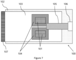
- FIG. 7 shows a plan view of an optical module 100 according to another embodiment.
- the arrangement of Figure 7 is similar to that shown in Figure 1 to 5 , except that the module 100 and housing 102 is configured to house two PICs 101.
- each of the PICs 101 is mounted onto a TCE 104, as described in relation to Figure 5 .
- each of the PICs may be mounted on a chip carrier which is then attached to the TCE, as described in relation to Figure 6 .
- Figure 8 shows a schematic illustration of system comprising an electronic host board 108 and the optical module 100 in accordance with any of the previous embodiments.
- the electronic host board 108 comprises a receptacle 109 into which the module 100 is plugged in.
- the receptacle 109 comprises a receptacle connector 110 that is configured to mate with the electrical plug connector 107 on the module 100 (or alternatively, with the PCB edge connector of Figure 6 (b)).
- the receptacle connector 110 is also referred to as a socket.
- the electronic host board 108 further comprises one or more controllers configured to generate the electronic signals that are then applied into the optical module 100.
- the host board 108 is configured to generate an RF multilevel signal 81 for a coherent source on the module 100; an RF square signal 83 for a gain-switched laser; and an RF square signal 85 for an intensity modulator. These signals may be applied to components on the PIC 101 (via the electrical connection to optical module 100) to generate optical pulses with well-defined properties.
- FIG. 9 shows a schematic illustration of an optical device 900 on the PIC for optical pulse generation.
- the optical device 900 includes phase modulation and intensity modulation.
- the optical device 900 may be referred to as a sending unit.
- the gain switched laser 903 and the coherent light source 901 are integrated on a substrate, as will be described below.
- Phase control element 904 applies a perturbation to the coherent light source 901, such that there is a phase difference between the first half of long light pulse 91 and the second half of long light pulse 91.
- Long light pulse 91 enters light distribution device 902 through port A.
- light distribution device 902 is omitted, and long light pulse 91 travels directly from coherent light source 901 to gain-switched laser 903.
- the phase control element 904 applies a perturbation to the coherent light source 901 at regular intervals, which are timed to occur halfway through the generation of each long light pulse 91.
- the perturbation changes the phase of the second half of the light pulse, producing a phase difference between the first half of a light pulse and the second half of the light pulse.
- the perturbation is controlled, in other words, the same perturbation will always cause the same phase shift.
- the amplitude of the perturbation that is applied affects the phase shift that is generated.
- the perturbation is a short current pulse.
- Alternative embodiments comprise an optical amplifier, for example a semiconductor optical amplifier instead of a gain-switched laser 903.
- Further alternative embodiments comprise an intensity modulator instead of a gain-switched laser 903.
- An intensity modulator modulates the intensity of incoming light pulses. In an “off” state, the intensity modulator reduces the intensity of the light to a low level. In an “on” state, the intensity modulator allows a larger fraction of the incoming light to exit. The intensity modulator is switched between an "on” state and an "off” state twice when the light pulse 91 from the coherent light source is present in order to generate two short light pulses 94.
- the intensity control element 905 provides the switching signal; in this case, the RF signal intensity 85 for the intensity modulator corresponds to the switching signal.
- the phase difference between the two short light pulses is determined by the phase applied to the coherent light pulse 91 by the phase control element 904.
- An intensity modulator may modulate the intensity of the light by changing the absorption coefficient of the material in the modulator, for example an electro-absorption modulator.
- An electro-absorption modulator is a semiconductor device for which the voltage applied to the device changes the absorption coefficient, and therefore the intensity of light travelling through the device.
- the intensity modulator is based on a Mach-Zehnder interferometer. A Mach-Zehnder based intensity modulator changes the phase difference between the two arms of the interferometer to modulate the output intensity.
- Long light pulse 92 exits light distribution device 902 through port B, and is injected into gain-switched laser 903.
- Intensity control element 905 controls the current applied to gain-switched laser 903, in order to modulate the intensity of the double pulses 93 emitted from the gain-switched laser 903.
- the double pulses 93 are emitted from the same aperture through which long light pulse 92 was injected, and enter light distribution device 902 through port B.
- the double pulses exit light distribution device 902 through port C.
- the first pair of light pulses that exit port C of light distribution device 902 have an intensity that has not been modulated by the intensity control element 905, and the phase difference between the pulses is ⁇ 1 .
- the second pair of light pulses that exit port C of the light distribution device 902 have an intensity that has been reduced by intensity control element 905.
- the phase difference between the pulses is ⁇ 2 .
- FIG 10(a) shows a schematic illustration of a gain-switched semiconductor laser.
- a gain-switched laser generates light when the laser is switched above the lasing threshold and generates almost no light when the laser is switched below the lasing threshold.
- Laser 1000 has a controller 1001 which allows modulation of the gain of the laser by modification of the pump power.
- the gain can be modulated in a time varying manner. Driving the laser in this manner can generate short laser pulses (of the order of picoseconds in duration) at the laser output 1002.
- laser 1000 When laser 1000 is a semiconductor laser then it can be pumped electrically, by applying a current. In order to modulate the gain of a semiconductor laser, the controller 1001 modulates the current applied to the laser.
- Figure 10(b) shows three graphs illustrating a gain modulation of a semiconductor gain-switched laser.
- the upper graph shows the current applied to the laser on the vertical axis, with time on the horizontal axis.
- the DC bias is indicated by a horizontal dotted line.
- the current applied to the laser has the form of a series of current modulation pulses.
- the wave is a square-type waveform. In this case, the current is not reduced to zero in between the current modulation pulses, but only reduced to a bias value (which is indicated by the dotted line).
- the current modulation signal is applied to the laser and switches the gain of the laser above and below the lasing threshold periodically.
- the second graph shows the carrier density of the laser on the vertical axis, against time on the horizontal axis.
- the lasing threshold is indicated by a dashed horizontal line.
- the laser output generated by the modulation signal is shown in the lower graph.
- the vertical axis shows the laser intensity, with time on the horizontal axis.
- the laser outputs light when the carrier density is above the lasing threshold. Photons generated by spontaneous emission inside the laser cavity are amplified sufficiently by stimulated emission to generate an output signal.
- the length of the delay between the application of the current modulation pulse and the generation of the output light depends on several parameters, such as the laser type, cavity length and pumping power.
- the rapid increase of the photon density causes a decrease in the carrier density. This in turn decreases the photon density, which increases the carrier density.
- the current modulation pulse is timed to switch back down to the DC bias level, and the laser emission dies off quickly.
- the laser output therefore consists of a train of short laser pulses as shown in the lower graph.
- FIG 10(c) shows a schematic illustration of an electrical driving circuit for a semiconductor gain-switched laser.
- the semiconductor gain-switched laser is laser diode 1005.
- the cathode of laser diode 1005 is connected to bias-T 1006 comprising inductor 1007 and resistor or capacitor 1008.
- bias-T 1006 comprising inductor 1007 and resistor or capacitor 1008.
- Via inductor 1007 a DC bias current is sent through the laser diode. This provides the gain bias (the minimum level of the current indicated by the dotted line in Figure 10(b) ).
- Via resistor or capacitor 1008 an AC modulation current is sent through the laser diode, providing the gain modulation needed for gain-switching the laser above and below the lasing threshold.
- the modulation input to the bias-T 146 is provided by controller 1001.
- the RF multilevel signal 81 for a coherent source on the module 100; the RF square signal 83 for a gain-switched laser; and the RF square signal 85 for an intensity modulator will now be described, with further reference to Figures 9 and 11 .
- Figure 11(b) shows the time varying current 83 applied to gain-switched laser 903 by a controller.
- the signal comprises a square wave, of a magnitude such that the gain-switched laser 903 is switched periodically above the lasing threshold.
- the first current pulse is applied when the first half of light pulse 92 is present.
- the first current pulse is timed such that the gain-switched laser 903 is switched above the lasing threshold during the section of the time when the first half of light pulse 92 is present in the gain-switched laser.
- the second pulse is timed such that the gain-switched laser is switched above the lasing threshold during the section of the time when the second half of the light pulse 92 is present in gain-switched laser 903.
- an RF square signal 87 is read out from a photodetector integrated on the PIC 101 provided in the module 100.
- the RF square signal 87 may correspond to signals read out by a receiver (containing the photodetector) on the PIC 101.
- bases can be selected with different occurrence probabilities.
- a RNG as described below may be used. It is also possible to have jointly an efficient BB84 protocol with decoy states. In this case, multiple output symbols (Zu, Zv, Zw, Xu, Xv, Xw) have to be selected with different probabilities and the RNG described below may be used.
- FIG 12 (a) a QKD setup to implement the standard or the efficient version of the decoy-state BB84 protocol is depicted.
- the embodiment of Figure 12 illustrates a sender, Alice, sending an encrypted key to a receiver, Bob.
- a light source 1286, or photon source, generates a light pulse which is then passed through an intensity modulator 1288.
- the intensity-modulated pulses are then split by an input beam splitter 1290.
- One path - the "first path” - goes through a phase modulator 1292 after the beam splitter 90.
- the phase modulator 1292 randomly modulates the photons by a specific phase, thus outputting the photons with one of (in this embodiment) two bases ⁇ Z, X ⁇ .
- the occurrence ratio between the two bases may be biased or unbiased, and predetermined by a user.
- the efficient version of the BB84 protocol is realized; in the latter case, the standard version of the BB84 protocol is realized.
- the invention disclosed herein can cover both cases, with the unbiased case as a trivial particular case.
- a string processor, or FPGA string processor 1282 is used to control the phase modulator 1292 for the basis selection.
- the FPGA 1282 controlling the basis selection in the phase modulator 1292 of figure 12 is equivalent to the FPGA 1282 that controls the intensity modulator 1288.
- a different string processor or FPGA according to an embodiment may be used to control the phase modulator 1292.
- Light pulses or photons from the first and second path are then sent to the receiver, Bob, via an optical transmission line 1294 and two polarising beam splitters 1296 and 1298.
- Alice's polarising beam splitter 1296 rotates and combines polarised pulses or photons from the two different paths and send them through the optical transmission line 1294.
- Bob's polarising beam splitter 1298 separates them and directs them onto the two paths of his interferometer, this time sending the pulses or photons sent through Alice's phase modulator 1292 through an optical delay 1200 and the pulses or photons not sent through Alice's phase modulator 1292 through phase modulator 1202. This way, the pulses or photons can reach the final beam splitter 1204 at the same time and can interfere.
- Bob's phase modulator 1202 randomly selects one of two bases in which to measure the received pulses or photons, by selecting a phase modulation value. Similar to Alice's phase modulator 1292, Bob's phase modulator 1202 randomly modulates the photons by a specific phase, thus effectively measuring through the detectors 1208 and 1210 the photons with one of (in this embodiment) two bases ⁇ Z, X ⁇ . The occurrence ratio between the two bases is biased, and predetermined by a user to be equal to that of Alice's phase modulator 1292.
- a further string processor or FPGA string processor 1284 may be used to control this second phase modulator 1202 for the basis selection.
- variable delay line 1206 fine tunes the delay in the receiver.
- Photon detectors 1208 and 1210 are then used to measure the result of the interference between the pulses or photons on the two paths; and from these results the key may be derived.
- the key bit value 0 can be assigned if detector 1208 clicks while the key bit value 1 can be assigned if detector 1210 clicks.
- Alice's phase modulator 1292 and Bob's phase modulator 1202 are configured to encode and decode quantum bits respectively.
- At least some of the components of the QKD system of Figure 12 (a) are implemented on the PIC 101 provided in the optical module 100.
- the light source 1286 may be implemented on PIC 101 using the emitter described in Figure 17 below.
- the intensity modulator 1288 may be implemented as a Mach Zehnder Interferometer MZI switch.
- the MZI switch is configured to operate as a variable optical attenuator.
- the MZI switch has two inputs and two outputs. However a single input and/or a single output may be used. At the input side, the inputs are evanescently coupled together and then split into two arms of the interferometer. One arm contains a phase shifter.
- the phase shifter is configured to add a phase to the input light and the amount of phase added may be controlled.
- the phase shifter may be implemented in the same manner as for phase modulator 1292.
- the light passing through the phase shifter interferes with the light that has not passed through the phase shifter and the amplitude of the light at each output of the MZI depends on the relative phase shift.
- the power splitting ratio may be controlled and the power transferred to each output may be controlled.
- the intensity of light output by the intensity modulator 1288 may be controlled.
- the intensity modulator 1288 may be implemented as an electro-absorption modulator (EAM).
- the beam splitter 1290 is implemented as a 2x2 directional coupler; and the delay 1293 is implemented as a delay line, comprising a light guiding section.
- the light guiding section is a few centimetres long.
- the line is approximately 4.5 cm long and provides a delay of approximately 500 ps.
- the different components are optically coupled together by means of light guiding sections integrated on the PIC 101.
- the polarising beam splitter 1296 may be implemented off chip.
- the transmitter 900 of Figure 9 is used as the sending unit.
- This can be driven unit the driving scheme of figure 11 and this removes the need of electro optic modulator. Removing the electro-optic modulators is a way to reduce the power consumption of the chip and it also allows to make the chip more compact. The removal of the electro-optic modulator also simplifies the electronics on the host board.
- the photo detectors 1208 and 1210 is may be implemented on PIC 101 using the receiver described in Figure 16 below.
- Polarising beam splitter 1298, delay 1200, beam splitter 1204 and phase modulator 1202 are implemented in a similar manner as for the sending unit.
- the variable delay line 1206 may be implemented off chip.
- the FPGA 1282 and 1284 are connected to the electronic host board 108 and provide the RF signals for the intensity modulator and the phase modulators. QRNGs provide strings to the string processor (FPGA board) to generate the qubit states.
- FIG 12(b) shows a schematic illustration of a Quantum Key Distribution (QKD) system.
- the QKD system comprises an optical module 100, configured as a transmitter, plugged into a host board (Alice), and another optical module 100, configured as a receiver, plugged into a host board (Bob).
- the module 100 is compatible with different designs and different QKD protocols.
- the same host electric board may drive different quantum transmitters.
- the same transmitter can be used to generate qubits for one or more protocols (BB84, DPS, COW, SARG, RFI, MDI-QKD, TF-QKD).
- the receiver may also be compatible with multiple protocols if for example it is implemented as in GB2564446B .
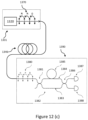
- FIG 12(c) is a schematic illustration of a differential-phase shift quantum communication system (DPS-QKD) in accordance with an example, where the Quantum Transmitter comprises an optical device 1320 with a phase control element such as that shown in Figure 9 .
- DPS-QKD differential-phase shift quantum communication system
- Coherent light source 901 is a semiconductor laser. Coherent light source 901 is configured to generate CW light. In alternative embodiments, the coherent light source generates long light pulses of duration greater than or equal to 10ns.
- phase control element 904 may apply a short current pulse to coherent light source 901. This results in a phase difference between a first part and a second part of the CW light.
- the CW light enters gain-switched laser 903, which generates a first short pulse when the first part of the light is incident, and generates a second short pulse when the second part of the light is incident. There is a phase difference between the generated short light pulses equal to the phase difference between the first part and second part.
- the phase control element 904 encodes information between consecutive pulses by controlling the phase difference between parts of the generated CW light. In this DPS-QKD example, the intensity control element 905 of Figure 9 is not used.
- phase control element 904 is configured to introduce a phase shift of either 0 or ⁇ between subsequent pulses to generate the sequence of light pulses 1370.
- phase control element 904 applies no short current pulse to coherent light source 901 initially, resulting in no phase difference between the first part and the second part of the CW light, and thus no phase difference between the first and second short light pulses.
- phase control element 904 then applies a short current pulse to coherent light source 901, resulting in a phase difference of ⁇ between the second part and the third part of the CW light, and thus a phase difference of ⁇ between pulse 2 and 3.
- phase control element 904 applies a short current pulse of a particular amplitude to coherent light source 901, resulting in a phase difference of ⁇ between the third and fourth part of the CW light, and thus a phase difference of ⁇ between pulses 3 and 4 in the sequence.
- a phase difference of 0 between subsequent pulses is associated with a bit value of 0.
- a phase difference of ⁇ between subsequent pulses is associated with a bit value of 1.
- the phase control element 904 may set the differential phase between subsequent light pulses.
- a phase difference of 0 between subsequent pulses may be associated with a bit value of 0, while a phase difference of ⁇ between subsequent pulses may be associated with a bit value of 1.
- the light pulses are transmitted to a quantum receiver (Bob) which detects the phase difference between the coherent pulses received and decodes a bit value of 0 or 1.
- Bob quantum receiver
- the coherent light source 901 is turned off periodically to randomise the phase after each qubit emission cycle which is required by some quantum communication protocols, for example, the BB84 protocol.
- Some quantum communication protocols for example, the BB84 protocol.
- An example operation is shown in Figure 11(a) .
- the coherent light source 901 emits long coherent light pulses.
- the gain switched laser 903 is driven with two subsequent pulses during the time that a long coherent pulse is emitted by light source 901, generating a time-bin encoded qubit.
- the relative phase ⁇ 1 of the two time-bins encode a desired qubit state, for example, according to the DPS-QKD protocol described above.
- the system described herein can be configured as required for the different protocols. For example, 2 phase states are used in the DPS protocol, and 4 phase states for the BB84 protocol. For the DPS protocol phase randomisation is not needed. For decoy states protocols the further intensity modulator is needed.
- the encoded qubits are then sent to Bob.
- the quantum receiver 1390 comprises an asymmetric MZI 1382 with an optical delay 1385 which is equal to the time delay ⁇ t between two subsequent pulses of coherent pulse sequence 1370.
- the delay line is optional.
- a transmitter 900 of the type shown in figure 9 there is no delay line in the transmitter 900 and hence the delay between the two pulses can be freely adjusted to match the delay of the receiver. Therefore a variable delay line is not needed in the receiver when using a transmitter 900.
- the pulse sequence 1380 enters one input of beam splitter 1381.
- a first output of input beam splitter 1381 is connected to the long arm 1384 of the interferometer 1382, and a second output is connected to the short arm 1383 of the interferometer 1382.
- a first fraction of each pulse of the pulse sequence 1380 is sent along the short arm 1383 of interferometer 1382 and a second fraction is sent along the long arm 1384 of interferometer 1382.
- the long arm 1384 is connected to a first input of output beam splitter 1386 and the short arm is connected to a second input of output beam splitter 1386.
- subsequent pulses of pulse sequence 1380 are overlapped in time. For example, a second fraction of the first light pulse (which has travelled the long arm 1384) will arrive at the output beam splitter 1386 at the same time as a first fraction of the second light pulse (which has travelled the short arm 1383).
- the pulses are coherent and therefore they interfere at the beam splitter.
- the output depends on the phase difference. If the phase difference is zero there is a detection at detector 1387. If, on the other hand, the phase difference is ⁇ , there is a detection at detector 1388. For any other value of difference between the phase modulation applied at the phase modulator, there will be a finite probability that a photon may output at detector 1387 or detector 1388.
- the phase difference between the second fraction of the first light pulse and the first fraction of the second light pulse is zero, therefore detector 1387 registers a detection. This corresponds to a bit value of 0.
- the phase difference between the second fraction of the second light pulse and the first fraction of the third light pulse is ⁇ , therefore the detector 1388 registers a detection.
- Both the fractions of each light pulse interfere and can give rise to a detection.
- the second fraction of the nth pulse can always interfere with the first fraction of the (n+1)th pulse and result in a detection. This happens because each pulse is coherent with the following one.
- Which detector registers a detection depends on whether the phase value is 0 or ⁇ .
- the temperature of the PIC is also stabilised to maximize the interference visibility.
- each photon will either go along the long arm or the short arm. In these cases, a photon detected at any detector cannot lead to a detection event in any other detector.
- an attenuator reduces the intensity of the light pulses emitted from the optical device.
- the intensity is reduced such that the light pulses comprise 10 or fewer photons.
- the average number of photons per pulse is less than 1.
- the PIC 101 is configured as other quantum devices.
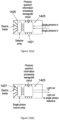
- Figures 13(a) to (c) and Figures 14(a) to (c) show examples of the PIC 101 configured as a quantum random number generator (QRNG)
- FIG. 13(a) shows a PIC 1401 that comprises: a gain-switched laser 1403; a time delay interferometer 1405, which is also referred to as an asymmetric Mach Zehnder interferometer (AMZI), and a photodetector 1405.
- the gain-switched laser 1403 is configured to produce pulses that each have a random phase in relation to one another, as described herein.
- the pulses are directed to the AMZI 1405 via light guiding sections (not shown).
- the AMZI is similar to the MZI described above except that the long arm comprises a delay element.
- the delayed and non-delayed pulses are caused to interfere in a 2x2 directional coupler in the AMZI and the interfered pulses are directed to the photodetector 1407 where the intensities of the interfered pulses are converted to a signal.
- the signal corresponding to the intensities of the interfered pulses has a random value because the phases of the reference and delayed pulses are random. Random numbers may be generated from the random intensities of the interfered pulses.
- the photodetector may be on chip (integrated in the PIC 101) as shown in figure 13(a) and 13(b) or off chip as shown in figure 13(c) .
- the optical interface 105, 106 of the module 100 is used to couple light from the PCI 101 to the photodetector provided off the chip. If on chip, the electrical interface of the module is used to read out the measured intensities.
- the gain switched laser may be on chip (integrated in the PIC 101) as shown in figure 13(a) and 13(c) or off chip as shown in figure 13(b) . If off chip, the optical interface 105, 106 of the module 100 is used to couple light from the gain switched laser provided off the chip to the PIC.
- Figures 14(a) to 14(c) show further examples of PICs 1411. However, here instead of the AMZI of figures 13(a) to 13(c) , a multimode interferometer is used.
- two independent pulsed lasers laser 1 1412 and laser 2 1413, are driven at equal repetition rates.
- the two lasers 1412, 1413 output light at the same intensity and wavelengths.
- each pulse from the stream of pulses may have a random phase.
- the streams of pulses from each laser are independent from each other and therefore the pulses from each laser have random phases relative to each other.
- the pulses from the two lasers temporally overlap and are interfered in multimode interferometer 1415, which may be, for example, a 2x2 directional coupler or a beam splitter.
- the interfered signal is sent to a photodetector 1417 where the intensity of the interfered pulse is converted to a signal.
- the signal corresponding to the intensity of the interfered pulse has a random value because the phases of the pulses from laser 1 1412 and laser 2 1413 are random. Random numbers may be generated from the random intensity of the interfered pulses.
- the photodetector 1417 may be on chip (integrated in the PIC 101) as shown in figures 14(a) and 14(b) or off chip as shown in figure 14(c) . If off chip, the optical interface 105, 106 of the module 100 is used to couple light from the PCI 101 to the photodetector provided off the chip. If on chip, the electrical interface of the module is used to read out the measured intensities.
- the gain switched lasers 1412 and 1413 may be on chip (integrated in the PIC 101) as shown in figure 14(a) and 14(c) or off chip as shown in figure 14(b) . If off chip, the optical interface 105, 106 of the module 100 is used to couple light from the gain switched lasers provided off the chip to the PIC 101.
- the light it is also possible for the light to be processed to be generated off the chip and for the light signals output from the processor to be detected off the chip.
- Figure 15(c) Such an arrangement is shown in Figure 15(c) .
- the light enters the chip and the light exits the chip from the same side.
- Figure 16 shows an example of a fabrication sequence for a device that may be used in the receiver.
- the receiver is the type of device described for example in GB2551483 . For completeness a description of this device is included below.
- the device is an avalanche photodiode which is part of a photon detection device.
- the device comprises detection regions with an avalanche multiplication region integrated on a semiconductor substrate.
- the device may be fabricated from one or more semiconductor materials, depending on the wavelength of the light which it is designed to detect.
- Each detection region comprises an avalanche multiplication region.
- For each detection region there is a corresponding contact.
- the contact is an anode contact, however it will be appreciated that this could alternatively be a cathode contact.
- Each anode contact is connected to a metal contact region 308.
- the basis for the heterostructure is a substrate 301, on which the subsequent layer structure is fabricated.
- the substrate may be an InP substrate for example.
- the second layer 302 is deposited on said substrate 301.
- the second layer 302 may be an un-doped or lightly doped n-type InGaAs layer for example.
- This layer may be a highly doped n-type InP layer for example.
- a cross-sectional view of the device at this stage in fabrication is shown in i.
- guard ring regions 306 are also incorporated into the first layer 303.
- the guard ring regions may be formed in the same step as the highly doped regions 305, or in a separate step, and by the same method or by a different method.
- a cross-sectional view of the device at this stage in fabrication is shown in ii.
- the first 303 and second 302 layers may be silicon, in which p-type and n-type doping may be achieved using Boron or Phosphorous impurities respectively.
- the device may alternatively be based on a Silicon - Germanium heterostructure or based on any of the Ill-V class of semiconductors.
- the device comprises highly n-doped regions 305 which are incorporated into a moderately doped n-type heterolayer 303, for example by gas immersion laser doping, implantation or diffusion.
- the passivation layer 307 is deposited on the surface of the device, except for a portion of the surface above each highly doped region 305.
- the passivation layer 307 may be a dielectric, for example silicon nitride or silicon oxide.
- a cross-sectional view of the device at this stage in fabrication is shown in iii.
- the metal contact region 308 corresponding to each detection region is then deposited on the edge portion of the passivation layer and the outer portion of the inner portion of the highly doped region 305.
- the metal contact region 308 may be a Chromium/Gold double layer where the highly doped p-type regions are InP.
- the metal contact region on the opposite surface of the substrate to the fabricated layers may be a different metal or semiconductor.
- An anti-reflective coating 309 may be deposited on the remaining portion of the highly doped regions 305.
- the material of the anti-reflective coating 309 may depend on the wavelength of light intended for the detector. For example, for an InP based detector, silicon nitride with a selected thickness may be used so that the reflection at the surface is minimal.
- two detectors are fabricated as there are two exposed portions of highly doped regions 305.
- the fabrication can also be used for just one detector.
- FIG 17(a) and 17(b) show a schematic illustration of a distributed Bragg reflector (DBR) laser that can be provided on the PIC 101 in order to implement the coherent source 901 or the gain-switched laser 903.
- DBR distributed Bragg reflector
- Figure 17(a) and (b) show a DBR laser, it will be understood that a distributed feedback (DFB) lasers or ridge lasers may alternatively be used.
- DBR distributed Bragg reflector
- the lasers may comprise a grating region.
- the grating region may be separate from the active region or the active region may comprise the grating.
- a laser where the active region and grating are separate is referred to as DBR (distributed Bragg reflector) laser.
- DBR distributed Bragg reflector
- a DBR is shown in Figure 17(a) and Figure 17(b) .
- a laser where the active region comprises the grating is a DFB laser.
- a DBR is shown in Figure 17(a) and 17(b).
- Figure 17(a) shows a side view of the DBR
- Figure 17(b) shows a cross-section front view.
- the active area comprises a multi quantum well region (MQW).
- the MQW region comprises a plurality of quantum well layers.
- the MQW region comprises alternating layers of materials such as, for example: AlInGaAs/InP, AlInGaAs/AlInAs, InGaAsP/InP, InGaAsP/AllnAs or InGaAs/AlInGaAs. All these layers are lattice matched to an InP substrate.
- the device comprises a substrate 400. On one surface of the substrate is an n-contact 426. Overlying and in contact with the opposite surface to the substrate 400 is the buffer layer 406. Both the substrate 400 and the buffer layer 406 are n-type layers. Alternatively, the structure can be reversed, such that the substrate 400 is a p-type layer. The layers may be n-doped InP. Overlying and in contact with the buffer layer 406 is the n-type layer 408. The n-type layer 408 may be n-doped InP. Overlying and in contact with a strip of the n-type layer 408 is a first waveguide material 410a. Overlying and in contact with the first waveguide material 410a is a MQW layer 412.
- a second waveguide material 410b Overlying and in contact with the MQW layer 410 is a second waveguide material 410b.
- a p-type material 416 On either side of the strip and overlying and in contact with the n-type material 408 is a p-type material 416, which may be p-doped InP.
- An n-type layer 418 is overlying and in contact with the p-type layer 416, and may be n-doped InP.
- the p-type layer 420 is overlying and in contact with the second waveguide layer 410b and the n-type layer 418, and may be p-doped InP.
- a p-type contact layer 422 is overlying and in contact with the p-type layer 420.
- the p-type contact layer 422 is heavily doped InP, i.e. having a dopant concentration higher than that of layer 420.
- a p-contact metal 424 is overlying and in contact with part of the p-contact layer 422.
- the MQW strip runs along the length of the device.
- a current is applied between the first p-contact 424 and the n-contact 426 in order to generate light in the MQW strip of the coherent light source 20.
- Light generated in the MQW strip of the laser is emitted along the MQW layer.
- the light is laterally confined by the p-type layer 416 and vertically confined by the waveguide layers 410a and b.
- the light exits the MQW layer through an aperture of the laser.
Landscapes
- Physics & Mathematics (AREA)
- Engineering & Computer Science (AREA)
- Optics & Photonics (AREA)
- General Physics & Mathematics (AREA)
- Nanotechnology (AREA)
- Chemical & Material Sciences (AREA)
- Computer Networks & Wireless Communication (AREA)
- Signal Processing (AREA)
- Electromagnetism (AREA)
- Microelectronics & Electronic Packaging (AREA)
- Crystallography & Structural Chemistry (AREA)
- Life Sciences & Earth Sciences (AREA)
- Biophysics (AREA)
- Mathematical Physics (AREA)
- Theoretical Computer Science (AREA)
- Semiconductor Lasers (AREA)
- Optical Communication System (AREA)
- Optical Couplings Of Light Guides (AREA)
- Optical Modulation, Optical Deflection, Nonlinear Optics, Optical Demodulation, Optical Logic Elements (AREA)
Claims (11)
- Système comprenant :un module optique (100) ; etune carte électronique hôte (108) ;dans lequel le module optique (100) est configuré pour être branché dans la carte électronique hôte (108), le module optique comprenant :un circuit intégré photonique quantique (101) ;un élément de commande de température, TCE (104) ;un boîtier (102) configuré pour abriter ledit circuit intégré photonique quantique (101) et ledit élément de commande de température (104) ; etune carte de circuit imprimé (103) configurée pour acheminer des signaux électriques vers et/ou depuis le circuit intégré photonique quantique (101),dans lequel le circuit intégré photonique quantique (101) est fixé à l'élément de commande de température (104), de telle sorte que ledit circuit intégré photonique quantique (101) est en communication thermique avec ledit élément de commande de température (104) ; etl'élément de commande de température (104) est fixé directement au boîtier (102), dans lequel l'élément de commande de température (104) est fixé au boîtier (102) sans aucune autre pièce entre ceux-ci ou l'élément de commande de température (104) est fixé au boîtier (102) avec un matériau d'interface thermique entre ceux-ci, de telle sorte que ledit élément de commande de température (104) est en communication thermique directe avec le boîtier (102) de telle sorte que le boîtier est configuré pour dissiper de la chaleur générée par l'élément de commande de température,la carte électronique hôte (108) comprend une fiche (110), et, dans lequel la carte de circuit imprimé (103) comprend un connecteur (107) configuré pour se brancher dans la fiche (110),le boîtier comprenant en outre un réceptacle d'élément de commande de température (102b) qui est configuré pour recevoir le TCE (104), le réceptacle de TCE (102b) étant configuré pour ajuster la hauteur du circuit intégré photonique quantique (101) par rapport à la carte de circuit imprimé (103).
- Système selon la revendication 1, dans lequel le module (100) comprend une puce d'interposition (103b), dans lequel le circuit intégré photonique quantique (101) est fixé à la puce d'interposition (103b), et la puce d'interposition (103b) est fixée à l'élément de commande de température (104), de telle sorte que le circuit intégré photonique quantique (101) est en communication thermique avec ledit élément de commande de température (104).
- Système selon la revendication 2, dans lequel la puce d'interposition (103b) comprend un support de puce thermiquement conducteur.
- Système selon l'une ou l'autre de la revendication 2 ou de la revendication 3, dans lequel la puce d'interposition (103b) est configurée pour acheminer des signaux électriques du circuit intégré photonique quantique (101) à la carte de circuit imprimé (103).
- Système selon une quelconque revendication précédente, dans lequel le circuit intégré photonique quantique (101) est configuré pour fonctionner en tant qu'au moins l'un parmi :un émetteur de communication quantique;un récepteur de communication quantique ;un générateur de nombres aléatoires quantique ; etun processeur informatique quantique.
- Système selon une quelconque revendication précédente, dans lequel la carte électronique hôte (108) est configurée pour générer un signal électrique destiné à commander le circuit intégré photonique quantique (101).
- Système selon une quelconque revendication précédente, dans lequel la carte électronique hôte (108) est configurée pour générer un signal électrique destiné à commander l'élément de commande de température (104).
- Système selon une quelconque revendication précédente, dans lequel la carte électronique hôte (108) est configurée pour acquérir un signal électrique généré par le circuit intégré photonique quantique (101).
- Unité d'envoi destinée à un système de communication quantique, l'unité d'envoi comprenant :
le système selon une quelconque revendication précédente, dans laquelle le circuit intégré photonique quantique (101) est configuré pour fonctionner en tant qu'émetteur de communication quantique, et le circuit intégré photonique quantique (101) comprend :une source de bits quantiques configurée pour générer des bits quantiques ;un codeur de bits quantiques configuré pour coder les bits quantiques générés destinés à l'envoi à une unité de réception ; etun élément de commande d'intensité configuré pour moduler l'intensité des bits quantiques. - Unité de réception destinée à un système de communication quantique, l'unité de réception comprenant :
le système selon une quelconque revendication précédente, lorsqu'elle dépend de la revendication 6, dans lequel le circuit intégré photonique quantique (101) est configuré pour fonctionner en tant que récepteur de communication quantique, et le circuit intégré photonique quantique (101) comprend un décodeur de bits quantiques configuré pour décoder des bits quantiques codés générés par une unité d'envoi. - Système de communication quantique comprenant :l'unité d'envoi selon la revendication 9 ;l'unité de réception selon la revendication 10 ; etune liaison optique configurée pour connecter l'unité d'envoi à l'unité de réception.
Applications Claiming Priority (1)
| Application Number | Priority Date | Filing Date | Title |
|---|---|---|---|
| GB2018329.9A GB2601172B (en) | 2020-11-20 | 2020-11-20 | An optical module, a system, a sending unit, a receiving unit, and a quantum communication system |
Publications (2)
| Publication Number | Publication Date |
|---|---|
| EP4001981A1 EP4001981A1 (fr) | 2022-05-25 |
| EP4001981B1 true EP4001981B1 (fr) | 2025-04-30 |
Family
ID=74046966
Family Applications (1)
| Application Number | Title | Priority Date | Filing Date |
|---|---|---|---|
| EP21188871.4A Active EP4001981B1 (fr) | 2020-11-20 | 2021-07-30 | Module optique, système, unité d'émission, unité de réception, et système de communication quantique |
Country Status (4)
| Country | Link |
|---|---|
| US (1) | US11509399B2 (fr) |
| EP (1) | EP4001981B1 (fr) |
| JP (1) | JP7214773B2 (fr) |
| GB (1) | GB2601172B (fr) |
Families Citing this family (18)
| Publication number | Priority date | Publication date | Assignee | Title |
|---|---|---|---|---|
| US12029004B2 (en) | 2020-09-18 | 2024-07-02 | Nubis Communications, Inc. | Data processing systems including optical communication modules |
| EP4226195A4 (fr) | 2020-10-07 | 2024-10-02 | Nubis Communications, Inc. | Systèmes de traitement de données comprenant des modules de communication optique |
| TW202238198A (zh) | 2020-11-20 | 2022-10-01 | 美商紐比斯通訊股份有限公司 | 用於具有光通訊模組之機架安裝系統的熱設計 |
| US12066653B2 (en) | 2021-04-22 | 2024-08-20 | Nubis Communications, Inc. | Communication systems having optical power supplies |
| US12495487B2 (en) * | 2021-06-11 | 2025-12-09 | Intel Corporation | Flex-PCB integrated packaging for silicon photonics LiDAR |
| US12461322B2 (en) | 2021-06-17 | 2025-11-04 | Nubis Communications, Inc. | Communication systems having pluggable modules |
| WO2022266376A1 (fr) | 2021-06-17 | 2022-12-22 | Nubis Communications, Inc. | Systèmes de communication comprenant des modules enfichables |
| EP4152065A1 (fr) | 2021-09-16 | 2023-03-22 | Nubis Communications, Inc. | Systèmes de communication ayant des modules optiques co-emballés |
| US12250024B2 (en) | 2021-09-16 | 2025-03-11 | Nubis Communications, Inc. | Data processing systems including optical communication modules |
| US20230352465A1 (en) * | 2022-04-28 | 2023-11-02 | Lightmatter, Inc. | Led-based photonic communication and processing unit |
| WO2023215315A1 (fr) | 2022-05-02 | 2023-11-09 | Nubis Communications, Inc. | Systèmes de communication ayant des modules optiques enfichables |
| GB2623747A (en) * | 2022-10-19 | 2024-05-01 | Toshiba Kk | A photonic integrated circuit |
| US12546937B2 (en) * | 2022-11-17 | 2026-02-10 | Panduit Corp. | Photonic fabric chip device |
| GB2625806A (en) * | 2022-12-23 | 2024-07-03 | Light Trace Photonics Ltd | Housing for accommodating a photonic integrated circuit chip |
| CN116184584B (zh) * | 2023-02-21 | 2023-11-03 | 讯芸电子科技(中山)有限公司 | 一种内埋tec基板的400g硅光集成光模块 |
| DE102023131121A1 (de) * | 2023-11-09 | 2025-05-15 | XCCES GmbH | Optisches System und Verfahren zur Herstellung und Betrieb |
| GB2639859A (en) * | 2024-03-25 | 2025-10-08 | Toshiba Kk | Optical quantum random number generators |
| US20250314718A1 (en) * | 2024-04-04 | 2025-10-09 | Ii-Vi Delaware, Inc. | Pcsel magnetometer |
Family Cites Families (27)
| Publication number | Priority date | Publication date | Assignee | Title |
|---|---|---|---|---|
| JPH10247741A (ja) * | 1997-03-04 | 1998-09-14 | Nippon Telegr & Teleph Corp <Ntt> | 光通信用発光モジュールおよびその組立方法 |
| US6155724A (en) * | 1997-03-04 | 2000-12-05 | Hamamatsu Photonics Kk | Light transmitting module for optical communication and light transmitting unit thereof |
| US7149430B2 (en) * | 2001-02-05 | 2006-12-12 | Finsiar Corporation | Optoelectronic transceiver having dual access to onboard diagnostics |
| US6762938B2 (en) * | 2001-03-16 | 2004-07-13 | Coretek, Inc. | Apparatus and method for providing auxiliary cooling and thermal stability to an opto-electronic component |
| JP3909257B2 (ja) * | 2002-03-12 | 2007-04-25 | 日本オプネクスト株式会社 | 光結合装置 |
| JP2005099166A (ja) * | 2003-09-22 | 2005-04-14 | Toshiba Corp | 光送信モジュールおよび光送信装置 |
| US8079222B2 (en) * | 2008-01-31 | 2011-12-20 | Applied Optoelectronics, Inc. | Thermoelectric cooler controller |
| GB0917060D0 (en) * | 2009-09-29 | 2009-11-11 | Qinetiq Ltd | Methods and apparatus for use in quantum key distribution |
| JP5471813B2 (ja) * | 2010-05-18 | 2014-04-16 | 住友電気工業株式会社 | 光トランシーバ |
| US8929748B2 (en) * | 2010-03-16 | 2015-01-06 | Source Photonics | Tunable dense wavelength division multiplexing transceiver, circuits and devices therefor, and methods for making and using such transceivers, circuits and devices |
| US20110299858A1 (en) * | 2010-06-08 | 2011-12-08 | Cisco Technology, Inc. | Host device with multipurpose optics drive capabilities |
| KR101430634B1 (ko) * | 2010-11-19 | 2014-08-18 | 한국전자통신연구원 | 광 모듈 |
| US8750710B1 (en) * | 2011-07-15 | 2014-06-10 | Cisco Technology, Inc. | System and method for facilitating fiber access transport using pluggable radio frequency optics |
| US8905632B2 (en) * | 2011-11-29 | 2014-12-09 | Cisco Technology, Inc. | Interposer configuration with thermally isolated regions for temperature-sensitive opto-electronic components |
| US8812760B1 (en) * | 2011-12-22 | 2014-08-19 | Cisco Technology, Inc. | System and method for monitoring two-wire communication in a network environment |
| JP5948695B2 (ja) * | 2012-02-28 | 2016-07-06 | 住友電工デバイス・イノベーション株式会社 | 光モジュール、光モジュール生産物 |
| CN105684170B (zh) * | 2013-08-09 | 2019-09-03 | 株式会社光波 | 发光装置 |
| GB2537821B (en) | 2015-04-21 | 2017-04-19 | Toshiba Res Europe Ltd | An optical device |
| GB2551483B (en) | 2016-06-13 | 2020-05-27 | Toshiba Res Europe Limited | A photon detection device and a method of manufacturing a photon detection device |
| US10012809B2 (en) | 2016-06-20 | 2018-07-03 | Mellanox Technologies, Ltd. | Printed circuit board assembly with a photonic integrated circuit for an electro-optical interface |
| GB2555398B (en) | 2016-10-24 | 2020-04-08 | Toshiba Kk | An optoelectronic system and method for its fabrication |
| GB2564446B (en) | 2017-07-10 | 2020-01-22 | Toshiba Kk | A Quantum communication component, receiver and system |
| US10725254B2 (en) * | 2017-09-20 | 2020-07-28 | Aayuna Inc. | High density opto-electronic interconnection configuration utilizing passive alignment |
| CN116661072A (zh) * | 2017-09-24 | 2023-08-29 | 申泰公司 | 有通用定位的光收发器 |
| US20190391348A1 (en) * | 2018-02-19 | 2019-12-26 | Infinera Corporation | Heterogeneous common substrate multi-chip package including photonic integrated circuit and digital signal processor |
| CN110177447A (zh) * | 2019-06-25 | 2019-08-27 | 中磊电子(苏州)有限公司 | 散热机壳、其制造方法及应用其的电子装置 |
| KR102175952B1 (ko) * | 2019-06-28 | 2020-11-09 | 한국전자통신연구원 | 양자통신 제어장치, 그것을 포함하는 양자통신 시스템 및 그것의 설계 방법 |
-
2020
- 2020-11-20 GB GB2018329.9A patent/GB2601172B/en active Active
-
2021
- 2021-02-26 US US17/187,484 patent/US11509399B2/en active Active
- 2021-03-16 JP JP2021042270A patent/JP7214773B2/ja active Active
- 2021-07-30 EP EP21188871.4A patent/EP4001981B1/fr active Active
Also Published As
| Publication number | Publication date |
|---|---|
| GB2601172A (en) | 2022-05-25 |
| GB202018329D0 (en) | 2021-01-06 |
| US11509399B2 (en) | 2022-11-22 |
| US20220166522A1 (en) | 2022-05-26 |
| JP7214773B2 (ja) | 2023-01-30 |
| GB2601172B (en) | 2025-02-05 |
| EP4001981A1 (fr) | 2022-05-25 |
| JP2022082406A (ja) | 2022-06-01 |
Similar Documents
| Publication | Publication Date | Title |
|---|---|---|
| US11509399B2 (en) | Optical module, a system, a sending unit, a receiving unit, and a quantum communication system | |
| US11709657B2 (en) | High bandwidth quantum random number generator | |
| US11749968B2 (en) | Dual grating-coupled lasers | |
| Mahgerefteh et al. | Techno-economic comparison of silicon photonics and multimode VCSELs | |
| Denoyer et al. | Hybrid silicon photonic circuits and transceiver for 50 Gb/s NRZ transmission over single-mode fiber | |
| US8078063B2 (en) | Monolithic power monitor and wavelength detector | |
| Wang et al. | Silicon photonic transceivers for application in data centers | |
| US10027089B2 (en) | Coupled ring resonator system | |
| US8089995B2 (en) | Structures and methods for adjusting the wavelengths of lasers via temperature control | |
| Trenti et al. | On-chip quantum communication devices | |
| Kanazawa et al. | 30-km error-free transmission of directly modulated DFB laser array transmitter optical sub-assembly for 100-Gb application | |
| Kim et al. | Single-chip photonic transceiver based on bulk-silicon, as a chip-level photonic I/O platform for optical interconnects | |
| Yao et al. | Monolithic 300 Gb/s parallel transmitter in InP-based generic photonic integration technology | |
| Ohyama et al. | Compact hybrid integrated 100-Gb/s transmitter optical sub-assembly using optical butt-coupling between EADFB lasers and silica-based AWG multiplexer | |
| Abbasi et al. | 43 Gb/s NRZ-OOK direct modulation of a heterogeneously integrated InP/Si DFB laser | |
| US20220043634A1 (en) | Compact Digitization System for Generating Random Numbers | |
| Turkiewicz et al. | High speed optical data transmission with compact 850 nm TO-can assemblies | |
| Kanazawa et al. | 224-Gbit/s 4-PAM operation of compact DC block circuit integrated hi-FIT AXEL transmitter with low power consumption | |
| Yun et al. | Compact hybrid-integrated 4× 80-Gbps TROSA module using optical butt-coupling of DML/SI-PD and silica AWG chips | |
| US8891971B1 (en) | Signal quality in bi-directional optical links using optical circulators | |
| Yun et al. | Optical subassembly modules using light sources butt-coupled with silica-based PLC | |
| Aruga et al. | Recent progress with next generation high-speed Ethernet optical device technology | |
| EP4576611A1 (fr) | Dispositifs optiques, émetteur optique et générateur de nombres aléatoires quantiques optiques | |
| Bassinan et al. | Toward future generation digital avionics fiber optic communication | |
| Urino et al. | Photonics-electronics convergence system for high density inter-chip interconnects by using silicon photonics |
Legal Events
| Date | Code | Title | Description |
|---|---|---|---|
| PUAI | Public reference made under article 153(3) epc to a published international application that has entered the european phase |
Free format text: ORIGINAL CODE: 0009012 |
|
| STAA | Information on the status of an ep patent application or granted ep patent |
Free format text: STATUS: REQUEST FOR EXAMINATION WAS MADE |
|
| 17P | Request for examination filed |
Effective date: 20210730 |
|
| AK | Designated contracting states |
Kind code of ref document: A1 Designated state(s): AL AT BE BG CH CY CZ DE DK EE ES FI FR GB GR HR HU IE IS IT LI LT LU LV MC MK MT NL NO PL PT RO RS SE SI SK SM TR |
|
| STAA | Information on the status of an ep patent application or granted ep patent |
Free format text: STATUS: EXAMINATION IS IN PROGRESS |
|
| 17Q | First examination report despatched |
Effective date: 20230616 |
|
| GRAP | Despatch of communication of intention to grant a patent |
Free format text: ORIGINAL CODE: EPIDOSNIGR1 |
|
| STAA | Information on the status of an ep patent application or granted ep patent |
Free format text: STATUS: GRANT OF PATENT IS INTENDED |
|
| RIC1 | Information provided on ipc code assigned before grant |
Ipc: B82Y 20/00 20110101ALN20241004BHEP Ipc: B82Y 10/00 20110101ALN20241004BHEP Ipc: G02B 6/42 20060101AFI20241004BHEP |
|
| INTG | Intention to grant announced |
Effective date: 20241029 |
|
| RIC1 | Information provided on ipc code assigned before grant |
Ipc: B82Y 20/00 20110101ALN20241022BHEP Ipc: B82Y 10/00 20110101ALN20241022BHEP Ipc: G02B 6/42 20060101AFI20241022BHEP |
|
| GRAS | Grant fee paid |
Free format text: ORIGINAL CODE: EPIDOSNIGR3 |
|
| GRAA | (expected) grant |
Free format text: ORIGINAL CODE: 0009210 |
|
| STAA | Information on the status of an ep patent application or granted ep patent |
Free format text: STATUS: THE PATENT HAS BEEN GRANTED |
|
| RBV | Designated contracting states (corrected) |
Designated state(s): AL AT BE BG CH CY CZ DE DK EE ES FI FR GR HR HU IE IS IT LI LT LU LV MC MK MT NL NO PL PT RO RS SE SI SK SM TR |
|
| AK | Designated contracting states |
Kind code of ref document: B1 Designated state(s): AL AT BE BG CH CY CZ DE DK EE ES FI FR GR HR HU IE IS IT LI LT LU LV MC MK MT NL NO PL PT RO RS SE SI SK SM TR |
|
| REG | Reference to a national code |
Ref country code: CH Ref legal event code: EP |
|
| REG | Reference to a national code |
Ref country code: IE Ref legal event code: FG4D |
|
| REG | Reference to a national code |
Ref country code: DE Ref legal event code: R096 Ref document number: 602021029897 Country of ref document: DE |
|
| PGFP | Annual fee paid to national office [announced via postgrant information from national office to epo] |
Ref country code: FR Payment date: 20250610 Year of fee payment: 5 |
|
| REG | Reference to a national code |
Ref country code: NL Ref legal event code: MP Effective date: 20250430 |
|
| REG | Reference to a national code |
Ref country code: AT Ref legal event code: MK05 Ref document number: 1790525 Country of ref document: AT Kind code of ref document: T Effective date: 20250430 |
|
| PG25 | Lapsed in a contracting state [announced via postgrant information from national office to epo] |
Ref country code: ES Free format text: LAPSE BECAUSE OF FAILURE TO SUBMIT A TRANSLATION OF THE DESCRIPTION OR TO PAY THE FEE WITHIN THE PRESCRIBED TIME-LIMIT Effective date: 20250430 Ref country code: PT Free format text: LAPSE BECAUSE OF FAILURE TO SUBMIT A TRANSLATION OF THE DESCRIPTION OR TO PAY THE FEE WITHIN THE PRESCRIBED TIME-LIMIT Effective date: 20250901 Ref country code: FI Free format text: LAPSE BECAUSE OF FAILURE TO SUBMIT A TRANSLATION OF THE DESCRIPTION OR TO PAY THE FEE WITHIN THE PRESCRIBED TIME-LIMIT Effective date: 20250430 |
|
| PGFP | Annual fee paid to national office [announced via postgrant information from national office to epo] |
Ref country code: DE Payment date: 20250604 Year of fee payment: 5 |
|
| REG | Reference to a national code |
Ref country code: LT Ref legal event code: MG9D |
|
| PG25 | Lapsed in a contracting state [announced via postgrant information from national office to epo] |
Ref country code: NO Free format text: LAPSE BECAUSE OF FAILURE TO SUBMIT A TRANSLATION OF THE DESCRIPTION OR TO PAY THE FEE WITHIN THE PRESCRIBED TIME-LIMIT Effective date: 20250730 Ref country code: GR Free format text: LAPSE BECAUSE OF FAILURE TO SUBMIT A TRANSLATION OF THE DESCRIPTION OR TO PAY THE FEE WITHIN THE PRESCRIBED TIME-LIMIT Effective date: 20250731 |
|
| PG25 | Lapsed in a contracting state [announced via postgrant information from national office to epo] |
Ref country code: NL Free format text: LAPSE BECAUSE OF FAILURE TO SUBMIT A TRANSLATION OF THE DESCRIPTION OR TO PAY THE FEE WITHIN THE PRESCRIBED TIME-LIMIT Effective date: 20250430 Ref country code: PL Free format text: LAPSE BECAUSE OF FAILURE TO SUBMIT A TRANSLATION OF THE DESCRIPTION OR TO PAY THE FEE WITHIN THE PRESCRIBED TIME-LIMIT Effective date: 20250430 |
|
| PG25 | Lapsed in a contracting state [announced via postgrant information from national office to epo] |
Ref country code: BG Free format text: LAPSE BECAUSE OF FAILURE TO SUBMIT A TRANSLATION OF THE DESCRIPTION OR TO PAY THE FEE WITHIN THE PRESCRIBED TIME-LIMIT Effective date: 20250430 |
|
| PG25 | Lapsed in a contracting state [announced via postgrant information from national office to epo] |
Ref country code: HR Free format text: LAPSE BECAUSE OF FAILURE TO SUBMIT A TRANSLATION OF THE DESCRIPTION OR TO PAY THE FEE WITHIN THE PRESCRIBED TIME-LIMIT Effective date: 20250430 |
|
| PG25 | Lapsed in a contracting state [announced via postgrant information from national office to epo] |
Ref country code: AT Free format text: LAPSE BECAUSE OF FAILURE TO SUBMIT A TRANSLATION OF THE DESCRIPTION OR TO PAY THE FEE WITHIN THE PRESCRIBED TIME-LIMIT Effective date: 20250430 |
|
| PG25 | Lapsed in a contracting state [announced via postgrant information from national office to epo] |
Ref country code: RS Free format text: LAPSE BECAUSE OF FAILURE TO SUBMIT A TRANSLATION OF THE DESCRIPTION OR TO PAY THE FEE WITHIN THE PRESCRIBED TIME-LIMIT Effective date: 20250731 |
|
| PG25 | Lapsed in a contracting state [announced via postgrant information from national office to epo] |
Ref country code: IS Free format text: LAPSE BECAUSE OF FAILURE TO SUBMIT A TRANSLATION OF THE DESCRIPTION OR TO PAY THE FEE WITHIN THE PRESCRIBED TIME-LIMIT Effective date: 20250830 |
|
| PG25 | Lapsed in a contracting state [announced via postgrant information from national office to epo] |
Ref country code: LV Free format text: LAPSE BECAUSE OF FAILURE TO SUBMIT A TRANSLATION OF THE DESCRIPTION OR TO PAY THE FEE WITHIN THE PRESCRIBED TIME-LIMIT Effective date: 20250430 |
|
| PG25 | Lapsed in a contracting state [announced via postgrant information from national office to epo] |
Ref country code: SM Free format text: LAPSE BECAUSE OF FAILURE TO SUBMIT A TRANSLATION OF THE DESCRIPTION OR TO PAY THE FEE WITHIN THE PRESCRIBED TIME-LIMIT Effective date: 20250430 Ref country code: DK Free format text: LAPSE BECAUSE OF FAILURE TO SUBMIT A TRANSLATION OF THE DESCRIPTION OR TO PAY THE FEE WITHIN THE PRESCRIBED TIME-LIMIT Effective date: 20250430 |
|
| PG25 | Lapsed in a contracting state [announced via postgrant information from national office to epo] |
Ref country code: CZ Free format text: LAPSE BECAUSE OF FAILURE TO SUBMIT A TRANSLATION OF THE DESCRIPTION OR TO PAY THE FEE WITHIN THE PRESCRIBED TIME-LIMIT Effective date: 20250430 |
|
| PG25 | Lapsed in a contracting state [announced via postgrant information from national office to epo] |
Ref country code: EE Free format text: LAPSE BECAUSE OF FAILURE TO SUBMIT A TRANSLATION OF THE DESCRIPTION OR TO PAY THE FEE WITHIN THE PRESCRIBED TIME-LIMIT Effective date: 20250430 |
|
| PG25 | Lapsed in a contracting state [announced via postgrant information from national office to epo] |
Ref country code: RO Free format text: LAPSE BECAUSE OF FAILURE TO SUBMIT A TRANSLATION OF THE DESCRIPTION OR TO PAY THE FEE WITHIN THE PRESCRIBED TIME-LIMIT Effective date: 20250430 Ref country code: SK Free format text: LAPSE BECAUSE OF FAILURE TO SUBMIT A TRANSLATION OF THE DESCRIPTION OR TO PAY THE FEE WITHIN THE PRESCRIBED TIME-LIMIT Effective date: 20250430 |
|
| PG25 | Lapsed in a contracting state [announced via postgrant information from national office to epo] |
Ref country code: IT Free format text: LAPSE BECAUSE OF FAILURE TO SUBMIT A TRANSLATION OF THE DESCRIPTION OR TO PAY THE FEE WITHIN THE PRESCRIBED TIME-LIMIT Effective date: 20250430 |
|
| REG | Reference to a national code |
Ref country code: DE Ref legal event code: R097 Ref document number: 602021029897 Country of ref document: DE |
|
| REG | Reference to a national code |
Ref country code: CH Ref legal event code: H13 Free format text: ST27 STATUS EVENT CODE: U-0-0-H10-H13 (AS PROVIDED BY THE NATIONAL OFFICE) Effective date: 20260224 |
|
| PLBE | No opposition filed within time limit |
Free format text: ORIGINAL CODE: 0009261 |
|
| STAA | Information on the status of an ep patent application or granted ep patent |
Free format text: STATUS: NO OPPOSITION FILED WITHIN TIME LIMIT |
|
| REG | Reference to a national code |
Ref country code: CH Ref legal event code: L10 Free format text: ST27 STATUS EVENT CODE: U-0-0-L10-L00 (AS PROVIDED BY THE NATIONAL OFFICE) Effective date: 20260311 |
|
| PG25 | Lapsed in a contracting state [announced via postgrant information from national office to epo] |
Ref country code: LU Free format text: LAPSE BECAUSE OF NON-PAYMENT OF DUE FEES Effective date: 20250730 |
|
| REG | Reference to a national code |
Ref country code: BE Ref legal event code: MM Effective date: 20250731 |
|
| 26N | No opposition filed |
Effective date: 20260202 |
|
| PG25 | Lapsed in a contracting state [announced via postgrant information from national office to epo] |
Ref country code: BE Free format text: LAPSE BECAUSE OF NON-PAYMENT OF DUE FEES Effective date: 20250731 |
|
| PG25 | Lapsed in a contracting state [announced via postgrant information from national office to epo] |
Ref country code: CH Free format text: LAPSE BECAUSE OF NON-PAYMENT OF DUE FEES Effective date: 20250731 |