EP3989683B1 - Modulsubstrat und halbleitermodul damit - Google Patents
Modulsubstrat und halbleitermodul damit Download PDFInfo
- Publication number
- EP3989683B1 EP3989683B1 EP21187443.3A EP21187443A EP3989683B1 EP 3989683 B1 EP3989683 B1 EP 3989683B1 EP 21187443 A EP21187443 A EP 21187443A EP 3989683 B1 EP3989683 B1 EP 3989683B1
- Authority
- EP
- European Patent Office
- Prior art keywords
- groove
- module
- substrate
- wiring substrate
- contact pads
- Prior art date
- Legal status (The legal status is an assumption and is not a legal conclusion. Google has not performed a legal analysis and makes no representation as to the accuracy of the status listed.)
- Active
Links
Images




Classifications
-
- H—ELECTRICITY
- H10—SEMICONDUCTOR DEVICES; ELECTRIC SOLID-STATE DEVICES NOT OTHERWISE PROVIDED FOR
- H10W—GENERIC PACKAGES, INTERCONNECTIONS, CONNECTORS OR OTHER CONSTRUCTIONAL DETAILS OF DEVICES COVERED BY CLASS H10
- H10W70/00—Package substrates; Interposers; Redistribution layers [RDL]
- H10W70/60—Insulating or insulated package substrates; Interposers; Redistribution layers
- H10W70/67—Insulating or insulated package substrates; Interposers; Redistribution layers characterised by their insulating layers or insulating parts
- H10W70/68—Shapes or dispositions thereof
-
- H—ELECTRICITY
- H05—ELECTRIC TECHNIQUES NOT OTHERWISE PROVIDED FOR
- H05K—PRINTED CIRCUITS; CASINGS OR CONSTRUCTIONAL DETAILS OF ELECTRIC APPARATUS; MANUFACTURE OF ASSEMBLAGES OF ELECTRICAL COMPONENTS
- H05K3/00—Apparatus or processes for manufacturing printed circuits
- H05K3/40—Forming printed elements for providing electric connections to or between printed circuits
- H05K3/403—Edge contacts; Windows or holes in the substrate having plural connections on the walls thereof
-
- H—ELECTRICITY
- H05—ELECTRIC TECHNIQUES NOT OTHERWISE PROVIDED FOR
- H05K—PRINTED CIRCUITS; CASINGS OR CONSTRUCTIONAL DETAILS OF ELECTRIC APPARATUS; MANUFACTURE OF ASSEMBLAGES OF ELECTRICAL COMPONENTS
- H05K1/00—Printed circuits
- H05K1/02—Details
- H05K1/0266—Marks, test patterns or identification means
- H05K1/0268—Marks, test patterns or identification means for electrical inspection or testing
-
- H—ELECTRICITY
- H05—ELECTRIC TECHNIQUES NOT OTHERWISE PROVIDED FOR
- H05K—PRINTED CIRCUITS; CASINGS OR CONSTRUCTIONAL DETAILS OF ELECTRIC APPARATUS; MANUFACTURE OF ASSEMBLAGES OF ELECTRICAL COMPONENTS
- H05K1/00—Printed circuits
- H05K1/02—Details
- H05K1/0213—Electrical arrangements not otherwise provided for
-
- H—ELECTRICITY
- H05—ELECTRIC TECHNIQUES NOT OTHERWISE PROVIDED FOR
- H05K—PRINTED CIRCUITS; CASINGS OR CONSTRUCTIONAL DETAILS OF ELECTRIC APPARATUS; MANUFACTURE OF ASSEMBLAGES OF ELECTRICAL COMPONENTS
- H05K1/00—Printed circuits
- H05K1/02—Details
- H05K1/0296—Conductive pattern lay-out details not covered by sub groups H05K1/02 - H05K1/0295
- H05K1/0298—Multilayer circuits
-
- H—ELECTRICITY
- H05—ELECTRIC TECHNIQUES NOT OTHERWISE PROVIDED FOR
- H05K—PRINTED CIRCUITS; CASINGS OR CONSTRUCTIONAL DETAILS OF ELECTRIC APPARATUS; MANUFACTURE OF ASSEMBLAGES OF ELECTRICAL COMPONENTS
- H05K1/00—Printed circuits
- H05K1/02—Details
- H05K1/11—Printed elements for providing electric connections to or between printed circuits
- H05K1/111—Pads for surface mounting, e.g. lay-out
- H05K1/112—Pads for surface mounting, e.g. lay-out directly combined with via connections
-
- H—ELECTRICITY
- H05—ELECTRIC TECHNIQUES NOT OTHERWISE PROVIDED FOR
- H05K—PRINTED CIRCUITS; CASINGS OR CONSTRUCTIONAL DETAILS OF ELECTRIC APPARATUS; MANUFACTURE OF ASSEMBLAGES OF ELECTRICAL COMPONENTS
- H05K1/00—Printed circuits
- H05K1/02—Details
- H05K1/11—Printed elements for providing electric connections to or between printed circuits
- H05K1/115—Via connections; Lands around holes or via connections
- H05K1/116—Lands, clearance holes or other lay-out details concerning the surrounding of a via
-
- H—ELECTRICITY
- H05—ELECTRIC TECHNIQUES NOT OTHERWISE PROVIDED FOR
- H05K—PRINTED CIRCUITS; CASINGS OR CONSTRUCTIONAL DETAILS OF ELECTRIC APPARATUS; MANUFACTURE OF ASSEMBLAGES OF ELECTRICAL COMPONENTS
- H05K1/00—Printed circuits
- H05K1/02—Details
- H05K1/14—Structural association of two or more printed circuits
- H05K1/141—One or more single auxiliary printed circuits mounted on a main printed circuit, e.g. modules, adapters
-
- H—ELECTRICITY
- H05—ELECTRIC TECHNIQUES NOT OTHERWISE PROVIDED FOR
- H05K—PRINTED CIRCUITS; CASINGS OR CONSTRUCTIONAL DETAILS OF ELECTRIC APPARATUS; MANUFACTURE OF ASSEMBLAGES OF ELECTRICAL COMPONENTS
- H05K1/00—Printed circuits
- H05K1/18—Printed circuits structurally associated with non-printed electric components
- H05K1/182—Printed circuits structurally associated with non-printed electric components associated with components mounted in printed circuit boards [PCB], e.g. insert-mounted components [IMC]
- H05K1/184—Printed circuits structurally associated with non-printed electric components associated with components mounted in printed circuit boards [PCB], e.g. insert-mounted components [IMC] associated with components inserted in holes through the PCBs and wherein terminals of the components are connected to printed contacts on the walls of the holes or at the edges thereof or protruding over or into the holes
-
- H—ELECTRICITY
- H10—SEMICONDUCTOR DEVICES; ELECTRIC SOLID-STATE DEVICES NOT OTHERWISE PROVIDED FOR
- H10W—GENERIC PACKAGES, INTERCONNECTIONS, CONNECTORS OR OTHER CONSTRUCTIONAL DETAILS OF DEVICES COVERED BY CLASS H10
- H10W20/00—Interconnections in chips, wafers or substrates
- H10W20/20—Interconnections within wafers or substrates, e.g. through-silicon vias [TSV]
-
- H—ELECTRICITY
- H10—SEMICONDUCTOR DEVICES; ELECTRIC SOLID-STATE DEVICES NOT OTHERWISE PROVIDED FOR
- H10W—GENERIC PACKAGES, INTERCONNECTIONS, CONNECTORS OR OTHER CONSTRUCTIONAL DETAILS OF DEVICES COVERED BY CLASS H10
- H10W20/00—Interconnections in chips, wafers or substrates
- H10W20/40—Interconnections external to wafers or substrates, e.g. back-end-of-line [BEOL] metallisations or vias connecting to gate electrodes
-
- H—ELECTRICITY
- H10—SEMICONDUCTOR DEVICES; ELECTRIC SOLID-STATE DEVICES NOT OTHERWISE PROVIDED FOR
- H10W—GENERIC PACKAGES, INTERCONNECTIONS, CONNECTORS OR OTHER CONSTRUCTIONAL DETAILS OF DEVICES COVERED BY CLASS H10
- H10W20/00—Interconnections in chips, wafers or substrates
- H10W20/40—Interconnections external to wafers or substrates, e.g. back-end-of-line [BEOL] metallisations or vias connecting to gate electrodes
- H10W20/49—Adaptable interconnections, e.g. fuses or antifuses
-
- H—ELECTRICITY
- H10—SEMICONDUCTOR DEVICES; ELECTRIC SOLID-STATE DEVICES NOT OTHERWISE PROVIDED FOR
- H10W—GENERIC PACKAGES, INTERCONNECTIONS, CONNECTORS OR OTHER CONSTRUCTIONAL DETAILS OF DEVICES COVERED BY CLASS H10
- H10W70/00—Package substrates; Interposers; Redistribution layers [RDL]
- H10W70/60—Insulating or insulated package substrates; Interposers; Redistribution layers
- H10W70/62—Insulating or insulated package substrates; Interposers; Redistribution layers characterised by their interconnections
- H10W70/63—Vias, e.g. via plugs
- H10W70/635—Through-vias
-
- H—ELECTRICITY
- H10—SEMICONDUCTOR DEVICES; ELECTRIC SOLID-STATE DEVICES NOT OTHERWISE PROVIDED FOR
- H10W—GENERIC PACKAGES, INTERCONNECTIONS, CONNECTORS OR OTHER CONSTRUCTIONAL DETAILS OF DEVICES COVERED BY CLASS H10
- H10W72/00—Interconnections or connectors in packages
- H10W72/90—Bond pads, in general
-
- H—ELECTRICITY
- H05—ELECTRIC TECHNIQUES NOT OTHERWISE PROVIDED FOR
- H05K—PRINTED CIRCUITS; CASINGS OR CONSTRUCTIONAL DETAILS OF ELECTRIC APPARATUS; MANUFACTURE OF ASSEMBLAGES OF ELECTRICAL COMPONENTS
- H05K1/00—Printed circuits
- H05K1/02—Details
- H05K1/11—Printed elements for providing electric connections to or between printed circuits
- H05K1/117—Pads along the edge of rigid circuit boards, e.g. for pluggable connectors
-
- H—ELECTRICITY
- H05—ELECTRIC TECHNIQUES NOT OTHERWISE PROVIDED FOR
- H05K—PRINTED CIRCUITS; CASINGS OR CONSTRUCTIONAL DETAILS OF ELECTRIC APPARATUS; MANUFACTURE OF ASSEMBLAGES OF ELECTRICAL COMPONENTS
- H05K2201/00—Indexing scheme relating to printed circuits covered by H05K1/00
- H05K2201/09—Shape and layout
- H05K2201/09009—Substrate related
- H05K2201/09036—Recesses or grooves in insulating substrate
-
- H—ELECTRICITY
- H05—ELECTRIC TECHNIQUES NOT OTHERWISE PROVIDED FOR
- H05K—PRINTED CIRCUITS; CASINGS OR CONSTRUCTIONAL DETAILS OF ELECTRIC APPARATUS; MANUFACTURE OF ASSEMBLAGES OF ELECTRICAL COMPONENTS
- H05K2201/00—Indexing scheme relating to printed circuits covered by H05K1/00
- H05K2201/09—Shape and layout
- H05K2201/09145—Edge details
- H05K2201/0919—Exposing inner circuit layers or metal planes at the side edge of the printed circuit board [PCB] or at the walls of large holes
-
- H—ELECTRICITY
- H05—ELECTRIC TECHNIQUES NOT OTHERWISE PROVIDED FOR
- H05K—PRINTED CIRCUITS; CASINGS OR CONSTRUCTIONAL DETAILS OF ELECTRIC APPARATUS; MANUFACTURE OF ASSEMBLAGES OF ELECTRICAL COMPONENTS
- H05K2201/00—Indexing scheme relating to printed circuits covered by H05K1/00
- H05K2201/09—Shape and layout
- H05K2201/09145—Edge details
- H05K2201/092—Exposing inner circuit layers or metal planes at the walls of high aspect ratio holes
-
- H—ELECTRICITY
- H05—ELECTRIC TECHNIQUES NOT OTHERWISE PROVIDED FOR
- H05K—PRINTED CIRCUITS; CASINGS OR CONSTRUCTIONAL DETAILS OF ELECTRIC APPARATUS; MANUFACTURE OF ASSEMBLAGES OF ELECTRICAL COMPONENTS
- H05K2201/00—Indexing scheme relating to printed circuits covered by H05K1/00
- H05K2201/09—Shape and layout
- H05K2201/09209—Shape and layout details of conductors
- H05K2201/09372—Pads and lands
- H05K2201/0939—Curved pads, e.g. semi-circular or elliptical pads or lands
-
- H—ELECTRICITY
- H05—ELECTRIC TECHNIQUES NOT OTHERWISE PROVIDED FOR
- H05K—PRINTED CIRCUITS; CASINGS OR CONSTRUCTIONAL DETAILS OF ELECTRIC APPARATUS; MANUFACTURE OF ASSEMBLAGES OF ELECTRICAL COMPONENTS
- H05K2201/00—Indexing scheme relating to printed circuits covered by H05K1/00
- H05K2201/09—Shape and layout
- H05K2201/09209—Shape and layout details of conductors
- H05K2201/095—Conductive through-holes or vias
- H05K2201/09645—Patterning on via walls; Plural lands around one hole
-
- H—ELECTRICITY
- H05—ELECTRIC TECHNIQUES NOT OTHERWISE PROVIDED FOR
- H05K—PRINTED CIRCUITS; CASINGS OR CONSTRUCTIONAL DETAILS OF ELECTRIC APPARATUS; MANUFACTURE OF ASSEMBLAGES OF ELECTRICAL COMPONENTS
- H05K2201/00—Indexing scheme relating to printed circuits covered by H05K1/00
- H05K2201/10—Details of components or other objects attached to or integrated in a printed circuit board
- H05K2201/10007—Types of components
- H05K2201/10159—Memory
-
- H—ELECTRICITY
- H05—ELECTRIC TECHNIQUES NOT OTHERWISE PROVIDED FOR
- H05K—PRINTED CIRCUITS; CASINGS OR CONSTRUCTIONAL DETAILS OF ELECTRIC APPARATUS; MANUFACTURE OF ASSEMBLAGES OF ELECTRICAL COMPONENTS
- H05K3/00—Apparatus or processes for manufacturing printed circuits
- H05K3/40—Forming printed elements for providing electric connections to or between printed circuits
- H05K3/42—Plated through-holes or plated via connections
- H05K3/429—Plated through-holes specially for multilayer circuits, e.g. having connections to inner circuit layers
Definitions
- Example embodiments relate to module substrates and/or semiconductor modules including the same. More particularly, example embodiments relate to module substrates for a memory module such as a solid state drive (SSD) and/or semiconductor modules including the same.
- SSD solid state drive
- a memory module such as a card-type SSD may be connected to a host system through a connector.
- a module substrate for the memory module may include test terminals as debugging pads.
- test terminals as debugging pads.
- WO 2018/165538 A1 (TAG CONNECT LLC [US]) describes a side-edged connector system for accessing modules or printed circuit boards to allow the surface area of a PCB to be increased for the mounting of electrical components.
- US 10 791 632 B1 (PATTERSON CHAD E [US] ET AL) describes a low profile electrical interconnect for a printed wiring board.
- Clams 1 and 10 each define a module substrate for a semiconductor module.
- a module substrate for a semiconductor module may include a wiring substrate having an upper surface and a lower surface opposite to each other and including a wiring formed therein, the wiring substrate having at least one through groove in at least one sidewall and extending in a thickness direction, and a through-groove test terminal including at least one contact pad, a surface of the contact pad being exposed from an inner wall of the through groove.
- the contact pad may be spaced apart from a vertical plane extending from the sidewall of the wiring substrate.
- a module substrate for a semiconductor module may include a wiring substrate including first to fifth insulation layers and first to fourth conductive patterns between the first to fifth insulation layers, the wiring substrate having at least one through groove, the through groove in at least one sidewall of the wiring substrate and extending in a stacking direction of the first to fifth insulation layers, and a through-groove test terminal including first to fourth contact pads, the first to fourth contact pads electrically connected to the first to fourth conductive patterns, respectively, surfaces of the first to fourth contact pads being exposed from an inner wall of the through groove.
- the first to fourth contact pads may be spaced apart from a vertical plane extending from the sidewall of the wiring substrate.
- a first distance between both end portions of the inner wall of the through groove that are in contact with the sidewall of the wiring substrate is within a range of 200 ⁇ m to 800 ⁇ m, and a second distance between each of the first to fourth contact pads and the vertical plane is within a range of 80 ⁇ m to 320 ⁇ m.
- a semiconductor module may include a wiring substrate including a plurality of insulation layers and conductive patterns on the insulation layers, respectively, the wiring substrate having at least one through groove in at least one sidewall and extending in a stacking direction of the insulation layers, a semiconductor device on an upper surface or a lower surface of the wiring substrate, and a through-groove test terminal electrically connected to the conducive patterns for electrically inspecting the semiconductor device, the through-groove test terminal including a plurality of contact pads, surfaces of the contact pads being exposed from an inner wall of the through groove. The exposed surfaces of the contact pads may be arranged along the inner wall of the through groove and may be spaced apart from a vertical plane extending from the sidewall of the wiring substrate.
- a semiconductor module may include a module substrate and a semiconductor device on the module substrate.
- the module substrate may include a wiring substrate having at least one through groove in a sidewall and extending in a thickness direction and a through-groove test terminal having at least one contact pad exposed from an inner wall of the through groove.
- the through-groove test terminal may include a plurality of contact pads on the inner wall of the through groove and spaced apart from each other in the thickness direction.
- the through-groove test terminal may be spaced apart by a distance from a vertical plane extending from the sidewall of the wiring substrate.
- the through-groove test terminal may be spaced apart by a distance from a horizontal plane extending from an upper surface or a lower surface of the wiring substrate.
- interface signal connection terminals for inspection of a semiconductor device may in some embodiments be arranged in a sidewall of a wiring substrate having a small or micro form factor, thereby securing a design space for debug pads. Additionally or alternatively, because copper contact pads are not exposed from a sidewall of the wiring substrate in some embodiments, it may be possible to improve contact reliability with an inspection pin, e.g., pogo pin, while satisfying PCB design regulations.
- a stacking direction may be the same direction as a thickness direction, wherein the same direction may be substantially parallel to a sidewall of the substrate and/or may cross a plane that is parallel to a substrate surface having devices mounted thereon.
- a 'vertical plane' may merely mean a plane that is parallel to and extending from a sidewall of the substrate and/or a 'horizontal plane' may merely mean a plan that extends from a substrate surface that is substantially perpendicular to the sidewall, so that the terms 'horizontal' and 'vertical' are relative terms and may not imply any absolute orientation. Similarly, the terms 'upper' and 'lower' are generally relative terms and may not imply any absolute orientation. It is further noted that any dimension value provided herein such as in millimeters (mm) or micrometers ( ⁇ m) may mean exactly or substantially the specified numeric value. For example, a reference to 10 ⁇ m may mean exactly or about 10 ⁇ m.
- FIGS. 1 to 14 represent non-limiting, example embodiments as described herein.
- Some example embodiments provide module substrates capable of easily securing a design space for test pads.
- Some example embodiments provide semiconductor modules including the module substrate.
- FIG. 1 is a plan view illustrating a memory module in accordance with an aspect not according to the invention.
- FIG. 2 is an enlarged perspective view illustrating portion 'I' in FIG. 1 .
- a memory module 10 includes a module substrate 100, a semiconductor device 200 mounted on the module substrate 100 and an inspection pad portion 300 provided in a peripheral region of the module substrate 100. Additionally, the memory module 10 may further include passive devices 210 arranged on the module substrate 100.
- the module substrate 100 may be a multi-layered circuit substrate having an upper surface and a lower surface opposite to each other.
- the module substrate 100 may be a printed circuit board (PCB).
- the PCB may include wirings on or in the surface thereof and vias connected to the wirings.
- the wirings may include conductive patterns for interconnecting with the semiconductor device and the passive devices.
- the module substrate 100 may extend in a first direction (eg X direction).
- the module substrate 100 may have a rectangular or square shape.
- the module substrate 100 may have a first sidewall S1 and a second sidewall S2 opposite to each other, a third sidewall S3 adjacent to the first sidewall S1 and a fourth sidewall S4 opposite to the third sidewall S3.
- a connector 150 having connection terminals for connection with a host system may be provided in the third sidewall S3 of the module substrate 100.
- the module substrate 100 may have a small or micro form factor (F/F) shape.
- the module substrate 100 may provide a 22 ⁇ 30 F/F design space.
- a length L1 of the module substrate 100 in the first direction may be 30 mm, and/or a length L2 of the module substrate 100 in a second direction (eg Y direction) may be 22 mm.
- Y direction a second direction
- the size of the module substrate is not limited thereto.
- the semiconductor device 200 may include a BGA type multi-chip package including eg an SSD controller, nonvolatile memory devices and/or buffer memory devices.
- the semiconductor device 200 may be mounted on the module substrate 100 such that the memory module 10 is provided as solid state drive (SSD).
- SSD solid state drive
- the SSD may be used to replace a hard disk in a PC, notebook, etc.
- the SSD may be used in a mobile device such as smart phone, tablet PC, digital camera, MP3 player, or PDA.
- the SSD controller may communicate a signal with the host using a host interface.
- the host interface may include a universal serial bus (USB), a small computer system interface (SCSI), a PCI express, an ATA, a parallel ATA, a serial ATA, a serial attached SCSI, etc.
- the signal communicated between the SSD controller and the host may include a command, an address, data, etc.
- the SSD controller may analyze and process the signal inputted from the host.
- a plurality of the non-volatile memory devices may be used as a storage medium of the SSD.
- the non-volatile memory device may include NAND flash memories.
- the non-volatile memory devices may be connected to the SSD controller through at least one channel CH.
- the SSD may use non-volatile memories such as PRAM, MRAM, ReRAM, or FRAM as a storage medium in place of flash memory.
- the buffer memory device may be used as a buffer area temporarily storing data received from the host or temporarily storing data read from the non-volatile memory devices. Additionally or alternatively, the buffer memory device may be used to drive software S/W used for an effective management of the non-volatile memory devices. Further, the buffer memory device may be used to store meta data received from the host and/or may be used to store cache data.
- the buffer memory device may include at least one DRAM chip.
- the SSD may be embodied by replacing the DRAM with volatile memories (e.g., SRAM) or non-volatile memories (e.g., flash memory, FRAM, MRAM, ReRAM, or FRAM).
- volatile memories e.g., SRAM
- non-volatile memories e.g., flash memory, FRAM, MRAM, ReRAM, or FRAM.
- the passive devices may be arranged on the upper surface or the lower surface of the module substrate 100.
- the passive devices may include eg an inductor, a capacitor and/or a register, etc.
- the memory module 10 may further include a power management IC (PMIC) for adjusting a power applied to the semiconductor device.
- PMIC power management IC
- the inspection pad portion 300 includes test terminals 312, 322 provided in the peripheral region of the module substrate 100 to electrically test the semiconductor device 200.
- the test terminals may be electrically connected to the semiconductor device 200 by wirings such as signal lines.
- the semiconductor device 200 may be electrically tested by connecting the test terminal to a test pin, e.g. pogo pin, which is a connection terminal of a tester (not illustrated).
- the inspection pad portion 300 may include 12 test terminals 312, 322 (2 ⁇ 6 Pin).
- the inspection pad portion 300 may include eg two through-groove test terminals 312 and eg ten via-hole test terminals 322.
- the connection terminal of the tester may include 12 pogo pins corresponding to the test terminals.
- the test terminals 312, 322 of the inspection pad portion 300 may be used to debug a firmware code of the semiconductor device 200. For example, in development and mass production stages of SSD products, a test task may be performed using the test terminals 312, 322 as input/output signal pins to find and correct logical errors or abnormal operations (bugs) when driving the semiconductor device 200.
- the through-groove test terminal 312 is provided to be exposed to an inner wall of a through groove 120 which is formed in the first sidewall S1 of the module substrate 100.
- the via-hole test terminal 322 may be formed on an inner wall of a via hole 122 which penetrates the module substrate 100.
- the via-hole test terminal 322 may include a through hole via.
- FIG. 3 is a plan view illustrating a portion of an inspection pad portion of a memory module in accordance with an aspect not according to the invention.
- FIG. 4 is a cross-sectional view taken along the line A-A' in FIG. 3 .
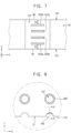
- FIG. 5 is a perspective view illustrating a through-groove test terminal of the inspection pad portion in FIG. 3 .
- FIG. 6 is a plan view illustrating a fourth contact pad of the through-groove test terminal in FIG. 5 .
- FIG. 7 is a front view illustrating the through-groove test terminal in FIG. 5 .
- a module substrate 100 includes a wiring substrate and a through-groove test terminal 312 provided in an inner wall of a through groove 120 of the wiring substrate.
- the through-groove test terminal 312 includes at least one contact pad provided in the inner wall of the through groove 120.
- the module substrate 100 may be interchangeably referred to as the wiring substrate.
- the wiring substrate may include a plurality of stacked insulation layers and conductive patterns provided in the insulation layers, respectively.
- first to fifth insulation layers 110a, 110b, 110c, 110d, 110e may be sequentially stacked on one another.
- the first insulation layer 110a may be a lower cover insulation layer
- the second insulation layer 110b may be a lower insulation layer
- the third insulation layer 110c may be a core layer
- the fourth insulation layer 110d may be an upper insulation layer
- the fifth insulation layer 110e may be an upper cover insulation layer.
- the insulation layer may include an insulating material having a thermosetting resin such as epoxy resin or a thermoplastic resin such as polyimide.
- the insulation layer may include a resin impregnated in a core material such as organic fiber (glass fiber), for example, a prepreg, FR-4, or BT (Bismaleimide Triazine).
- a first conductive pattern 310a may be formed on a lower surface of the second insulation layer 110b, and a second conductive pattern 310b may be formed on an upper surface of the second insulation layer 110b.
- a third conductive pattern 3 10c may be formed on a lower surface of the fourth insulation layer 110d, and a fourth conductive pattern 310d may be formed on an upper surface of the fourth insulation layer 110d.
- the conductive pattern may include a metal material such as copper or aluminum.
- At least one through groove 120 is provided in a first sidewall S1 of the module substrate 100.
- the through groove 120 extends in a thickness direction of the module substrate 100, that is, in the stacking direction of the insulation layers (eg Z direction).
- the through groove 120 has a shape recessed from the first sidewall S1 to the inside.
- the through groove 120 may have a semi-circle or semi-elliptical shape or a trapezoidal shape when viewed in plan view.
- the first to fifth insulation layers 110a, 110b, 110c, 110d, 110e may have first to fifth semicircular holes 120a, 120b, 120c, 120d, 120e provided in sidewalls thereof, respectively.
- the through groove 120 may include the first to fifth semicircular holes 120a, 120b, 120c, 120d, 120e.
- the first conductive pattern 310a may be provided on the lower surface of the second insulation layer 110b to extend toward the inner wall of the through groove 120 in the second direction, and an end portion of the first conductive pattern 310a may be exposed from the inner wall of the through groove 120.
- the end portion of the first conductive pattern 310a exposed from the inner wall of the through groove 120 may be referred to as a first contact pad 312a.
- the first contact pad 312a may be formed integrally with the first conductive pattern 310a.
- a width of the first contact pad 312a may be greater than a width of the first conductive pattern 310a (e.g., a width of a portion other than the end portion of the first conductive pattern 310a). In this case, the first contact pad 312a may extend by a desired (or alternatively, predetermined) length along the inner wall of the second semicircular hole 120b.
- the second conductive pattern 310b may be provided on the upper surface of the second insulation layer 110b to extend toward the inner wall of the through groove 120 in the second direction, and an end portion of the second conductive pattern 310b may be exposed from the inner wall of the through groove 120.
- the end portion of the second conductive pattern 310b exposed from the inner wall of the through groove 120 may be referred to as a second contact pad 312b.
- the second contact pad 312b may be formed integrally with the second conductive pattern 310b.
- a width of the second contact pad 312b may be greater than a width of the second conductive pattern 310b (e.g., a width of a portion other than the end portion of the second conductive pattern 310b).
- the second contact pad 312b may extend by a desired (or alternatively, predetermined) length along the inner wall of the second semicircular hole 120b.
- the third conductive pattern 310c may be provided on the lower surface of the fourth insulation layer 110d to extend toward the inner wall of the through groove 120 in the second direction, and an end portion of the third conductive pattern 310c may be exposed from the inner wall of the through groove 120.
- the end portion of the third conductive pattern 310c exposed from the inner wall of the through groove 120 may be referred to as a third contact pad 312c.
- the third contact pad 312c may be formed integrally with the third conductive pattern 310c.
- a width of the third contact pad 312c may be greater than a width of the third conductive pattern 310c (e.g., a width of a portion other than the end portion of the third conductive pattern 310c).
- the third contact pad 312c may extend by a desired (or alternatively, predetermined) length along the inner wall of the fourth semicircular hole 120d.
- the fourth conductive pattern 310d may be provided on the upper surface of the fourth insulation layer 110d to extend toward the inner wall of the through groove 120 in the second direction, and an end portion of the fourth conductive pattern 310d may be exposed from the inner wall of the through groove 120.
- the end portion of the fourth conductive pattern 310d exposed from the inner wall of the through groove 120 may be referred to as a fourth contact pad 312d.
- the fourth contact pad 312d may be formed integrally with the fourth conductive pattern 310d.
- a width V of the fourth contact pad 312d may be greater than a width W of the fourth conductive pattern 310d (e.g., a width of a portion other than the end portion of the fourth conductive pattern 310d).
- the fourth contact pad 312d may extend by a desired (or alternatively, predetermined) length V along the inner wall of the fourth semicircular hole 120d.
- the through-groove test terminal 312 may include the first to fourth contact pads 312a, 312b, 312c, 312d, a surface of each of which is exposed from the inner wall of the through groove 120.
- the first to fourth contact pads 312a, 312b, 312c, 312d may be spaced apart from each other in the stacking direction.
- a e.g. pogo pin of a tester may be inserted into the through groove 120 to simultaneously contact the first to fourth contact pads 312a, 312b, 312c, 312d.
- the first to fourth conductive patterns 310a, 310b, 310c, 310d may be connected to one via 324.
- the via 324 may be electrically connected to a semiconductor device 200 through a signal line 311. Accordingly, the through-groove test terminal 312 may be electrically connected to the semiconductor device 200 by the via 324 and the signal line 311.
- the through-groove test terminal 312 may be spaced apart by a desired (or alternatively, predetermined) distance D1 from a vertical plane M extending from the first sidewall S1.
- the exposed surfaces of the first to fourth contact pads 312a, 312b, 312c, 312d may be spaced apart from the vertical plane M by the desired (or alternatively, predetermined) distance D1.
- a distance between both end portions of the inner wall of the through groove 120 in contact with the first sidewall S1, that is, a diameter D of the through groove 120 may be within a range of 200 ⁇ m to 800 ⁇ m.
- the spacing distance between the contact pads and the vertical plane M may be within a range of 80 ⁇ m to 320 ⁇ m.
- the through-groove test terminal 312 may be spaced apart by a desired (or alternatively, predetermined) distance D2 from each or either one of first and second horizontal planes N1, N2, the first horizontal plane N1 being a plane extending from the upper surface 102 of the wiring substrate and the second horizontal plane N2 being a plane extending from the lower surface 104 of the wiring substrate.
- the exposed surface of the first contact pad 312a may be spaced apart from the first horizontal plane N1 by the desired (or alternatively, predetermined) distance D2.
- the exposed surface of the fourth contact pad 312d may be spaced apart from the second horizontal plane N2 by the desired (or alternatively, predetermined) distance D2.
- a thickness of the wiring substrate may be within a range of 400 ⁇ m to 1,600 ⁇ m, and the distance between the first contact pad 312a and the first horizontal plane N1 and the distance between the fourth contact pad 312d and the second horizontal plane N2 may be within a range of 50 ⁇ m to 200 ⁇ m.
- the through-groove test terminal 312 may occupy a portion of the inner wall area of the through groove 120.
- the exposed surfaces of the first to fourth contact pads 312a, 312b, 312c, 312d may occupy at least 20% of the inner wall area of the through groove 120.
- the semiconductor module 10 may include a module substrate 100 and a semiconductor device 200 mounted on the module substrate 100.
- the module substrate 100 may include the wiring substrate having the at least one through groove 120 in the sidewall thereof and extending in the thickness direction thereof and the through-groove test terminal 312 having the at least one contact pad exposed from the inner wall of the through groove 120.
- the through-groove test terminal 312 may include the first to fourth contact pads 312a, 312b, 312c, 312d which are provided on the inner wall of the through groove 120 to be spaced apart from each other in the thickness direction of the wiring substrate.
- the through-groove test terminal 312 may be spaced apart by the desired (or alternatively, predetermined) distance D1 from the vertical plane M extending from the first sidewall S1.
- the through-groove test terminal 312 may be spaced apart by the desired (or alternatively, predetermined) distance D2 from the first and second horizontal planes N1 and N2 extending from the upper surface 102 and the lower surface 104 of the wiring substrate.
- interface signal connection terminals for inspection of a semiconductor device may be arranged in the sidewall of the wiring substrate having a small or micro form factor, thereby securing a design space for debug pads. Additionally or alternatively, because in some embodiments copper contact pads are not exposed from the sidewalls of the wiring substrate, it may be possible to improve contact reliability with the inspection e.g. pogo pin while satisfying PCB design regulations.
- FIG. 8 is a plan view illustrating a portion of an inspection pad portion of a memory module in accordance with some example embodiments.
- FIG. 9 is a cross-sectional view taken along the line B-B' in FIG. 8 .
- FIG. 10 is a perspective view illustrating a through-groove test terminal of the inspection pad portion in FIG. 8 .
- FIG. 11 is a plan view illustrating a fourth contact pad and a plating pattern of the through-groove test terminal in FIG. 10 .
- FIG. 12 is a front view illustrating the through-groove test terminal in FIG. 10 .
- the through-groove test terminal may be the same as or substantially similar to the through-groove test terminal described with reference to FIGS. 3 to 7 except for a configuration of an additional plating pattern.
- same reference numerals will be used to refer to the same or like elements and any further repetitive explanation concerning the above elements will be omitted.
- a through-groove test terminal includes at least one contact pad provided in an inner wall of a through groove 120 and a plating pattern 314 on the inner wall of the through groove 120 to cover the contact pad.
- the plating pattern 314 is provided on the inner wall of the through groove 120 and extends by a desired (or alternatively, predetermined) length in a thickness direction (eg Z direction) of a wiring substrate.
- the plating pattern 314 may make contact with exposed surfaces of first to fourth contact pads 312a, 312b, 312c, 312d.
- the plating pattern 314 may cover the exposed surfaces of the first to fourth contact pads 312a, 312b, 312c, 312d and portions of surfaces of second to fourth insulation layers 110b, 110c, 110d therebetween.
- the plating pattern 314 may be electrically connected to first to fourth conductive patterns 310a, 310b, 310c, 310d by the first to fourth contact pads 312a, 312b, 312c, 312d.
- the first to fourth conductive patterns 310a, 310b, 310c, 310d may be connected to one via 324. Accordingly, the through-groove test terminal may be electrically connected to a semiconductor device 200 by the via 324 and a signal line 311.
- a plating layer may be formed on the inner wall of the through groove 120 by an electroplating process, and then the plating layer may be patterned eg by an etching process or a drilling process to form the plating pattern 314.
- the plating pattern may include a metal material such as copper or nickel.
- the plating pattern 314 is spaced apart by a desired (or alternatively, predetermined) distance D3 from a vertical plane M extending from a first sidewall S1.
- the plating pattern 314 has a central angle ⁇ with respect to the center of the through groove 120.
- the central angle ⁇ has an angular range of 30 degrees to 70 degrees.
- a distance between both end portions of the inner wall of the through groove 120 in contact with the first sidewall S1, that is, a diameter D of the through groove 120 may be within a range of 200 ⁇ m to 800 ⁇ m.
- the spacing distance between the plating pattern and the vertical plane M may be within a range of 60 ⁇ m to 300 ⁇ m.
- the plating pattern 314 may be spaced apart by a desired (or alternatively, predetermined) distance D4 from each or either one of first and second horizontal planes N1, N2, the first horizontal plane N1 being a plane extending from an upper surface 102 of the wiring substrate and the second horizontal plane N2 being a plane extending from a lower surface 104 of the wiring substrate.
- a lower surface of the plating pattern 314 may be spaced apart from the first horizontal plane N1 by the distance D4.
- An upper surface of the plating pattern 314 may be spaced apart from the second horizontal plane N2 by the desired (or alternatively, predetermined) distance D4.
- a thickness of the wiring substrate may be within a range of 400 ⁇ m to 1,600 ⁇ m, and/or the distance between the lower surface of the plating pattern 314 and the first horizontal plane N1 and the distance between the upper surface of the plating pattern 314 and the second horizontal plane N2 may be within a range of 50 ⁇ m to 200 ⁇ m.
- the plating pattern 314 occupies a portion of the inner wall area of the through groove 120.
- the plating pattern 314 may occupy at least 40% of the inner wall area of the through groove 120.
- FIG. 13 is a cross-sectional view illustrating a through groove test terminal formed in a wiring substrate in accordance with some example embodiments.
- a through-groove test terminal may include first to fourth contact pads 312a, 312b, 312c, 312d exposed from an inner wall of a through groove 120, and the first to fourth contact pads 312a,312b, 312c, 312d may be connected to first to fourth conductive patterns 310a, 310b, 310c, 310d, respectively.
- the first and second conductive patterns 310a, 310b may be connected to a first via 324a, and the first via 324a may be electrically connected to a semiconductor device 200 through a first signal line 311a.
- the third and fourth conducive patterns 310c, 310d may be connected to a second via 324b, and the second via 324b may be electrically connected to the semiconductor device 200 through a second signal line 311b.
- first and second vias 324a, 324b may include a blind via or a buried via.
- an inspection mode or operation mode may be controlled according to an internal signal connection state of the first to fourth contact pads.
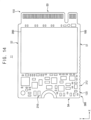
- FIG. 14 is a plan view illustrating a memory module in accordance with some example embodiments.
- the memory module may be the same as or substantially similar to the memory module described with reference to FIG. 1 except for a configuration of an inspection pad portion.
- same reference numerals will be used to refer to the same or like elements and any further repetitive explanation concerning the above elements will be omitted.
- an inspection pad portion 300 of a memory module 11 may be provided in a through groove 120 formed in at least one inner wall of a module substrate 100.
- the inspection pad portion 300 may include through-groove test terminals 312 provided in the through grooves 120, respectively.
- the through-groove test terminal may be the same as or substantially similar to the through-groove test terminal described with reference to FIGS. 3 to 7 .
- test terminals of the inspection pad portion 300 may be provided only in the through grooves 120 formed in the inner wall of a wiring substrate.
- the through grooves 120 may be formed in a first sidewall S1 to be spaced apart from each other along a first direction (eg X direction).
- the through-groove test terminals may be provided on inner walls of the through grooves 120, respectively.
- the inspection pad portion may include 10 through-groove test terminals. However, arrangements and the number of the through-groove test terminals may not be limited thereto.
- test pads are provided only on the sidewalls of the wiring substrate, a design space for electronic components and interface signal connection pads may be secured sufficiently.
- Memory modules according to some example embodiments have been described as being applied to an SSD, but it may not be limited thereto, and the memory module may be implemented as a semiconductor module including a plurality of memory devices.
- the host (or the host system) and the memory module disclosed in the present disclosure may be implemented as processing circuitry such as hardware including logic circuits or a combination of hardware and software such as a processor executing software.
- the processing circuitry may include, but is not limited to, a central processing unit (CPU) , an arithmetic logic unit (ALU), a digital signal processor, a microcomputer, a field programmable gate array (FPGA), a System-on-Chip (SoC), a programmable logic unit, a microprocessor, application-specific integrated circuit (ASIC), etc.
Landscapes
- Engineering & Computer Science (AREA)
- Microelectronics & Electronic Packaging (AREA)
- Manufacturing & Machinery (AREA)
- Printing Elements For Providing Electric Connections Between Printed Circuits (AREA)
Claims (14)
- Modulsubstrat (100) für ein Halbleitermodul (10), umfassend:ein Verdrahtungssubstrat mit einer oberen Fläche (102) und einer unteren Fläche (104), die einander gegenüberliegen und eine Verdrahtung mit mindestens einem darin ausgebildeten leitenden Muster (310a, 310b, 310c, 310d) einschließen, wobei das Verdrahtungssubstrat mindestens eine Durchgangsnut (120) in mindestens einer Seitenwand (S1) aufweist, die sich in Richtung der Dicke erstreckt; undeinen Durchgangsnut-Testanschluss (312), der mindestens ein Kontaktpad (312a, 312b, 312c, 312d) einschließt, wobei das mindestens eine Kontaktpad (312a, 312b, 312c, 312d) einen Endabschnitt des mindestens einen leitenden Musters umfasst und eine Oberfläche des Kontaktpads (312a, 312b, 312c, 312d) von einer Innenwand der Durchgangsnut freigelegt ist,wobei das Kontaktpad von einer vertikalen Ebene (M) beabstandet ist, die sich von der Seitenwand des Verdrahtungssubstrats aus erstreckt, und dadurch gekennzeichnet, dass der Durchgangsnut-Testanschluss (312) ferner ein Plattierungsmuster (314) auf der Innenwand der Durchgangsnut einschließt, wobei das Plattierungsmuster (314) so konfiguriert ist, dass es die freiliegende Oberfläche des Kontaktpads (312a, 312b, 312c, 312d) abdeckt und von der vertikalen Ebene um einen Abstand (D3) beabstandet ist, wobei das Plattierungsmuster einen Winkel (θ) bildet, der in Bezug auf eine Mitte der Durchgangsnut zentriert ist, wobei der Winkel (θ) einen Winkelbereich von 30 Grad bis 70 Grad aufweist.
- Modulsubstrat für das Halbleitermodul nach Anspruch 1, wobei das Verdrahtungssubstrat eine Vielzahl von gestapelten Isolationsschichten (110a, 110b, 110c, 110d, 110e), eine Vielzahl von leitenden Mustern, die jeweils auf den Isolationsschichten bereitgestellt sind, und eine Vielzahl von Kontaktpads einschließt, die jeweils mit den leitenden Mustern elektrisch verbunden sind.
- Modulsubstrat für das Halbleitermodul nach Anspruch 2, wobei die Kontaktpads entlang der Stapelrichtung der Isolationsschichten voneinander beabstandet sind.
- Modulsubstrat für das Halbleitermodul nach Anspruch 2 oder 3, wobei eine Vielzahl der Kontaktpads mindestens 20 % einer Fläche der Innenwand der Durchgangsnut einnimmt.
- Modulsubstrat für das Halbleitermodul nach einem der vorhergehenden Ansprüche, wobei das Kontaktpad eine Vielzahl von Kontaktpads umfasst, wobei die Kontaktpads jeweils mit einer Vielzahl von leitenden Mustern elektrisch verbunden sind und das Plattierungsmuster Oberflächen der Kontaktpads abdeckt.
- Modulsubstrat für das Halbleitermodul nach einem der vorhergehenden Ansprüche, wobei das Plattierungsmuster mindestens 40 % einer Fläche der Innenwand der Durchgangsnut einnimmt.
- Modulsubstrat für das Halbleitermodul nach einem der vorhergehenden Ansprüche, wobei ein erster Abstand (D) zwischen den beiden Endabschnitten der Innenwand der Durchgangsnut, die mit der Seitenwand in Kontakt sind, in einem Bereich von 200 µm bis 800 µm liegt und ein zweiter Abstand (D1) zwischen dem Kontaktpad und der vertikalen Ebene in einem Bereich von 80 µm bis 320 µm liegt.
- Modulsubstrat für das Halbleitermodul nach einem der vorhergehenden Ansprüche, wobei das Kontaktpad von einer horizontalen Ebene (N1, N2), die sich von der oberen Oberfläche oder der unteren Oberfläche des Verdrahtungssubstrats erstreckt, um einen Abstand (D2) beabstandet ist.
- Modulsubstrat für das Halbleitermodul nach Anspruch 8, wobei eine Dicke des Verdrahtungssubstrats in einem Bereich von 400 µm bis 1 600 µm liegt und der Abstand zwischen dem Kontaktpad und der horizontalen Ebene in einem Bereich von 50 µm bis 200 µm liegt.
- Modulsubstrat für das Halbleitermodul nach einem der vorhergehenden Ansprüche,wobei das Verdrahtungssubstrat eine erste bis fünfte Isolationsschicht und ein erstes bis viertes leitendes Muster zwischen der ersten bis fünften Isolationsschicht einschließt, wobei sich die Durchgangsnut in der mindestens einen Seitenwand des Verdrahtungssubstrats in einer Stapelrichtung der ersten bis fünften Isolationsschicht erstreckt; undwobei der Durchgangsnut-Testanschluss ein erstes bis viertes Kontaktpad einschließt, wobei das erste bis vierte Kontaktpad jeweils mit dem ersten bis vierten leitenden Muster elektrisch verbunden ist, wobei Oberflächen des ersten bis vierten Kontaktpads von einer Innenwand der Durchgangsnut aus freigelegt sind,wobei das erste bis vierte Kontaktpad von der vertikalen Ebene, die sich von der Seitenwand des Verdrahtungssubstrats erstreckt, beabstandet ist, undwobei ein zweiter Abstand zwischen jedem des ersten bis vierten Kontaktpads und der vertikalen Ebene innerhalb eines Bereichs von 80 µm bis 320 µm liegt.
- Modulsubstrat für das Halbleitermodul nach Anspruch 10, wobei der Durchgangsnut-Testanschluss ferner ein Plattierungsmuster auf der Innenwand der Durchgangsnut einschließt, wobei das Plattierungsmuster so konfiguriert ist, dass es die freiliegenden Oberflächen des ersten bis vierten Kontaktpads abdeckt und von der vertikalen Ebene um einen dritten Abstand beabstandet ist.
- Modulsubstrat für das Halbleitermodul nach Anspruch 10 oder 11, wobei das erste bis vierte leitende Muster mit einer Durchkontaktierung (324) verbunden sind, die mindestens einen Teil des Verdrahtungssubstrats durchdringt.
- Modulsubstrat für das Halbleitermodul nach einem der Ansprüche 10 bis 12, wobei einige des ersten bis vierten leitenden Musters mit einer ersten Durchkontaktierung (324a) verbunden sind, die mindestens einen Teil des Verdrahtungssubstrats durchdringt, und andere des ersten bis vierten leitenden Musters mit einer zweiten Durchkontaktierung (324b) verbunden sind, die einen anderen Teil des Verdrahtungssubstrats durchdringt.
- Modulsubstrat für das Halbleitermodul nach einem der vorhergehenden Ansprüchen, wobei das mindestens eine Kontaktpad einstückig mit dem mindestens einen leitenden Muster ausgebildet ist.
Applications Claiming Priority (1)
| Application Number | Priority Date | Filing Date | Title |
|---|---|---|---|
| KR1020200135836A KR102867266B1 (ko) | 2020-10-20 | 2020-10-20 | 모듈 기판 및 이를 포함하는 반도체 모듈 |
Publications (2)
| Publication Number | Publication Date |
|---|---|
| EP3989683A1 EP3989683A1 (de) | 2022-04-27 |
| EP3989683B1 true EP3989683B1 (de) | 2023-09-20 |
Family
ID=77358083
Family Applications (1)
| Application Number | Title | Priority Date | Filing Date |
|---|---|---|---|
| EP21187443.3A Active EP3989683B1 (de) | 2020-10-20 | 2021-07-23 | Modulsubstrat und halbleitermodul damit |
Country Status (4)
| Country | Link |
|---|---|
| US (2) | US11490509B2 (de) |
| EP (1) | EP3989683B1 (de) |
| KR (1) | KR102867266B1 (de) |
| CN (1) | CN114390768A (de) |
Family Cites Families (13)
| Publication number | Priority date | Publication date | Assignee | Title |
|---|---|---|---|---|
| JPH10247766A (ja) | 1997-03-03 | 1998-09-14 | Alps Electric Co Ltd | 回路基板 |
| JP2003338672A (ja) | 2002-05-21 | 2003-11-28 | Daisho Denshi:Kk | プリント配線板 |
| JP2005223266A (ja) | 2004-02-09 | 2005-08-18 | Sharp Corp | 基板の端面スルーホール製造方法 |
| KR100654085B1 (ko) | 2005-08-09 | 2006-12-06 | 주식회사 신화테크 | 다층 인쇄회로기판의 슬루프형 스루홀 제조공법 |
| KR100723529B1 (ko) * | 2006-05-10 | 2007-05-30 | 삼성전자주식회사 | 홀을 갖는 솔더볼 랜드를 구비하는 회로기판 및 이를구비하는 반도체 패키지 |
| JP4331769B2 (ja) * | 2007-02-28 | 2009-09-16 | Tdk株式会社 | 配線構造及びその形成方法並びにプリント配線板 |
| US7741709B2 (en) | 2008-01-09 | 2010-06-22 | Inpaq Technology Co., Ltd. | Embedded type multifunctional integrated structure for integrating protection components and method for manufacturing the same |
| KR20100041515A (ko) | 2008-10-14 | 2010-04-22 | 삼성전자주식회사 | 제거 가능한 보조 검사단자를 갖는 솔리드 스테이트 드라이브의 검사방법 |
| JP2015053363A (ja) | 2013-09-06 | 2015-03-19 | 京セラサーキットソリューションズ株式会社 | 印刷配線板の製造方法 |
| JP6316609B2 (ja) * | 2014-02-05 | 2018-04-25 | 新光電気工業株式会社 | 配線基板及び半導体装置と配線基板の製造方法及び半導体装置の製造方法 |
| KR20160018921A (ko) * | 2014-08-07 | 2016-02-18 | 삼성전자주식회사 | 반도체 메모리 장치 및 그 제조 방법 |
| US10535938B2 (en) * | 2017-03-10 | 2020-01-14 | Tag-Connet, Llc | Side-edge connector system providing electrical connection between devices in a manner which minimizes dedicated connection space |
| US10791632B1 (en) | 2019-09-20 | 2020-09-29 | Raytheon Company | Extremely low profile electrical interconnect for printed wiring board |
-
2020
- 2020-10-20 KR KR1020200135836A patent/KR102867266B1/ko active Active
-
2021
- 2021-06-25 US US17/358,800 patent/US11490509B2/en active Active
- 2021-07-23 EP EP21187443.3A patent/EP3989683B1/de active Active
- 2021-09-24 CN CN202111124136.XA patent/CN114390768A/zh active Pending
-
2022
- 2022-08-30 US US17/898,907 patent/US11792921B2/en active Active
Also Published As
| Publication number | Publication date |
|---|---|
| US11792921B2 (en) | 2023-10-17 |
| US11490509B2 (en) | 2022-11-01 |
| CN114390768A (zh) | 2022-04-22 |
| EP3989683A1 (de) | 2022-04-27 |
| KR20220052011A (ko) | 2022-04-27 |
| US20220124904A1 (en) | 2022-04-21 |
| KR102867266B1 (ko) | 2025-10-01 |
| US20220418097A1 (en) | 2022-12-29 |
Similar Documents
| Publication | Publication Date | Title |
|---|---|---|
| US10204661B2 (en) | Semiconductor device | |
| US9768536B2 (en) | Socket with routed contacts | |
| US20060049512A1 (en) | Thin module system and method with skew reduction | |
| KR100834826B1 (ko) | 취급손상을 줄인 집적회로 모듈의 구조 및 모듈의 종단저항 배치방법 | |
| EP2973698B1 (de) | Verfahren zur herstellung eines stapelspeichergehäuses und pinbelegungs-design für ein ic-gehäuse-substrat | |
| US11277916B2 (en) | Memory system and storage device including printed circuit board with subset of channels arranged in point-to-point topology and subset of channels arranged in daisy-chain topology | |
| US9024426B2 (en) | Semiconductor device and method of manufacturing the same | |
| US12267957B2 (en) | Hybrid pitch through hole connector | |
| KR20130097481A (ko) | 인쇄회로기판(pcb) 및 그 pcb를 포함한 메모리 모듈 | |
| US8093708B2 (en) | Semiconductor package having non-uniform contact arrangement | |
| US8422236B2 (en) | Pin module and chip on board type use device | |
| US20170109098A1 (en) | Semiconductor device | |
| US11792921B2 (en) | Module substrate and semiconductor module including the same | |
| US12295095B2 (en) | Printed circuit board and storage device including the same | |
| US9888565B2 (en) | Memory module and solid state drive having the same | |
| US10242716B2 (en) | Semiconductor device having a slit for aligning a connector and a hole for determining positional accuracy of the slit | |
| KR20100115268A (ko) | 솔리드 스테이트 드라이브 | |
| US20170105282A1 (en) | Circuit board structure | |
| US9543271B2 (en) | Semiconductor device having a sealing layer covering a semiconductor memory unit and a memory controller | |
| US12463140B2 (en) | Flexible interposer for semiconductor dies | |
| KR102888554B1 (ko) | 반도체 모듈용 모듈 기판, 반도체 모듈 및 이를 테스트하기 위한 테스트 소켓 | |
| US12520424B2 (en) | Semiconductor storage device | |
| US20250098068A1 (en) | Semiconductor storage device and semiconductor storage unit | |
| US20260114280A1 (en) | Memory device | |
| TWM657395U (zh) | 電路板組件及主機設備 |
Legal Events
| Date | Code | Title | Description |
|---|---|---|---|
| PUAI | Public reference made under article 153(3) epc to a published international application that has entered the european phase |
Free format text: ORIGINAL CODE: 0009012 |
|
| STAA | Information on the status of an ep patent application or granted ep patent |
Free format text: STATUS: REQUEST FOR EXAMINATION WAS MADE |
|
| 17P | Request for examination filed |
Effective date: 20210723 |
|
| AK | Designated contracting states |
Kind code of ref document: A1 Designated state(s): AL AT BE BG CH CY CZ DE DK EE ES FI FR GB GR HR HU IE IS IT LI LT LU LV MC MK MT NL NO PL PT RO RS SE SI SK SM TR |
|
| STAA | Information on the status of an ep patent application or granted ep patent |
Free format text: STATUS: EXAMINATION IS IN PROGRESS |
|
| 17Q | First examination report despatched |
Effective date: 20220913 |
|
| GRAP | Despatch of communication of intention to grant a patent |
Free format text: ORIGINAL CODE: EPIDOSNIGR1 |
|
| STAA | Information on the status of an ep patent application or granted ep patent |
Free format text: STATUS: GRANT OF PATENT IS INTENDED |
|
| RIC1 | Information provided on ipc code assigned before grant |
Ipc: H05K 3/42 20060101ALN20230323BHEP Ipc: H05K 1/11 20060101ALN20230323BHEP Ipc: H05K 3/40 20060101ALI20230323BHEP Ipc: H05K 1/02 20060101AFI20230323BHEP |
|
| INTG | Intention to grant announced |
Effective date: 20230404 |
|
| P01 | Opt-out of the competence of the unified patent court (upc) registered |
Effective date: 20230519 |
|
| GRAS | Grant fee paid |
Free format text: ORIGINAL CODE: EPIDOSNIGR3 |
|
| GRAA | (expected) grant |
Free format text: ORIGINAL CODE: 0009210 |
|
| STAA | Information on the status of an ep patent application or granted ep patent |
Free format text: STATUS: THE PATENT HAS BEEN GRANTED |
|
| AK | Designated contracting states |
Kind code of ref document: B1 Designated state(s): AL AT BE BG CH CY CZ DE DK EE ES FI FR GB GR HR HU IE IS IT LI LT LU LV MC MK MT NL NO PL PT RO RS SE SI SK SM TR |
|
| REG | Reference to a national code |
Ref country code: GB Ref legal event code: FG4D |
|
| REG | Reference to a national code |
Ref country code: CH Ref legal event code: EP |
|
| REG | Reference to a national code |
Ref country code: DE Ref legal event code: R096 Ref document number: 602021005247 Country of ref document: DE |
|
| REG | Reference to a national code |
Ref country code: IE Ref legal event code: FG4D |
|
| REG | Reference to a national code |
Ref country code: LT Ref legal event code: MG9D |
|
| PG25 | Lapsed in a contracting state [announced via postgrant information from national office to epo] |
Ref country code: GR Free format text: LAPSE BECAUSE OF FAILURE TO SUBMIT A TRANSLATION OF THE DESCRIPTION OR TO PAY THE FEE WITHIN THE PRESCRIBED TIME-LIMIT Effective date: 20231221 |
|
| REG | Reference to a national code |
Ref country code: NL Ref legal event code: MP Effective date: 20230920 |
|
| PG25 | Lapsed in a contracting state [announced via postgrant information from national office to epo] |
Ref country code: SE Free format text: LAPSE BECAUSE OF FAILURE TO SUBMIT A TRANSLATION OF THE DESCRIPTION OR TO PAY THE FEE WITHIN THE PRESCRIBED TIME-LIMIT Effective date: 20230920 Ref country code: RS Free format text: LAPSE BECAUSE OF FAILURE TO SUBMIT A TRANSLATION OF THE DESCRIPTION OR TO PAY THE FEE WITHIN THE PRESCRIBED TIME-LIMIT Effective date: 20230920 Ref country code: NO Free format text: LAPSE BECAUSE OF FAILURE TO SUBMIT A TRANSLATION OF THE DESCRIPTION OR TO PAY THE FEE WITHIN THE PRESCRIBED TIME-LIMIT Effective date: 20231220 Ref country code: LV Free format text: LAPSE BECAUSE OF FAILURE TO SUBMIT A TRANSLATION OF THE DESCRIPTION OR TO PAY THE FEE WITHIN THE PRESCRIBED TIME-LIMIT Effective date: 20230920 Ref country code: LT Free format text: LAPSE BECAUSE OF FAILURE TO SUBMIT A TRANSLATION OF THE DESCRIPTION OR TO PAY THE FEE WITHIN THE PRESCRIBED TIME-LIMIT Effective date: 20230920 Ref country code: HR Free format text: LAPSE BECAUSE OF FAILURE TO SUBMIT A TRANSLATION OF THE DESCRIPTION OR TO PAY THE FEE WITHIN THE PRESCRIBED TIME-LIMIT Effective date: 20230920 Ref country code: GR Free format text: LAPSE BECAUSE OF FAILURE TO SUBMIT A TRANSLATION OF THE DESCRIPTION OR TO PAY THE FEE WITHIN THE PRESCRIBED TIME-LIMIT Effective date: 20231221 Ref country code: FI Free format text: LAPSE BECAUSE OF FAILURE TO SUBMIT A TRANSLATION OF THE DESCRIPTION OR TO PAY THE FEE WITHIN THE PRESCRIBED TIME-LIMIT Effective date: 20230920 |
|
| REG | Reference to a national code |
Ref country code: AT Ref legal event code: MK05 Ref document number: 1614436 Country of ref document: AT Kind code of ref document: T Effective date: 20230920 |
|
| PG25 | Lapsed in a contracting state [announced via postgrant information from national office to epo] |
Ref country code: NL Free format text: LAPSE BECAUSE OF FAILURE TO SUBMIT A TRANSLATION OF THE DESCRIPTION OR TO PAY THE FEE WITHIN THE PRESCRIBED TIME-LIMIT Effective date: 20230920 |
|
| PG25 | Lapsed in a contracting state [announced via postgrant information from national office to epo] |
Ref country code: IS Free format text: LAPSE BECAUSE OF FAILURE TO SUBMIT A TRANSLATION OF THE DESCRIPTION OR TO PAY THE FEE WITHIN THE PRESCRIBED TIME-LIMIT Effective date: 20240120 |
|
| PG25 | Lapsed in a contracting state [announced via postgrant information from national office to epo] |
Ref country code: AT Free format text: LAPSE BECAUSE OF FAILURE TO SUBMIT A TRANSLATION OF THE DESCRIPTION OR TO PAY THE FEE WITHIN THE PRESCRIBED TIME-LIMIT Effective date: 20230920 |
|
| PG25 | Lapsed in a contracting state [announced via postgrant information from national office to epo] |
Ref country code: ES Free format text: LAPSE BECAUSE OF FAILURE TO SUBMIT A TRANSLATION OF THE DESCRIPTION OR TO PAY THE FEE WITHIN THE PRESCRIBED TIME-LIMIT Effective date: 20230920 |
|
| PG25 | Lapsed in a contracting state [announced via postgrant information from national office to epo] |
Ref country code: SM Free format text: LAPSE BECAUSE OF FAILURE TO SUBMIT A TRANSLATION OF THE DESCRIPTION OR TO PAY THE FEE WITHIN THE PRESCRIBED TIME-LIMIT Effective date: 20230920 Ref country code: RO Free format text: LAPSE BECAUSE OF FAILURE TO SUBMIT A TRANSLATION OF THE DESCRIPTION OR TO PAY THE FEE WITHIN THE PRESCRIBED TIME-LIMIT Effective date: 20230920 Ref country code: IS Free format text: LAPSE BECAUSE OF FAILURE TO SUBMIT A TRANSLATION OF THE DESCRIPTION OR TO PAY THE FEE WITHIN THE PRESCRIBED TIME-LIMIT Effective date: 20240120 Ref country code: ES Free format text: LAPSE BECAUSE OF FAILURE TO SUBMIT A TRANSLATION OF THE DESCRIPTION OR TO PAY THE FEE WITHIN THE PRESCRIBED TIME-LIMIT Effective date: 20230920 Ref country code: EE Free format text: LAPSE BECAUSE OF FAILURE TO SUBMIT A TRANSLATION OF THE DESCRIPTION OR TO PAY THE FEE WITHIN THE PRESCRIBED TIME-LIMIT Effective date: 20230920 Ref country code: CZ Free format text: LAPSE BECAUSE OF FAILURE TO SUBMIT A TRANSLATION OF THE DESCRIPTION OR TO PAY THE FEE WITHIN THE PRESCRIBED TIME-LIMIT Effective date: 20230920 Ref country code: AT Free format text: LAPSE BECAUSE OF FAILURE TO SUBMIT A TRANSLATION OF THE DESCRIPTION OR TO PAY THE FEE WITHIN THE PRESCRIBED TIME-LIMIT Effective date: 20230920 Ref country code: SK Free format text: LAPSE BECAUSE OF FAILURE TO SUBMIT A TRANSLATION OF THE DESCRIPTION OR TO PAY THE FEE WITHIN THE PRESCRIBED TIME-LIMIT Effective date: 20230920 Ref country code: PT Free format text: LAPSE BECAUSE OF FAILURE TO SUBMIT A TRANSLATION OF THE DESCRIPTION OR TO PAY THE FEE WITHIN THE PRESCRIBED TIME-LIMIT Effective date: 20240122 |
|
| PG25 | Lapsed in a contracting state [announced via postgrant information from national office to epo] |
Ref country code: PL Free format text: LAPSE BECAUSE OF FAILURE TO SUBMIT A TRANSLATION OF THE DESCRIPTION OR TO PAY THE FEE WITHIN THE PRESCRIBED TIME-LIMIT Effective date: 20230920 Ref country code: IT Free format text: LAPSE BECAUSE OF FAILURE TO SUBMIT A TRANSLATION OF THE DESCRIPTION OR TO PAY THE FEE WITHIN THE PRESCRIBED TIME-LIMIT Effective date: 20230920 |
|
| REG | Reference to a national code |
Ref country code: DE Ref legal event code: R097 Ref document number: 602021005247 Country of ref document: DE |
|
| PG25 | Lapsed in a contracting state [announced via postgrant information from national office to epo] |
Ref country code: DK Free format text: LAPSE BECAUSE OF FAILURE TO SUBMIT A TRANSLATION OF THE DESCRIPTION OR TO PAY THE FEE WITHIN THE PRESCRIBED TIME-LIMIT Effective date: 20230920 |
|
| PLBE | No opposition filed within time limit |
Free format text: ORIGINAL CODE: 0009261 |
|
| STAA | Information on the status of an ep patent application or granted ep patent |
Free format text: STATUS: NO OPPOSITION FILED WITHIN TIME LIMIT |
|
| PG25 | Lapsed in a contracting state [announced via postgrant information from national office to epo] |
Ref country code: DK Free format text: LAPSE BECAUSE OF FAILURE TO SUBMIT A TRANSLATION OF THE DESCRIPTION OR TO PAY THE FEE WITHIN THE PRESCRIBED TIME-LIMIT Effective date: 20230920 |
|
| 26N | No opposition filed |
Effective date: 20240621 |
|
| PG25 | Lapsed in a contracting state [announced via postgrant information from national office to epo] |
Ref country code: SI Free format text: LAPSE BECAUSE OF FAILURE TO SUBMIT A TRANSLATION OF THE DESCRIPTION OR TO PAY THE FEE WITHIN THE PRESCRIBED TIME-LIMIT Effective date: 20230920 |
|
| PG25 | Lapsed in a contracting state [announced via postgrant information from national office to epo] |
Ref country code: SI Free format text: LAPSE BECAUSE OF FAILURE TO SUBMIT A TRANSLATION OF THE DESCRIPTION OR TO PAY THE FEE WITHIN THE PRESCRIBED TIME-LIMIT Effective date: 20230920 |
|
| PG25 | Lapsed in a contracting state [announced via postgrant information from national office to epo] |
Ref country code: BG Free format text: LAPSE BECAUSE OF FAILURE TO SUBMIT A TRANSLATION OF THE DESCRIPTION OR TO PAY THE FEE WITHIN THE PRESCRIBED TIME-LIMIT Effective date: 20230920 |
|
| PG25 | Lapsed in a contracting state [announced via postgrant information from national office to epo] |
Ref country code: BG Free format text: LAPSE BECAUSE OF FAILURE TO SUBMIT A TRANSLATION OF THE DESCRIPTION OR TO PAY THE FEE WITHIN THE PRESCRIBED TIME-LIMIT Effective date: 20230920 |
|
| PG25 | Lapsed in a contracting state [announced via postgrant information from national office to epo] |
Ref country code: MC Free format text: LAPSE BECAUSE OF FAILURE TO SUBMIT A TRANSLATION OF THE DESCRIPTION OR TO PAY THE FEE WITHIN THE PRESCRIBED TIME-LIMIT Effective date: 20230920 |
|
| REG | Reference to a national code |
Ref country code: CH Ref legal event code: PL |
|
| PG25 | Lapsed in a contracting state [announced via postgrant information from national office to epo] |
Ref country code: LU Free format text: LAPSE BECAUSE OF NON-PAYMENT OF DUE FEES Effective date: 20240723 |
|
| PG25 | Lapsed in a contracting state [announced via postgrant information from national office to epo] |
Ref country code: LU Free format text: LAPSE BECAUSE OF NON-PAYMENT OF DUE FEES Effective date: 20240723 |
|
| PG25 | Lapsed in a contracting state [announced via postgrant information from national office to epo] |
Ref country code: CH Free format text: LAPSE BECAUSE OF NON-PAYMENT OF DUE FEES Effective date: 20240731 Ref country code: BE Free format text: LAPSE BECAUSE OF NON-PAYMENT OF DUE FEES Effective date: 20240731 |
|
| PG25 | Lapsed in a contracting state [announced via postgrant information from national office to epo] |
Ref country code: FR Free format text: LAPSE BECAUSE OF NON-PAYMENT OF DUE FEES Effective date: 20240731 |
|
| REG | Reference to a national code |
Ref country code: BE Ref legal event code: MM Effective date: 20240731 |
|
| PGFP | Annual fee paid to national office [announced via postgrant information from national office to epo] |
Ref country code: GB Payment date: 20250529 Year of fee payment: 5 |
|
| PG25 | Lapsed in a contracting state [announced via postgrant information from national office to epo] |
Ref country code: IE Free format text: LAPSE BECAUSE OF NON-PAYMENT OF DUE FEES Effective date: 20240723 |
|
| PGFP | Annual fee paid to national office [announced via postgrant information from national office to epo] |
Ref country code: DE Payment date: 20250528 Year of fee payment: 5 |
|
| PG25 | Lapsed in a contracting state [announced via postgrant information from national office to epo] |
Ref country code: CY Free format text: LAPSE BECAUSE OF FAILURE TO SUBMIT A TRANSLATION OF THE DESCRIPTION OR TO PAY THE FEE WITHIN THE PRESCRIBED TIME-LIMIT; INVALID AB INITIO Effective date: 20210723 |
|
| PG25 | Lapsed in a contracting state [announced via postgrant information from national office to epo] |
Ref country code: HU Free format text: LAPSE BECAUSE OF FAILURE TO SUBMIT A TRANSLATION OF THE DESCRIPTION OR TO PAY THE FEE WITHIN THE PRESCRIBED TIME-LIMIT; INVALID AB INITIO Effective date: 20210723 |