EP3989397B1 - Circuit de détection d'objets étrangers pour systèmes de transmission de puissance sans fil - Google Patents
Circuit de détection d'objets étrangers pour systèmes de transmission de puissance sans fil Download PDFInfo
- Publication number
- EP3989397B1 EP3989397B1 EP21198160.0A EP21198160A EP3989397B1 EP 3989397 B1 EP3989397 B1 EP 3989397B1 EP 21198160 A EP21198160 A EP 21198160A EP 3989397 B1 EP3989397 B1 EP 3989397B1
- Authority
- EP
- European Patent Office
- Prior art keywords
- wireless power
- power circuit
- factor
- coupled
- circuit
- Prior art date
- Legal status (The legal status is an assumption and is not a legal conclusion. Google has not performed a legal analysis and makes no representation as to the accuracy of the status listed.)
- Active
Links
Images


Classifications
-
- H—ELECTRICITY
- H02—GENERATION; CONVERSION OR DISTRIBUTION OF ELECTRIC POWER
- H02J—CIRCUIT ARRANGEMENTS OR SYSTEMS FOR SUPPLYING OR DISTRIBUTING ELECTRIC POWER; SYSTEMS FOR STORING ELECTRIC ENERGY
- H02J50/00—Circuit arrangements or systems for wireless supply or distribution of electric power
- H02J50/60—Circuit arrangements or systems for wireless supply or distribution of electric power responsive to the presence of foreign objects, e.g. detection of living beings
-
- H—ELECTRICITY
- H02—GENERATION; CONVERSION OR DISTRIBUTION OF ELECTRIC POWER
- H02J—CIRCUIT ARRANGEMENTS OR SYSTEMS FOR SUPPLYING OR DISTRIBUTING ELECTRIC POWER; SYSTEMS FOR STORING ELECTRIC ENERGY
- H02J50/00—Circuit arrangements or systems for wireless supply or distribution of electric power
- H02J50/10—Circuit arrangements or systems for wireless supply or distribution of electric power using inductive coupling
- H02J50/12—Circuit arrangements or systems for wireless supply or distribution of electric power using inductive coupling of the resonant type
-
- Y—GENERAL TAGGING OF NEW TECHNOLOGICAL DEVELOPMENTS; GENERAL TAGGING OF CROSS-SECTIONAL TECHNOLOGIES SPANNING OVER SEVERAL SECTIONS OF THE IPC; TECHNICAL SUBJECTS COVERED BY FORMER USPC CROSS-REFERENCE ART COLLECTIONS [XRACs] AND DIGESTS
- Y02—TECHNOLOGIES OR APPLICATIONS FOR MITIGATION OR ADAPTATION AGAINST CLIMATE CHANGE
- Y02B—CLIMATE CHANGE MITIGATION TECHNOLOGIES RELATED TO BUILDINGS, e.g. HOUSING, HOUSE APPLIANCES OR RELATED END-USER APPLICATIONS
- Y02B70/00—Technologies for an efficient end-user side electric power management and consumption
- Y02B70/10—Technologies improving the efficiency by using switched-mode power supplies [SMPS], i.e. efficient power electronics conversion e.g. power factor correction or reduction of losses in power supplies or efficient standby modes
Definitions
- This disclosure is related to the field of wireless power transmission and, in particular, to a foreign objection detection sensing circuit for wireless power transmission systems.
- Portable electronic devices such as smartphones, smartwatches, audio output devices (earbuds, headphones), and wearables operate on battery power, not from wired power transmitted thereto over wired transmission lines and distribution systems.
- the batteries used for such devices are typically rechargeable and, therefore, a way to recharge the power of such batteries is necessary.
- Most portable electronic devices include a charging port, typically conforming to the Micro USB or USB-C standards, into which a power cord connected to a power source can be inserted to provide for recharging of their batteries.
- a charging port typically conforming to the Micro USB or USB-C standards
- such charging ports may make it difficult to enhance the water resistance of the electronic device, and are subject to damage from repeated use.
- some smaller portable electronic devices for example, earbuds and smartwatches
- some users may find it cumbersome to plug a power cord into the charging port of an electronic device to charge the battery of that device.
- a wireless power transmission system 10 may be comprised of a first device 11 and a second device 15.
- the first device 11 may be a device capable of wireless power transmission (for example, a smartphone) and/or wireless power reception (for example, a device to be wirelessly charged, such as a charging case for a pair of wireless earbuds or an active stylus), and the second device 15 may be a device capable of both wireless power transmission and wireless power reception, such as a smartphone.
- the first device 11 includes a coil Ls (considered to be a secondary when receiving power; the capacitance Cs represents a tuning capacitance for the coil Ls) in which a time-varying current is induced by a time-varying electric field when receiving power, and hardware 12 that rectifies, regulates, and makes use of the time-varying current induced in the coil Ls to provide power to the device 11, for example to charge its battery.
- a coil Ls considered to be a secondary when receiving power; the capacitance Cs represents a tuning capacitance for the coil Ls
- hardware 12 that rectifies, regulates, and makes use of the time-varying current induced in the coil Ls to provide power to the device 11, for example to charge its battery.
- the second device 15 includes a controlled switching bridge circuit (operable as either a bridge rectifier or a DC-AC inverter) 16 coupled to a transceiver coil Lxcvr at nodes Ac1 and Ac2, with a discrete capacitor Cxcvr being used to tune the second device 15.
- the controlled switching bridge circuit 16 is comprised of transistors T1-T4 controlled by gate voltages G1-G4.
- a tank capacitor Ctank is coupled between node Nin and node N.
- a voltage regulator 17 has an input coupled to node Nin and an output coupled to node Nout.
- a battery 18 is selectively coupled between node Nout and node N by a switch SW1, and is selectively coupled between the node N and node Nin by a switch SW2.
- the switches SW1 and SW2 operate out of phase with one another; switch SW1 is closed while switch SW2 is opened when the second device 15 operates as a receiver in a power reception mode with the circuit 16 functioning as an AC-DC rectifier and the regulator functioning to generate the regulated voltage Vreg for charging the battery of the second device 15, and switch SW1 is opened while switch SW2 is closed when the second device 15 operates as a transmitter in a power transmission mode with the circuit 16 functioning as a DC-AC inverter powered by the battery 18 in a mode to transfer power supplied by battery 18 to the first device 11.
- a controller 19 generates the gate voltages G1-G4 for controlling the bridge 16 to operate in the desired rectifier/inverter mode.
- the controlled switching bridge circuit 16 rectifies the AC current flowing in transceiver coil Lxcvr to produce a DC current that charges the tank capacitor Ctank connected to the node Nin, and a rectified voltage Vrect is formed across the tank capacitor Ctank.
- the voltage regulator 17 produces a regulated output voltage Vreg at its output node Nout from that rectified voltage Vrect, which is provided to the battery 18 to thereby charge the battery 18.
- the voltage of the battery 18 is applied to the node Nin by switch SW2 and becomes the voltage Vrect. Then, the gate voltages G1-G4 are driven by the controller 19 so as to generate a time-varying current flowing through the transceiver coil Lxcvr.
- a conductive foreign object 20 may inadvertently be physically present between the first device 11 and second device 15, such as shown in FIG. 2 .
- foreign objects are electrically-conductive materials that are placed in the field, such as coins, keys, paperclips, etc., and that are not part of the wireless charging system and are not protected by the shielding in either the transmitting or receiving device.
- the alternating magnetic field between a transmitter and a receiver can induce eddy currents in these electrically conductive materials that are exposed to the field, the eddy currents cause those materials to heat up. Therefore, it is desired for these objects to be detected and removed from a wireless power transmission system for efficient power deliver and safety of operation.
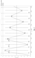
- the quality factor (Q-factor) of the second device 15, an indication of the efficiency of the power transferred thereto or thereby, may be measured by exciting with the time-varying electric field generated by the transceiver 15 while measuring the peak voltage developed at the node AC1, and then next damped peak voltage at same node AC1.
- a Q-factor sensing block 9 is coupled to the coil Lxcvr. Q-factor measurement cycles may be interleaved with power transmission/reception cycles, but do not occur simultaneously.
- the second device 15 can infer the condition of the system 10.
- Possible relevant conditions of the system 10, when the second device 15 is acting as a transmitter include: (i) both the first device 11 and the second device 15 being in proximity to one another, but not a foreign object 20, (ii) the second device 15 being in proximity to the foreign object 20 but not the first device 11, (iii) the second device 15 being in proximity to neither the first device 11 nor the foreign object 20, and (iv) both the first device 11 and the second device 15 being in proximity to one another as well as to the foreign object 20.
- Q-factor curves for these different system conditions can be inferred. For example, with additional reference to FIG. 3 , in case (i), the resonance amplitude of the coil Lxcvr will be higher than in other conditions and the resonance frequency of the system 10 will be lower than in other conditions, as illustrated in the Q-factor curve labeled as Fr_tx+rx. Similarly, in case (ii), the resonance amplitude of the coil Lxcvr is lower than in other conditions, and the resonance frequency of the system 10 is higher than in other conditions, as illustrated in the Q-factor curve labeled as Fr_tx+fo.
- the resonance amplitude of the coil Lxcvr is less than in case (i) but greater than in case (iii) while the resonance frequency of the coil Lxcvr is greater than in case (i) but less than in case (iii), as illustrated in the Q-factor curve labeled as Fr_tx.
- Case (iv) yields a similar resonance frequency as case (iii), but a slightly lesser resonance amplitude, as illustrated in the Q-factor curve labeled as Fr_tx+rx+fo. Therefore, by measuring the Q-factor of the coil Lxcvr, the second device 15 may determine the current condition of the system 10 and may take appropriate action (e.g., transmit at full power, transmit at a lesser power, cease transmission, etc).
- US 2017/0222489 describes a detection apparatus, an electric power receiving apparatus, an electric power transmission apparatus, a wireless electric power transmission system, and a detection method.
- the wireless power circuit operable in a transceiver mode and in a Q-factor measurement mode.
- the wireless power circuit includes: a coil having first and second terminals; a bridge rectifier having a first input and a second input coupled to the first terminal and second terminal of the coil, respectively, and having an output coupled to a rectified voltage node; an excitation circuit coupled to the first terminal of the coil and configured to, when in the Q-factor measurement mode, drive the coil with a pulsed signal; and a protection circuit coupling the first terminal of the coil to a first node when in the Q-factor measurement mode and decoupling the first terminal of the coil from the first node when in the transceiver mode.
- the wireless power circuit includes a Q-factor sensing circuit with: an amplifier having inputs coupled to the first node and a common mode voltage, and generating an output signal having an output voltage; a comparator having inputs coupled to a second node and the common mode voltage, and generating a comparison output indicating a VCM crossing of a voltage at the first terminal of the coil; a processing circuit configured to receive the comparison output and generate an enable signal based thereupon; and an analog to digital converter configured to, when enabled by the enable signal from the processing circuit, digitize the output voltage and provide the digitized output voltage to the processing circuit for use in calculating a Q-factor of the coil.
- a Q-factor sensing circuit with: an amplifier having inputs coupled to the first node and a common mode voltage, and generating an output signal having an output voltage; a comparator having inputs coupled to a second node and the common mode voltage, and generating a comparison output indicating a VCM crossing of a voltage at the first terminal of the coil; a processing circuit configured
- the comparator may be configured to have a rising threshold equal to a common mode voltage, a falling threshold equal to the common mode voltage, and hysteresis, such that when voltage at the second node is falling, an effective rising threshold is equal to the rising threshold plus the hysteresis and an effective falling threshold is equal to the falling threshold, and such that when voltage at the second node is rising, the effective falling threshold is equal to the falling threshold less the hysteresis and the effective rising threshold is equal to the rising threshold.
- the processing circuit may calculate the Q-factor of the coil based upon an amplitude of a first sample of the output voltage taken at a first peak of the output voltage, and an amplitude of at least one other sample of the output voltage taken at at least one other peak of the output voltage.
- the processing circuit may calculate the Q-factor of the coil based upon a difference between a first sample of the output voltage taken at a first peak of the output voltage and a second sample of the output voltage taken at a first trough of the output voltage, and a difference between a third sample of the output voltage taken at another peak of the output voltage and a fourth sample of the output voltage taken at another trough of the output voltage.
- the excitation circuit may include: a driver configured to receive a driving signal and to generate an excitation signal based thereupon; and a p-channel transistor having a source couples to a supply voltage, a drain coupled to an anode of a diode through a resistance, and a gate coupled to receive the excitation signal; with the diode having a cathode coupled to the first terminal of the coil.
- the amplifier may have a non-inverting terminal coupled to the common mode voltage, an inverting terminal capacitively coupled to the first node by a first capacitor, and an output coupled to the non-inverting terminal by a second capacitor, the output also coupled to the analog to digital converter.
- the comparator may have a non-inverting terminal coupled to the first node, an inverting terminal coupled to the common mode voltage, and an output at which the comparison output is generated.
- a first resistance may be coupled between a supply voltage and the first node, and a second resistance may be coupled between the first node and ground.
- a third resistance may be coupled between a supply voltage and a second node at which the common mode voltage is produced, and a fourth resistance may be coupled between the second node and ground.
- the protection circuit may include a pair of series coupled transistors coupled between the first terminal of the coil and a first node, and having their gates coupled to a Q-factor sensing enable signal that is asserted when in Q-factor sensing mode and otherwise deasserted.
- the processing circuit may be configured to determine that a second wireless power circuit is in proximity to the wireless power circuit but that a foreign object is not present in between the second wireless power circuit and the wireless power circuit, by determining that a frequency of the output signal is less than a known frequency of the output signal in absence of the second wireless power circuit and the foreign object less a margin value. In response, the processing circuit may cause the wireless power circuit to wirelessly transmit power at a full power level.
- the processing circuit may be configured to determine that a second wireless power circuit is in proximity to the wireless power circuit but that a foreign object is present in between the second wireless power circuit and the wireless power circuit, by: determining that a frequency of the output signal is greater than a known frequency of the output signal in absence of a second wireless power circuit and a foreign object plus a margin value; determining that the frequency of the output signal is less than the known frequency of the output signal in the absence of the second wireless power circuit and the foreign object less the margin value; determining whether the Q-factor is less than a Q-factor margin value; determining whether a first sample of the output voltage is less than an amplitude margin value; and determining whether another sample of the output voltage is less than the amplitude margin value.
- the processing circuit causes the wireless power circuit to not wirelessly transmit power. If the Q-factor is not less than the Q-factor margin value, or if the first sample is not less than the amplitude margin value, or if the other sample is not less than the amplitude margin value, the processing circuit causes the wireless power circuit to wirelessly transmit a limited amount of power, the limited amount of power being less than an amount of power that the wireless power circuit would otherwise transmit.
- the processing circuit may be configured to determine that a second wireless power circuit is not in proximity to the wireless power circuit and a foreign object is in proximity to the wireless power circuit, by determining that a frequency of the output signal is greater than a known frequency of the output signal in absence of the second wireless power circuit and the foreign object plus a margin value. In response thereto, the processing circuit may cause the wireless power circuit to not wirelessly transmit power.
- the processing circuit may be configured to determine that a second wireless power circuit is not in proximity to the wireless power circuit and a foreign object is also not in proximity to the wireless power circuit, by determining that a frequency of the output signal is equal to a known frequency of the output signal in absence of the second wireless power circuit and the foreign object.
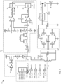
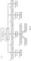
- a transceiver device 15' such as may be used with the wireless power transmission system 10 of FIG. 1 , that incorporates a Q-factor sensor 30 and an excitation circuit 21 described herein.
- the transceiver device 15' includes a controlled switching bridge circuit (operable as either a bridge rectifier or a DC-AC inverter) 16 coupled to a transceiver coil Lxcvr at nodes Ac1 and Ac2, with the capacitor Cxcvr representing the tuning capacitor to align the impedance matching, and the capacitor Cpar representing the parasitic capacitance purposefully added between nodes Ac1 and Ac2 to tune the impedance of the system
- the controlled switching bridge circuit 16 is comprised of transistors T1-T4 controlled by gate voltages G1-G4.
- the transistor T1 has a drain coupled to node Nin, a source coupled to node Ac1, and a gate coupled to gate voltage G1
- the transistor T3 has a drain coupled to node Ac1, a source coupled to node N (which may be ground or another reference voltage), and a gate coupled to gate voltage G3
- the transistor T2 has a drain coupled to node Nin, a source coupled to node Ac2, and a gate coupled to gate voltage G2
- the transistor T4 has a drain coupled to node Ac2, a source coupled to node N, and a gate coupled to gate voltage G4.
- a tank capacitor Ctank is coupled between node Nin and ground.
- a voltage regulator 17 has an input coupled to node Nin and an output coupled to node Nout.
- a battery 18 is selectively coupled between node Nout and ground by a switch SW1, and is selectively coupled between node Nin and node Nout by a switch SW2.
- switch SW1 and SW2 operate out of phase with one another; switch SW1 is closed while switch SW2 is opened when the transceiver device 15' operates as a receiver in a power reception mode with the circuit 16 functioning as an AC-DC rectifier and the regulator functioning to generate the regulated voltage Vreg for charging the battery 18, and switch SW1 is opened while switch SW2 is closed when the device 15' operates as a transmitter in a power transmission mode with the circuit 16 functioning as a DC-AC inverter powered by the battery 18.
- a controller 19' generates the gate voltages G1-G4 for controlling the bridge 16 to operate in the desired rectifier/inverter mode.
- the controller 19' includes a logic core 23 generating control signals Gate_G1, Gate_G2, Gate_G3, and Gate_G4, as well as the Q-factor measurement enable signal Q_en, which is inverted to produce signal Q_En_B.
- a first AND gate 31 performs a logical-AND operation on the signals Gate_G1 and Q_En_B to produce the gate voltage G1.
- a second AND gate 32 performs a logical-AND operation on signals Gate_G2 and Q_En_B to produce the gate voltage G2.
- An OR gate 33 performs a logical-OR on signals Gate_G3 and Q_E to produce the gate voltage G3.
- An OR gate 34 performs a logical-OR on signals Gate_G4 and Q_En to produce the gate voltage G4.
- the controlled switching bridge circuit 16 rectifies the AC current to produce a DC current that charges the tank capacitor Ctank connected to the node Nin, and a rectified voltage Vrect is formed across the tank capacitor Ctank.
- the voltage regulator 17 produces a regulated output voltage Vreg at its output node Nout, which is provided to the battery 18 to thereby charge the battery 18.
- the transceiver device 15' When the transceiver device 15' operates as a transmitter, the voltage of the battery 18 is applied to the node Nin by switch SW2 and becomes the voltage Vrect. Then, the gate voltages G1-G4 are driven by the controller 19 so as to generate a time-varying current flowing through the transceiver coil Lxcvr. Details of this control scheme may be found in United States Application for Patent No. 16/669,068, filed October 30, 2019 .
- An excitation circuit 21 is coupled to the transceiver coil Lxcvr at node Ac1.
- the excitation circuit 21 is comprised of a p-channel transistor MP1 having a source coupled to a supply voltage Vdd, a drain coupled to a first terminal of resistor Re, and a gate coupled to a pad Qe to receive the signal Vin_exc as driven by a driver 22.
- the excitation circuit 21 also includes a diode D1 having an anode coupled to a second terminal of the resistor Re and a cathode coupled to the transceiver coil Lxcvr at node Ac1. Note here that the excitation circuit 21 is off-chip, as well as is the capacitor Cq described below, compared to the other components of the transceiver device 15'.
- a Q-factor sensing circuit 30 includes a capacitor Cq coupled between the cathode of diode D and a pad Qs.
- An n-channel transistor MN1 has a drain coupled to the pad Qs, a source coupled to the source of an n-channel transistor MN2, and a gate coupled to the Q-factor measurement enable signal Q_en.
- the transistor MN2 has its source coupled to the source of the transistor MN1, its drain coupled to a tap node N1 between resistors R1 and R2 (which are series coupled between Vdd and ground), and its gate coupled to receive the Q-factor measurement enable signal Q_En.
- An amplifier 26 has an inverting input terminal coupled to node N1 through a capacitor Cg and has the inverting input terminal further coupled to an output of the amplifier through a capacitor Cf and further has an inverting terminal coupled to receive a common mode voltage Vcm.
- the capacitors Cg and Cf may be adjustable in some cases, allowing for adjustment of the gain of the amplifier 26.
- An output voltage Vout is produced at the output of the amplifier 26. This output voltage Vout is applied to the input of an analog to digital converter (ADC) 24 which converts the analog output voltage to a digital signal ADCout.
- ADC analog to digital converter
- the Q-factor sensing circuit 30 also includes a comparator 27 having a non-inverting input terminal coupled to node N1, an inverting input terminal coupled to a tap node N2 between resistors R3 and R4 coupled in series between the supply voltage Vdd and ground as a voltage divider circuit to produce the common mode voltage Vcm at node N2, and an output at which a comparison output signal Comp_Out is generated.
- a finite state machine (FSM) 25 has inputs at which the comparison output signal Comp_Out and the digital signal ADCout are received, and outputs a control signal Ctrl to the ADC 24 as well as the Vin_exc signal. Note that since the capacitance of the capacitors Cg and Cf may be adjustable, permitting programming of the gain of the amplifier 26, the resolution of the samples produced by the ADC 24 may be adjusted as a result.
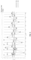
- the comparator 27 has rising and falling threshold values dynamically set by hysteresis dependent upon whether the voltage at its input are rising or falling.
- the comparator has both the comparator rising threshold Vtr and comparator falling threshold Vtl set to Vcm, but with the hysteresis maintained making the actual threshold voltages Vtr and Vtl dynamic, as shown in the graph of the voltage at pad Qs (which will be VLC) in FIG. 5 .
- the comparator 27 permits accurate zero cross (Vcm cross) detection, without compromising the ability of the comparator 27 to utilize hysteresis to reject noise during that zero cross detection.
- the second device 15' may be operated in either transceiver mode (Rx or Tx) or Q-factor measurement mode.
- the controller 19 During transceiver mode, the controller 19 generates the control signals G1-G4 so as to cause the circuit 16 to act as either a receiver or inverter, as described above. Additionally, during transceiver mode, the Q-factor measurement enable signal Q_en is deasserted, turning off transistors MN1 and MN2 to effectively isolate node Qs from Vcm while the diode D effectively blocks the transceiver signal from the circuit 21, and the switching action of the circuit 16 results in the voltage VLC across the coil Lxcvr switching between positive and negative maximum magnitudes, such as -50V and 50V.
- the Q-factor measurement enable signal Q_en is asserted by the controller 19 to turn on transistors MN1 and MN2 to thereby establish a connection from the Qs pad to the center tap of the series connected resistors R1 and R2.
- the transistors T3 and T4 are simultaneously turned on by the controller 19 asserting the gate voltages G3 and G4, thereby shorting the nodes Ac1 and Ac2 to ground.
- the driver 22 drives the p-channel transistor MP1 through pad Qe with a pulse wave Vin_exc during an excitation period to produce an excitation signal, with the duty cycle, frequency, and number of cycles of the pulse wave Vin_exc being set by the firmware of the FSM 25.
- a graph of Vin_exc at pad Qe during the excitation period can be seen in FIG. 6 .
- Vin_exc is low during the excitation period, turning on the p-channel transistor MP1, the coil Lp sinks power from VDD; conversely, when Vin_exc is high turning the excitation period, the p-channel transistor MP1 is turned off.
- the coil Lp is excited with a frequency and duty cycle set by Vin_exc.
- the pulse width and frequency of the excitation signal sets the excitation amplitude of the coil Lp.
- the excitation period continues until the coil Lxcvr reaches a steady state.
- the sensing circuit 30 is protected during the excitation phase by the diode D, resistor Re, and p-channel transistor MP1 having a voltage rating sufficient to withstand the voltage VLC at node Nf.
- the response of the voltage VLC at node Qs (which will be a decaying sine wave oscillating about a common mode voltage Vcm set at the tap between the resistors R1 and R2, as shown in FIG. 6 ) is sensed by the sensing circuitry 23 through the capacitor Cq during a sensing period.
- the comparator 27 asserts the Comp_Out signal when the voltage VLC undergoes a rising zero-cross (meaning that VLC rises above the Vtr threshold, with “zero” here being Vcm as modified by hysteresis, explained above), and deasserts the Comp_Out signal when the voltage VLC undergoes a falling zero-cross (meaning that VLC falls below the Vtl threshold, with “zero” being Vcm as modified by hysteresis as explained above).
- the FSM 25 stores the value of amplitude A1 and continues to compare the value of amplitude A1 to the current value of amplitude AN.
- the FSM 25 saves that value of amplitude AN, thereby reducing the number of values of amplitude AN stored for calculating the Q-factor, and reducing the size of a lookup table used for the natural logarithm function.
- amplitude A1 is measured not only at the peak but also if amplitude A1 is measured at any point that is the time delay period td away from a zero crossing on the curve within the first oscillation cycle during the sensing period.
- the peak and valley of the oscillation cycle may be utilized.
- the FSM 25 stores the value of A1a-A1b and continues to compare the value of A1a-A1b to the current value of ANa-ANb.
- the FSM 25 saves those values of amplitude ANa and amplitude ANb, thereby reducing the number of values of ANa-ANb stored for calculating the Q-factor, and reducing the size of a lookup table used for the natural algorithm function.
- This technique begins with a calibration. During the calibration, it is known that the first device 11 and the foreign object are not in proximity to the second device 15', and the second device 15' is set in Q-factor measurement mode. Then, the excitation period as described above occurs (e.g., the second device 15' is excited without the presence of the second device 11), and its output voltage Vout is sampled during the sensing period. From the samples of Vout, the frequency of Vout during the sensing period, which is the resonance frequency of the second device 15', is determined, and saved as Fr_tx, completing the step of Block 51.
- the operation of the second device 15' and its FSM 25 for performing foreign object detection is described. Beginning with the step at Block 52, when it is not known whether the first device 11 and/or the foreign object are in proximity to the second device 15', the Q-factor measurement mode is engaged, the excitation period as described above occurs, and the output voltage Vout is sampled during the sensing period. From the samples of Vout, the frequency of Vout during the sensing period, which is the resonance frequency of the system (second device 15', first device 11 if present, and foreign object if present), is determined by the FSM 25 and saved as Fr_sys. The first sample of Vout, amplitude A1 is also saved by the FSM 25, as is the amplitude AN sample used together with the amplitude A1 sample to determine the Q-factor, completing the step of Block 52.
- Fr_tx less a margin Fr_margin is greater than Fr_sys at the step of Block 53, then it can be inferred by the FSM 25 that the first device 11 is present but a foreign object is not present at the step of Block 54, so the second device 15' can proceed with transmitting full power wirelessly at the step of Block 55, and this is effectuated by the FSM 25 instructing the logic core 23 accordingly.
- the margin Fr_margin this is a set tolerance threshold either estimated or profiled.
- Fr_sys is less than Fr_tx plus Fr_margin, but greater than Fr_tx-Fr_margin at the step of Block 56, then it can be inferred by the FSM 25 that both the first device 11 and a foreign object are present at the step of Block 57. So as to provide for enhanced accuracy at this step, here, the Q-factor calculated during the Q-factor measurement mode (shown here as Qsys) is compared a Q-factor margin value (shown here as Qmargin) and the amplitude A1 or AN samples are compared to an amplitude margin value (shown here as Amargin).
- Fr_sys is equal to Fr_tx at the step of Block 64, then it can be inferred by the FSM 25 that neither the first device 11 nor a foreign object are present, so periodic pinging can be performed (e.g., every few seconds to check for presence of the first device 11) at the step of Block 65, and the FSM 25 instructs the logic core 23 accordingly.
- sufficiently non-conductive objects such as a plastic case for a smartphone, may have no appreciable effect on the output voltage Vout.
- the comparator 27 utilized by the transceiver device 15' has rising and falling threshold values dynamically set by hysteresis dependent upon whether the voltage at its inputs are rising or falling.
- the comparator has both the comparator rising threshold Vtr and comparator falling threshold Vtl set to Vcm, but with the hysteresis maintained making the actual threshold voltages Vtr and Vtl dynamic.
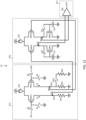
- the advantages provided by this comparator 27 are perhaps best first described with reference to a more generic example of an electronic device 90 including transmitter hardware 91 and receiver or transceiver hardware 92, shown in FIG. 10A .
- the transmitter hardware 91 has a transmitter coil Lxmit coupled thereto, with a capacitor Cxmit being a tuning capacitor.
- the receiver hardware 92 includes a receiver coil Lxcvr, with a capacitor Cxcvr being a tuning capacitor.
- a bridge rectifier 99 has a first input node Ac1 coupled to the first terminal of the receiver coil Lxcvr and a second input node Ac2 coupled to the second terminal of the receiver coil Lxcvr.
- the bridge rectifier 99 has an output node Nin coupled to a voltage regulator 97, with a tank capacitor Ctank being coupled between the output node Nin and ground.
- a rectified voltage Vrect forms across the tank capacitor Ctank.
- a voltage regulator 97 receives the rectified voltage Vrect at its input, and outputs a regulated voltage Vreg at its output to a load 98.
- the bridge rectifier 99 is comprised of a first n-channel transistor T1 having a drain coupled to the output node Nin, a source coupled to the input node Ac1, and a gate coupled to receive the high side on signal HS1_ON generated by driver 93 based upon the low side on signal LS2_ON; a second n-channel transistor T2 having a drain coupled to the output node Nin, a source coupled to the input node Ac2, and a gate coupled to receive the high side on signal HS2_ON generated by the driver 95 based upon the low side on signal LS1_ON; a third n-channel transistor T3 having a drain coupled to the input node Ac1, a source coupled to ground, and a gate coupled to receive the low side on signal LS1_ON, generated by a comparator 94 having its inverting terminal coupled to the input node Ac1 and its non-inverting terminal coupled to ground; and a fourth n-channel transistor T4 having a drain coupled to the input node Ac2, a source
- the transmitter 91 drives the transmitter coil Lxmit with a time varying current, resulting in a time varying current being induced in the receiver coil Lxcvr, which is in turn rectified by the rectifier 99.
- Operation of the rectifier 99 is as follows, with additional reference to FIG. 10B .
- the comparator 94 When the voltage at node Ac1 crosses zero and the voltage at node Ac2 goes high, the comparator 94 outputs the LS1_ON signal at a logic high, turning on the transistors T2 and T3. This has the effect of current flowing from the node Ac2 to the output node Nin through the transistor T2, and current flowing from node Ac2 to node Ac1 through the receiver coil Lxcvr, and from ground to node Ac1 through the transistor T3.
- the comparator 96 When the voltage at node Ac2 crosses zero and the voltage at node Ac1 goes high, the comparator 96 outputs the LS2_ON signal at a logic high, turning on the transistors T1 and T4. This has the effect of current flowing from the node Ac1 to the output node Nin through the transistor T1, from the node Ac1 to node Ac2 through the receiver coil Lxcvr, and from ground to the node Ac2 through the transistor T4.
- the comparators 94 and 96 are hysteresis comparators having a rising threshold Vtr at, for example, 0V and falling threshold Vtl at, for example, -80 mV. This response characteristic can be seen in FIG. 10C .
- This lower threshold Vtl is utilized to help ensure that the direction of current flow in the receiver coil Lxcvr has full reversed before the comparator changes state, avoiding incorrect direction which could lead to oscillation of the output of the comparator.
- each comparator 94, 96 is comprised of: a first p-channel transistor MH1 having a source coupled to a tail current source 101, a drain coupled to ground through a transistor Rh1, and a gate forming the first comparator input (shown as IN1); a second p-channel transistor MH2 having a source coupled to the tail current source 101, a drain coupled to ground through a transistor Rh2, and a gate forming the second comparator input (shown as IN2).
- a resistor Rh3 is selectively connected in parallel with resistor Rh2 by a switch SW.
- a gain stage 102 (shown as an amplifier) has inputs coupled to the drains of the p-channel transistors MH1 and MH2 respectively at nodes No1 and No2, and its output OUT forming the output of the comparator 94, 96.
- the switch SW is operated as a function of the output OUT of the comparator 94, 96.
- this comparator design could be used as the comparator 27 in the transceiver device 15' described above, although functionality could be improved if the comparator 27 were to include an auto-zeroing offset cancellation component.
- the auto-zeroing offset cancellation component cannot function with a resistive load, and therefore the auto-zeroing offset cancellation component is to have an active load.
- the comparator 27 is comprised of a hysteresis stage 27a, an auto-zeroing stage 27b, and a gain stage 27c.
- the hysteresis stage 27a is comprised of p-channel transistors MH1 and MH2 having their sources coupled to a current source 101 and their drains respectively coupled to nodes No1 and No2.
- a resistor Rh1 is coupled between node No1 and ground, and a resistor Rh2 is coupled between node No2 and ground.
- the resistors Rh2 and Rh3 may be equal in resistance.
- the gate of the p-channel transistor MH1 is selectively coupled to the input IN1 by switch S1, and switch S1 operates responsive to deassertion of an auto-zeroing signal AZ.
- the gate of the p-channel transistor MH1 is also selectively coupled to ground by the switch S3, responsive to assertion of the auto-zeroing signal.
- the gate of the p-channel transistor MH2 is selectively coupled to the input IN2 by switch S2, and switch S2 operates responsive to deassertion of the auto-zeroing signal AZ.
- the gate of the p-channel transistor MH2 is also selectively coupled to ground by the switch S4, responsive to assertion of the auto-zeroing signal.
- the auto-zeroing stage 27b is comprised of p-channel transistors MH3 and MH4 having their sources coupled to a tail current source 103 and their drains respectively coupled to nodes No3 and No4.
- the gate of p-channel transistor MH3 is coupled to node No1
- the gate of p-channel transistor MH4 is coupled to node No2.
- An n-channel transistor MH5 has its drain coupled to node No3 and its source coupled to ground
- an n-channel transistor MH6 has its drain coupled to node No4 and its source coupled to ground.
- a switch S6 responsive to assertion of the auto-zeroing signal AZ, couples the gate of the n-channel transistor MH5 to the drain of the n-channel transistor MH5, as well as to the top plate of capacitor Ch1, the bottom plate of which is coupled to ground.
- a switch S7 responsive to assertion of the auto-zeroing signal AZ, couples the gate of the n-channel transistor MH6 to the drain of the n-channel transistor MH6, as well as to the top plate of capacitor Ch2, the bottom plate of which is coupled to ground.
- the gain stage 27c is comprised of an amplifier having inputs coupled to nodes No3 and No4, and providing the comparator output OUT.
- the auto-zeroing signal AZ is deasserted, opening the switches S3, S4, S6, and S7. Note that the offset is still stored across capacitors Ch1 and Ch2.
- the deassertion of the auto-zeroing signal also serves to close switches S1 and S2 so as to receive input.
- the output OUT of the comparator is asserted when IN1 is equal to IN2. Note that any imbalance in resistance between resistors Rh1 and Rh2 is compensated by n-channel transistors MH5 and MH6 as biased by the offset that was stored across capacitors Ch1 and Ch2 during auto-zeroing mode.
- Shown in Fig. 13 is a graph of operating characteristics of the comparator 27 with and without the auto-zeroing function.
- the hysteresis sets Vtr to be 0 V, and Vtl to be - 75 mV.
- the offset without auto-zeroing at Vtr can be 15.3 mV and at Vtl can be 13.1; with auto-zeroing, the offset is reduced to 0.3 mV at Vtr and 5.7 mV at Vtl.
Landscapes
- Engineering & Computer Science (AREA)
- Computer Networks & Wireless Communication (AREA)
- Power Engineering (AREA)
- Charge And Discharge Circuits For Batteries Or The Like (AREA)
- Near-Field Transmission Systems (AREA)
- Transmitters (AREA)
Claims (23)
- Circuit d'alimentation sans fil (15') qui peut fonctionner en mode émetteur-récepteur et en mode de mesure du facteur Q, le circuit d'alimentation sans fil comprenant :une bobine (Lxcvr) ayant des première (Nf) et deuxième bornes ;un pont redresseur (16) ayant une première entrée (Ac1) et une deuxième entrée (Ac2) reliées à la première borne et à la deuxième borne de la bobine, respectivement, et ayant une sortie reliée à un nœud de tension redressée ;un circuit d'excitation (21) relié à la première borne (Nf) de la bobine et configuré pour, pendant un mode de mesure du facteur Q, piloter la bobine avec un signal pulsé ;un circuit de protection reliant la première borne de la bobine à un premier nœud (N1) pendant le mode de mesure du facteur Q et découplant la première borne de la bobine du premier nœud pendant le mode émetteur-récepteur ; etcaractérisé en ce qu'il comprendun circuit de détection du facteur Q (30) comprenant :un amplificateur (26) ayant des entrées reliées au premier nœud et une tension de mode commun (Vcm), et générant un signal de sortie ayant une tension de sortie (Vout) ;un comparateur (27) ayant des entrées reliées au premier nœud et à la tension de mode commun, et générant une sortie de comparaison (Comp_Out) indiquant que la tension de mode commun (Vcm) croise une tension à la première borne de la bobine ;un circuit de traitement (25) configuré pour recevoir la sortie de comparaison et générer un signal d'activation (Ctrl) sur cette base ; etun convertisseur analogique-numérique (24) configuré pour, lorsqu'il est activé par le signal d'activation provenant du circuit de traitement, numériser la tension de sortie et fournir la tension de sortie numérisée (ADCout) au circuit de traitement pour une utilisation dans le calcul d'un facteur Q de la bobine.
- Circuit d'alimentation sans fil selon la revendication 1, dans lequel le comparateur (27) est configuré pour avoir un seuil de croissance (Vtr) égal à une tension de mode commun, un seuil de décroissance (Vt1) égal à la tension de mode commun et une hystérésis, de sorte que, lorsque la tension au premier nœud (N1) décroît, un seuil de croissance effectif est égal au seuil de croissance plus l'hystérésis et un seuil de décroissance effectif est égal au seuil de décroissance, et de sorte que, lorsque la tension au premier nœud croît, le seuil de décroissance effectif est égal au seuil de décroissance moins l'hystérésis et le seuil de croissance effectif est égal au seuil de croissance.
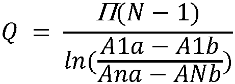
- Circuit d'alimentation sans fil selon la revendication 1 ou 2, dans lequel le circuit de traitement (25) calcule le facteur Q de la bobine sur la base d'une amplitude d'un premier échantillon de la tension de sortie pris à un premier pic de la tension de sortie, et d'une amplitude d'au moins un autre échantillon de la tension de sortie pris à au moins un autre pic de la tension de sortie.
- Circuit d'alimentation sans fil selon la revendication 3, dans lequel le circuit de traitement (25) calcule le facteur Q comme suit :

- Circuit d'alimentation sans fil selon l'une quelconque des revendications 1 à 4, dans lequel le circuit de traitement (25) calcule le facteur Q de la bobine sur la base d'une différence entre un premier échantillon de la tension de sortie pris à un premier pic de la tension de sortie et un deuxième échantillon de la tension de sortie pris à un premier creux de la tension de sortie, et une différence entre un troisième échantillon de la tension de sortie pris à un autre pic de la tension de sortie et un quatrième échantillon de la tension de sortie pris à un autre creux de la tension de sortie.
- Circuit d'alimentation sans fil selon la revendication 5, dans lequel le circuit de traitement (25) calcule le facteur Q comme suit :
- Circuit d'alimentation sans fil selon l'une quelconque des revendications 1 à 6, dans lequel le circuit d'excitation (21) comprend :un pilote (22) configuré pour recevoir un signal de commande et pour générer un signal d'excitation sur la base de celui-ci ; etun transistor à canal p (MP1) ayant une source reliée à une tension d'alimentation (Vdd), un drain relié à une anode d'une diode (D) par l'intermédiaire d'une résistance (Re), et une grille reliée pour recevoir le signal d'excitation ;dans lequel la diode a une cathode reliée à la première borne de la bobine.
- Circuit d'alimentation sans fil selon l'une quelconque des revendications 1 à 7, dans lequel l'amplificateur (26) comporte une borne non inverseuse reliée à la tension de mode commun (Vcm), une borne inverseuse reliée de façon capacitive au premier nœud (N1) par un premier condensateur (Cg), et une sortie reliée à la borne non inverseuse par un deuxième condensateur (Cr), la sortie étant également reliée au convertisseur analogique-numérique (24).
- Circuit d'alimentation sans fil selon l'une quelconque des revendications 1 à 8, dans lequel le comparateur (27) comporte une borne non inverseuse reliée au premier nœud (N1), une borne inverseuse reliée à la tension de mode commun (Vcm) et une sortie au niveau de laquelle la sortie de comparaison est générée.
- Circuit d'alimentation sans fil selon l'une quelconque des revendications 1 à 9, comprenant en outre une première résistance (R1) reliée entre une tension d'alimentation (Vdd) et le premier nœud (N1), et une deuxième résistance (R2) reliée entre le premier nœud et la masse.
- Circuit d'alimentation sans fil selon l'une quelconque des revendications 1 à 10, comprenant en outre une troisième résistance (R3) reliée entre une tension d'alimentation (Vdd) et un deuxième nœud (N2) au niveau duquel la tension de mode commun (Vcm) est produite, et une quatrième résistance (R4) reliée entre le deuxième nœud et la masse.
- Circuit d'alimentation sans fil selon l'une quelconque des revendications 1 à 11, dans lequel le circuit de protection comprend une paire de transistors reliés en série (MN1, MN2) reliés entre la première borne de la bobine et un premier nœud (N1), et ayant leurs grilles reliées à un signal d'activation de détection du facteur Q (Q_En) qui est activé pendant le mode de détection du facteur Q et désactivé sinon.
- Circuit d'alimentation sans fil selon l'une quelconque des revendications 1 à 12,dans lequel, dans le mode de mesure du facteur Q, le circuit de traitement (25) est configuré pour déterminer qu'un deuxième circuit d'alimentation sans fil est à proximité du circuit d'alimentation sans fil mais qu'un objet étranger n'est pas présent entre le deuxième circuit d'alimentation sans fil et le circuit d'alimentation sans fil, en déterminant qu'une fréquence du signal de sortie est inférieure à une fréquence connue du signal de sortie en l'absence du deuxième circuit d'alimentation sans fil et de l'objet étranger moins une valeur de marge ; etcomprenant en outre l'étape consistant à amener le circuit d'alimentation sans fil à transmettre sans fil de l'énergie à un niveau de puissance maximale.
- Circuit d'alimentation sans fil selon l'une quelconque des revendications 1 à 13,dans lequel, dans le mode de mesure du facteur Q, le circuit de traitement (25) est configuré pour déterminer qu'un deuxième circuit d'alimentation sans fil est à proximité du circuit d'alimentation sans fil mais qu'un objet étranger est présent entre le deuxième circuit d'alimentation sans fil et le circuit d'alimentation sans fil, en :déterminant qu'une fréquence du signal de sortie est supérieure à une fréquence connue du signal de sortie en l'absence d'un deuxième circuit d'alimentation sans fil et d'un objet étranger plus une valeur de marge ;déterminant que la fréquence du signal de sortie est inférieure à la fréquence connue du signal de sortie en l'absence du deuxième circuit d'alimentation sans fil et de l'objet étranger moins la valeur de marge ;déterminant si le facteur Q est inférieur à une valeur de marge du facteur Q ;déterminant si un premier échantillon de la tension de sortie est inférieur à une valeur de marge d'amplitude ; etdéterminant si un autre échantillon de la tension de sortie est inférieur à la valeur de marge d'amplitude ;si le facteur Q est inférieur à la valeur de marge du facteur Q, le premier échantillon est inférieur à la valeur de marge d'amplitude et l'autre échantillon est inférieur à la valeur de marge d'amplitude, amenant le circuit d'alimentation sans fil à ne pas transmettre d'énergie sans fil ; etsi le facteur Q n'est pas inférieur à la valeur de marge du facteur Q, ou si le premier échantillon n'est pas inférieur à la valeur de marge d'amplitude, ou si l'autre échantillon n'est pas inférieur à la valeur de marge d'amplitude, amenant le circuit d'alimentation sans fil à transmettre sans fil une quantité limitée d'énergie, la quantité limitée d'énergie étant inférieure à une quantité d'énergie que le circuit d'alimentation sans fil transmettrait autrement.
- Circuit d'alimentation sans fil selon l'une quelconque des revendications 1 à 14, dans lequel, dans le mode de mesure du facteur Q, le circuit de traitement (25) est configuré pour déterminer qu'un deuxième circuit d'alimentation sans fil n'est pas à proximité du circuit d'alimentation sans fil et qu'un objet étranger est à proximité du circuit d'alimentation sans fil, en :déterminant qu'une fréquence du signal de sortie est supérieure à une fréquence connue du signal de sortie en l'absence du deuxième circuit d'alimentation sans fil et de l'objet étranger plus une valeur de marge ; etamenant le circuit d'alimentation sans fil à ne pas transmettre de l'énergie sans fil.
- Circuit d'alimentation sans fil selon l'une quelconque des revendications 1 à 15, dans lequel, dans le mode de mesure du facteur Q, le circuit de traitement (25) est configuré pour déterminer qu'un deuxième circuit d'alimentation sans fil n'est pas à proximité du circuit d'alimentation sans fil et qu'un objet étranger n'est pas non plus à proximité du circuit d'alimentation sans fil, en déterminant qu'une fréquence du signal de sortie est égale à une fréquence connue du signal de sortie en l'absence du deuxième circuit d'alimentation sans fil et de l'objet étranger.
- Procédé de fonctionnement d'un circuit d'alimentation sans fil (15') selon la revendication 1, comprenant les étapes suivantes :1) l'excitation de la bobine (Lxcvr) du circuit d'alimentation sans fil en l'absence d'un deuxième circuit d'alimentation sans fil ;2) la mesure d'une première fréquence de résonance au niveau d'un nœud de détection du circuit d'alimentation sans fil une fois l'excitation libérée ;3) l'excitation de la bobine du circuit d'alimentation sans fil ;4) la mesure d'une deuxième fréquence de résonance au niveau du nœud de détection une fois l'excitation libérée ;5) la détermination d'un facteur Q par le circuit de détection du facteur Q ; et6) sur la base d'au moins la première fréquence de résonance, la deuxième fréquence de résonance et une valeur de marge de fréquence, la détermination de si :a) un deuxième circuit d'alimentation sans fil est à proximité du circuit d'alimentation sans fil mais aucun objet étranger n'est présent entre un deuxième circuit d'alimentation sans fil et le circuit d'alimentation sans fil ;b) un deuxième circuit d'alimentation sans fil est à proximité du circuit d'alimentation sans fil mais un objet étranger est présent entre le deuxième circuit d'alimentation sans fil et le circuit d'alimentation sans fil ;c) un deuxième circuit d'alimentation sans fil n'est pas à proximité du circuit d'alimentation sans fil et un objet étranger est à proximité du circuit d'alimentation sans fil ; oud) un deuxième circuit d'alimentation sans fil n'est pas à proximité du circuit d'alimentation sans fil et un objet étranger n'est pas non plus à proximité du circuit d'alimentation sans fil.
- Procédé selon la revendication 17, dans lequel la détermination que le deuxième circuit d'alimentation sans fil est à proximité du circuit d'alimentation sans fil mais que l'objet étranger n'est pas présent entre le deuxième circuit d'alimentation sans fil et le circuit d'alimentation sans fil est effectuée en déterminant que la deuxième fréquence de résonance est inférieure à la première fréquence de résonance moins la valeur de marge de fréquence ; et comprenant en outre, en réponse à la détermination que le deuxième circuit d'alimentation sans fil est à proximité du circuit d'alimentation sans fil mais que l'objet étranger n'est pas présent entre le deuxième circuit d'alimentation sans fil et le circuit d'alimentation sans fil, l'action consistant à amener le circuit d'alimentation sans fil à transmettre sans fil de l'énergie à un niveau de puissance maximale.
- Procédé selon la revendication 17 ou 18, dans lequel la détermination du facteur Q comprend la prise de premier et deuxième échantillons d'une tension de sortie au niveau du nœud de détection.
- Procédé selon la revendication 19,dans lequel la détermination que le deuxième circuit d'alimentation sans fil est à proximité du circuit d'alimentation sans fil mais que l'objet étranger est présent entre le deuxième circuit d'alimentation sans fil et le circuit d'alimentation sans fil est effectuée en :déterminant que la deuxième fréquence de résonance est supérieure à la première fréquence de résonance plus la valeur de marge de fréquence ;déterminant que la deuxième fréquence de résonance est inférieure à la première fréquence de résonance moins la valeur de marge de fréquence ;déterminant si le facteur Q est inférieur à une valeur de marge du facteur Q ;déterminant si le premier échantillon est inférieur à une valeur de marge d'amplitude ; etdéterminant si le deuxième échantillon est inférieur à la valeur de marge d'amplitude ;comprenant en outre, si le facteur Q est inférieur à la valeur de marge du facteur Q, le premier échantillon est inférieur à la valeur de marge d'amplitude, et le deuxième échantillon est inférieur à la valeur de marge d'amplitude, l'action consistant à amener le circuit d'alimentation sans fil à ne pas transmettre d'énergie sans fil ; etcomprenant en outre, si le facteur Q n'est pas inférieur à la valeur de marge du facteur Q, ou si le premier échantillon n'est pas inférieur à la valeur de marge d'amplitude, ou si le deuxième échantillon n'est pas inférieur à la valeur de marge d'amplitude, l'action consistant à amener le circuit d'alimentation sans fil à transmettre sans fil une quantité limitée d'énergie, la quantité limitée d'énergie étant inférieure à une quantité d'énergie que le circuit d'alimentation sans fil transmettrait sinon.
- Procédé selon l'une quelconque des revendications 17 à 20, dans lequel la détermination que le deuxième circuit d'alimentation sans fil n'est pas à proximité du circuit d'alimentation sans fil et que l'objet étranger est à proximité du circuit d'alimentation sans fil est effectuée en déterminant que la deuxième fréquence de résonance est supérieure à la première fréquence de résonance plus la valeur de marge de fréquence ; et comprenant en outre, en réponse à la détermination que le deuxième circuit d'alimentation sans fil n'est pas à proximité du circuit d'alimentation sans fil et que l'objet étranger est à proximité du circuit d'alimentation sans fil, l'action consistant à amener le circuit d'alimentation sans fil à ne pas transmettre d'énergie sans fil.
- Procédé selon l'une quelconque des revendications 17 à 21, dans lequel la détermination que le deuxième circuit d'alimentation sans fil n'est pas à proximité du circuit d'alimentation sans fil et que l'objet étranger n'est pas non plus à proximité du circuit d'alimentation sans fil est effectuée en déterminant que la deuxième fréquence de résonance est égale à la première fréquence de résonance.
- Procédé selon l'une quelconque des revendications 17 à 22, de fonctionnement du circuit d'alimentation sans fil selon l'une quelconque des revendications 1 à 16.
Applications Claiming Priority (1)
| Application Number | Priority Date | Filing Date | Title |
|---|---|---|---|
| US17/037,982 US11152822B1 (en) | 2020-09-30 | 2020-09-30 | Foreign objection detection sensing circuit for wireless power transmission systems |
Publications (3)
| Publication Number | Publication Date |
|---|---|
| EP3989397A2 EP3989397A2 (fr) | 2022-04-27 |
| EP3989397A3 EP3989397A3 (fr) | 2022-06-29 |
| EP3989397B1 true EP3989397B1 (fr) | 2025-04-30 |
Family
ID=77897530
Family Applications (1)
| Application Number | Title | Priority Date | Filing Date |
|---|---|---|---|
| EP21198160.0A Active EP3989397B1 (fr) | 2020-09-30 | 2021-09-22 | Circuit de détection d'objets étrangers pour systèmes de transmission de puissance sans fil |
Country Status (3)
| Country | Link |
|---|---|
| US (2) | US11152822B1 (fr) |
| EP (1) | EP3989397B1 (fr) |
| CN (1) | CN114336997A (fr) |
Families Citing this family (2)
| Publication number | Priority date | Publication date | Assignee | Title |
|---|---|---|---|---|
| CN115098419B (zh) * | 2022-06-17 | 2023-04-07 | 锐宸微(上海)科技有限公司 | 具有过电压保护的电压模式发射器电路 |
| FR3156535B1 (fr) * | 2023-12-07 | 2025-11-21 | Commissariat Energie Atomique | Mesure de la phase d’une impédance complexe par seuillage |
Family Cites Families (21)
| Publication number | Priority date | Publication date | Assignee | Title |
|---|---|---|---|---|
| US5132889A (en) * | 1991-05-15 | 1992-07-21 | Ibm Corporation | Resonant-transition DC-to-DC converter |
| US7042199B1 (en) * | 2003-07-28 | 2006-05-09 | The United States Of America As Represented By The Administrator Of The National Aeronautics And Space Administration | Series connected buck-boost regulator |
| US7304866B2 (en) * | 2004-02-10 | 2007-12-04 | O2Micro International Limited | System and method for power converter switch control |
| JP5665571B2 (ja) * | 2011-01-28 | 2015-02-04 | ルネサスエレクトロニクス株式会社 | 半導体集積回路およびその動作方法 |
| US8861164B2 (en) | 2011-02-04 | 2014-10-14 | Fairchild Semiconductor Corporation | Integrated overdrive and overvoltage protection device |
| US20120223591A1 (en) | 2011-03-02 | 2012-09-06 | Electronics And Telecommunications Research Institute | Overvoltage protection circuit, power transmission device including the same, and control method thereof |
| KR101786945B1 (ko) | 2011-07-22 | 2017-10-19 | 한국전자통신연구원 | 전력 송신 장치 및 전력 수신 장치 |
| JP5840886B2 (ja) * | 2011-07-25 | 2016-01-06 | ソニー株式会社 | 検知装置、受電装置、送電装置、非接触電力伝送システム及び検知方法 |
| US9001529B2 (en) * | 2012-01-17 | 2015-04-07 | Texas Instruments Incorporated | System and method for power transfer control based on available input power |
| JP5915904B2 (ja) | 2012-06-22 | 2016-05-11 | ソニー株式会社 | 処理装置、処理方法、及び、プログラム |
| US9726518B2 (en) | 2012-07-13 | 2017-08-08 | Qualcomm Incorporated | Systems, methods, and apparatus for detection of metal objects in a predetermined space |
| AT515242B1 (de) * | 2013-12-20 | 2020-04-15 | Fronius Int Gmbh | Verfahren zum Steuern eines Vollbrücken DC/DC-Wandlers |
| US9939539B2 (en) | 2014-04-04 | 2018-04-10 | Texas Instruments Incorporated | Wireless power receiver and/or foreign object detection by a wireless power transmitter |
| US10199881B2 (en) * | 2015-10-23 | 2019-02-05 | Mediatek Inc. | Robust foreign objects detection |
| CN107204699B (zh) | 2016-03-15 | 2021-05-07 | 恩智浦美国有限公司 | 谐振储能网络的q因子的确定 |
| SG10201708902RA (en) | 2017-02-02 | 2018-09-27 | Apple Inc | Wireless Charging System With Object Detection |
| WO2019203420A1 (fr) | 2018-04-18 | 2019-10-24 | 엘지전자 주식회사 | Appareil et procédé permettant de détecter un corps étranger dans un système de transmission d'énergie sans fil |
| TWI742404B (zh) | 2018-07-19 | 2021-10-11 | 新加坡商聯發科技(新加坡)私人有限公司 | 無線功率傳輸系統之異物偵測技術 |
| CN111245107B (zh) * | 2018-11-28 | 2024-03-19 | 集成装置技术公司 | 无线电力传送系统中利用线圈电流感测的增强型异物检测 |
| CN111313569A (zh) * | 2018-12-11 | 2020-06-19 | 恩智浦美国有限公司 | 无线充电系统中的异物检测电路的q因子确定 |
| CN111208357B (zh) | 2020-02-17 | 2020-12-08 | 珠海智融科技有限公司 | Q值检测电路和q值检测电路的工作方法 |
-
2020
- 2020-09-30 US US17/037,982 patent/US11152822B1/en active Active
-
2021
- 2021-08-23 US US17/408,824 patent/US11658518B2/en active Active
- 2021-09-22 EP EP21198160.0A patent/EP3989397B1/fr active Active
- 2021-09-29 CN CN202111151882.8A patent/CN114336997A/zh active Pending
Also Published As
| Publication number | Publication date |
|---|---|
| US11658518B2 (en) | 2023-05-23 |
| CN114336997A (zh) | 2022-04-12 |
| EP3989397A3 (fr) | 2022-06-29 |
| US20220103019A1 (en) | 2022-03-31 |
| EP3989397A2 (fr) | 2022-04-27 |
| US11152822B1 (en) | 2021-10-19 |
Similar Documents
| Publication | Publication Date | Title |
|---|---|---|
| EP4092862B1 (fr) | Circuit de charge sans fil, procédé de charge sans fil, dispositif et système | |
| CN106300445B (zh) | 电力输送装置以及电力接收装置及包含其的电子设备 | |
| US10601264B2 (en) | Methods for detecting and identifying a receiver in an inductive power transfer system | |
| US7847438B2 (en) | Power transmission device, electronic instrument, and waveform monitoring circuit | |
| EP3989397B1 (fr) | Circuit de détection d'objets étrangers pour systèmes de transmission de puissance sans fil | |
| TWI542112B (zh) | 電子設備的無線充電方法及相關裝置 | |
| US20160146877A1 (en) | Load Connection Detection | |
| CN103080776B (zh) | 测量设备尤其用于检测金属物体的测量设备 | |
| US9190862B2 (en) | Charging current calibration | |
| US10819129B2 (en) | Battery charging system including battery gauge | |
| US6982559B2 (en) | Accurate and efficient sensing circuit and method for bi-directional signals | |
| CN104201892A (zh) | 一种隔离反激式高频开关电源的输入电压检测方法及电路 | |
| CN112271764B (zh) | 一种过流检测电路及电池保护装置 | |
| US11588353B2 (en) | Quality factor estimation of an inductive element | |
| CN110829609B (zh) | 无线充电发射装置及其集成电路装置 | |
| US11804732B2 (en) | Wireless power transmission device, and transmission power control method therefor | |
| US12519347B2 (en) | Foreign object detection by frequency bandwidth comparison | |
| US20130093429A1 (en) | Battery gauge estimation device | |
| JP6736704B2 (ja) | 受信機を検出する方法及び誘導電力伝送システム | |
| US20150042349A1 (en) | Voltage measurement | |
| WO2025053872A1 (fr) | Détection d'objet étranger par comparaison de largeur de bande de fréquence | |
| CN121308377A (zh) | 无线电能传输系统的互感和负载电压识别电路及识别方法 |
Legal Events
| Date | Code | Title | Description |
|---|---|---|---|
| PUAI | Public reference made under article 153(3) epc to a published international application that has entered the european phase |
Free format text: ORIGINAL CODE: 0009012 |
|
| STAA | Information on the status of an ep patent application or granted ep patent |
Free format text: STATUS: REQUEST FOR EXAMINATION WAS MADE |
|
| 17P | Request for examination filed |
Effective date: 20210922 |
|
| AK | Designated contracting states |
Kind code of ref document: A2 Designated state(s): AL AT BE BG CH CY CZ DE DK EE ES FI FR GB GR HR HU IE IS IT LI LT LU LV MC MK MT NL NO PL PT RO RS SE SI SK SM TR |
|
| PUAL | Search report despatched |
Free format text: ORIGINAL CODE: 0009013 |
|
| AK | Designated contracting states |
Kind code of ref document: A3 Designated state(s): AL AT BE BG CH CY CZ DE DK EE ES FI FR GB GR HR HU IE IS IT LI LT LU LV MC MK MT NL NO PL PT RO RS SE SI SK SM TR |
|
| RIC1 | Information provided on ipc code assigned before grant |
Ipc: H02J 50/12 20160101ALI20220525BHEP Ipc: H02J 50/60 20160101AFI20220525BHEP |
|
| GRAP | Despatch of communication of intention to grant a patent |
Free format text: ORIGINAL CODE: EPIDOSNIGR1 |
|
| STAA | Information on the status of an ep patent application or granted ep patent |
Free format text: STATUS: GRANT OF PATENT IS INTENDED |
|
| INTG | Intention to grant announced |
Effective date: 20241219 |
|
| GRAS | Grant fee paid |
Free format text: ORIGINAL CODE: EPIDOSNIGR3 |
|
| GRAA | (expected) grant |
Free format text: ORIGINAL CODE: 0009210 |
|
| STAA | Information on the status of an ep patent application or granted ep patent |
Free format text: STATUS: THE PATENT HAS BEEN GRANTED |
|
| AK | Designated contracting states |
Kind code of ref document: B1 Designated state(s): AL AT BE BG CH CY CZ DE DK EE ES FI FR GB GR HR HU IE IS IT LI LT LU LV MC MK MT NL NO PL PT RO RS SE SI SK SM TR |
|
| REG | Reference to a national code |
Ref country code: CH Ref legal event code: EP Ref country code: GB Ref legal event code: FG4D |
|
| REG | Reference to a national code |
Ref country code: DE Ref legal event code: R096 Ref document number: 602021029914 Country of ref document: DE |
|
| REG | Reference to a national code |
Ref country code: IE Ref legal event code: FG4D |
|
| REG | Reference to a national code |
Ref country code: NL Ref legal event code: MP Effective date: 20250430 |
|
| REG | Reference to a national code |
Ref country code: AT Ref legal event code: MK05 Ref document number: 1791017 Country of ref document: AT Kind code of ref document: T Effective date: 20250430 |
|
| PG25 | Lapsed in a contracting state [announced via postgrant information from national office to epo] |
Ref country code: PT Free format text: LAPSE BECAUSE OF FAILURE TO SUBMIT A TRANSLATION OF THE DESCRIPTION OR TO PAY THE FEE WITHIN THE PRESCRIBED TIME-LIMIT Effective date: 20250901 Ref country code: ES Free format text: LAPSE BECAUSE OF FAILURE TO SUBMIT A TRANSLATION OF THE DESCRIPTION OR TO PAY THE FEE WITHIN THE PRESCRIBED TIME-LIMIT Effective date: 20250430 Ref country code: FI Free format text: LAPSE BECAUSE OF FAILURE TO SUBMIT A TRANSLATION OF THE DESCRIPTION OR TO PAY THE FEE WITHIN THE PRESCRIBED TIME-LIMIT Effective date: 20250430 |
|
| PGFP | Annual fee paid to national office [announced via postgrant information from national office to epo] |
Ref country code: DE Payment date: 20250820 Year of fee payment: 5 |
|
| REG | Reference to a national code |
Ref country code: LT Ref legal event code: MG9D |
|
| PG25 | Lapsed in a contracting state [announced via postgrant information from national office to epo] |
Ref country code: NO Free format text: LAPSE BECAUSE OF FAILURE TO SUBMIT A TRANSLATION OF THE DESCRIPTION OR TO PAY THE FEE WITHIN THE PRESCRIBED TIME-LIMIT Effective date: 20250730 Ref country code: GR Free format text: LAPSE BECAUSE OF FAILURE TO SUBMIT A TRANSLATION OF THE DESCRIPTION OR TO PAY THE FEE WITHIN THE PRESCRIBED TIME-LIMIT Effective date: 20250731 |
|
| PG25 | Lapsed in a contracting state [announced via postgrant information from national office to epo] |
Ref country code: NL Free format text: LAPSE BECAUSE OF FAILURE TO SUBMIT A TRANSLATION OF THE DESCRIPTION OR TO PAY THE FEE WITHIN THE PRESCRIBED TIME-LIMIT Effective date: 20250430 Ref country code: PL Free format text: LAPSE BECAUSE OF FAILURE TO SUBMIT A TRANSLATION OF THE DESCRIPTION OR TO PAY THE FEE WITHIN THE PRESCRIBED TIME-LIMIT Effective date: 20250430 |
|
| PG25 | Lapsed in a contracting state [announced via postgrant information from national office to epo] |
Ref country code: BG Free format text: LAPSE BECAUSE OF FAILURE TO SUBMIT A TRANSLATION OF THE DESCRIPTION OR TO PAY THE FEE WITHIN THE PRESCRIBED TIME-LIMIT Effective date: 20250430 |
|
| PG25 | Lapsed in a contracting state [announced via postgrant information from national office to epo] |
Ref country code: HR Free format text: LAPSE BECAUSE OF FAILURE TO SUBMIT A TRANSLATION OF THE DESCRIPTION OR TO PAY THE FEE WITHIN THE PRESCRIBED TIME-LIMIT Effective date: 20250430 |
|
| PG25 | Lapsed in a contracting state [announced via postgrant information from national office to epo] |
Ref country code: AT Free format text: LAPSE BECAUSE OF FAILURE TO SUBMIT A TRANSLATION OF THE DESCRIPTION OR TO PAY THE FEE WITHIN THE PRESCRIBED TIME-LIMIT Effective date: 20250430 |
|
| PG25 | Lapsed in a contracting state [announced via postgrant information from national office to epo] |
Ref country code: RS Free format text: LAPSE BECAUSE OF FAILURE TO SUBMIT A TRANSLATION OF THE DESCRIPTION OR TO PAY THE FEE WITHIN THE PRESCRIBED TIME-LIMIT Effective date: 20250731 |
|
| PG25 | Lapsed in a contracting state [announced via postgrant information from national office to epo] |
Ref country code: IS Free format text: LAPSE BECAUSE OF FAILURE TO SUBMIT A TRANSLATION OF THE DESCRIPTION OR TO PAY THE FEE WITHIN THE PRESCRIBED TIME-LIMIT Effective date: 20250830 |
|
| PG25 | Lapsed in a contracting state [announced via postgrant information from national office to epo] |
Ref country code: LV Free format text: LAPSE BECAUSE OF FAILURE TO SUBMIT A TRANSLATION OF THE DESCRIPTION OR TO PAY THE FEE WITHIN THE PRESCRIBED TIME-LIMIT Effective date: 20250430 |
|
| PG25 | Lapsed in a contracting state [announced via postgrant information from national office to epo] |
Ref country code: DK Free format text: LAPSE BECAUSE OF FAILURE TO SUBMIT A TRANSLATION OF THE DESCRIPTION OR TO PAY THE FEE WITHIN THE PRESCRIBED TIME-LIMIT Effective date: 20250430 Ref country code: SM Free format text: LAPSE BECAUSE OF FAILURE TO SUBMIT A TRANSLATION OF THE DESCRIPTION OR TO PAY THE FEE WITHIN THE PRESCRIBED TIME-LIMIT Effective date: 20250430 |
|
| PG25 | Lapsed in a contracting state [announced via postgrant information from national office to epo] |
Ref country code: CZ Free format text: LAPSE BECAUSE OF FAILURE TO SUBMIT A TRANSLATION OF THE DESCRIPTION OR TO PAY THE FEE WITHIN THE PRESCRIBED TIME-LIMIT Effective date: 20250430 |
|
| PG25 | Lapsed in a contracting state [announced via postgrant information from national office to epo] |
Ref country code: EE Free format text: LAPSE BECAUSE OF FAILURE TO SUBMIT A TRANSLATION OF THE DESCRIPTION OR TO PAY THE FEE WITHIN THE PRESCRIBED TIME-LIMIT Effective date: 20250430 |
|
| PG25 | Lapsed in a contracting state [announced via postgrant information from national office to epo] |
Ref country code: SK Free format text: LAPSE BECAUSE OF FAILURE TO SUBMIT A TRANSLATION OF THE DESCRIPTION OR TO PAY THE FEE WITHIN THE PRESCRIBED TIME-LIMIT Effective date: 20250430 Ref country code: RO Free format text: LAPSE BECAUSE OF FAILURE TO SUBMIT A TRANSLATION OF THE DESCRIPTION OR TO PAY THE FEE WITHIN THE PRESCRIBED TIME-LIMIT Effective date: 20250430 |
|
| PG25 | Lapsed in a contracting state [announced via postgrant information from national office to epo] |
Ref country code: IT Free format text: LAPSE BECAUSE OF FAILURE TO SUBMIT A TRANSLATION OF THE DESCRIPTION OR TO PAY THE FEE WITHIN THE PRESCRIBED TIME-LIMIT Effective date: 20250430 |