EP3979321A1 - Halbleiterbauelement - Google Patents
Halbleiterbauelement Download PDFInfo
- Publication number
- EP3979321A1 EP3979321A1 EP21197279.9A EP21197279A EP3979321A1 EP 3979321 A1 EP3979321 A1 EP 3979321A1 EP 21197279 A EP21197279 A EP 21197279A EP 3979321 A1 EP3979321 A1 EP 3979321A1
- Authority
- EP
- European Patent Office
- Prior art keywords
- film
- plug
- semiconductor device
- conductive film
- ferroelectric
- Prior art date
- Legal status (The legal status is an assumption and is not a legal conclusion. Google has not performed a legal analysis and makes no representation as to the accuracy of the status listed.)
- Pending
Links
Images










Classifications
-
- H—ELECTRICITY
- H10—SEMICONDUCTOR DEVICES; ELECTRIC SOLID-STATE DEVICES NOT OTHERWISE PROVIDED FOR
- H10D—INORGANIC ELECTRIC SEMICONDUCTOR DEVICES
- H10D64/00—Electrodes of devices having potential barriers
- H10D64/01—Manufacture or treatment
- H10D64/031—Manufacture or treatment of data-storage electrodes
- H10D64/035—Manufacture or treatment of data-storage electrodes comprising conductor-insulator-conductor-insulator-semiconductor structures
-
- H—ELECTRICITY
- H10—SEMICONDUCTOR DEVICES; ELECTRIC SOLID-STATE DEVICES NOT OTHERWISE PROVIDED FOR
- H10B—ELECTRONIC MEMORY DEVICES
- H10B51/00—Ferroelectric RAM [FeRAM] devices comprising ferroelectric memory transistors
- H10B51/30—Ferroelectric RAM [FeRAM] devices comprising ferroelectric memory transistors characterised by the memory core region
-
- G—PHYSICS
- G11—INFORMATION STORAGE
- G11C—STATIC STORES
- G11C11/00—Digital stores characterised by the use of particular electric or magnetic storage elements; Storage elements therefor
- G11C11/21—Digital stores characterised by the use of particular electric or magnetic storage elements; Storage elements therefor using electric elements
- G11C11/22—Digital stores characterised by the use of particular electric or magnetic storage elements; Storage elements therefor using electric elements using ferroelectric elements
- G11C11/221—Digital stores characterised by the use of particular electric or magnetic storage elements; Storage elements therefor using electric elements using ferroelectric elements using ferroelectric capacitors
-
- G—PHYSICS
- G11—INFORMATION STORAGE
- G11C—STATIC STORES
- G11C11/00—Digital stores characterised by the use of particular electric or magnetic storage elements; Storage elements therefor
- G11C11/21—Digital stores characterised by the use of particular electric or magnetic storage elements; Storage elements therefor using electric elements
- G11C11/22—Digital stores characterised by the use of particular electric or magnetic storage elements; Storage elements therefor using electric elements using ferroelectric elements
- G11C11/223—Digital stores characterised by the use of particular electric or magnetic storage elements; Storage elements therefor using electric elements using ferroelectric elements using MOS with ferroelectric gate insulating film
-
- H—ELECTRICITY
- H10—SEMICONDUCTOR DEVICES; ELECTRIC SOLID-STATE DEVICES NOT OTHERWISE PROVIDED FOR
- H10D—INORGANIC ELECTRIC SEMICONDUCTOR DEVICES
- H10D1/00—Resistors, capacitors or inductors
- H10D1/60—Capacitors
- H10D1/68—Capacitors having no potential barriers
-
- H—ELECTRICITY
- H10—SEMICONDUCTOR DEVICES; ELECTRIC SOLID-STATE DEVICES NOT OTHERWISE PROVIDED FOR
- H10D—INORGANIC ELECTRIC SEMICONDUCTOR DEVICES
- H10D64/00—Electrodes of devices having potential barriers
- H10D64/01—Manufacture or treatment
- H10D64/031—Manufacture or treatment of data-storage electrodes
- H10D64/033—Manufacture or treatment of data-storage electrodes comprising ferroelectric layers
-
- H—ELECTRICITY
- H10—SEMICONDUCTOR DEVICES; ELECTRIC SOLID-STATE DEVICES NOT OTHERWISE PROVIDED FOR
- H10D—INORGANIC ELECTRIC SEMICONDUCTOR DEVICES
- H10D64/00—Electrodes of devices having potential barriers
- H10D64/20—Electrodes characterised by their shapes, relative sizes or dispositions
- H10D64/27—Electrodes not carrying the current to be rectified, amplified, oscillated or switched, e.g. gates
- H10D64/311—Gate electrodes for field-effect devices
- H10D64/411—Gate electrodes for field-effect devices for FETs
- H10D64/511—Gate electrodes for field-effect devices for FETs for IGFETs
- H10D64/514—Gate electrodes for field-effect devices for FETs for IGFETs characterised by the insulating layers
-
- H—ELECTRICITY
- H10—SEMICONDUCTOR DEVICES; ELECTRIC SOLID-STATE DEVICES NOT OTHERWISE PROVIDED FOR
- H10D—INORGANIC ELECTRIC SEMICONDUCTOR DEVICES
- H10D64/00—Electrodes of devices having potential barriers
- H10D64/60—Electrodes characterised by their materials
- H10D64/66—Electrodes having a conductor capacitively coupled to a semiconductor by an insulator, e.g. MIS electrodes
- H10D64/68—Electrodes having a conductor capacitively coupled to a semiconductor by an insulator, e.g. MIS electrodes characterised by the insulator, e.g. by the gate insulator
- H10D64/689—Electrodes having a conductor capacitively coupled to a semiconductor by an insulator, e.g. MIS electrodes characterised by the insulator, e.g. by the gate insulator having ferroelectric layers
-
- H—ELECTRICITY
- H10—SEMICONDUCTOR DEVICES; ELECTRIC SOLID-STATE DEVICES NOT OTHERWISE PROVIDED FOR
- H10W—GENERIC PACKAGES, INTERCONNECTIONS, CONNECTORS OR OTHER CONSTRUCTIONAL DETAILS OF DEVICES COVERED BY CLASS H10
- H10W20/00—Interconnections in chips, wafers or substrates
- H10W20/40—Interconnections external to wafers or substrates, e.g. back-end-of-line [BEOL] metallisations or vias connecting to gate electrodes
- H10W20/41—Interconnections external to wafers or substrates, e.g. back-end-of-line [BEOL] metallisations or vias connecting to gate electrodes characterised by their conductive parts
- H10W20/42—Vias, e.g. via plugs
-
- G—PHYSICS
- G11—INFORMATION STORAGE
- G11C—STATIC STORES
- G11C11/00—Digital stores characterised by the use of particular electric or magnetic storage elements; Storage elements therefor
- G11C11/21—Digital stores characterised by the use of particular electric or magnetic storage elements; Storage elements therefor using electric elements
- G11C11/22—Digital stores characterised by the use of particular electric or magnetic storage elements; Storage elements therefor using electric elements using ferroelectric elements
- G11C11/225—Auxiliary circuits
- G11C11/2273—Reading or sensing circuits or methods
-
- G—PHYSICS
- G11—INFORMATION STORAGE
- G11C—STATIC STORES
- G11C11/00—Digital stores characterised by the use of particular electric or magnetic storage elements; Storage elements therefor
- G11C11/21—Digital stores characterised by the use of particular electric or magnetic storage elements; Storage elements therefor using electric elements
- G11C11/22—Digital stores characterised by the use of particular electric or magnetic storage elements; Storage elements therefor using electric elements using ferroelectric elements
- G11C11/225—Auxiliary circuits
- G11C11/2275—Writing or programming circuits or methods
-
- H—ELECTRICITY
- H10—SEMICONDUCTOR DEVICES; ELECTRIC SOLID-STATE DEVICES NOT OTHERWISE PROVIDED FOR
- H10D—INORGANIC ELECTRIC SEMICONDUCTOR DEVICES
- H10D30/00—Field-effect transistors [FET]
- H10D30/01—Manufacture or treatment
- H10D30/021—Manufacture or treatment of FETs having insulated gates [IGFET]
- H10D30/0415—Manufacture or treatment of FETs having insulated gates [IGFET] of FETs having ferroelectric gate insulators
-
- H—ELECTRICITY
- H10—SEMICONDUCTOR DEVICES; ELECTRIC SOLID-STATE DEVICES NOT OTHERWISE PROVIDED FOR
- H10D—INORGANIC ELECTRIC SEMICONDUCTOR DEVICES
- H10D30/00—Field-effect transistors [FET]
- H10D30/60—Insulated-gate field-effect transistors [IGFET]
- H10D30/701—IGFETs having ferroelectric gate insulators, e.g. ferroelectric FETs
Definitions
- the present disclosure relates to a semiconductor device, for example, a semiconductor device having a ferroelectric film.
- Patent Document 1 Japanese Unexamined Patent Application Publication No. 2019-201172
- a ferroelectric memory including a ferroelectric film are known as a storage element operating at low voltages.
- a write state and an erase state are determined in accordance with a polarization direction of the ferroelectric film.
- a semiconductor device described in Patent Document 1 includes a semiconductor substrate, an insulating film formed on the semiconductor substrate, a ferroelectric film formed on the insulating film, a metal film formed on the ferroelectric film, and a gate electrode formed on the metal film.
- the ferroelectric film described in Patent Document 1 is formed by performing heat treatment to a laminated film including a first amorphous film, a plurality of particles formed on the first amorphous film, and a second amorphous film formed on the first amorphous film so as to cover the plurality of particles.
- the plurality of particles functions as nuclei
- a crystal grain size in the ferroelectric film becomes uniform.
- a variation of a threshold voltage of the semiconductor device can be reduced.
- the ferroelectric film and the insulating film is two capacitive components coupled in series with each other. Therefore, a rewrite voltage applied to the gate electrode is distributed respectively to the ferroelectric film and the insulating film. From the viewpoint of increasing the partial voltage of the ferroelectric film, it is preferable to increase a thickness of the ferroelectric film, or to reduce a thickness of the insulating film. However, if the thickness of the insulating film is too small, a reliability of the semiconductor device deteriorates. Thus, the conventional semiconductor device has room to be improved from the viewpoint of enhancing reliability.
- a semiconductor device includes an semiconductor substrate including a source region and a drain region formed on a main surface of the semiconductor substrate; an insulating film formed on the main surface of the semiconductor substrate such that the insulating film is located between the source region and the drain region in a plan view; a first conductive film formed on the insulating film; a ferroelectric film formed on the first conductive film; an insulating layer formed on the semiconductor substrate such that the insulating layer covers the first conductive film and the ferroelectric film; a first plug formed in the insulating layer such that the first plug reaches the first conductive film; and a second plug formed in the insulating layer such that the second plug reaches the ferroelectric film.
- a material of the ferroelectric film contains hafnium and oxygen. In plan view, a size of the ferroelectric film is smaller than a size of the insulating film.
- the reliability of the semiconductor device is enhanced.
- FIG. 1 is a plan view illustrating an exemplary configuration of a main portion of a semiconductor device SD according to present embodiment.
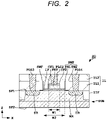
- FIG. 2 is a cross-sectional view illustrating an exemplary configuration of the main portion of the semiconductor device SD according to the present embodiment.
- FIG. 2 is the cross-sectional view taken along line A-A of FIG. 1 .
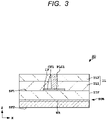
- FIG. 3 is a cross-sectional view illustrating an exemplary configuration of the main portion of the semiconductor device SD according to the present embodiment.
- FIG. 3 is the cross-sectional view taken along line B-B of FIG. 1 .
- the semiconductor device SD includes a semiconductor substrate SUB, an isolation insulating film IIF, an insulating film IF, a first conductive film CF1, a ferroelectric film FEF, a second conductive film CF2, a pair of sidewall insulating films SWF, an insulating layer IL, a first plug PLG1, a second plug PLG2, a third plug PLG3 and a fourth plug PLG4.
- the insulating layer IL is omitted from the viewpoint of visibility.
- the X-direction is an opposing direction in which a source region SR and a drain region DR are opposite to each other.
- the X-direction is along a main surface of the semiconductor substrate SUB (a first surface SF1).
- Y-direction, in plan view is a direction along a long side of the ferroelectric film FEF.
- the Y-direction, in plan view is a direction perpendicular to the X direction.
- Z-direction is a thickness direction of the ferroelectric film FEF.
- X-direction, Y-direction and Z-direction are perpendicular to each other.
- the semiconductor substrate SUB has a first surface (main surface) SF1, and a second surface SF2 opposite to the first surface SF1.
- the first surface SF1 of the semiconductor substrate SUB a semiconductor element such as a transistor, a resistor and a capacitor may be formed.
- a ferroelectric memory cell is formed on the first surface SF1 of the semiconductor substrate SUB.
- a Type of the semiconductor substrate SUB is, for example, a silicon-single-crystal substrate. Resistivity of the semiconductor substrate SUB, for example, 1 ⁇ cm or more and 10 ⁇ cm or less.
- the first surface SF1 of the semiconductor substrate SUB, a well region WR, the source region SR, the drain region DR and the isolation insulating film IIF are formed.
- the well region WR, the source region SR and the drain region DR constitute a portion of the ferroelectric memory cell.
- the well region WR directly contacts with the source region SR and the drain region DR.
- the well region WR is formed between the source region SR and the drain region DR.
- the well region WR contains an impurity of a predetermined concentration.
- the source region SR and the drain region DR are spaced apart from each other.
- Each of the source region SR and the drain region DR contains an impurity of a predetermined concentration.
- a silicide layer may be formed on an upper surface of each of the source region SR and the drain region DR.
- a material of the silicide layer is, for example, cobalt silicide, nickel silicide, platinum silicide, or nickel platinum silicide.
- the isolation insulating film IIF in plan view, surrounds a region which functions as the ferroelectric memory cell.
- the isolation insulating film IIF in plan view, is formed such that isolation insulating film IIF surrounds a region sandwiched between the source region SR and the drain region DR (a part of the well region WR), the source region SR, and the drain region SR.
- the isolated insulating film IIF is formed on the first surface SF1 of the semiconductor substrate SUB.
- a material of the isolation insulating film IIF is, for example, silicon oxide.
- the insulating film IF suppresses from introducing unintentional electrons into the ferroelectric film FEF from the semiconductor substrate SUB during operation of the semiconductor device SD.
- the insulating film IF is formed on the first surface SF1 of the semiconductor substrate SUB.
- the insulating film IF is formed such that the insulating film IF is located between the source region SR and the drain region DR.
- a part of the insulating film IF is formed on the well region WR.
- Another part of the insulating film IF is formed on the isolation insulating film IIF.
- the insulating film IF may be a single-layer film or a multi-layer film.
- the insulating film IF is a multi-layer film including a silicon oxide film and a hafnium oxide film.
- the hafnium oxide film is formed on the silicon oxide film.
- a thickness of the insulating film IF is, for example, 1 nm or more and 3 nm or less.
- the first conductive film CF1 is formed on the insulating film IF. From the viewpoint of suppressing the first plug PLG1 penetrates the first conductive film CF1, it is preferable that a thickness of the first conductive film CF1 is large. Further, when the first conductive film CF1 is formed integrally in the plurality of the ferroelectric memory cells (not shown), it is preferable that the resistance value of the first conductive film CF1 is large from the viewpoint of suppressing the voltage from being applied to another ferroelectric memory cell. In this instance, the thickness of the first conductive film CF1 is preferably small. For example, the thickness of the first conductive film CF1 is preferably smaller than a thickness of the second conductive film CF2.
- the thickness of the first conductive film CF1 is preferably 1 nm or more and 5 nm or less.
- a material of the first conductive film CF1 is, for example, titanium nitride, tantalum nitride or tungsten.
- a part of the first conductive film CF1 is exposed from the ferroelectric film FEF. Thus, it is possible to secure a region for the first plug PLG1 reaching the first conductive film CF1.
- the first plug PLG1 is formed on the part of the first conductive film CF1.
- a shape of the first conductive film CF1 is not particularly limited.
- the shape of the first conductive film CF1, in a plan view, is substantially rectangular.
- the first conductive film CF1 has a first long side LS1, a second long side LS2, a first short side SS1 and a second short side SS2.
- the first long side LS1 and the second long side LS2, in the first conductive film CF1 are located on opposite sides to each other.
- the first short side SS1 and the second short side SS2, in the first conductive film CF1 are located on opposite sides to each other.
- the ferroelectric film FEF is formed on a part of the first conductive film CF1.
- a size of the ferroelectric film FEF is smaller than a size of the insulating film IF and the first conductive film CF1.
- the ferroelectric film FEF may directly contact with the sidewall insulating film SWF, or may be spaced apart from the sidewall insulating film SWF.
- the ferroelectric film FEF is spaced apart from the sidewall insulating film SWF and indirectly contacts with the sidewall insulating film SWF through a part of the insulating layer IL.
- the insulating layer IL an insulating layer IL2
- the ferroelectric film FEF is preferably spaced apart from the sidewall insulating film SWF from the viewpoint of reducing a size of the capacitance components formed by the first plug PLG1, third plug PLG3, the fourth plug PLG4, and the first conductive film CF1.
- the size and position of the ferroelectric film FEF are not particularly limited as long as a region for forming the first plugs PLG1 can be secured.
- a length (width) w1 of the ferroelectric film FEF may be the same as a length (width) w2 of the first conductive film CF1, or may be smaller than the w2.
- the w1 is the same as the w2. If the w1 is the same as the w2, it is possible to reduce the number of masks used in the photolithography process. From the viewpoint of low power consumption, it is preferable that the w1 is smaller than the w2. In the present embodiment, the w1 is smaller than the w2 .
- a distance d1 between the first long side LS1 and the ferroelectric film FEF may be substantially the same as a distance d2 between the second long side LS2 and the ferroelectric film FEF, or may be different from the d2.
- the d1 is different from the d2 from the viewpoint of ensuring a space in which the first plug PLG1 is formed (first modification to be described later, see FIG. 25 ).
- the d1 is substantially the same as the d2.
- a thickness of the ferroelectric film FEF is, for example, 10 nm or more and 20 nm or less.
- the ferroelectric film FEF may be a single-layer film or a multi-layer film. In the present embodiment, the ferroelectric film FEF is a single layer film.
- a material of the ferroelectric film FEF is ferroelectric.
- the ferroelectric has a characteristic that when an electric field is applied, dielectric polarization occurs, and thereafter, even if the application of an electric field is stopped, the polarization state is maintained.
- a crystal structure of the ferroelectric film FEF is mainly rectangular. Thus, the characteristics of the ferroelectric is obtained.
- the crystal structure of the ferroelectric film FEF when not rectangular, the characteristics of the paramagnetic is expressed, it is impossible to obtain the desired characteristics as a ferroelectric memory.
- the material of the ferroelectric film FEF has a higher dielectric constant than, for example, silicon nitride.
- the material of the ferroelectric film FEF contains hafnium (Hf) and oxygen (O).
- the ferroelectric film FEF is a hafnium oxide film.
- the ferroelectric film FEF may further include zirconium (Zr), silicon (Si), germanium (Ge), yttrium (Y), lanthanum (La), or ytterbium (Yb).
- the ferroelectric film FEF preferably further contains a crystallization promotion material.
- the crystallization promotion material in crystallization step (forming step of the ferroelectric film FEF), functions as a nucleus, to promote the crystallization of the ferroelectric film FEF.
- the crystallize promotion material is, for example, aluminum (Al), carbon (C) or fluorine (F)
- the crystallization promotion material may be uniformly contained or partially contained in the ferroelectric film FEF as a whole.
- the crystallization promotion material in the thickness direction of the ferroelectric film FEF, preferably dispersed in a vicinity of the center of the ferroelectric film FEF. As a result, crystallization is promoted uniformly in the ferroelectric film FEF as a whole.
- the second conductive film CF2 is formed on the ferroelectric film FEF.
- the second conductive film CF2 is formed between the ferroelectric film FEF and the second plug PLG2.
- the second conductive film CF2 stresses the ferroelectric film FEF in a manufacturing process of the semiconductor device SD, and controls an orientation of a crystal of the ferroelectric film FEF.
- the second conductive film CF2 is preferably formed on an entire of an upper surface of the ferroelectric film FEF. In plan view, a size of the second conductive film CF2 may be greater or smaller than a size of the second plug PLG2.
- the semiconductor device SD may not include the second conductive film CF2. From the viewpoint of reducing variations in the orientation in the ferroelectric film FEF, it is preferable that the semiconductor device SD includes the second conductive film CF2.
- the second conductive film CF2 When forming the second plug PLG2, the second conductive film CF2 also functions as a protective film for the ferroelectric film FEF.
- a height of the second plug PLG2 is smaller than a height of each of the first plug PLG1, third plug PLG3, and the fourth plug PLG4. Therefore, when forming the first plug PLG1, the second plug PLG2, the third plug PLG3 and the fourth plug PLG4 at the same time, an upper surface of the ferroelectric film FEF is easily damaged by etching.
- the semiconductor device SD includes the second conductive film CF2.
- the thickness of the second conductive film CF2 is, for example, 10 nm or more and 20 nm or less.
- the material of the second conductive film CF2 is, for example, titanium nitride, tantalum nitride or tungsten.
- a pair of sidewall insulating films SWF is formed on the first surface SF1 of the semiconductor substrate SUB such that the pair of sidewall insulating films SWF sandwich the insulating film IF and the first conductive film CF1.
- the pair of sidewall insulating films SWF sandwich the ferroelectric film FEF, the second conductive film CF2, and the second plug PLG2 through a part of the insulating layer IL (a second insulating layer IL2).
- the sidewall insulating film SWF may be a single-layer film or a multi-layer film.
- the sidewall insulating film SWF is a multi-layer film including a first sidewall insulating film SW1 and a second sidewall insulating film SW2.
- the first sidewall insulating film SW1 in cross-sectional view, has a first part extending in the X-direction, and a second part extending in the Z-direction.
- the second sidewall insulating film SW2 is formed on the first sidewall insulating film SW1.
- a material of the sidewall insulating film SWF is silicon oxide or silicon nitride.
- the first sidewall insulating film SW1 is a silicon nitride film
- the second sidewall insulating film SW2 is a silicon oxide film.
- the insulating layer IL is formed on the first surface SF1 of the semiconductor substrate SUB such that the insulating layer IL covers the first conductive film CF1, the ferroelectric film FEF, the second conductive film CF2 and the pair of side wall insulating film SWF.
- the insulating layer IL includes a first insulating layer IL IL1 and a second insulating layer IL2.
- the first insulating layer IL1 in a plan view, is formed on the first surface SF1 of the semiconductor substrate SUB in a region other than the region surrounded by the pair of sidewall insulating films SWF.
- a thickness of the first insulating layer IL1 is substantially the same as a thickness of the sidewall insulating film SWF.
- a material of the first insulating layer IL1 is, for example, silicon oxide.
- the second insulating layer IL2 is formed on the first insulating layer IL1 such that the second insulating layer IL2 buries the region surrounded by the pair of sidewall insulating films SWF.
- a part of the second insulating layer IL2 is formed between the ferroelectric film FEF, the second conductive film CF2 and the third conductive film CF3, and the sidewall insulating film SWF.
- a material of the first insulating layer IL1 is, for example, silicon oxide.
- the first plug PLG1 is formed in the insulating layer IL such that the first plug PLG1 reaches the first conductive film CF1.
- the first plug PLG1 is preferably formed at a position overlapping with the isolation insulating film IIF in plan view.
- one first plug PLG1 can be electrically connected with the plurality of memory cells.
- the plurality of the ferroelectric memory cells can be applied with a voltage through one first plug PLG1.
- the first plug PLG1 is preferably located on an extension of the ferroelectric film FEF. This simplifies the layout of the memory arrays and increases the memory capacity.
- the first plug PLG1 may be located between the first short side SS1 of the first conductive film CF1 and the ferroelectric film FEF, or may be located between the first long side LS1 and the ferroelectric film FEF of the first conductive film CF1. It is preferable that the first plug PLG1 is located between the first short side SS1 of the first conductive film CF1 and the ferroelectric film FEF from the viewpoint of ease of manufacture.
- a height of the first plug PLG1 is greater than a height of the second plug PLG2 and smaller than a height of each of the third plug PLG3 and the fourth plug PLG4.
- "height of the plug” is the length of the plug in the Z-direction.
- a material of the first plug PLG1 is, for example, tungsten.
- the second plug PLG2 is formed in the insulating layer IL such that the second plug PLG2 reaches the ferroelectric film FEF through the second conductive film CF2.
- the second plug PLG2 may directly reach the ferroelectric film FEF or indirectly reach the ferroelectric film FEF through the second conductive film CF2.
- a material of the second plug PLG2 is, for example, tungsten.
- the height of the second plug PLG2 is smaller than the height of each of the first plug PLG1, the third plug PLG3, and the fourth plug PLG4.
- the third plug PLG3 is formed in the insulating layer IL such that the third plug PLG3 reaches the source region SR.
- a material of the third plug PLG3 is, for example, tungsten.
- the fourth plug PLG4 is formed in the insulating layer IL such that the fourth plug PLG4 reaches the drain region DR.
- a material of the fourth plug PLG4 is, for example, tungsten.
- an alignment direction of the second plug PLG2, the third plug PLG3 and the fourth plug PLG4 is preferably the same as the opposing direction (X-direction) in which the source region SR and the drain region DR are opposite to each other.
- the source region SR and the drain region DR can be miniaturized, and as a result, the memory cell can be reduced in size.
- a wiring connected with each of the first plug PLG1, the second plug PLG2, the third plug PLG3 and the fourth plug PLG4 is formed on the insulating layer IL. Further, another plug formed in the insulating layer IL such that the another plug reaches the well region WR is formed. As a result, the potential can also be supplied to the well region WR.
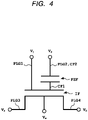
- FIG. 4 is a circuit diagram illustrating an equivalent circuit of the main portion of the semiconductor device SD.
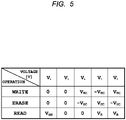
- FIG. 5 is a table showing examples of voltages applied to respective portions of the semiconductor device SD in the write operation, the erase operation, and the read operation.
- V s indicates a voltage applied to the source region SR.
- V d indicates a voltage applied to the drain region DR.
- V w indicates a voltage applied to the well region WR.
- V 1 indicates a voltage applied to the first conductive film CF1 through the first plug PLG1.
- V 2 indicates a voltage applied to the second conductive film CF2 through the second plug PLG2.
- a case in which the polarization state of the ferroelectric film FEF is a first polarization state (upward) is referred to as a "write state”.
- a case in which the polarization state of the ferroelectric film FEF is a second polarization state (downward) that differs from the first polarization state will be described as an "erase state.”
- a threshold voltage of the ferroelectric memory cell in the write state is assumed to be greater than the threshold voltage of the ferroelectric memory cell in the erase state.
- a negative voltage -V EC is applied to the first conductive film CF1
- a positive voltage V EC is applied to the well region WR and the second conductive film CF2.
- the voltage V EC is, for example, 3 V.
- the voltage of each of the source region SR and drain region DR is, for example, 0 V.
- a positive voltage V EC is applied to the first conductive film CF1 while a voltage of the same magnitude is applied to the source region SR and the drain region DR, and a negative voltage -V EC is applied to the well region WR and the second conductive film CF2.
- the polarization state of the ferroelectric film FEF becomes the second polarization state. That is, the ferroelectric memory cell become in the erased state.
- the voltage of each of the source region SR and drain region DR is, for example, 0 V.
- Bias is applied between the source region SR and the drain region DR while a voltage V R of a predetermined magnitude is applied to the first conductive film CF1 and the second conductive film CF2.
- a voltage V dd is applied to the source region SR, and the potentials of the drain region DR and the well region WR are set to 0 V.
- the voltage V dd is, for example, a voltage 1 V. From the viewpoint of preventing the polarization state of the ferroelectric film FEF from changing, the voltage V 1 applied to the first conductive film CF1 and the voltage V 2 applied to the second conductive film CF2 are the same to each other.
- the voltage V R is set to be greater than the threshold voltage of the ferroelectric memory cell in the erase state and smaller than the threshold voltage of the ferroelectric memory cell in the write state. As a result, no current flows in the ferroelectric memory cell in the programmed state, and a current flows in the ferroelectric memory cell in the erased state. In this manner, the state of the ferroelectric memory cell is read out based on the magnitude of the current value flowing in the ferroelectric memory cell.
- the voltage V R is, for example, 0 V.
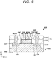
- a semiconductor device cSD (hereinafter also referred to as "a comparative semiconductor device") without the first plug PLG1 reaching the first conductive film CF1 will also be described.
- FIG. 6 is a cross-sectional view illustrating an exemplary configuration of the comparative semiconductor device cSD.
- FIG. 7 is a circuit diagram illustrating an equivalent circuit of a main portion of the semiconductor device cSD.
- a size of each of the insulating film IF, the first conductive film CF1, the ferroelectric film cFEF and the second conductive film cCF2, in a plan view, is the same to each other.
- the comparative semiconductor device cSD does not include the first plug PLG1 configured to directly apply a voltage to the first conductive film CF1. That is, the voltage V 1 is not applied to the first conductive film CF1.
- the write operation is performed, for example, as follows. With a voltage of the same magnitude applied to the source region SR and the drain region DR, a negative voltage -V EC is applied to the well region WR, and a positive voltage V EC is applied to the second conductive film CF2. The erase operation is performed by making the positive and negative of the applied voltage opposite in comparison with the applied voltage of the write operation.
- a voltage is applied to the ferroelectric film cFEF between the well region WR and the second conductive film CF2. That is, through the well region WR, a voltage is applied to the ferroelectric film cFEF.
- a capacitance component corresponding to the ferroelectric film cFEF, and a capacitance component corresponding to the insulating film IF are connected in series between the second conductive film CF2 and the well region WR. Therefore, even when a voltage is applied to the second conductive film CF2, it is divided into the ferroelectric film cFEF and the insulating film IF.
- the voltage applied to the second conductive film CF2 is V 2
- the voltage V 21 distributed to the ferroelectric film cFEF and the voltage V 22 distributed to the insulating film IF are expressed by the following equations (1) and (2), respectively.
- V 21 V 2 / 1 + C 1 / C 2
- V 22 V 2 / 1 + C 2 / C 1
- C 1 is a capacitance value of the capacitance component corresponding to the ferroelectric film cFEF.
- C 2 is a capacitance value of the capacitance component corresponding to the insulating film IF.
- the voltage V 21 distributed to the ferroelectric film cFEF varies depending on the magnitudes of C 1 and C 2 , but is smaller than V 2 . Therefore, in the comparative semiconductor device cSD, during the write operation and erase operation, the applied voltage distributed to the ferroelectric film cFEF may be inadequate. From the viewpoint of increasing the applied voltage distributed to the ferroelectric film cFEF, a mean of decreasing the thickness of the insulating film IF is conceivable in order to increase C 2 of the applied voltage. However, if the thickness of the insulating film IF is too small, the reliability of the semiconductor device cSD is reduced.
- a mean for increasing the thickness of the ferroelectric film cFEF can be considered.
- a mean for increasing V 2 of applied voltages is also conceivable.
- the driving voltage of the semiconductor device cSD increases.
- the semiconductor device SD in the semiconductor device SD according to the present embodiment, a voltage is applied to the ferroelectric film FEF through the first plug PLG1 reaching the first conductive film CF1.
- the voltage applied is not distributed to the insulating film IF. Consequently, the reliability of the semiconductor device SD can be enhanced in the present embodiment compared to the comparative semiconductor device cSD. Further, since the applied voltage does not need to be increased, the driving voltage of the semiconductor device cSD can be reduced.
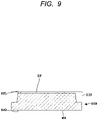
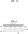
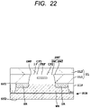
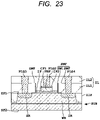
- FIGS. 8 to 23 are cross-sectional views illustrating exemplary steps included in the method of manufacturing the semiconductor device SD.
- the method of manufacturing the semiconductor device SD includes (1) providing a semiconductor wafer SW, (2) forming the insulating film IF, (3) forming the first conductive film CF1, (4) forming an amorphous film AMF, (5) forming the second conductive film CF2, (6) crystallization , (7) a first patterning, (8) forming a sacrificial layer SL, (9) second patterning, (10) forming the sidewall insulating film SWF, (11) forming the source region SR and the drain region DR, (12) forming the first insulating layer IL1, (13) CMP, (14) removing the sacrificial layer SL, (15) forming the second insulating layer IL2, (16) forming the first plug PLG1, the second PLG2, the third plug PLG3, and the fourth plug PLG4.
- the semiconductor wafer SW includes a semiconductor substrate SUB in which the well region WR and the isolation insulating film IIF are formed on the first surface SF1.
- the semiconductor wafer SW may be manufactured or purchased as a commercial product.
- the semiconductor wafer SW is, for example, a silicon wafer.
- the well region WR and the isolation insulating film IIF may be formed in a silicon wafer purchased as a commercial product.
- a method of forming the well region WR is not particularly limited. For example, by ion implantation and activation annealing, the well region WR is formed.
- a method of forming the isolation insulating film IIF is not particularly limited. For example, by burying a recess portion formed on the semiconductor substrate SUB with an insulating film, the isolation insulating film IIF may be formed. Further, by oxidizing a part of the first surface SF1 of the semiconductor substrate SUB by LOCOS method, the isolation insulating film IIF may be formed.
- the insulating film IF is formed on the first surface SF1 of the semiconductor substrate SUB.
- the insulating film IF is formed by, for example, a Chemical Vapor Deposition (CVD) method.
- CVD Chemical Vapor Deposition
- the insulating film IF is not patterned, it is formed on an entire of the first surface SF1 of the semiconductor substrate SUB.
- the first conductive film CF1 is formed on the insulating film IF.
- a method of forming the first conductive film CF1 is, for example, a sputtering method. In this step, the first conductive film CF1 is not patterned, it is formed on an entire of the insulating film IF.
- an amorphous film AMF is formed on the first conductive film CF1.
- the amorphous film AMF is the ferroelectric film FEF before being crystallized.
- the amorphous film AMF is formed by, for example, an Atomic Layer Deposition (ALD) method.
- the crystallization promotion material When the crystallization promotion material is added to the amorphous film AMF, after the first amorphous film is formed, the crystallization promotion material may be formed on the first amorphous film by, for example, a sputtering method. In this case, after forming the crystallization promotion material, a second amorphous film is formed on the first amorphous film. Further, after forming the amorphous film AMF, for example, the crystallize promotion material may be formed in the amorphous film AMF by an ion implantation method.
- the second conductive film CF2 is formed on the amorphous film AMF.
- a method of forming the second conductive film CF2 is, for example, a sputtering method. In this step, the second conductive film CF2 is not patterned and is formed on an entire of the amorphous film AMF.
- the amorphous film AMF is crystallized to form the ferroelectric film FEF.
- a method of crystallization is heat treatment.
- the method of heat treatment is, for example, Rapid Thermal Annealing (RTA) method.
- RTA Rapid Thermal Annealing
- the heating temperature of the amorphous film AMF is, for example, 600 °C or more and 800 °C or less.
- the crystal structure of the ferroelectric film FEF is likely to be monoclinic.
- the amorphous film AMF does not become a ferroelectric film, becomes a paraelectric film.
- the second conductive film CF2 is formed on the amorphous film AMF. Therefore, the ferroelectric film is easily formed by stresses from the second conductive film CF2.
- Another method of the heat treatment is a heat treatment using the following microwaves frequency 1 GHz or more and 10 GHz or less.
- the heating temperature of the amorphous film AMF is, for example, 400 ° C or less.
- the second conductive film CF2 and the ferroelectric film FEF are patterned into a desired pattern. Patterning is performed, for example, by photolithography and etching methods. Although not shown in particular, a resist mask is formed on a region other than a region to be etched.
- a sacrificial layer SL is formed on the first conductive film CF1 so as to cover the second conductive film CF2 and the ferroelectric film FEF.
- the sacrificial layer SL includes, for example, a polycrystalline silicon layer PSL and a hard mask HM formed on the polycrystalline silicon layer PSL.
- the polycrystalline silicon layer PSL is formed, for example, by a CVD method.
- the hard mask HM is formed by, for example, a sputtering method.
- the sacrificial layer SL, the first conductive film CF1 and the insulating film IF are patterned so that the desired pattern is achieved. Patterning is performed, for example, by photolithography and etching methods. Although not shown in particular, a resist mask is formed on a region other than a region to be etched.
- the pair of sidewall insulating film SWF is formed on the first surface SF1 of the semiconductor substrate SUB so as to sandwich a structure consisting of the insulating film IF, the first conductive film CF1 and the sacrificial layer SL, .
- a part of the layer film is removed so that a part located on a sidewall of the structure, of the multi-layer film, remains.
- the part of the multi-layer film is removed by, for example, a photolithography method and an etching method.
- the first surface SF1 of the semiconductor substrate SUB, the source region SR and the drain region DR are formed.
- a method of forming the source region SR and the drain region DR is not particularly limited.
- the source region SR and the drain region DR are formed by ion implantation and activation annealing. Note that, although not particularly shown, in the ion implantation method, a resist mask is formed on a region other than a region where ion implantation is to be performed.
- the first insulating layer IL1 is formed on the semiconductor substrate SUB so as to cover the sacrificial layer SL and the sidewall insulating film SWF.
- a method of forming the first insulating layer IL1 is, for example, a CVD method.
- an upper surface of the first insulating layer IL1 is polished so that the sacrificial layer SL is exposed from the first insulating layer IL1.
- it may be polished part of the sidewall insulating film SWF.
- a part of the sacrificial layer SL may be removed.
- the hard mask HM and a part of the polysilicon layer PSL are removed.
- the sacrificial layer SL is removed.
- the polysilicon layer PSL of the sacrificial layer SL is removed.
- a method of removing the sacrificial layer SL for example, a wet etching method or an isotropic dry etching method.
- An etching solution used for wet etching is, for example, a mixed solution of aqueous ammonia and aqueous hydrogen peroxide.
- the second insulating layer IL2 is formed on the first insulating layer IL1 so as to bury a region surrounded by the pair of sidewall insulating films SWF.
- the insulating layer IL including a first insulating layer IL IL1 and a second IL2 is formed.
- the second insulating layer IL2 is formed on the first conductive film CF1 so as to cover the ferroelectric film FEF and the second conductive film CF2.
- the method of forming the second insulating layer IL2 is, for example, a CVD method.
- the first plug PLG1, the second plug PLG2, the third plug PLG3 and the fourth plug PLG4 are formed in the insulating layer IL.
- the second plug PLG2 penetrates through the second insulating layer IL2 so as not to overlap with the first insulating layer IL1 in plan view.
- the first plug PLG1, the third plug PLG3 and the fourth plug PLG4 penetrate through the first insulating layer IL1 and the second insulating layer IL2.
- a through hole is formed in insulating layer IL, then a conductive material is buried in the through hole.
- each of the first plug PLG1, the second plug PLG2, the third plug PLG3 and the fourth plug PLG4 is formed.
- a wiring layer is formed on the insulating layer IL.
- the semiconductor device SD according to the present embodiment is manufactured by the manufacturing method.
- the first plug PLG1 is formed such that the first plug PLG1 reaches the first conductive film CF1
- the second plug PLG2 is formed through the second conductive film CF2 such that the second plug PLG2 reaches the ferroelectric film FEF.
- a voltage is applied to the ferroelectric film FEF between the first plug PLG1 and the second plug PLG2 without passing through the well region WR. Therefore, in the write operation and the erase operation, the voltage for applying to the ferroelectric film FEF is not divided into the insulating film IF. Voltage of the desired magnitude can be applied to the ferroelectric film FEF. As a result, the reliability of the semiconductor device SD can be enhanced. Further, since the voltage for applying to the ferroelectric film FEF is not divided into the insulating film IF, it is not necessary to increase the applied voltage. Consequently, the present embodiment can reduce the drive voltage of the semiconductor device SD.
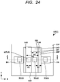
- FIG. 24 is a plan view illustrating an exemplary configuration of a main portion of a semiconductor device mSD1 according to a first modification of the present embodiment.
- FIG. 25 is a cross-sectional view illustrating an exemplary configuration of the main portion of the semiconductor device mSD1.
- FIG. 25 is a cross-sectional view taken along line A-A of FIG. 24 .
- a first plug mPLG1, the second plug PLG2, the third plug PLG3, and the fourth plug PLG4 are disposed along the opposing direction (X direction) in which the source region SR and the drain region DR are opposite to each other.
- the first plug mPLG1, in plan view, is formed between the pair of sidewall insulating films SWF.
- the first plug mPLG1 penetrates through the second insulating layer IL2 without overlapping the first insulating layer IL1 in plan view.
- the distance d1 of the first long side LS1 and the ferroelectric film FEF is greater than the distance d2 of the second long side LS2 and the ferroelectric film FEF. That is, in plan view, the ferroelectric film FEF is closer to the drain region DR than the source region SR.
- an region for forming the first plug mPGL1 is ensured.
- the first plug mPGL1 is disposed in the memory cell, and a region of the memory cell can be reduced.
- the second plug PLG2 penetrates through the second insulating layer IL2 without overlapping the first insulating layer IL1 in plan view.
- a plurality of first plugs mPLG1 may be formed in each of a plurality of memory cells.
- a voltage can be applied to the first conductive film CF1 formed in each of the plurality of memory cells through the first plug mPLG1. Therefore, the accuracy can be improved relative to the control of the memory window and write/erase operations. Consequently, the reliability of the semiconductor device mSD1 can be improved.
- FIG. 26 is a plan view illustrating an exemplary configuration of a main portion of a semiconductor device mSD2 according to a second modification of the present embodiment.
- FIG. 27 is a cross-sectional view illustrating an exemplary configuration of the main portion of the semiconductor device mSD2.
- FIG. 27 is a cross-sectional view taken along line A-A of FIG. 26 .
- the first plug mPLG1 overlaps with the isolation insulating film IIF, and is formed between the first long side LS1 and a ferroelectric film mFEF2 of the first conductive film CF1.
- the ease of manufacturing can be improved.
- the margins for short between the first plug mPGL1 and second plug PGL2 and short between the first plug mPLG1 and the second conductive film mCF2-1 can be increased.
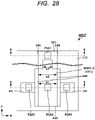
- FIG. 28 is a plan view illustrating an exemplary configuration of a main portion of a semiconductor device mSD3 according to a third modification of the present embodiment.
- FIG. 29 is a cross-sectional view illustrating an exemplary configuration of the main portion of the semiconductor device mSD3.
- FIG. 29 is a cross-sectional view taken along line A-A of FIG. 28 .
- the length (width) w1 of a ferroelectric film mFEF3 located on the region between the source region SR and the drain region DR is substantially the same as the length (width) w2 of the first conductive film CF1 in the X-direction.
- a size of the ferroelectric film mFEF3 is the same as a size of the second conductive film mCF2-2.
- the length (width) w3 of a part located on the isolation insulating film IIF is smaller than the length (width) w2 of the first conductive film CF1.
- the ferroelectric film mFEF3 directly contacts with the sidewall insulating film SWF.
- the w1 is substantially the same as the w2.
- the insulating film IF, the first conductive film CF1, the ferroelectric film mFEF3 and second conductive film CF2 can be processed in a common process. Consequently, the manufacturing cost of the semiconductor device mSD3 can be reduced.
Landscapes
- Engineering & Computer Science (AREA)
- Computer Hardware Design (AREA)
- Power Engineering (AREA)
- Semiconductor Memories (AREA)
- Non-Volatile Memory (AREA)
Applications Claiming Priority (1)
| Application Number | Priority Date | Filing Date | Title |
|---|---|---|---|
| US17/038,784 US20220102558A1 (en) | 2020-09-30 | 2020-09-30 | Semiconductor device |
Publications (1)
| Publication Number | Publication Date |
|---|---|
| EP3979321A1 true EP3979321A1 (de) | 2022-04-06 |
Family
ID=77821575
Family Applications (1)
| Application Number | Title | Priority Date | Filing Date |
|---|---|---|---|
| EP21197279.9A Pending EP3979321A1 (de) | 2020-09-30 | 2021-09-16 | Halbleiterbauelement |
Country Status (6)
| Country | Link |
|---|---|
| US (2) | US20220102558A1 (de) |
| EP (1) | EP3979321A1 (de) |
| JP (1) | JP7611108B2 (de) |
| KR (1) | KR102913840B1 (de) |
| CN (1) | CN114335007A (de) |
| TW (1) | TWI896774B (de) |
Cited By (1)
| Publication number | Priority date | Publication date | Assignee | Title |
|---|---|---|---|---|
| WO2023031144A1 (en) * | 2021-09-01 | 2023-03-09 | International Business Machines Corporation | Transistor gates having embedded metal-insulator-metal capacitors |
Families Citing this family (2)
| Publication number | Priority date | Publication date | Assignee | Title |
|---|---|---|---|---|
| KR20230021517A (ko) * | 2021-08-05 | 2023-02-14 | 삼성전자주식회사 | 반도체 소자, 반도체 소자 어레이 구조, 반도체 소자를 포함하는 뉴로모픽 회로 및 뉴로모픽 회로를 포함하는 컴퓨팅 장치 |
| KR20230043634A (ko) * | 2021-09-24 | 2023-03-31 | 에스케이하이닉스 주식회사 | 강유전층 및 금속 입자가 내장된 절연층을 포함하는 반도체 장치 |
Citations (3)
| Publication number | Priority date | Publication date | Assignee | Title |
|---|---|---|---|---|
| EP1143525A2 (de) * | 2000-03-16 | 2001-10-10 | Yasuo Tarui | Ferroelektrisches nichtschwebendes Speicherelement vom Transistortyp |
| US6750501B2 (en) * | 2001-04-16 | 2004-06-15 | Yasuo Tarui | Transistor type ferroelectric body nonvolatile storage element |
| JP2019201172A (ja) | 2018-05-18 | 2019-11-21 | ルネサスエレクトロニクス株式会社 | 半導体装置およびその製造方法 |
Family Cites Families (9)
| Publication number | Priority date | Publication date | Assignee | Title |
|---|---|---|---|---|
| JP3160325B2 (ja) * | 1991-09-26 | 2001-04-25 | ローム株式会社 | 半導体記憶素子 |
| US5523964A (en) * | 1994-04-07 | 1996-06-04 | Symetrix Corporation | Ferroelectric non-volatile memory unit |
| JP4459335B2 (ja) * | 1999-10-19 | 2010-04-28 | キヤノン株式会社 | 強誘電体トランジスタ型不揮発性記憶素子とその製造方法 |
| CN1170320C (zh) | 2000-03-13 | 2004-10-06 | 松下电器产业株式会社 | 半导体装置及其制造方法 |
| JP3593046B2 (ja) * | 2000-03-13 | 2004-11-24 | 松下電器産業株式会社 | 半導体装置 |
| US6720596B2 (en) * | 2000-10-17 | 2004-04-13 | Matsushita Electric Industrial Co., Ltd. | Semiconductor device and method for driving the same |
| US10686072B2 (en) * | 2016-12-14 | 2020-06-16 | Taiwan Semiconductor Manufacturing Co., Ltd. | Semiconductor device and manufacturing methods thereof |
| US10896979B2 (en) * | 2017-09-28 | 2021-01-19 | International Business Machines Corporation | Compact vertical injection punch through floating gate analog memory and a manufacture thereof |
| US10707295B2 (en) * | 2018-09-17 | 2020-07-07 | Taiwan Semiconductor Manufacturing Co., Ltd. | Memory device and fabrication method thereof |
-
2020
- 2020-09-30 US US17/038,784 patent/US20220102558A1/en not_active Abandoned
-
2021
- 2021-09-16 EP EP21197279.9A patent/EP3979321A1/de active Pending
- 2021-09-23 CN CN202111114186.XA patent/CN114335007A/zh active Pending
- 2021-09-27 KR KR1020210127056A patent/KR102913840B1/ko active Active
- 2021-09-27 JP JP2021156924A patent/JP7611108B2/ja active Active
- 2021-09-27 TW TW110135768A patent/TWI896774B/zh active
-
2023
- 2023-02-01 US US18/163,046 patent/US12166123B2/en active Active
Patent Citations (3)
| Publication number | Priority date | Publication date | Assignee | Title |
|---|---|---|---|---|
| EP1143525A2 (de) * | 2000-03-16 | 2001-10-10 | Yasuo Tarui | Ferroelektrisches nichtschwebendes Speicherelement vom Transistortyp |
| US6750501B2 (en) * | 2001-04-16 | 2004-06-15 | Yasuo Tarui | Transistor type ferroelectric body nonvolatile storage element |
| JP2019201172A (ja) | 2018-05-18 | 2019-11-21 | ルネサスエレクトロニクス株式会社 | 半導体装置およびその製造方法 |
Non-Patent Citations (2)
| Title |
|---|
| KIM SI JOON ET AL: "Ferroelectric Hf0.5Zr0.5O2Thin Films: A Review of Recent Advances", JOM: JOURNAL OF METALS, SPRINGER NEW YORK LLC, UNITED STATES, vol. 71, no. 1, 28 September 2018 (2018-09-28), pages 246 - 255, XP036663722, ISSN: 1047-4838, [retrieved on 20180928], DOI: 10.1007/S11837-018-3140-5 * |
| SCHROEDER UWE ET AL: "Lanthanum-Doped Hafnium Oxide: A Robust Ferroelectric Material", INORGANIC CHEMISTRY, vol. 57, no. 5, 5 March 2018 (2018-03-05), Easton , US, pages 2752 - 2765, XP055821760, ISSN: 0020-1669, Retrieved from the Internet <URL:https://pubs.acs.org/doi/pdf/10.1021/acs.inorgchem.7b03149> DOI: 10.1021/acs.inorgchem.7b03149 * |
Cited By (2)
| Publication number | Priority date | Publication date | Assignee | Title |
|---|---|---|---|---|
| WO2023031144A1 (en) * | 2021-09-01 | 2023-03-09 | International Business Machines Corporation | Transistor gates having embedded metal-insulator-metal capacitors |
| US11929404B2 (en) | 2021-09-01 | 2024-03-12 | International Business Machines Corporation | Transistor gates having embedded metal-insulator-metal capacitors |
Also Published As
| Publication number | Publication date |
|---|---|
| KR102913840B1 (ko) | 2026-01-19 |
| TWI896774B (zh) | 2025-09-11 |
| US20230187550A1 (en) | 2023-06-15 |
| TW202230687A (zh) | 2022-08-01 |
| JP7611108B2 (ja) | 2025-01-09 |
| US20220102558A1 (en) | 2022-03-31 |
| JP2022058238A (ja) | 2022-04-11 |
| KR20220044121A (ko) | 2022-04-06 |
| CN114335007A (zh) | 2022-04-12 |
| US12166123B2 (en) | 2024-12-10 |
Similar Documents
| Publication | Publication Date | Title |
|---|---|---|
| JP7594650B2 (ja) | 半導体装置の製造方法 | |
| US12166123B2 (en) | Semiconductor device | |
| US6288431B1 (en) | Semiconductor device and a method of manufacturing the same | |
| US11289510B2 (en) | Semiconductor device including ferroelectric film and method of manufacturing the same | |
| JP2009170511A (ja) | 半導体素子及び半導体装置 | |
| US11646376B2 (en) | Semiconductor device and method of manufacturing the same | |
| US20210013328A1 (en) | Semiconductor device and method of manufacturing the semiconductor device | |
| US11335702B1 (en) | Semiconductor device and method of manufacturing the same | |
| US6580119B1 (en) | Stacked gate field effect transistor (FET) device | |
| US20170278938A1 (en) | Semiconductor device and method for manufacturing the same | |
| US12107138B2 (en) | Semiconductor device and method of manufacturing the same | |
| US20230037374A1 (en) | Semiconductor device and method of manufacturing the same | |
| US6787842B1 (en) | Method for operating a stacked gate field effect transistor (FET) device |
Legal Events
| Date | Code | Title | Description |
|---|---|---|---|
| PUAI | Public reference made under article 153(3) epc to a published international application that has entered the european phase |
Free format text: ORIGINAL CODE: 0009012 |
|
| STAA | Information on the status of an ep patent application or granted ep patent |
Free format text: STATUS: THE APPLICATION HAS BEEN PUBLISHED |
|
| AK | Designated contracting states |
Kind code of ref document: A1 Designated state(s): AL AT BE BG CH CY CZ DE DK EE ES FI FR GB GR HR HU IE IS IT LI LT LU LV MC MK MT NL NO PL PT RO RS SE SI SK SM TR |
|
| STAA | Information on the status of an ep patent application or granted ep patent |
Free format text: STATUS: REQUEST FOR EXAMINATION WAS MADE |
|
| 17P | Request for examination filed |
Effective date: 20221004 |
|
| RBV | Designated contracting states (corrected) |
Designated state(s): AL AT BE BG CH CY CZ DE DK EE ES FI FR GB GR HR HU IE IS IT LI LT LU LV MC MK MT NL NO PL PT RO RS SE SI SK SM TR |