EP3977451B1 - Einschalten eines speicherkerns mit reduziertem spitzenstrom - Google Patents
Einschalten eines speicherkerns mit reduziertem spitzenstrom Download PDFInfo
- Publication number
- EP3977451B1 EP3977451B1 EP20747197.0A EP20747197A EP3977451B1 EP 3977451 B1 EP3977451 B1 EP 3977451B1 EP 20747197 A EP20747197 A EP 20747197A EP 3977451 B1 EP3977451 B1 EP 3977451B1
- Authority
- EP
- European Patent Office
- Prior art keywords
- power supply
- core
- supply rail
- transistor
- memory
- Prior art date
- Legal status (The legal status is an assumption and is not a legal conclusion. Google has not performed a legal analysis and makes no representation as to the accuracy of the status listed.)
- Active
Links
Images



Classifications
-
- G—PHYSICS
- G11—INFORMATION STORAGE
- G11C—STATIC STORES
- G11C5/00—Details of stores covered by group G11C11/00
- G11C5/14—Power supply arrangements, e.g. power down, chip selection or deselection, layout of wirings or power grids, or multiple supply levels
-
- G—PHYSICS
- G11—INFORMATION STORAGE
- G11C—STATIC STORES
- G11C5/00—Details of stores covered by group G11C11/00
- G11C5/14—Power supply arrangements, e.g. power down, chip selection or deselection, layout of wirings or power grids, or multiple supply levels
- G11C5/148—Details of power up or power down circuits, standby circuits or recovery circuits
-
- H—ELECTRICITY
- H03—ELECTRONIC CIRCUITRY
- H03K—PULSE TECHNIQUE
- H03K17/00—Electronic switching or gating, i.e. not by contact-making and –breaking
- H03K17/28—Modifications for introducing a time delay before switching
-
- H—ELECTRICITY
- H03—ELECTRONIC CIRCUITRY
- H03K—PULSE TECHNIQUE
- H03K17/00—Electronic switching or gating, i.e. not by contact-making and –breaking
- H03K17/30—Modifications for providing a predetermined threshold before switching
-
- G—PHYSICS
- G11—INFORMATION STORAGE
- G11C—STATIC STORES
- G11C11/00—Digital stores characterised by the use of particular electric or magnetic storage elements; Storage elements therefor
- G11C11/21—Digital stores characterised by the use of particular electric or magnetic storage elements; Storage elements therefor using electric elements
- G11C11/34—Digital stores characterised by the use of particular electric or magnetic storage elements; Storage elements therefor using electric elements using semiconductor devices
- G11C11/40—Digital stores characterised by the use of particular electric or magnetic storage elements; Storage elements therefor using electric elements using semiconductor devices using transistors
- G11C11/41—Digital stores characterised by the use of particular electric or magnetic storage elements; Storage elements therefor using electric elements using semiconductor devices using transistors forming static cells with positive feedback, i.e. cells not needing refreshing or charge regeneration, e.g. bistable multivibrator or Schmitt trigger
- G11C11/413—Auxiliary circuits, e.g. for addressing, decoding, driving, writing, sensing, timing or power reduction
- G11C11/417—Auxiliary circuits, e.g. for addressing, decoding, driving, writing, sensing, timing or power reduction for memory cells of the field-effect type
-
- G—PHYSICS
- G11—INFORMATION STORAGE
- G11C—STATIC STORES
- G11C5/00—Details of stores covered by group G11C11/00
- G11C5/06—Arrangements for interconnecting storage elements electrically, e.g. by wiring
- G11C5/063—Voltage and signal distribution in integrated semi-conductor memory access lines, e.g. word-line, bit-line, cross-over resistance, propagation delay
Definitions
- This application relates to memories, and more particularly to a memory with reduced peak current during power-up.
- Each bitcell in a static random access memory (SRAM) are active latches a bit through a pair of cross-coupled inverters.
- SRAM static random access memory
- DRAM dynamic random access memory
- an SRAM bitcell is powered and can thus drive out a bit result during a read operation.
- SRAM is thus significantly faster than DRAM due to the active nature of the bitcells.
- the powering-up of the bitcells in an SRAM requires an appreciable amount of charge. The amount of charge required at power-up scales with the number of bitcells for a particular memory. The charge is supplied by a core power supply rail carrying a core power supply voltage for the bitcells.
- the core power supply Prior to power-up, the core power supply is isolated from the bitcells through one or more power switch transistors. It is conventional to switch on all of the power switch transistors at power-up.
- the pair of cross-coupled inverters in each bitcell must resolve to a stable, latched state. In that latched state, the output node of one cross-coupled inverter is driven high to the core power supply voltage whereas the remaining cross-coupled inverter's output node remains discharged. The charging of all the output nodes results in a significant peak input current to the memory core during power-up that can damage the memory.
- US 9 564 180 B1 describing a memory device comprising memory banks, power gates, and bank wake-up circuits.
- Each of the memory banks has a core voltage supply.
- the power gates are coupled to the memory banks for charging the core voltage supplies and have a plurality of powering modes.
- the bank wake-up circuits are coupled to the power gates for selecting one of the plurality of power modes for charging the memory banks during a wake-up mode.
- the bank wake-up circuits sense the core voltage supplies during the wake-up mode.
- the bank wake-up circuits serially charge the memory banks as a function of the sensed core voltage supplies of the memory banks.
- US 2018/174643 A1 describing a dual rail device including a first power domain circuit coupled to a first power supply through a first header control switch and a second power domain circuit coupled to a second power supply.
- the first and second power supplies have different steady-state voltage levels.
- the first power domain circuit is interfaced to the second power domain circuit.
- the device also includes a power detector circuit for providing a control signal for the first header control switch responsive to a voltage level of the second power supply.
- a memory includes: an external power supply rail; a first core power supply rail configured to provide power to a first plurality of bitcells; a first power switch transistor coupled between the first core power supply rail and the eternal power supply rail; a second core power supply rail configured to provide power to a second plurality of bitcells; a second power switch transistor coupled between the second core power supply rail and the external power supply rail; and a control transistor having a gate connected to the first core power supply rail, wherein the second power switch transistor is configured to switch on in response to a switch on of the control transistor.
- a method of powering up a memory includes the acts of: switching on a first power switch transistor to connect a first core power supply rail for a first core of bitcells to an external power supply rail to charge the first core power supply rail from ground to a core power supply voltage, wherein the core power supply voltage is greater than a threshold voltage for a control transistor; switching on the control transistor responsive to the first core power supply rail charging above the threshold voltage; and responsive to the switching on of the control transistor, switching on a second power switch transistor to connect a second core power supply rail for a second core bitcells to the external power supply rail to charge the second core power supply rail from ground to the core power supply voltage.
- a memory includes: a plurality of bitcells arranged into a plurality of cores, wherein the cores are arranged according to a power-up order; a plurality of power supply rails corresponding to the plurality of cores, each power supply rail being configured to power the corresponding core; and a plurality of control transistors corresponding to the plurality of cores, wherein each control transistor is configured to control a power up of the control transistor's core, and wherein a gate for the control transistor in each successive core in the power-up order is connected to the power supply rail for a preceding core in the power-up order.
- the power supply to the bitcells is segregated by its input/output (IO).
- IO input/output
- bitcells it is traditional for bitcells to be arranged by rows and columns. Each row is addressed by a corresponding word line whereas each column is addressed by a corresponding pair of bit lines.
- a sense amplifier senses a voltage difference that develops across the bit line pair for an addressed column.
- the sense amplifier typically has a wider pitch than the bit line pitch so it is conventional for several columns to be multiplexed through a column multiplexer to a single sense amplifier.
- a read output data latch (the IO) latches a bit decision from the sense amplifier for the selected column. The power supply segregation thus applies to all the bitcells in the columns that are multiplexed to a read output data latch.
- the rows and columns for a memory are typically arranged into subarrays designated as memory banks.
- Each memory bank has its own set of read output data latches, arranged from a zeroth read output data latch to a final read output data latch.
- the number of read output data latches for a memory bank depends upon the word size for the memory bank. For example, if the word size is sixty-four bits wide, the memory bank would include sixty-four read output data latches.
- the number of independent core power supply rails for a memory bank corresponds on a one-to-one basis with the number of read output data latches. In the previous example of sixty-four read output data latches, the memory bank would have sixty-four different core power supply rails. These rails are powered up sequentially. Each core power supply rail supplies the core power supply to the bitcells in the columns that are multiplexed onto the corresponding read output data latch.
- FIG. 1 An example memory core 100 for an ith read output data latch 130 is shown in Figure 1 .
- the ⁇ ith> designation for read output data latch 130 refers to its bit position within the word formed by the collection of read output data latches for a corresponding memory. For example, the number of bits in the word may range from a zeroth bit to an (M-1)th bit, where M is the positive integer for the word width.
- the term "core” refers to the bitcells addressed by the columns that are multiplexed onto a single read output data latch.
- the column multiplexing is an N:1 multiplexing through a column multiplexer 125.
- N columns in core 100 There is thus N columns in core 100 ranging from a zeroth column (Column 0) to an (N-1)th column (Column N).
- the number of bitcells within a single column depends upon the number of rows for the memory bank. For example, if the memory bank that includes core 100 has thirty-two rows corresponding to thirty-two word lines, a single column would have thirty-two bitcells. In column 0 there is thus a first bitcell 105 corresponding to the first row. Each remaining row would also have a corresponding bitcell. For illustration clarity, only bitcell 105 and also a final bitcell 110 for the final row are shown in column 0.
- the (N-1)th column includes a plurality of bitcells ranging from a first bitcell 115 for the first row to a final bitcell 120 for the final row.
- the total number of bitcells for a core such as core 100 thus depends not only upon the number of rows for the core's memory bank but also upon the column multiplexing. In embodiments without column multiplexing, the number of bitcells per core would equal the number of rows. If the column multiplexing is 2: 1, the number of bitcells per core would be twice the number of rows. Similarly, if the column multiplexing is 4: 1, the number of bitcells per core would be four times the number of rows.
- the number of bitcells per core is a product of the number of rows for the memory bank and the order of the column multiplexing.
- Each bitcell in core 100 is supplied by the same core power supply rail VDD Core ⁇ i>.
- the ⁇ ith> designation for the core power supply rail corresponds to the ⁇ ith> designation for read output data latch 130.
- a memory that successively powers up the various cores in each memory bank. For example, suppose a memory has a pair of memory banks. The cores in a first one of the memory banks are successively powered up. Once the succession reaches a final one of the cores in the first memory bank, the succession proceeds for the cores in the remaining second memory bank. If a memory has additional memory banks, the succession for the cores would extend across these additional memory banks. The power-up succession would then proceed across the cores in one memory bank to another until all the cores in all the memory banks are powered up.
- the succession across the cores is not based upon any rigid fixed delays but instead exploits the ramping up of the core power supply from ground to its final charged state.
- Each core power supply rail couples through a corresponding power switch transistor to an external power supply rail.
- the core power supply rail is charged to a core power supply voltage supplied by the external power supply rail.
- the core power supply voltage will thus charge from ground to its fully-charged state when the power switch transistor is switched on.
- the memory architecture disclosed herein advantageously exploits the charging of the core power supply voltage from ground to its fully-charged state by using this charging of the core power supply voltage to control when a successive core begins charging.
- the term "external power supply rail” refers to any suitable power supply rail that is isolated from the core power supply rail through a corresponding power switch transistor.
- an integrated circuit including a memory as disclosed herein will have various power supply rails for distributing power supply voltages to the assorted components within the integrated circuit.
- the external power supply rail may be a global power supply rail that provides the core power supply voltage to other components besides the memory.
- the external power supply rail may be dedicated to the distribution of the core power supply voltage to the memory.
- the cores within a memory bank are arranged from a first core to a final core.
- the core power supply from a preceding core controls whether the power switch transistor conducts to power the core.
- the power switch transistor for a core may be an n-type metal-oxide semiconductor (NMOS) transistor.
- NMOS metal-oxide semiconductor
- the core power supply voltage from the preceding core will begin to switch on the power switch transistor for the current core once the core power supply voltage from the preceding core reaches the threshold voltage for the power switch transistor.
- NMOS n-type metal-oxide semiconductor
- PMOS p-type metal-oxide switch
- a "current core” refers to the core currently being powered on in the succession. As the succession proceeds a current core becomes the preceding core to another current core. However, the very first core in the first memory bank that is being powered on has no preceding core before it. A control signal controls whether the core power supply for this first core powers on. For each remaining core in the power-on succession, it is the core power supply for the preceding core that controls whether the core's power supply voltage begins powering up. For example, for a second core in the power-up succession, it is the first core's power supply voltage that controls the charging of the second core's power supply voltage. For a third core in the power-up succession, it is the second core's power supply voltage that controls the charging of the third core's power supply voltage, and so on throughout the power-on succession.
- the core power supply voltage from the preceding core drives the gate of an NMOS control transistor in the current core.
- the control transistor in the current core switches on to ground the gate of the PMOS power switch transistor for the current core.
- This grounding of the gate for the power switch transistor switches on the power switch transistor so that the current core's power supply voltage begins charging.
- this current core becomes the preceding core for a new current core in the power-on succession.
- the power-on succession may be deemed to correspond to an integer succession: a first core, a second core, a third core, a fourth core, and so on.
- the charging of the core power supply voltage for an ith core to the threshold voltage thus determines when the core power supply voltage for the (i + 1)th core begins charging, where i is a positive integer within the integer succession.
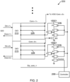
- a memory bank 200 including a plurality of cores that are powered-on according to an embodiment of the power-on succession disclosed herein is shown in Figure 2 .
- Each core includes a plurality of bitcells (not illustrated) as discussed with regard to core 100 of Figure 1 .
- core ⁇ 0> includes the bitcells in the columns addressed by a zeroth read output data latch. These bitcells are powered by a core ⁇ 0> power supply rail 220.
- the zeroth read output data latch and other addressing components such as a word line decoder and column address decoder are represented by a global input/output (GIO) circuit 215 for core ⁇ 0>.
- GIO global input/output
- GIO circuit 215 receives a zeroth bit Din ⁇ 0 of an input word to be written to memory bank 200. Depending upon the addressing, this zeroth bit is then written to one of the bitcells in core ⁇ 0>.
- GIO circuit 215 outputs a zeroth bit Dout ⁇ 0> of the output word being read from memory bank 200.
- core ⁇ 1> includes all the bitcells corresponding to a first read output data latch as represented by a GIO circuit 210.
- GIO circuit 210 receives the first bit of the input word and outputs the first bit of the output word.
- a controller 230 asserts a control signal that drives a gate of an NMOS control transistor M1 for core ⁇ 0>.
- a drain of control transistor M1 connects to a source of an NMOS transistor M2 having a drain connected to a drain of a PMOS transistor P1.
- a source of transistor P1 connects a drain of another PMOS transistor P2 having a source connected to an external power supply rail 235 supplying an external power supply voltage vddehx.
- Transistors P1 and P2 may be replaced by a single PMOS transistor in alternative embodiments.
- An active low sleep signal (Slp_core_n) drives the gates of transistors M2, P1, and P2.
- the source of control transistor M1 connects to ground so that the source of transistor M2 is grounded when the control signal is asserted.
- Transistors P2, P1, and M1 thus act as an inverter to invert the sleep signal while the control signal is asserted.
- the sleep signal is asserted high to the external power supply voltage vddhx.
- the inverter formed by transistors M1, P2, and P1 thus invert this high value for the sleep signal so that the drains of transistors P1 and M2 are grounded.
- These drain nodes are tied to a gate of a PMOS power switch transistor P3 having its source connected to external power supply rail 235 and a drain connected to a core ⁇ 0> power supply rail 220.
- core ⁇ 0> power supply rail 220 Prior to power-up, the voltage of core ⁇ 0> power supply rail 220 is at ground. But in response to the switching on of power switch transistor P3, core ⁇ 0> power supply rail 220 charges up to the core power supply voltage vddehx carried on external power supply rail 235.
- core ⁇ 0> power supply rail 220 is connected to a gate of an NMOS control transistor M3 for core ⁇ 1>.
- first control transistor M3, an NMOS transistor M4, a PMOS transistor P4, a PMOS transistor P5, and a PMOS first power switch transistor P6 are all arranged analogously as discussed for their counterpart transistors M1, M2, P1, P2, and P3 in core ⁇ 0>.
- transistors P5, P4, and transistor M4 function as an inverter when control transistor M3 switches on in response to core ⁇ 0> power supply rail 220 being charged above the threshold voltage for control transistor M3.
- transistors P5 and P4 may be replaced by a single PMOS transistor in alternative embodiments.
- the active low sleep signal Slp_core_n drives the gates of transistors M4, P4, and P5.
- control transistor M3 discharging the source of transistor M4, transistors M4, P4, and P5 function as an inverter to invert the charged state of the sleep signal during normal operation so as to ground the gate of power switch transistor P6.
- Power switch transistor P6 will thus start conducting when the core ⁇ 0> power supply rail 220 is charged above the threshold voltage for control transistor M3.
- the source of power switch transistor P6 is tied to external power supply rail 235 whereas its drain is connected to a core ⁇ 1> power supply rail 225.
- Core ⁇ 1> power supply rail 225 supplies the core power supply voltage to all the bitcells in core ⁇ 1>.
- Core ⁇ 1> power supply rail 225 will then charge from ground to the core power supply voltage vddehx. As it does so, it will pass the threshold voltage for a control transistor in a core ⁇ 2> (not illustrated) such that the power supply rail for this second core will begin to charge towards the power supply voltage vddehx. In turn, the powering up of the second core triggers the powering up of a third core and so on.
- each bank has sixty-four cores, ranging from a core ⁇ 0> to a core ⁇ 63>.
- Core ⁇ 0> in bank 0 is analogous to core ⁇ 0> in memory bank 200 in that it is this core that will respond to the assertion of the control signal.
- the core power supply voltage As the core power supply voltage then rises for core ⁇ 0> above the threshold voltage, it triggers the power up of the core power supply voltage for core ⁇ 1> in bank 0.
- the successive power-up of the cores continues until the final core ⁇ 63> in bank 0 begins to power up.
- the power supply rail in this sixty-third core is tied to a control transistor (not illustrated) in core ⁇ 0> in bank 1.
- the successive power-up of the cores in bank 0 will thus trigger a successive power-up of the cores in bank 1 until a final core ⁇ 63> is bank 1 is fully charged.
- the order is arbitrary and can be varied in alternative embodiments.
- the order need not be from core to core but instead may be from one group of cores to another.
- the power supply rail for successive groups of two cores may be tied together such that a pair of cores is powered up in common. Once the core power supply voltage for a first pair of cores reaches the threshold voltage for a second pair of cores, the power-up of the second pair of cores is triggered, and so on.
- the method includes an act 400 of switching on a first power switch transistor to connect a first power supply rail for a first memory core to an external power supply rail to charge the first power supply rail from ground to a core power supply voltage, wherein the core power supply voltage is greater than a threshold voltage for a first control transistor.
- the switching on of power switch transistor P3 in core ⁇ 0> of memory bank 200 is an example of act 400.
- the method includes an act 405 of switching on the first control transistor responsive to the first power supply rail charging above the threshold voltage.
- the switching on of control transistor M3 in core ⁇ 1> of memory bank 200 is an example of act 405.
- the method includes an act 410 that is responsive to the switching on of the first control transistor and includes switching on a second power switch transistor to connect a second power supply rail for a second memory core to the external power supply rail to charge the second power supply rail from ground to the core power supply voltage.
- act 410 The charging of core ⁇ 1> power supply rail 225 in memory bank 200 is an example of act 410.
- a memory with a successive power-up of cores as disclosed herein may be incorporated into a wide variety of electronic systems.
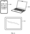
- a cell phone 500, a laptop 505, and a tablet PC 510 may all include a memory having a successive power-up of cores in accordance with the disclosure.
- Other exemplary electronic systems such as a music player, a video player, a communication device, and a personal computer may also be configured with memories constructed in accordance with the disclosure.
Landscapes
- Engineering & Computer Science (AREA)
- Power Engineering (AREA)
- Microelectronics & Electronic Packaging (AREA)
- Computer Hardware Design (AREA)
- Static Random-Access Memory (AREA)
Claims (13)
- Ein Speicher (200), der Folgendes aufweist:eine externe Leistungsversorgungsschiene (235);eine erste Kernleistungsversorgungsschiene (220), die konfiguriert ist zum Vorsehen von Leistung an eine Vielzahl von Bitzellen;einen ersten Leistungsschalttransistor (P3), der an die erste Kernleistungsversorgungsschiene und die externe Leistungsversorgungsschiene gekoppelt ist;einen ersten Steuertransistor (M1), der konfiguriert ist sich einzuschalten, und zwar ansprechend auf ein Steuersignal, wobei der erste Leistungsschalttransistor konfiguriert ist sich einzuschalten, und zwar ansprechend auf das Einschalten des ersten Steuertransistors;eine zweite Kernleistungsversorgungsschiene (225), die konfiguriert ist zum Vorsehen von Leistung an eine zweite Vielzahl von Bitzellen;einen zweiten Leistungsschalttransistor (P6), der zwischen die zweite Kernleistungsversorgungsschiene und die externe Leistungsversorgungsschiene gekoppelt ist;einen zweiten Steuertransistor (M3), mit einem Gate, das mit der ersten Kernleistungsversorgungsschiene verbunden ist, wobei der zweite Leistungsschalttransistor konfiguriert ist sich einzuschalten, und zwar ansprechend auf ein Einschalten des zweiten Steuertransistors; undeinen Inverter (M4, P4, P5), der konfiguriert ist zum Invertieren eines Aktiv-Niedrig-Ruhesignals, wobei die Drain des zweiten Steuertransistors mit einem Masseknoten für den Inverter verbunden ist, und wobei ein Ausgangsknoten des Inverters mit dem Gate des zweiten Leistungsschalttransistor verbunden ist.
- Speicher nach Anspruch 1, wobei der zweite Leistungsschalttransistor ein p-Typ-Metalloxidhalbleiter- bzw. PMOS-Transistor (PMOS = p-type metal-oxide semiconductor) ist und der zweite Steuertransistor ein NMOS-Transistor ist, der eine Source hat, die mit Masse verbunden ist, und eine Drain, die an ein Gate des zweiten Leistungsschalttransistors gekoppelt ist.
- Speicher nach Anspruch 1, wobei der erste Leistungsschalttransistor ein PMOS-Transistor ist, der eine Source hat, die mit der externen Leistungsversorgungsschiene verbunden ist, und eine Drain, die mit der ersten Leistungsversorgungsschiene verbunden ist, und wobei der erste Steuertransistor ein NMOS-Transistor ist, der eine Source hat, die mit Masse verbunden ist, und eine Drain, die an ein Gate des ersten Leistungsschalttransistors gekoppelt ist.
- Speicher nach Anspruch 3, der weiter Folgendes aufweist:
einen zweiten Inverter, der konfiguriert ist zum Invertieren des Aktiv-Niedrig-Ruhesignals, wobei die Drain des ersten Steuertransistors mit einem Masseknoten für den zweiten Inverter verbunden ist, und wobei ein Ausgangsknoten des zweiten Inverters mit dem Gate des ersten Leistungsschalttransistors verbunden ist. - Speicher nach Anspruch 1, der weiter Folgendes aufweist:eine dritte Kernleistungsversorgungsschiene, die konfiguriert ist zum Vorsehen von Leistung an eine dritte Vielzahl von Bitzellen;einen dritten Leistungsschalttransistor, der zwischen die dritte Kernleistungsversorgungsschiene und die externe Leistungsversorgungsschiene gekoppelt ist; undeinen zweiten Steuertransistor mit einem Gate, das mit der zweiten Kernleistungsversorgungsschiene verbunden ist, wobei der dritte Leistungsschalttransistor konfiguriert ist sich einzuschalten, und zwar ansprechend auf ein Einschalten des zweiten Steuertransistors.
- Speicher nach Anspruch 5, wobei der dritte Leistungsschalttransistor ein PMOS-Transistor ist, und der zweite Steuertransistor ein NMOS-Transistor ist mit einer Source, die mit Masse verbunden ist, und einer Drain, die an ein Gate des dritten Leistungsschalttransistor gekoppelt ist.
- Speicher nach Anspruch 1, wobei die erste Vielzahl von Bitzellen und die zweite Vielzahl von Bitzellen in einer ersten Speicherbank angeordnet sind, die eine finale Vielzahl von Bitzellen hat, die konfiguriert ist durch eine finale Leistungsversorgungsschiene mit Leistung versorgt zu werden, wobei der Speicher weiter Folgendes aufweist:
eine zweite Speicherbank, die Folgendes aufweist:eine dritte Vielzahl von Bitzellen, die konfiguriert sind durch eine dritte Kernleistungsversorgungsschiene mit Leistung versorgt zu werden;einen dritten Leistungsschalttransistor, der zwischen die dritte Kernleistungsversorgungsschiene und die externe Leistungsversorgungsschiene gekoppelt ist; undeinen dritten Steuertransistor mit einem Gate, das mit der finalen Leistungsversorgungsschiene verbunden ist, wobei der dritte Leistungsschalttransistor konfiguriert ist sich einzuschalten, und zwar ansprechend auf ein Einschalten des zweiten Steuertransistors. - Speicher nach Anspruch 1, wobei die erste Vielzahl von Bitzellen in eine erste Vielzahl von Spalten angeordnet ist, wobei die zweite Vielzahl von Bitzellen in eine zweite Vielzahl von Spalten angeordnet ist.
- Ein Verfahren zum Hochfahren eines Speichers (200), das Folgendes aufweist:Einschalten eines ersten Steuertransistors (M1) ansprechend auf ein Steuersignal, Einschalten (400) eines ersten Leistungsschalttransistors (P3) zum Verbinden einer ersten Kernleistungsversorgungsschiene (220) für einen ersten Kern von Bitzellen mit einer externen Leistungsversorgungsschiene (235) zum Laden der ersten Kernleistungsversorgungsschiene von Masse auf eine Kernleistungsversorgungsspannung, wobei die Kernleistungsversorgungsspannung größer ist als eine Schwellenwertspannung für einen zweiten Steuertransistor (M3), wobei das Einschalten des ersten Leistungsschalttransistors ansprechend auf das Einschalten des ersten Steuertransistors stattfindet;Einschalten des zweiten Steuertransistors ansprechend darauf, dass die erste Kernleistungsversorgungsspannung über die Schwellenwertspannung lädt, um Masse an einen Inverter (M4, P4, P5) zu liefern;Invertieren eines Ruhesignals (Slp_core_n) durch den Inverter, während der zweite Steuertransistor eingeschaltet ist und während das Ruhesignal auf die Kernleistungsversorgungsspannung geladen ist, um ein Inverterausgangssignal zu entladen; undansprechend auf das Entladen des Inverterausgangssignals, Einschalten eines zweiten Leistungsschalttransistors (P6) zum Verbinden einer zweiten Kernleistungsversorgungsschiene (225) für einen zweiten Kern von Bitzellen mit der externen Leistungsversorgungsschiene zum Laden der zweiten Kernleistungsversorgungsschiene von Masse auf die Kernleistungsversorgungsspannung;Invertieren des Ruhesignals durch den Inverter, während der zweite Steuertransistor eingeschaltet ist, und während das Ruhesignal entladen wird, zum Laden des ersten Inverterausgangssignals auf die Kernleistungsversorgungsspannung; undansprechend auf das Laden des ersten Inverterausgangssignals auf die Kernleistungsversorgungsspannung, Ausschalten des zweiten Leistungsschalttransistors.
- Verfahren nach Anspruch 9, wobei der erste Kern von Bitzellen und der zweite Kern von Bitzellen in einer ersten Bank für den Speicher angeordnet sind, wobei das Verfahren weiter Folgendes aufweist:Einschalten einer finalen Kernleistungsversorgungsschiene in der ersten Bank für den Speicher von Masse auf die Kernleistungsversorgungsspannung;Einschalten eines dritten Steuertransistors ansprechend darauf, dass die finale Kernleistungsversorgungsspannung über die Schwellenwertspannung lädt; undansprechend auf das Einschalten des dritten Steuertransistors, Einschalten eines dritten Leistungsversorgungsschalttransistors zum Verbinden einer dritten Leistungsversorgungsschiene für einen dritten Kern von Bitzellen in einer zweiten Bank für den Speicher mit der externe Leistungsversorgungsschiene zum Laden der dritten Leistungsversorgungsschiene von Masse auf die Kernleistungsversorgungsspannung.
- Verfahren nach Anspruch 10, das weiter Folgendes aufweist:
sukzessives Einschalten einer Vielzahl von zusätzlichen Kernen in der zweiten Bank für den Speicher gemäß einer Einschaltreihenfolge, wobei sich jeder sukzessive zusätzliche Kern einschaltet ansprechend darauf, dass eine Kernleistungsversorgung für einen vorhergehenden zusätzlichen Kern über die Schwellenwertspannung ansteigt. - Verfahren nach Anspruch 9, das weiter Folgendes aufweist:Einschalten eines dritten Steuertransistors ansprechend darauf, dass die zweite Kernleistungsversorgungsschiene über die Schwellenwertspannung lädt; undansprechend auf das Einschalten des dritten Steuertransistors, Einschalten eines dritten Leistungsschalttransistors zum Verbinden einer dritten Kernleistungsversorgungsschiene für einen dritten Kern von Bitzellen mit der externen Leistungsversorgungschiene zum Laden der dritten Kernleistungsversorgungsschiene von Masse auf die Kernleistungsversorgungsspannung.
- Verfahren nach Anspruch 9, das weiter Folgendes aufweist:
Erden eines Gates des zweiten Leistungsschalttransistors ansprechend auf das Einschalten des Steuertransistors zum Einschalten des zweiten Leistungsschalttransistors.
Applications Claiming Priority (2)
| Application Number | Priority Date | Filing Date | Title |
|---|---|---|---|
| US16/430,137 US10839866B1 (en) | 2019-06-03 | 2019-06-03 | Memory core power-up with reduced peak current |
| PCT/US2020/035775 WO2020247404A1 (en) | 2019-06-03 | 2020-06-02 | Memory core power-up with reduced peak current |
Publications (3)
| Publication Number | Publication Date |
|---|---|
| EP3977451A1 EP3977451A1 (de) | 2022-04-06 |
| EP3977451B1 true EP3977451B1 (de) | 2024-09-25 |
| EP3977451C0 EP3977451C0 (de) | 2024-09-25 |
Family
ID=71842779
Family Applications (1)
| Application Number | Title | Priority Date | Filing Date |
|---|---|---|---|
| EP20747197.0A Active EP3977451B1 (de) | 2019-06-03 | 2020-06-02 | Einschalten eines speicherkerns mit reduziertem spitzenstrom |
Country Status (5)
| Country | Link |
|---|---|
| US (1) | US10839866B1 (de) |
| EP (1) | EP3977451B1 (de) |
| CN (1) | CN113939874B (de) |
| TW (1) | TWI737331B (de) |
| WO (1) | WO2020247404A1 (de) |
Families Citing this family (1)
| Publication number | Priority date | Publication date | Assignee | Title |
|---|---|---|---|---|
| US12354657B2 (en) | 2022-03-22 | 2025-07-08 | Mediatek Inc. | Reducing precharge current surge in digital compute in memory |
Family Cites Families (13)
| Publication number | Priority date | Publication date | Assignee | Title |
|---|---|---|---|---|
| EP1745344A1 (de) * | 2004-05-05 | 2007-01-24 | Koninklijke Philips Electronics N.V. | Mobile vorrichtung mit integrierter schaltung und verfahren zum herunterfahren einer solchen schaltung |
| TWI286768B (en) * | 2005-06-27 | 2007-09-11 | Ind Tech Res Inst | Storage unit and register file and processing unit using the same |
| US7411853B2 (en) * | 2005-11-17 | 2008-08-12 | Altera Corporation | Volatile memory elements with elevated power supply levels for programmable logic device integrated circuits |
| KR20080089746A (ko) | 2007-04-02 | 2008-10-08 | 주식회사 하이닉스반도체 | 반도체 메모리 소자 |
| US7925910B2 (en) * | 2007-07-19 | 2011-04-12 | Micron Technology, Inc. | Systems, methods and devices for limiting current consumption upon power-up |
| US7696649B2 (en) * | 2007-08-13 | 2010-04-13 | Arm Limited | Power control circuitry and method |
| KR101015712B1 (ko) * | 2009-05-29 | 2011-02-22 | 주식회사 하이닉스반도체 | 반도체 장치 및 이를 이용한 구동 방법 |
| US9299394B2 (en) | 2012-10-04 | 2016-03-29 | Broadcom Corporation | Method and circuit for reducing current surge |
| US9305905B2 (en) * | 2013-09-06 | 2016-04-05 | Micron Technology, Inc. | Apparatuses and related methods for staggering power-up of a stack of semiconductor dies |
| US9620178B1 (en) * | 2015-12-28 | 2017-04-11 | Kabushiki Kaisha Toshiba | Memory system controlling power supply and control circuit for controlling power supply |
| US9564180B1 (en) | 2016-06-24 | 2017-02-07 | Invecas, Inc. | Deep-sleep wake up for a memory device |
| US10141045B2 (en) | 2016-12-15 | 2018-11-27 | Taiwan Semiconductor Manufacturing Co., Ltd. | Dual rail device with power detector for controlling power to first and second power domains |
| US10353447B2 (en) | 2017-03-03 | 2019-07-16 | Qualcomm Incorporated | Current in-rush mitigation for power-up of embedded memories |
-
2019
- 2019-06-03 US US16/430,137 patent/US10839866B1/en active Active
-
2020
- 2020-06-02 WO PCT/US2020/035775 patent/WO2020247404A1/en not_active Ceased
- 2020-06-02 CN CN202080040751.XA patent/CN113939874B/zh active Active
- 2020-06-02 EP EP20747197.0A patent/EP3977451B1/de active Active
- 2020-06-03 TW TW109118588A patent/TWI737331B/zh active
Also Published As
| Publication number | Publication date |
|---|---|
| TWI737331B (zh) | 2021-08-21 |
| US20200381023A1 (en) | 2020-12-03 |
| TW202105377A (zh) | 2021-02-01 |
| CN113939874B (zh) | 2025-03-25 |
| CN113939874A (zh) | 2022-01-14 |
| US10839866B1 (en) | 2020-11-17 |
| EP3977451A1 (de) | 2022-04-06 |
| EP3977451C0 (de) | 2024-09-25 |
| WO2020247404A1 (en) | 2020-12-10 |
Similar Documents
| Publication | Publication Date | Title |
|---|---|---|
| EP2973578B1 (de) | Schreibunterstützter speicher mit erhöhter geschwindigkeit | |
| CN100541662C (zh) | 在存储设备中防止功率噪声的级联唤醒电路 | |
| US10008258B2 (en) | Method and circuit to enable wide supply voltage difference in multi-supply memory | |
| US20140204657A1 (en) | Sram voltage assist | |
| US8072823B2 (en) | Semiconductor memory device | |
| US10770132B1 (en) | SRAM with burst mode address comparator | |
| JP2009543267A (ja) | 低電圧で読出/書込動作を行うメモリを有する集積回路 | |
| US9401201B1 (en) | Write driver for memory | |
| WO2008103516A1 (en) | Memory having a dummy bitline for timing control | |
| EP3510596B1 (de) | Auf schneller decodierung mit kleinerer leistung basierende dynamische verfolgung für speicher | |
| US11270761B2 (en) | Dual-mode high-bandwidth SRAM with self-timed clock circuit | |
| WO2017208016A1 (en) | Memory unit | |
| EP3350716B1 (de) | Pseudo-doppelportspeicher | |
| JPH09231767A (ja) | スタティック型半導体記憶装置 | |
| US10839866B1 (en) | Memory core power-up with reduced peak current | |
| US9721650B1 (en) | Architecture to improve write-ability in SRAM | |
| US9940996B1 (en) | Memory circuit having increased write margin and method therefor | |
| KR102775109B1 (ko) | 포지티브하게 부스팅된 기입 멀티플렉서를 갖는 메모리 | |
| JPH07147088A (ja) | メモリアレイ用の電荷分配フラッシュクリア | |
| KR20170028386A (ko) | 메모리 디바이스들을 위한 버스 회로들 | |
| WO2006121491A3 (en) | Method and apparatus for low voltage write in a static random access memory | |
| US11462263B2 (en) | Burst-mode memory with column multiplexer | |
| US7376038B2 (en) | Fast access memory architecture | |
| US7136317B1 (en) | DRAM with self-resetting data path for reduced power consumption | |
| US20050071567A1 (en) | Modular register array |
Legal Events
| Date | Code | Title | Description |
|---|---|---|---|
| STAA | Information on the status of an ep patent application or granted ep patent |
Free format text: STATUS: UNKNOWN |
|
| STAA | Information on the status of an ep patent application or granted ep patent |
Free format text: STATUS: THE INTERNATIONAL PUBLICATION HAS BEEN MADE |
|
| PUAI | Public reference made under article 153(3) epc to a published international application that has entered the european phase |
Free format text: ORIGINAL CODE: 0009012 |
|
| STAA | Information on the status of an ep patent application or granted ep patent |
Free format text: STATUS: REQUEST FOR EXAMINATION WAS MADE |
|
| 17P | Request for examination filed |
Effective date: 20211103 |
|
| AK | Designated contracting states |
Kind code of ref document: A1 Designated state(s): AL AT BE BG CH CY CZ DE DK EE ES FI FR GB GR HR HU IE IS IT LI LT LU LV MC MK MT NL NO PL PT RO RS SE SI SK SM TR |
|
| DAV | Request for validation of the european patent (deleted) | ||
| DAX | Request for extension of the european patent (deleted) | ||
| GRAP | Despatch of communication of intention to grant a patent |
Free format text: ORIGINAL CODE: EPIDOSNIGR1 |
|
| STAA | Information on the status of an ep patent application or granted ep patent |
Free format text: STATUS: GRANT OF PATENT IS INTENDED |
|
| INTG | Intention to grant announced |
Effective date: 20240417 |
|
| GRAS | Grant fee paid |
Free format text: ORIGINAL CODE: EPIDOSNIGR3 |
|
| GRAA | (expected) grant |
Free format text: ORIGINAL CODE: 0009210 |
|
| STAA | Information on the status of an ep patent application or granted ep patent |
Free format text: STATUS: THE PATENT HAS BEEN GRANTED |
|
| AK | Designated contracting states |
Kind code of ref document: B1 Designated state(s): AL AT BE BG CH CY CZ DE DK EE ES FI FR GB GR HR HU IE IS IT LI LT LU LV MC MK MT NL NO PL PT RO RS SE SI SK SM TR |
|
| REG | Reference to a national code |
Ref country code: GB Ref legal event code: FG4D |
|
| REG | Reference to a national code |
Ref country code: CH Ref legal event code: EP |
|
| REG | Reference to a national code |
Ref country code: DE Ref legal event code: R096 Ref document number: 602020038318 Country of ref document: DE |
|
| REG | Reference to a national code |
Ref country code: IE Ref legal event code: FG4D |
|
| U01 | Request for unitary effect filed |
Effective date: 20241008 |
|
| U07 | Unitary effect registered |
Designated state(s): AT BE BG DE DK EE FI FR IT LT LU LV MT NL PT RO SE SI Effective date: 20241029 |
|
| PG25 | Lapsed in a contracting state [announced via postgrant information from national office to epo] |
Ref country code: NO Free format text: LAPSE BECAUSE OF FAILURE TO SUBMIT A TRANSLATION OF THE DESCRIPTION OR TO PAY THE FEE WITHIN THE PRESCRIBED TIME-LIMIT Effective date: 20241225 |
|
| PG25 | Lapsed in a contracting state [announced via postgrant information from national office to epo] |
Ref country code: GR Free format text: LAPSE BECAUSE OF FAILURE TO SUBMIT A TRANSLATION OF THE DESCRIPTION OR TO PAY THE FEE WITHIN THE PRESCRIBED TIME-LIMIT Effective date: 20241226 |
|
| PG25 | Lapsed in a contracting state [announced via postgrant information from national office to epo] |
Ref country code: RS Free format text: LAPSE BECAUSE OF FAILURE TO SUBMIT A TRANSLATION OF THE DESCRIPTION OR TO PAY THE FEE WITHIN THE PRESCRIBED TIME-LIMIT Effective date: 20241225 |
|
| PG25 | Lapsed in a contracting state [announced via postgrant information from national office to epo] |
Ref country code: RS Free format text: LAPSE BECAUSE OF FAILURE TO SUBMIT A TRANSLATION OF THE DESCRIPTION OR TO PAY THE FEE WITHIN THE PRESCRIBED TIME-LIMIT Effective date: 20241225 Ref country code: NO Free format text: LAPSE BECAUSE OF FAILURE TO SUBMIT A TRANSLATION OF THE DESCRIPTION OR TO PAY THE FEE WITHIN THE PRESCRIBED TIME-LIMIT Effective date: 20241225 Ref country code: GR Free format text: LAPSE BECAUSE OF FAILURE TO SUBMIT A TRANSLATION OF THE DESCRIPTION OR TO PAY THE FEE WITHIN THE PRESCRIBED TIME-LIMIT Effective date: 20241226 |
|
| PG25 | Lapsed in a contracting state [announced via postgrant information from national office to epo] |
Ref country code: IS Free format text: LAPSE BECAUSE OF FAILURE TO SUBMIT A TRANSLATION OF THE DESCRIPTION OR TO PAY THE FEE WITHIN THE PRESCRIBED TIME-LIMIT Effective date: 20250125 |
|
| PG25 | Lapsed in a contracting state [announced via postgrant information from national office to epo] |
Ref country code: SM Free format text: LAPSE BECAUSE OF FAILURE TO SUBMIT A TRANSLATION OF THE DESCRIPTION OR TO PAY THE FEE WITHIN THE PRESCRIBED TIME-LIMIT Effective date: 20240925 |
|
| PG25 | Lapsed in a contracting state [announced via postgrant information from national office to epo] |
Ref country code: ES Free format text: LAPSE BECAUSE OF FAILURE TO SUBMIT A TRANSLATION OF THE DESCRIPTION OR TO PAY THE FEE WITHIN THE PRESCRIBED TIME-LIMIT Effective date: 20240925 |
|
| PG25 | Lapsed in a contracting state [announced via postgrant information from national office to epo] |
Ref country code: CZ Free format text: LAPSE BECAUSE OF FAILURE TO SUBMIT A TRANSLATION OF THE DESCRIPTION OR TO PAY THE FEE WITHIN THE PRESCRIBED TIME-LIMIT Effective date: 20240925 Ref country code: PL Free format text: LAPSE BECAUSE OF FAILURE TO SUBMIT A TRANSLATION OF THE DESCRIPTION OR TO PAY THE FEE WITHIN THE PRESCRIBED TIME-LIMIT Effective date: 20240925 |
|
| PG25 | Lapsed in a contracting state [announced via postgrant information from national office to epo] |
Ref country code: SK Free format text: LAPSE BECAUSE OF FAILURE TO SUBMIT A TRANSLATION OF THE DESCRIPTION OR TO PAY THE FEE WITHIN THE PRESCRIBED TIME-LIMIT Effective date: 20240925 |
|
| U20 | Renewal fee for the european patent with unitary effect paid |
Year of fee payment: 6 Effective date: 20250512 |
|
| PGFP | Annual fee paid to national office [announced via postgrant information from national office to epo] |
Ref country code: GB Payment date: 20250508 Year of fee payment: 6 |
|
| PGFP | Annual fee paid to national office [announced via postgrant information from national office to epo] |
Ref country code: IE Payment date: 20250514 Year of fee payment: 6 |
|
| PLBE | No opposition filed within time limit |
Free format text: ORIGINAL CODE: 0009261 |
|
| STAA | Information on the status of an ep patent application or granted ep patent |
Free format text: STATUS: NO OPPOSITION FILED WITHIN TIME LIMIT |
|
| 26N | No opposition filed |
Effective date: 20250626 |
|
| PG25 | Lapsed in a contracting state [announced via postgrant information from national office to epo] |
Ref country code: HR Free format text: LAPSE BECAUSE OF FAILURE TO SUBMIT A TRANSLATION OF THE DESCRIPTION OR TO PAY THE FEE WITHIN THE PRESCRIBED TIME-LIMIT Effective date: 20240925 |
|
| REG | Reference to a national code |
Ref country code: CH Ref legal event code: H13 Free format text: ST27 STATUS EVENT CODE: U-0-0-H10-H13 (AS PROVIDED BY THE NATIONAL OFFICE) Effective date: 20260127 |
|
| PG25 | Lapsed in a contracting state [announced via postgrant information from national office to epo] |
Ref country code: MC Free format text: LAPSE BECAUSE OF FAILURE TO SUBMIT A TRANSLATION OF THE DESCRIPTION OR TO PAY THE FEE WITHIN THE PRESCRIBED TIME-LIMIT Effective date: 20240925 |
|
| PG25 | Lapsed in a contracting state [announced via postgrant information from national office to epo] |
Ref country code: CH Free format text: LAPSE BECAUSE OF NON-PAYMENT OF DUE FEES Effective date: 20250630 |