EP3976166B1 - Circuit conducteur - Google Patents
Circuit conducteur Download PDFInfo
- Publication number
- EP3976166B1 EP3976166B1 EP20733530.8A EP20733530A EP3976166B1 EP 3976166 B1 EP3976166 B1 EP 3976166B1 EP 20733530 A EP20733530 A EP 20733530A EP 3976166 B1 EP3976166 B1 EP 3976166B1
- Authority
- EP
- European Patent Office
- Prior art keywords
- conductive
- printed
- layers
- conductive layer
- electrodes
- Prior art date
- Legal status (The legal status is an assumption and is not a legal conclusion. Google has not performed a legal analysis and makes no representation as to the accuracy of the status listed.)
- Active
Links
Images



Classifications
-
- A—HUMAN NECESSITIES
- A61—MEDICAL OR VETERINARY SCIENCE; HYGIENE
- A61N—ELECTROTHERAPY; MAGNETOTHERAPY; RADIATION THERAPY; ULTRASOUND THERAPY
- A61N1/00—Electrotherapy; Circuits therefor
- A61N1/18—Applying electric currents by contact electrodes
- A61N1/32—Applying electric currents by contact electrodes alternating or intermittent currents
- A61N1/36—Applying electric currents by contact electrodes alternating or intermittent currents for stimulation
- A61N1/36007—Applying electric currents by contact electrodes alternating or intermittent currents for stimulation of urogenital or gastrointestinal organs, e.g. for incontinence control
-
- A—HUMAN NECESSITIES
- A61—MEDICAL OR VETERINARY SCIENCE; HYGIENE
- A61N—ELECTROTHERAPY; MAGNETOTHERAPY; RADIATION THERAPY; ULTRASOUND THERAPY
- A61N1/00—Electrotherapy; Circuits therefor
- A61N1/02—Details
- A61N1/04—Electrodes
- A61N1/0404—Electrodes for external use
- A61N1/0472—Structure-related aspects
- A61N1/0484—Garment electrodes worn by the patient
-
- A—HUMAN NECESSITIES
- A41—WEARING APPAREL
- A41D—OUTERWEAR; PROTECTIVE GARMENTS; ACCESSORIES
- A41D13/00—Professional, industrial or sporting protective garments, e.g. surgeons' gowns or garments protecting against blows or punches
- A41D13/12—Surgeons' or patients' gowns or dresses
- A41D13/1236—Patients' garments
- A41D13/1281—Patients' garments with incorporated means for medical monitoring
-
- A—HUMAN NECESSITIES
- A61—MEDICAL OR VETERINARY SCIENCE; HYGIENE
- A61B—DIAGNOSIS; SURGERY; IDENTIFICATION
- A61B5/00—Measuring for diagnostic purposes; Identification of persons
- A61B5/02—Detecting, measuring or recording for evaluating the cardiovascular system, e.g. pulse, heart rate, blood pressure or blood flow
- A61B5/0205—Simultaneously evaluating both cardiovascular conditions and different types of body conditions, e.g. heart and respiratory condition
-
- A—HUMAN NECESSITIES
- A61—MEDICAL OR VETERINARY SCIENCE; HYGIENE
- A61B—DIAGNOSIS; SURGERY; IDENTIFICATION
- A61B5/00—Measuring for diagnostic purposes; Identification of persons
- A61B5/24—Detecting, measuring or recording bioelectric or biomagnetic signals of the body or parts thereof
- A61B5/25—Bioelectric electrodes therefor
- A61B5/251—Means for maintaining electrode contact with the body
- A61B5/256—Wearable electrodes, e.g. having straps or bands
-
- A—HUMAN NECESSITIES
- A61—MEDICAL OR VETERINARY SCIENCE; HYGIENE
- A61B—DIAGNOSIS; SURGERY; IDENTIFICATION
- A61B5/00—Measuring for diagnostic purposes; Identification of persons
- A61B5/24—Detecting, measuring or recording bioelectric or biomagnetic signals of the body or parts thereof
- A61B5/25—Bioelectric electrodes therefor
- A61B5/279—Bioelectric electrodes therefor specially adapted for particular uses
- A61B5/296—Bioelectric electrodes therefor specially adapted for particular uses for electromyography [EMG]
-
- A—HUMAN NECESSITIES
- A61—MEDICAL OR VETERINARY SCIENCE; HYGIENE
- A61B—DIAGNOSIS; SURGERY; IDENTIFICATION
- A61B5/00—Measuring for diagnostic purposes; Identification of persons
- A61B5/45—For evaluating or diagnosing the musculoskeletal system or teeth
- A61B5/4519—Muscles
-
- A—HUMAN NECESSITIES
- A61—MEDICAL OR VETERINARY SCIENCE; HYGIENE
- A61B—DIAGNOSIS; SURGERY; IDENTIFICATION
- A61B5/00—Measuring for diagnostic purposes; Identification of persons
- A61B5/48—Other medical applications
- A61B5/4836—Diagnosis combined with treatment in closed-loop systems or methods
-
- A—HUMAN NECESSITIES
- A61—MEDICAL OR VETERINARY SCIENCE; HYGIENE
- A61B—DIAGNOSIS; SURGERY; IDENTIFICATION
- A61B5/00—Measuring for diagnostic purposes; Identification of persons
- A61B5/48—Other medical applications
- A61B5/486—Biofeedback
-
- A—HUMAN NECESSITIES
- A61—MEDICAL OR VETERINARY SCIENCE; HYGIENE
- A61B—DIAGNOSIS; SURGERY; IDENTIFICATION
- A61B5/00—Measuring for diagnostic purposes; Identification of persons
- A61B5/68—Arrangements of detecting, measuring or recording means, e.g. sensors, in relation to patient
- A61B5/6801—Arrangements of detecting, measuring or recording means, e.g. sensors, in relation to patient specially adapted to be attached to or worn on the body surface
- A61B5/6802—Sensor mounted on worn items
- A61B5/6804—Garments; Clothes
-
- A—HUMAN NECESSITIES
- A61—MEDICAL OR VETERINARY SCIENCE; HYGIENE
- A61N—ELECTROTHERAPY; MAGNETOTHERAPY; RADIATION THERAPY; ULTRASOUND THERAPY
- A61N1/00—Electrotherapy; Circuits therefor
- A61N1/02—Details
- A61N1/04—Electrodes
- A61N1/0404—Electrodes for external use
- A61N1/0408—Use-related aspects
- A61N1/0452—Specially adapted for transcutaneous muscle stimulation [TMS]
-
- A—HUMAN NECESSITIES
- A61—MEDICAL OR VETERINARY SCIENCE; HYGIENE
- A61N—ELECTROTHERAPY; MAGNETOTHERAPY; RADIATION THERAPY; ULTRASOUND THERAPY
- A61N1/00—Electrotherapy; Circuits therefor
- A61N1/18—Applying electric currents by contact electrodes
- A61N1/32—Applying electric currents by contact electrodes alternating or intermittent currents
- A61N1/36—Applying electric currents by contact electrodes alternating or intermittent currents for stimulation
- A61N1/36014—External stimulators, e.g. with patch electrodes
-
- A—HUMAN NECESSITIES
- A61—MEDICAL OR VETERINARY SCIENCE; HYGIENE
- A61B—DIAGNOSIS; SURGERY; IDENTIFICATION
- A61B2505/00—Evaluating, monitoring or diagnosing in the context of a particular type of medical care
- A61B2505/09—Rehabilitation or training
-
- A—HUMAN NECESSITIES
- A61—MEDICAL OR VETERINARY SCIENCE; HYGIENE
- A61B—DIAGNOSIS; SURGERY; IDENTIFICATION
- A61B2562/00—Details of sensors; Constructional details of sensor housings or probes; Accessories for sensors
- A61B2562/16—Details of sensor housings or probes; Details of structural supports for sensors
- A61B2562/166—Details of sensor housings or probes; Details of structural supports for sensors the sensor is mounted on a specially adapted printed circuit board
Definitions
- This invention relates to a conductive circuit for delivering electrical impulses to a human or animal body, particularly such a conductive circuit for use on or in garments.
- US 2013/248226 A1 discloses a device according to the preamble of claim 1.
- the invention provides a circuit for delivering an electromagnetic signal to a human or animal body via contact with the skin of the body.
- the circuit comprises a plurality of printed layers provided on a base.
- the plurality of printed layers includes a first printed layer, and a second printed layer having a portion that overlays the first printed layer and a portion that overhangs the first printed layer.
- the portion that overhangs the first printed layer contacts the base or another of the printed layers of the plurality of printed layers.
- the present invention provides a conductive circuit comprising one or more electrodes for delivering an electromagnetic signal to a human or animal body, the conductive circuit comprising a base and a plurality of printed layers supported by the base, the plurality of printed layers including a first printed non-conductive layer at least partially defined by a first perimeter edge, and a second printed non-conductive layer at least partially defined by a second perimeter edge and overlaying the first printed non-conductive layer, wherein at least a portion of the second perimeter edge is offset from the first perimeter edge such that the second printed non-conductive layer overhangs the first printed non-conductive layer.
- the conductive circuit is more durable than existing circuits.
- a key role of the first and second printed non-conductive layers is to overlay, or encapsulate, conductive elements of the circuit that carry electromagnetic signals. It is therefore important that these layers remain in situ during the service life of any item to which the circuit is applied.
- the second printed layer overhangs the first printed layer such that a portion of the second printed non-conductive layer defined by the second perimeter edge protrudes beyond, or projects beyond, the first perimeter edge of the first printed non-conductive layer.
- the conductive circuit is primarily intended for use in garments for humans, though other uses are possible.
- the base is a support for the plurality of printed layers.
- the base may be any appropriate structure, for example it may also be a layer.
- the base is a fabric, particularly a stretch fabric.
- a stretch fabric is any fabric that may be reversibly stretched in at least one direction. Stretch fabrics include, for example, fabrics comprising elastane.
- the fabric may, for example, be a fabric comprising a polyamide or a polyurethane.
- Each of the printed layers comprises a layer formed by printing an ink layer by an appropriate method, including, but not limited to screen printing, reel-to-reel printing, dot matrix printing, laser printing, cylinder press printing, ink jet printing, flexographic printing, lithographic printing, offset printing, digital printing, gravure printing or xerographic printing.
- the ink may be printed directly onto the base, or alternatively may be first printed onto a transfer substrate, and subsequently transferred onto the base by a transfer process.
- the first and second non-conductive printed layers may comprise a non-conductive material, i.e. a material that has a high electrical resistivity.
- the non-conductive material may comprise any appropriate material, such as a printable ink.
- the first and second non-conductive printed layers may each comprise one or more non-conductive ink layers.
- An appropriate ink may comprise a water-based printing ink, an ultraviolet-cured printing ink, a solvent based ink, or a latex printing ink, for example.
- a particularly preferred ink for the non-conductive layers comprises a screen-printable ink of CMYK toner.
- the first and second printed non-conductive layers may have a higher modulus of elasticity than the base.
- resistance to stretching of the base is higher in regions of the base in which the first and second printed non-conductive layers are applied than in other regions of the base.
- the overhang of the second printed non-conductive layer mitigates the effects of such loads, and thereby reduces the risk of peeling of the first and second printed non-conductive layers in use.
- the plurality of printed layers preferably comprises a printed conductive layer partially overlaid by the first and second printed non-conductive layers, and the second perimeter edge preferably defines one or more exposed regions of the conductive circuit in which the printed conductive layer is not overlaid by the first and second printed non-conductive layers. That is, the second perimeter edge may define one or more terminal edges of the second printed non-conductive layer that define one or more boundaries of the one or more exposed regions. In this way, the overhang of the second printed non-conductive layer serves to prevent peeling of the first and second printed non-conductive layers away from the conductive layer.
- the conductive layer may be applied directly to the base, or further layers may be applied between the conductive layer and the base.
- one or more further non-conductive printed layers may be provided between the conductive layer and the base.
- the electrode further comprises an adhesive layer.
- the adhesive layer may be applied between the base and the conductive layer, optionally between the base and the one or more further non-conductive printed layers. It may be applied by any appropriate means, including printing.
- the second printed non-conductive layer may comprise an outermost layer of the conductive circuit.
- the second printed non-conductive layer may be configured to contact the skin of a human or animal body in use.
- the plurality of printed layers may further include at least one printed conductive layer supported by the base and partially overlaid by the first and second printed non-conductive layers to define one or more exposed regions of the one or more electrodes in which the at least one printed conductive layer is exposed to thereby be configured to contact the skin of a human or animal body in use.
- the one or more exposed regions are each a portion of an electrode via which electromagnetic signals can be transferred to a human or animal body, via contact with its skin.
- the conductive layer is a printed conductive layer. It may comprise a conductive ink.
- the conductive ink may be any appropriate conductive ink, such as, but not limited to, an ink comprising silver, silver chloride, carbon or copper.
- the conductive layer may be applied directly to the base, or further layers may be applied between the conductive layer and the base.
- one or more further non-conductive printed layers may be provided between the conductive layer and the base.
- the electrode further comprises an adhesive layer.
- the adhesive layer may be applied between the base and the conductive layer, optionally between the base and the one or more further non-conductive printed layers. It may be applied by any appropriate means, including printing.
- the one or more exposed regions of the one or more electrodes may be defined at least partially by the second perimeter edge. That is, the second perimeter edge may define one or more terminal edges of the second printed non-conductive layer that define one or more boundaries of the one or more exposed regions. Thus, the overhang of the second printed non-conductive layer may serve to prevent peeling of the first and second printed non-conductive layers away from the one or more exposed regions.
- the conductive circuit further comprises one or more connection tracks, each connection track providing an electrically conductive path between a respective one of the one or more electrodes and an electrical contact configured to enable connection to a controller arranged to supply an electromagnetic signal to the one or more electrodes.
- the one or more connection tracks may be defined by the plurality of printed layers.
- the first perimeter edge and/or the second perimeter edge are offset from an interface between each of the one or more connection tracks and a respective one of the one or more electrodes.
- load concentrations associated with the first and second perimeter edges are separated from load concentrations associated with the interface, leading to increased durability of the circuit.
- the first perimeter edge and/or the second perimeter edge are offset from the interface by a distance greater than the offset between the first and second perimeter edges.
- the interface between each of the one or more connection tracks and a respective one of the one or more electrodes may comprise a region in which a cross-sectional area of the conductive circuit changes.
- a cross-sectional area of the conductive circuit changes.
- an overall width of the conductive circuit may change (for example, the conductive circuit may be wider in electrode regions than in track regions), and/or a thickness of the conductive circuit may change (for example, the conductive circuit may have a higher thickness in some regions, such as the tracks, to increase the modulus of elasticity (resistance to stretching) in those regions).
- Such changes of cross-sectional area may result in load concentrations at the interface.
- the interface between each of the one or more connection tracks and a respective one of the one or more electrodes may comprise a region in which a modulus of elasticity of the conductive circuit changes. For example, a change in the cross-sectional area of the conductive circuit in the region of the interface may result in such a change in the modulus of elasticity.
- the one or more tracks may each have a lower modulus of elasticity than a respective one of the one or more electrodes. Such a change in modulus may result in load concentrations at the interface.
- the plurality of printed layers preferably comprises a printed conductive layer of the one or more connection tracks, the printed conductive layer of each of the one or more connection tracks being electrically connected to a respective one of the one or more electrodes.
- the printed conductive layer of each of the one or more connection tracks is preferably electrically connected to (most preferably contiguous with) a printed conductive layer of a respective one of the one or more electrodes.
- the first and second printed non-conductive layers preferably overlay the printed conductive layer of each of the one or more connection tracks to thereby encapsulate at least a majority of the printed conductive layer.
- the or each electrical contact comprises an exposed region of the respective connection track in which the printed conductive layer of the connection track is not overlaid by the first and second printed non-conductive layers, and wherein the exposed region is defined by the second perimeter edge. That is, the second perimeter edge may define one or more terminal edges of the second printed non-conductive layer that define one or more boundaries of the exposed region. Thus, the overhang of the second printed non-conductive layer may serve to prevent peeling of the first and second printed non-conductive layers away from the exposed region.
- the plurality of printed layers may further comprise one or more further printed non-conductive layers between a printed conductive layer and the base.
- the one or more further printed non-conductive layers thus may serve to electrically isolate the printed conductive layer from the base.
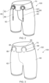
- Each conductive circuit 20a, 20b comprises four electrodes 22, 24, 26, 28 comprising areas of the circuit in which a conductive area of the circuit is arranged to contact the skin of a wearer.
- the electrodes 22, 24, 26, 28 are each electrically connected to a respective one of eight electrical contact points 30 by a respective conductive track 40.
- four of the electrical contact points 30 comprise part of the left conductive circuit 20a, and the remaining four electrical contact points 30 comprise part of the right conductive circuit 20b.
- each leg panel 60, 62 comprises a tab portion 68 that, when assembled into the shorts 100, extends into the waistband area.
- Each tab portion 68 carries the respective cluster of electrical contact points 30 for a respective one of the conductive circuits 20a, 20b.
- connection to the controller (not shown) via the connecting apparatus (described below) can be achieved in the waistband area, which has been found to be particularly comfortable for users.
- the tab portions 68 comprise a unitary part of each leg panel 60, 62, thereby avoiding the need for any seams crossing the conductive circuits 20a, 20b; seams have been found to adversely affect the electrical resistance of the circuit.
- the first pair of electrodes 22a, 22b are located in the region of a user's hip
- the second pair of electrodes 24a, 24b are located generally in the region of a user's upper anterior (front) thigh
- the third pair of electrodes 26a, 26b are located generally in the region of the user's buttock
- the fourth pair of electrodes 28a, 28b are located generally in the region of the user's upper posterior (rear) thigh.
- a visual line 90 is provided on each of the left and right leg panels 60, 62 to provide the user with a visual guide to help ensure correct location of the electrodes 22, 24, 26, 28.
- the visual line 90 should be aligned with the gluteal crease (also referred to as the gluteal sulcus or gluteal fold) that divides the buttocks from the posterior upper thigh.
- each of the electrodes has been found to be very important.
- the inventors have determined that it is especially important to carefully position the gluteal electrodes 26 relative to specific anatomical features. Through experimental analysis, they have established that one or more of (preferably all of) the following positional rules for each of the gluteal electrodes 26 should be adhered to in order to provide optimally effective therapy.
- the horizontal position of the gluteal electrodes 26 should be controlled as follows:
- each nearest side edge of each gluteal electrode is horizontally offset from a feature that aligns with the inter-gluteal cleft of a wearer in use by about between 12mm and 20mm, optionally about 17 or 18mm, e.g. about 17.5mm.
- a feature may comprise a line at the rear of the garment 100 bisecting left and right portions of the garment 100 (e.g. rear seam 64).
- the above positional rules can be satisfied by positioning the gluteal electrodes 26 on the garment 100 such that each uppermost edge thereof is vertically offset from a feature of the garment 100 that aligns with the user's natural waist in use by at least 70mm, optionally at least 75mm.
- each gluteal electrode 26 should be no more than 25mm above the point of hip.
- references to 'edges' in reference to these positional rules are references to edges of active regions of the respective electrode, i.e. edges of exposed regions in which the conductive material is exposed to contact the skin of a wearer during use.
- a particular benefit of the above positional rules is in ensuring correct placement of the gluteal electrodes 26 across multiple garment sizes.
- the conductive circuits 20a, 20b are each a mirror image of the other, but in other embodiments the layout of the conductive circuits 20a, 20b could be varied so that they differ from one another.
- the route and shape of the tracks 40 may be different on each leg panel 60, 62. In most embodiments it is expected that the position and shape of the left and right electrodes 22, 24, 26, 28 will be mirror images of one another.
- the tracks 40 have a generally wavy, or waveform, shape such that the path of each track generally zig-zags between the respective electrode 22, 24, 26, 28 and electrical contact 30.
- This arrangement has been found to be particularly beneficial because the waveform shape of the tracks 40 allows for the fabric of the leg panel 60, 62 to be stretched during use of the shorts 100 without unduly affecting the electrical resistance provided by the tracks 40. That is, the wavelength and/or amplitude of the waveform can vary to thereby minimise stretching of the one or more conductive layers of the track.
- the tracks have a generally linear shape.
- Each conductive circuit 20a, 20b is formed by printing of a series of conductive and non-conductive layers onto the fabric of the shorts (i.e. the fabric of each of the left and right leg panels 60, 62). An appropriate method of printing the conductive circuits 20a, 20b is described in GB2555592A .
- a series of layers is applied onto the fabric of the shorts to form each conductive circuit.
- the layers applied are an adhesive layer, an encapsulation layer (non-conductive layer), a layer of conductive ink (conductive layer, which may comprise first and second conductive layers), a further encapsulation layer (non-conductive layer).
- the further encapsulation layer is provided over areas of the conductive ink that should not be in contact with a user's skin, and leaves areas of exposed conductive ink, as conductive areas (electrodes).
- the further encapsulation layer comprises first and second non-conductive layers, as described further below.
- the conductive circuits 20a, 20b are generally formed by printing a series of conductive and non-conductive ink layers in a desired order onto a substrate (not shown), and then transferring the printed layers from the substrate onto the respective leg panel 60, 62 by a transfer process.
- the substrate may be placed over the leg panel 60, 62, heat and pressure applied to transfer the printed layers to the leg panel 60, 62, and the substrate subsequently peeled away.
- the printed layers may include an adhesive layer to facilitate bonding between the printed layers and the leg panel 60, 62.
- the layers may be printed directly onto the fabric of the leg panel 60, 62.
- the tracks 40 each comprise one or more layers of non-conductive material directly adjacent the fabric of the respective leg panel 60, 62, one or more layers of conductive material laminated over the one or more first layers of non-conductive material, and first and second layers of non-conductive material laminated over the one or more layers of conductive material.
- Each of the layers of non-conductive material is wider than the one or more layers of conductive material so that the layers of conductive material are encapsulated between the non-conductive layers.
- the one or more layers of conductive material can provide an electrical connection between the electrodes 22, 24, 26, 28 and the controller, via the connecting apparatus 80, while preventing any direct electrical connection between the tracks 40 and the skin of the user.
- the electrodes 22, 24, 26, 28 each comprise one or more layers of non-conductive material directly adjacent the fabric of the respective leg panel 60, 62, and one or more layers of conductive material laminated over the one or more layers of non-conductive material.
- the one or more layers of non-conductive material act to electrically isolate the layers of conductive material from the fabric. In this way, direct electrical connection between the electrodes 22, 24, 26, 28 and the skin of the user is possible by way of the direct contact between the user's skin and the conductive material only.
- By forming the electrodes with printed layers in this way stretching of the fabric in the region of each electrode is minimised, which is advantageous since this prevents undesirable increases in electrical resistance in the electrodes.
- First and second layers of non-conductive material are laminated around the peripheral edges of the layers of conductive material of each electrode only. This serves to both further prevent stretching of the fabric in the region of the electrodes, and to protect the peripheral edges of the layers of conductive material from damage by peeling or fretting.
- the one or more layers of conductive material of each electrode 22, 24, 26, 28 are contiguous with the one or more layers of conductive material of a respective one of the tracks 40 to thereby permit transfer of an electrical signal from the controller to each electrode 22, 24, 26, 28 via the one or more layers of conductive material.
- Figures 8A-C and 9A-C illustrate a conductive circuit 20 according to embodiments of the invention that are suitable for use in the shorts 100 of Figs. 1-7 .
- the circuit 20 illustrated is shown in a form 20a suitable for a left leg panel 30 of the shorts 100, but can equally be applied in mirror image to provide a form 20b suitable for a right leg panel 62 of the shorts 100.
- Figures 8A-C shows the outlines of the various layers within the circuit 20, while Figure 9A shows the visible extent of the layers at the skin-facing side of the circuit 20.
- the various layers are shown in cross-section in Figures 9B and 9C , although it is to be noted that these drawings are purely schematic in nature, not to scale, and not intended to provide a true representation of the geometry of the layers but instead an indication of their ordering and extent.
- the second encapsulating non-conductive layer 160 has a peripheral outline that corresponds generally to that of the first encapsulating non-conductive layer, with the exception that at the contacts 30 and at the interface 200 between each track 40 and its respective electrode 22, 24, 26, 28 the second encapsulating non-conductive layer 160 overhangs the first encapsulating non-conductive layer 170.
- the overhang provides an offset between a second perimeter edge of the second encapsulating non-conductive layer 160 and a first perimeter edge of the first encapsulating non-conductive layer 150 of about 1mm.
- Figures 8B and 9B illustrate the arrangement of layers in the conductive circuit 20 at each of the four (in the illustrated examples) contacts 30. Note that Figure 9B is schematic and not to scale. The skilled reader will understand that overhanging portions of layers will generally conform to the topography of the layers underneath, and will not remain straight and unyielding as illustrated.
- Each contact 30 comprises an exposed region of the one or more conductive layers 130, 140. In the illustrated examples it is the one or more track-only conductive layers 140 which are exposed, but in other embodiments any conductive layer may be exposed to form the contacts 30.
- each contact 30 is defined by a second perimeter edge of the second encapsulating non-conductive layer 160, the second perimeter edge forming a circle.
- the second perimeter edge is offset from a first perimeter edge of the first encapsulating non-conductive layer 150 so that the second encapsulating non-conductive layer 160 overhangs the first encapsulating non-conductive layer 150.
- the first perimeter edge thus also forms a circle that is concentric with the circle second perimeter edge, but having a larger diameter. In the illustrated examples the offset, or overhang, is approximately 1mm. This corresponds to more than 60 times a thickness of the first encapsulating non-conductive layer 150.
- Figures 8C and 9C illustrate the arrangement of layers in the conductive circuit around each of the four (in the illustrated examples) interfaces 200 between the tracks 40 and the electrodes 22, 24, 26, 28. Note that Figure 9C is schematic and not to scale. The skilled reader will understand that overhanging portions of layers will conform to the topography of the layers underneath, and will not remain straight and unyielding as illustrated.
- Each electrode 22, 24, 26, 28 comprises an exposed region of the one or more conductive layers 130, 140. In the illustrated examples it is the one or more track-and-electrode conductive layers 130 which are exposed, but in other examples any conductive layer may be exposed to form the electrodes 22, 24, 26, 28.
- the first and second encapsulating non-conductive layers 150, 160 terminate at first and second perimeter edges, respectively, adjacent to, but offset from, each interface 200 between track 40 and electrode 22, 24, 26, 28.
- the track-only conductive layer 140 (where present) also terminates at a perimeter edge adjacent to, but offset from, each interface 200.
- the perimeter edge of the track-only conductive layer 140 (where present) is coincident with the first perimeter edge of the first encapsulating non-conductive layer 150.
- Each of the first and second perimeter edges of the first and second encapsulating non-conductive layers 150, 160 and the perimeter edge of the track-only conductive layer 140 has a generally arcuate shape such that each layer comprises a generally semi-circular shaped projection 210 that extends from each track 40 beyond the interface 200 and over a portion of the respective electrode 22, 24, 26, 28 (i.e. over a portion of the track-and-electrode conductive layer 130 that is exposed to provide the respective electrode).
- the second perimeter edge of the second encapsulating non-conductive layer 160 is offset from the first perimeter edge of the first encapsulating non-conductive layer 150 such that the second encapsulating non-conductive layer 160 overhangs the first encapsulating non-conductive layer 150.
- the offset, or overhang is approximately 1mm. This corresponds to more than 60 times a thickness of the first encapsulating non-conductive layer 150.
- the interfaces 200 each comprise regions in which a relatively large cross-sectional area of printed layers in the electrode, where the modulus of elasticity is relatively high, meets a relatively small cross-sectional area of printed layers in the track, where the modulus of elasticity is relatively low. These regions can therefore comprise areas of weakness where high loads are concentrated.
- Figures 10A and 10B illustrate a further conductive circuit 20' according to embodiments of the invention that is applied to a left leg panel 60 suitable for making up the shorts 100 of Figs. 1-7 .
- the circuit 20' illustrated is shown in a form 20a suitable for a left leg panel 60 of the shorts 100, but can equally be applied in mirror image to provide a form 20b suitable for a right leg panel 62 of the shorts 100.
- the circuit 20' is formed by printing the plurality of printed layers, via any of the various processes described herein.
- Figure 10A shows the outlines of the various layers within the circuit 20', with the layers closest to the skin of a wearer shown uppermost in the figure.
- the outermost non-conductive layer 260 is shown in semi-transparent form throughout, and the hip electrode conductive layer 250 of the hip electrode 22 is also shown in semi-transparent form; this is purely to enable the path of the tracks 40 to be clearly seen.
- circuit 20' is formed from the following layers:
- a key difference between the conductive circuit 20' of Figures 10A and 10B and the conductive circuit 20 of Figures 8A-C and 9A-C is that in the conductive circuit 20' the layers of the tracks 40 pass between the hip electrode conductive layer(s) 250 of the hip electrode 22 and the base non-conductive layer(s) 220. That is, the hip electrode 22 overlies, or overlaps with, the tracks 40 that supply an electrical signal to the remaining three electrodes 24, 26, 28.
- the effect of overlapping the tracks 40 with the hip electrode 22 is achieved by electrically isolating the conductive layer(s) of the hip electrode 22 from the conductive layer(s) of the remaining electrodes 24, 26, 28 and the tracks 40 using the electrode isolating non-conductive layer 240.
- the hip electrode 22 is formed from a first conductive layer
- the remaining electrodes 24, 26, 28 and the tracks 40 are formed from a second conductive layer that is electrically isolated from the first conductive layer.
- Each contact 30 comprises an exposed region of conductive material.
- the contact 30 associated with the hip electrode 22 comprises an exposed region of the hip electrode conductive layer 250, and each of the remaining contacts 30 comprises an exposed region of the track-and-electrode conductive layer 230.
- each electrode 22, 24, 26, 28 comprises an exposed region of conductive material.
- each electrode 24, 26, 28 other than the hip electrode 22 comprises an exposed region of track-and-electrode conductive layer 230, and the hip electrode 22 comprises an exposed region of hip electrode conductive layer 250.
- the tracks 40 overlap with the hip electrode 22, but the skilled reader will understand that in other embodiments one or more of the tracks 40 may overlap with any electrode in a conductive circuit formed from a plurality of printed layers.
- the one or more layers of non-conductive material preferably comprise one or more non-conductive ink layers.
- a suitable printing ink comprises a water based printing ink, an ultraviolet-cured printing ink, a solvent based ink, or a latex printing ink, for example.
- a particularly preferred ink for the non-conductive layers comprises a screen-printable ink of CMYK toner.
- the one or more layers of conductive material preferably comprise one or more conductive ink layers.
- the conductive material may comprise an electrically conductive metal, such as silver, silver chloride, copper or combinations or alloys thereof, or another conductive material such as a carbon-containing material.
- Suitable conductive inks may be supplied by Engineering Materials Systems, Inc. under the brand name Engineered Conductive Materials (ECM)TM.
- Each of the layers of conductive or non-conductive material may have a thickness of 0.5mm or less, 0.4mm or less, 0.3mm or less, 0.2mm or less, 0.1mm or less, 0.05mm or less.
- each of the first and second layers of non-conductive material 150, 160 or the electrode isolating non-conductive layers 240 may be approximately 0.018mm thick.
- each of the layers of conductive material may be approximately 0.006mm thick.
- three layers of conductive material are provided in the tracks 40 and two layers are provided in the electrodes 22, 24, 26, 28.
- Each conductive circuit 20, 20a, 20b, 20' is provided with a connecting apparatus 80 to connect it to a controller (not shown).
- the controller may be as described in WO2007138071 .
- the connecting apparatus 80 may, for example, be a wire with appropriate connectors.
- the connecting apparatus 80 comprises left and right connectors 82 that provide an electrical connection between the conductive circuits 20, 20', 20a, 20b and left and right cables 86.
- Each connector 82 comprises a rigid two-part assembly.
- a first part of each connector 82 is durably fixed to a respective leg panel 60, 62 so that each of four electrical connecting pins within the first part form an electrical connection with a respective one of the four electrical contact points 30 of the respective conductive circuit 20, 20', 20a, 20b.
- a second part of each connector 82 can be removably connected to the first part to create an electrical connection therebetween.
- one or both of the first and second parts may comprise magnets to facilitate an easy interconnection.
- each connector 82 may comprise magnets with opposing polarities to ensure that a user connects the correct first and second parts together, and to prevent incorrect connection.
- the second part of each connector 82 provides a durable connection to the respective cable 86, which comprises a jack for connection of the shorts 100 with the controller (not shown).
- the fabric of the shorts 100 While it is desirable for the fabric of the shorts 100 to be stretchy to enable easy use by users and to ensure a good contact between the user's skin and the electrodes, it has been found that it is desirable to restrict stretch of the fabric in the region of the connectors 82 in order to ensure a reliable electrical connection between the controller and the conductive circuits 20, 20', 20a, 20b. In the illustrated embodiments this has been achieved by means of left and right rubber sheet layers 88 which are each sandwiched between the respective connector 82 and the fabric of the respective leg panel 60, 62. In preferred arrangements the rubber sheet layers 88 (and the fabric of the respective leg panel 60, 62) are each sandwiched between rigid portions of the first part of the respective connector 82. This arrangement not only provides a reliable electrical connection, but also serves to prevent water ingress into the connector 82, for example during washing of the shorts 100.
- Electrode connectivity between the electrodes 22, 24, 26, 28 and the user's skin is preferably maximised by use of an electrolytic fluid.
- the user may spray the electrodes with electrolytic solution or saline solution prior to use.
Landscapes
- Health & Medical Sciences (AREA)
- Life Sciences & Earth Sciences (AREA)
- Engineering & Computer Science (AREA)
- General Health & Medical Sciences (AREA)
- Veterinary Medicine (AREA)
- Biomedical Technology (AREA)
- Animal Behavior & Ethology (AREA)
- Public Health (AREA)
- Nuclear Medicine, Radiotherapy & Molecular Imaging (AREA)
- Radiology & Medical Imaging (AREA)
- Heart & Thoracic Surgery (AREA)
- Biophysics (AREA)
- Physics & Mathematics (AREA)
- Pathology (AREA)
- Medical Informatics (AREA)
- Molecular Biology (AREA)
- Surgery (AREA)
- Gastroenterology & Hepatology (AREA)
- Physiology (AREA)
- Cardiology (AREA)
- Rheumatology (AREA)
- Orthopedic Medicine & Surgery (AREA)
- Oral & Maxillofacial Surgery (AREA)
- Dentistry (AREA)
- Pulmonology (AREA)
- Physical Education & Sports Medicine (AREA)
- Textile Engineering (AREA)
- Biodiversity & Conservation Biology (AREA)
- Measurement And Recording Of Electrical Phenomena And Electrical Characteristics Of The Living Body (AREA)
- Electrotherapy Devices (AREA)
- Structure Of Printed Boards (AREA)
Claims (15)
- Circuit conducteur (20, 20a, 20b, 20') comprenant une ou plusieurs électrodes (22, 24, 26, 28) pour délivrer un signal électromagnétique à un corps humain ou animal, le circuit conducteur comprenant une base (60, 62) et une pluralité de couches imprimées (130, 140, 150, 160) supportées par la base (60, 62), la pluralité de couches imprimées (130, 140, 150, 160) comprenant une première couche imprimée non conductrice (150) au moins partiellement définie par un premier bord périphérique, et une seconde couche imprimée non conductrice (160) au moins partiellement définie par un second bord périphérique et recouvrant la première couche imprimée non conductrice (150), dans lequel au moins une partie du second bord périphérique est décalée par rapport au premier bord périphérique de telle sorte que la seconde couche imprimée non conductrice (160) surplombe la première couche imprimée non conductrice (150), une ou plusieurs pistes de connexion (40), chaque piste de connexion (40) fournissant un chemin électriquement conducteur entre l'une respective de l'une ou plusieurs électrodes (22, 24, 26, 28) et un contact électrique (30) configuré pour permettre la connexion à un contrôleur agencé pour fournir un signal électromagnétique à l'une ou plusieurs électrodes (22, 24, 26, 28), caractérisé en ce que le premier bord périphérique et/ou le second bord périphérique sont décalés d'une interface (200) entre chacune de l'une ou plusieurs pistes de connexion (40) et une respective de l'une ou plusieurs électrodes (22, 24, 26, 28).
- Circuit conducteur selon l'une quelconque des revendications précédentes, dans lequel la base (60, 62) comprend un tissu, éventuellement un tissu extensible (208).
- Circuit conducteur selon l'une quelconque des revendications précédentes, dans lequel les première et seconde couches imprimées non conductrices (150, 160) comportent un module d'élasticité plus élevé que la base (60, 62).
- Circuit conducteur selon l'une quelconque des revendications précédentes, dans lequel la pluralité de couches imprimées (130, 140, 150, 160) comprend une couche imprimée conductrice (130, 140) partiellement recouverte par les première et seconde couches imprimées non conductrices (150, 160), et le second bord périphérique définit une ou plusieurs régions exposées du circuit conducteur dans lesquelles la couche imprimée conductrice (130, 140) n'est pas recouverte par les première et seconde couches imprimées non conductrices (150, 160).
- Circuit conducteur selon l'une quelconque des revendications précédentes, dans lequel la seconde couche imprimée non conductrice (160) comprend une couche la plus externe du circuit conducteur.
- Circuit conducteur selon l'une quelconque des revendications précédentes, dans lequel la pluralité de couches imprimées comprend en outre au moins une couche imprimée conductrice (130, 140) supportée par la base (60, 62) et partiellement recouverte par les première et seconde couches imprimées non conductrices (150, 160) pour définir une ou plusieurs régions exposées de l'une ou plusieurs électrodes (22, 24, 26, 28) dans lesquelles l'au moins une couche imprimée conductrice (130, 140) est exposée pour être ainsi configurée pour entrer en contact avec la peau d'un corps humain ou animal en cours d'utilisation.
- Circuit conducteur selon l'une quelconque des revendications précédentes, dans lequel l'une ou plusieurs régions exposées de l'une ou plusieurs électrodes (22, 24, 26, 28) sont définies au moins partiellement par le second bord périphérique.
- Circuit conducteur selon l'une quelconque des revendications précédentes, dans lequel l'interface (200) entre chacune de l'une ou plusieurs pistes de connexion (40) et l'une respective de l'une ou plusieurs électrodes (22, 24, 26, 28) comprend une région dans laquelle une zone de section transversale du circuit conducteur change.
- Circuit conducteur selon l'une quelconque des revendications précédentes, dans lequel l'interface (200) entre chacune de l'une ou plusieurs pistes de connexion (40) et l'une respective de l'une ou plusieurs électrodes (22, 24, 26, 28) comprend une région dans laquelle un module d'élasticité du circuit conducteur change.
- Circuit conducteur selon l'une quelconque des revendications précédentes, dans lequel la pluralité de couches imprimées (130, 140, 150, 160) comprend une couche imprimée conductrice (130, 140) de l'une ou plusieurs pistes de connexion (40), la couche imprimée conductrice (130, 140) de chacune de l'une ou plusieurs pistes de connexion (40) étant électriquement connectée à l'une respective de l'une ou plusieurs électrodes (22, 24, 26, 28).
- Circuit conducteur selon la revendication 10, dans lequel la couche imprimée conductrice (130, 140) de chacune de l'une ou plusieurs pistes de connexion (40) est connectée électriquement à une couche imprimée conductrice (130, 140) de l'une respective de l'une ou plusieurs électrodes (22, 24, 26, 28).
- Circuit conducteur selon la revendication 10 ou la revendication 11, dans lequel les première et seconde couches imprimées non conductrices (150, 160) recouvrent la couche imprimée conductrice (130, 140) de chacune de l'une ou plusieurs pistes de connexion (40) pour ainsi encapsuler au moins une majorité de la couche imprimée conductrice (130, 140).
- Circuit conducteur selon la revendication 12, dans lequel le ou chaque contact électrique (30) comprend une région exposée de la piste de connexion respective (40) dans laquelle la couche imprimée conductrice (130, 140) de la piste de connexion (40) n'est pas recouverte par les première et seconde couches imprimées non conductrices (150, 160), et dans lequel la région exposée est définie par le second bord périphérique.
- Circuit conducteur selon l'une quelconque des revendications précédentes, comprenant un connecteur (82) connecté électriquement à l'un ou plusieurs contacts électriques (130, 140) et configuré pour fournir une connexion électrique entre l'une ou plusieurs électrodes (22, 24, 26, 28) et une alimentation, un contrôleur ou une unité de commande.
- Circuit conducteur selon l'une quelconque des revendications précédentes, dans lequel la pluralité de couches imprimées (130, 140, 150, 160) comprennent en outre une ou plusieurs couches imprimées non conductrices supplémentaires (120) entre une couche imprimée conductrice (130, 140) et la base (60, 62).
Applications Claiming Priority (4)
| Application Number | Priority Date | Filing Date | Title |
|---|---|---|---|
| GBGB1907520.9A GB201907520D0 (en) | 2019-05-28 | 2019-05-28 | Conductive circuit |
| GB1907517.5A GB2584626A (en) | 2019-05-28 | 2019-05-28 | Conductive circuit |
| GB1908771.7A GB2584879A (en) | 2019-06-19 | 2019-06-19 | Conductive circuit |
| PCT/EP2020/064912 WO2020239950A2 (fr) | 2019-05-28 | 2020-05-28 | Circuit conducteur |
Publications (2)
| Publication Number | Publication Date |
|---|---|
| EP3976166A2 EP3976166A2 (fr) | 2022-04-06 |
| EP3976166B1 true EP3976166B1 (fr) | 2023-12-13 |
Family
ID=71105440
Family Applications (1)
| Application Number | Title | Priority Date | Filing Date |
|---|---|---|---|
| EP20733530.8A Active EP3976166B1 (fr) | 2019-05-28 | 2020-05-28 | Circuit conducteur |
Country Status (6)
| Country | Link |
|---|---|
| US (2) | US12109406B2 (fr) |
| EP (1) | EP3976166B1 (fr) |
| JP (1) | JP2022534019A (fr) |
| CN (1) | CN114514050A (fr) |
| AU (1) | AU2020281922A1 (fr) |
| WO (1) | WO2020239950A2 (fr) |
Families Citing this family (5)
| Publication number | Priority date | Publication date | Assignee | Title |
|---|---|---|---|---|
| CN111787972B (zh) | 2017-12-04 | 2025-01-03 | 卡德拉医疗股份有限公司 | 导电电路 |
| WO2020239950A2 (fr) * | 2019-05-28 | 2020-12-03 | Atlantic Therapeutics Group Limited | Circuit conducteur |
| GB2602800B (en) * | 2021-01-13 | 2023-05-10 | Mygo4Ward Ltd | Improvements relating to functional electrical stimulation garments |
| EP4514443B1 (fr) * | 2022-04-29 | 2026-01-14 | Aarhus Universitet | Électrode à sec intégrée à un vêtement |
| WO2024197046A2 (fr) * | 2023-03-20 | 2024-09-26 | Motive Health, Inc. | Systèmes et procédés d'électrode et de vêtement pour une distribution améliorée de stimulation neuromusculaire |
Family Cites Families (44)
| Publication number | Priority date | Publication date | Assignee | Title |
|---|---|---|---|---|
| DE19730811C1 (de) * | 1997-07-18 | 1999-05-27 | Kendall Med Erzeugnisse Gmbh | Biomedizinische Elektrode und Verfahren zu deren Herstellung |
| JP2001057967A (ja) | 2000-01-01 | 2001-03-06 | Advance Co Ltd | 生体用電極の製造方法 |
| US20020099277A1 (en) * | 2000-09-12 | 2002-07-25 | Nexan Limited | Disposable vital signs monitoring sensor band with removable alignment sheet |
| US20020077688A1 (en) * | 2000-12-15 | 2002-06-20 | Kirkland Thomas C. | Electrode-positioning body garment |
| IES20010651A2 (en) | 2001-07-12 | 2003-01-22 | Bmr Res & Dev Ltd | A method and apparatus for applying electrical stimulation to a human or animal subject |
| US7077662B2 (en) * | 2002-01-15 | 2006-07-18 | Tribotek, Inc. | Contact woven connectors |
| JP2003250914A (ja) | 2002-03-05 | 2003-09-09 | Ya Man Ltd | トリートメント装置 |
| US20080077192A1 (en) | 2002-05-03 | 2008-03-27 | Afferent Corporation | System and method for neuro-stimulation |
| GB2438589A (en) | 2006-06-01 | 2007-12-05 | Bio Medical Res Ltd | Garment with integrated electrodes and data storage for parameters related to measurement or stimulation of the wearers body |
| US7504550B2 (en) | 2006-08-31 | 2009-03-17 | Kimberly-Clark Worldwide, Inc. | Conductive porous materials |
| JP5186506B2 (ja) | 2007-09-25 | 2013-04-17 | 朝倉染布株式会社 | 電極シート及び電極シートの製造方法 |
| JP5661648B2 (ja) | 2009-01-26 | 2015-01-28 | ユニバーシティ・カレッジ・ダブリン,ナショナル・ユニバーシティ・オブ・アイルランド,ダブリン | 骨盤底筋を刺激する方法及び装置 |
| JP2010220754A (ja) | 2009-03-23 | 2010-10-07 | Alcare Co Ltd | 電気治療器 |
| JP2011018873A (ja) * | 2009-05-22 | 2011-01-27 | Sony Ericsson Mobilecommunications Japan Inc | 電磁シールド方法および電磁シールド用フィルム |
| EP2451525B1 (fr) | 2009-07-10 | 2019-06-12 | University College Dublin National University Of Ireland, Dublin | Appareil de stimulation des muscles du bas du dos et abdominaux |
| US8560040B2 (en) | 2010-01-04 | 2013-10-15 | Koninklijke Philips N.V. | Shielded biomedical electrode patch |
| AT510914B1 (de) * | 2011-01-03 | 2012-10-15 | Lang Leonh | Medizinische elektrode mit gedruckter zuleitung und verfahren zu ihrer herstellung |
| JP6212395B2 (ja) | 2011-03-02 | 2017-10-11 | マードック チルドレンズ リサーチ インスティテュート | 経皮的刺激システム |
| CN107456653B (zh) * | 2011-07-18 | 2021-06-22 | Empi有限公司 | 电极、电极系统和制造方法以及离子电渗递送系统 |
| US9386684B2 (en) * | 2012-03-20 | 2016-07-05 | Molex, Llc | Physical contact layer for body-worn leadware using selective deposition |
| US20150366504A1 (en) * | 2014-06-20 | 2015-12-24 | Medibotics Llc | Electromyographic Clothing |
| US10462898B2 (en) | 2012-09-11 | 2019-10-29 | L.I.F.E. Corporation S.A. | Physiological monitoring garments |
| US8948839B1 (en) | 2013-08-06 | 2015-02-03 | L.I.F.E. Corporation S.A. | Compression garments having stretchable and conductive ink |
| CA2938025C (fr) | 2014-01-28 | 2021-11-16 | Nippon Telegraph And Telephone Corporation | Vetement detecteur de biosignal |
| US10035016B2 (en) | 2014-04-14 | 2018-07-31 | Elidah, Inc. | Electrical stimulation device |
| EP3191171B1 (fr) * | 2014-09-10 | 2022-12-14 | Ecole Polytechnique Fédérale de Lausanne (EPFL) | Électrode pouvant être dessinée non-effractive pour stimulation électrique neuromusculaire et détection de signal biologique |
| CA3313317A1 (en) | 2015-11-02 | 2026-06-21 | Honeywell Safety Products Usa, Inc. | Biosensing garment |
| US11147719B2 (en) * | 2015-11-16 | 2021-10-19 | Hill-Rom Services, Inc. | Incontinence detection systems for hospital beds |
| US10231623B2 (en) * | 2016-02-04 | 2019-03-19 | Nanowear Inc. | Roll-to-roll printing process for manufacturing a wireless nanosensor |
| CN109890453A (zh) | 2016-09-26 | 2019-06-14 | 生物医药研究有限公司 | 用于经皮刺激电极的电解质衬里 |
| US10386224B2 (en) * | 2016-10-25 | 2019-08-20 | Studio 1 Labs Inc. | Flexible conductive apparatus and systems for detecting pressure |
| GB2555592B (en) * | 2016-11-02 | 2019-02-27 | Conductive Transfers Ltd | Transfer for application to a surface |
| CN110381826A (zh) | 2016-11-25 | 2019-10-25 | 约翰·丹尼尔斯 | 人机触觉界面和可穿戴电子产品方法及装置 |
| FI20175818A1 (en) * | 2017-09-14 | 2019-03-15 | Clothing Plus Mbu Oy | Electrical signal transmission system |
| USD864523S1 (en) | 2017-11-13 | 2019-10-29 | Craig H. Diamond | Supportive garment |
| CN111787972B (zh) | 2017-12-04 | 2025-01-03 | 卡德拉医疗股份有限公司 | 导电电路 |
| USD847457S1 (en) | 2018-04-23 | 2019-05-07 | Bsn Sports, Llc | Pads set for a girdle |
| US12114715B2 (en) | 2018-10-23 | 2024-10-15 | Clearview Systems, Llc | Athletic garment |
| USD917127S1 (en) | 2019-02-11 | 2021-04-27 | Clinton Chisholm | Double-lined interior and exterior pocket male undergarment |
| WO2020239950A2 (fr) | 2019-05-28 | 2020-12-03 | Atlantic Therapeutics Group Limited | Circuit conducteur |
| WO2021067658A1 (fr) | 2019-10-03 | 2021-04-08 | Primetime Ventures, LLC | Vêtement pour homme pour la récupération après des procédures urologiques, une chirurgie génitale et une lésion génitale |
| USD922730S1 (en) | 2019-11-15 | 2021-06-22 | Edward Bae | Underwear with small inside right pocket |
| USD939189S1 (en) | 2020-10-20 | 2021-12-28 | Oona De Mulder | Exercise shorts |
| USD953694S1 (en) | 2020-12-11 | 2022-06-07 | zhengzhouaozhilaishangmaoyouxiangongsi | Men's underwear |
-
2020
- 2020-05-28 WO PCT/EP2020/064912 patent/WO2020239950A2/fr not_active Ceased
- 2020-05-28 US US17/614,122 patent/US12109406B2/en active Active
- 2020-05-28 AU AU2020281922A patent/AU2020281922A1/en not_active Abandoned
- 2020-05-28 JP JP2021569245A patent/JP2022534019A/ja active Pending
- 2020-05-28 EP EP20733530.8A patent/EP3976166B1/fr active Active
- 2020-05-28 CN CN202080048859.3A patent/CN114514050A/zh active Pending
-
2024
- 2024-08-29 US US18/820,052 patent/US20240424287A1/en active Pending
Also Published As
| Publication number | Publication date |
|---|---|
| WO2020239950A3 (fr) | 2021-01-07 |
| US20240424287A1 (en) | 2024-12-26 |
| US12109406B2 (en) | 2024-10-08 |
| US20220152380A1 (en) | 2022-05-19 |
| JP2022534019A (ja) | 2022-07-27 |
| WO2020239950A2 (fr) | 2020-12-03 |
| CN114514050A (zh) | 2022-05-17 |
| EP3976166A2 (fr) | 2022-04-06 |
| AU2020281922A1 (en) | 2022-01-20 |
Similar Documents
| Publication | Publication Date | Title |
|---|---|---|
| US20240108879A1 (en) | Conductive Circuit | |
| US20240424287A1 (en) | Conductive Circuit | |
| CA2749828C (fr) | Procede et appareil de stimulation des muscles du plancher pelvien | |
| EP2165733B1 (fr) | Vêtement conçu pour stimuler électriquement des muscles | |
| US8092273B2 (en) | Underwear for lower parts | |
| US20200188652A1 (en) | System and device for transcutaneous electrical nerve stimulation | |
| EP3967115B1 (fr) | Transfert conducteur et procédé de fabrication de celui-ci | |
| WO2024079332A1 (fr) | Mise au point de circuit d'encre d'imprimerie | |
| GB2584879A (en) | Conductive circuit | |
| GB2584626A (en) | Conductive circuit | |
| JP2003293203A (ja) | 陸上競技用スパッツ | |
| CN201529320U (zh) | 导电硅胶按摩器 | |
| US20220176121A1 (en) | Addressable electrode array systems, devices and methods | |
| CA3189503A1 (fr) | Vetements pour stimulation electrique | |
| CN222517564U (zh) | 一种多功能能量短裤 | |
| JP2000237332A (ja) | パルス美容器 | |
| KR20200060016A (ko) | 전기자극을 이용한 다이어트용 웨어 | |
| CN221998646U (zh) | 可穿戴理疗服装 | |
| ES2774721T3 (es) | Aparato para la estimulación de los músculos del suelo pélvico |
Legal Events
| Date | Code | Title | Description |
|---|---|---|---|
| STAA | Information on the status of an ep patent application or granted ep patent |
Free format text: STATUS: UNKNOWN |
|
| STAA | Information on the status of an ep patent application or granted ep patent |
Free format text: STATUS: THE INTERNATIONAL PUBLICATION HAS BEEN MADE |
|
| PUAI | Public reference made under article 153(3) epc to a published international application that has entered the european phase |
Free format text: ORIGINAL CODE: 0009012 |
|
| STAA | Information on the status of an ep patent application or granted ep patent |
Free format text: STATUS: REQUEST FOR EXAMINATION WAS MADE |
|
| 17P | Request for examination filed |
Effective date: 20211221 |
|
| AK | Designated contracting states |
Kind code of ref document: A2 Designated state(s): AL AT BE BG CH CY CZ DE DK EE ES FI FR GB GR HR HU IE IS IT LI LT LU LV MC MK MT NL NO PL PT RO RS SE SI SK SM TR |
|
| DAV | Request for validation of the european patent (deleted) | ||
| DAX | Request for extension of the european patent (deleted) | ||
| GRAP | Despatch of communication of intention to grant a patent |
Free format text: ORIGINAL CODE: EPIDOSNIGR1 |
|
| STAA | Information on the status of an ep patent application or granted ep patent |
Free format text: STATUS: GRANT OF PATENT IS INTENDED |
|
| INTG | Intention to grant announced |
Effective date: 20230628 |
|
| GRAS | Grant fee paid |
Free format text: ORIGINAL CODE: EPIDOSNIGR3 |
|
| GRAA | (expected) grant |
Free format text: ORIGINAL CODE: 0009210 |
|
| STAA | Information on the status of an ep patent application or granted ep patent |
Free format text: STATUS: THE PATENT HAS BEEN GRANTED |
|
| RAP1 | Party data changed (applicant data changed or rights of an application transferred) |
Owner name: CARBALLO LIMITED |
|
| AK | Designated contracting states |
Kind code of ref document: B1 Designated state(s): AL AT BE BG CH CY CZ DE DK EE ES FI FR GB GR HR HU IE IS IT LI LT LU LV MC MK MT NL NO PL PT RO RS SE SI SK SM TR |
|
| P01 | Opt-out of the competence of the unified patent court (upc) registered |
Effective date: 20231107 |
|
| REG | Reference to a national code |
Ref country code: GB Ref legal event code: FG4D |
|
| REG | Reference to a national code |
Ref country code: CH Ref legal event code: EP |
|
| REG | Reference to a national code |
Ref country code: DE Ref legal event code: R096 Ref document number: 602020022704 Country of ref document: DE |
|
| REG | Reference to a national code |
Ref country code: IE Ref legal event code: FG4D |
|
| PG25 | Lapsed in a contracting state [announced via postgrant information from national office to epo] |
Ref country code: GR Free format text: LAPSE BECAUSE OF FAILURE TO SUBMIT A TRANSLATION OF THE DESCRIPTION OR TO PAY THE FEE WITHIN THE PRESCRIBED TIME-LIMIT Effective date: 20240314 |
|
| REG | Reference to a national code |
Ref country code: LT Ref legal event code: MG9D |
|
| PG25 | Lapsed in a contracting state [announced via postgrant information from national office to epo] |
Ref country code: LT Free format text: LAPSE BECAUSE OF FAILURE TO SUBMIT A TRANSLATION OF THE DESCRIPTION OR TO PAY THE FEE WITHIN THE PRESCRIBED TIME-LIMIT Effective date: 20231213 |
|
| REG | Reference to a national code |
Ref country code: NL Ref legal event code: MP Effective date: 20231213 |
|
| PG25 | Lapsed in a contracting state [announced via postgrant information from national office to epo] |
Ref country code: ES Free format text: LAPSE BECAUSE OF FAILURE TO SUBMIT A TRANSLATION OF THE DESCRIPTION OR TO PAY THE FEE WITHIN THE PRESCRIBED TIME-LIMIT Effective date: 20231213 |
|
| PG25 | Lapsed in a contracting state [announced via postgrant information from national office to epo] |
Ref country code: LT Free format text: LAPSE BECAUSE OF FAILURE TO SUBMIT A TRANSLATION OF THE DESCRIPTION OR TO PAY THE FEE WITHIN THE PRESCRIBED TIME-LIMIT Effective date: 20231213 Ref country code: GR Free format text: LAPSE BECAUSE OF FAILURE TO SUBMIT A TRANSLATION OF THE DESCRIPTION OR TO PAY THE FEE WITHIN THE PRESCRIBED TIME-LIMIT Effective date: 20240314 Ref country code: ES Free format text: LAPSE BECAUSE OF FAILURE TO SUBMIT A TRANSLATION OF THE DESCRIPTION OR TO PAY THE FEE WITHIN THE PRESCRIBED TIME-LIMIT Effective date: 20231213 Ref country code: BG Free format text: LAPSE BECAUSE OF FAILURE TO SUBMIT A TRANSLATION OF THE DESCRIPTION OR TO PAY THE FEE WITHIN THE PRESCRIBED TIME-LIMIT Effective date: 20240313 |
|
| REG | Reference to a national code |
Ref country code: AT Ref legal event code: MK05 Ref document number: 1639971 Country of ref document: AT Kind code of ref document: T Effective date: 20231213 |
|
| PG25 | Lapsed in a contracting state [announced via postgrant information from national office to epo] |
Ref country code: NL Free format text: LAPSE BECAUSE OF FAILURE TO SUBMIT A TRANSLATION OF THE DESCRIPTION OR TO PAY THE FEE WITHIN THE PRESCRIBED TIME-LIMIT Effective date: 20231213 |
|
| PG25 | Lapsed in a contracting state [announced via postgrant information from national office to epo] |
Ref country code: SE Free format text: LAPSE BECAUSE OF FAILURE TO SUBMIT A TRANSLATION OF THE DESCRIPTION OR TO PAY THE FEE WITHIN THE PRESCRIBED TIME-LIMIT Effective date: 20231213 Ref country code: RS Free format text: LAPSE BECAUSE OF FAILURE TO SUBMIT A TRANSLATION OF THE DESCRIPTION OR TO PAY THE FEE WITHIN THE PRESCRIBED TIME-LIMIT Effective date: 20231213 Ref country code: NO Free format text: LAPSE BECAUSE OF FAILURE TO SUBMIT A TRANSLATION OF THE DESCRIPTION OR TO PAY THE FEE WITHIN THE PRESCRIBED TIME-LIMIT Effective date: 20240313 Ref country code: NL Free format text: LAPSE BECAUSE OF FAILURE TO SUBMIT A TRANSLATION OF THE DESCRIPTION OR TO PAY THE FEE WITHIN THE PRESCRIBED TIME-LIMIT Effective date: 20231213 Ref country code: LV Free format text: LAPSE BECAUSE OF FAILURE TO SUBMIT A TRANSLATION OF THE DESCRIPTION OR TO PAY THE FEE WITHIN THE PRESCRIBED TIME-LIMIT Effective date: 20231213 Ref country code: HR Free format text: LAPSE BECAUSE OF FAILURE TO SUBMIT A TRANSLATION OF THE DESCRIPTION OR TO PAY THE FEE WITHIN THE PRESCRIBED TIME-LIMIT Effective date: 20231213 |
|
| PG25 | Lapsed in a contracting state [announced via postgrant information from national office to epo] |
Ref country code: IS Free format text: LAPSE BECAUSE OF FAILURE TO SUBMIT A TRANSLATION OF THE DESCRIPTION OR TO PAY THE FEE WITHIN THE PRESCRIBED TIME-LIMIT Effective date: 20240413 |
|
| PG25 | Lapsed in a contracting state [announced via postgrant information from national office to epo] |
Ref country code: AT Free format text: LAPSE BECAUSE OF FAILURE TO SUBMIT A TRANSLATION OF THE DESCRIPTION OR TO PAY THE FEE WITHIN THE PRESCRIBED TIME-LIMIT Effective date: 20231213 Ref country code: CZ Free format text: LAPSE BECAUSE OF FAILURE TO SUBMIT A TRANSLATION OF THE DESCRIPTION OR TO PAY THE FEE WITHIN THE PRESCRIBED TIME-LIMIT Effective date: 20231213 |
|
| PG25 | Lapsed in a contracting state [announced via postgrant information from national office to epo] |
Ref country code: SK Free format text: LAPSE BECAUSE OF FAILURE TO SUBMIT A TRANSLATION OF THE DESCRIPTION OR TO PAY THE FEE WITHIN THE PRESCRIBED TIME-LIMIT Effective date: 20231213 |
|
| PG25 | Lapsed in a contracting state [announced via postgrant information from national office to epo] |
Ref country code: SM Free format text: LAPSE BECAUSE OF FAILURE TO SUBMIT A TRANSLATION OF THE DESCRIPTION OR TO PAY THE FEE WITHIN THE PRESCRIBED TIME-LIMIT Effective date: 20231213 Ref country code: SK Free format text: LAPSE BECAUSE OF FAILURE TO SUBMIT A TRANSLATION OF THE DESCRIPTION OR TO PAY THE FEE WITHIN THE PRESCRIBED TIME-LIMIT Effective date: 20231213 Ref country code: RO Free format text: LAPSE BECAUSE OF FAILURE TO SUBMIT A TRANSLATION OF THE DESCRIPTION OR TO PAY THE FEE WITHIN THE PRESCRIBED TIME-LIMIT Effective date: 20231213 Ref country code: IT Free format text: LAPSE BECAUSE OF FAILURE TO SUBMIT A TRANSLATION OF THE DESCRIPTION OR TO PAY THE FEE WITHIN THE PRESCRIBED TIME-LIMIT Effective date: 20231213 Ref country code: IS Free format text: LAPSE BECAUSE OF FAILURE TO SUBMIT A TRANSLATION OF THE DESCRIPTION OR TO PAY THE FEE WITHIN THE PRESCRIBED TIME-LIMIT Effective date: 20240413 Ref country code: EE Free format text: LAPSE BECAUSE OF FAILURE TO SUBMIT A TRANSLATION OF THE DESCRIPTION OR TO PAY THE FEE WITHIN THE PRESCRIBED TIME-LIMIT Effective date: 20231213 Ref country code: CZ Free format text: LAPSE BECAUSE OF FAILURE TO SUBMIT A TRANSLATION OF THE DESCRIPTION OR TO PAY THE FEE WITHIN THE PRESCRIBED TIME-LIMIT Effective date: 20231213 Ref country code: AT Free format text: LAPSE BECAUSE OF FAILURE TO SUBMIT A TRANSLATION OF THE DESCRIPTION OR TO PAY THE FEE WITHIN THE PRESCRIBED TIME-LIMIT Effective date: 20231213 |
|
| PG25 | Lapsed in a contracting state [announced via postgrant information from national office to epo] |
Ref country code: PT Free format text: LAPSE BECAUSE OF FAILURE TO SUBMIT A TRANSLATION OF THE DESCRIPTION OR TO PAY THE FEE WITHIN THE PRESCRIBED TIME-LIMIT Effective date: 20240415 Ref country code: PL Free format text: LAPSE BECAUSE OF FAILURE TO SUBMIT A TRANSLATION OF THE DESCRIPTION OR TO PAY THE FEE WITHIN THE PRESCRIBED TIME-LIMIT Effective date: 20231213 |
|
| PG25 | Lapsed in a contracting state [announced via postgrant information from national office to epo] |
Ref country code: PT Free format text: LAPSE BECAUSE OF FAILURE TO SUBMIT A TRANSLATION OF THE DESCRIPTION OR TO PAY THE FEE WITHIN THE PRESCRIBED TIME-LIMIT Effective date: 20240415 Ref country code: PL Free format text: LAPSE BECAUSE OF FAILURE TO SUBMIT A TRANSLATION OF THE DESCRIPTION OR TO PAY THE FEE WITHIN THE PRESCRIBED TIME-LIMIT Effective date: 20231213 |
|
| REG | Reference to a national code |
Ref country code: DE Ref legal event code: R097 Ref document number: 602020022704 Country of ref document: DE |
|
| PG25 | Lapsed in a contracting state [announced via postgrant information from national office to epo] |
Ref country code: DK Free format text: LAPSE BECAUSE OF FAILURE TO SUBMIT A TRANSLATION OF THE DESCRIPTION OR TO PAY THE FEE WITHIN THE PRESCRIBED TIME-LIMIT Effective date: 20231213 |
|
| PLBE | No opposition filed within time limit |
Free format text: ORIGINAL CODE: 0009261 |
|
| STAA | Information on the status of an ep patent application or granted ep patent |
Free format text: STATUS: NO OPPOSITION FILED WITHIN TIME LIMIT |
|
| PG25 | Lapsed in a contracting state [announced via postgrant information from national office to epo] |
Ref country code: SI Free format text: LAPSE BECAUSE OF FAILURE TO SUBMIT A TRANSLATION OF THE DESCRIPTION OR TO PAY THE FEE WITHIN THE PRESCRIBED TIME-LIMIT Effective date: 20231213 |
|
| PG25 | Lapsed in a contracting state [announced via postgrant information from national office to epo] |
Ref country code: SI Free format text: LAPSE BECAUSE OF FAILURE TO SUBMIT A TRANSLATION OF THE DESCRIPTION OR TO PAY THE FEE WITHIN THE PRESCRIBED TIME-LIMIT Effective date: 20231213 Ref country code: DK Free format text: LAPSE BECAUSE OF FAILURE TO SUBMIT A TRANSLATION OF THE DESCRIPTION OR TO PAY THE FEE WITHIN THE PRESCRIBED TIME-LIMIT Effective date: 20231213 |
|
| 26N | No opposition filed |
Effective date: 20240916 |
|
| REG | Reference to a national code |
Ref country code: CH Ref legal event code: PL |
|
| PG25 | Lapsed in a contracting state [announced via postgrant information from national office to epo] |
Ref country code: MC Free format text: LAPSE BECAUSE OF FAILURE TO SUBMIT A TRANSLATION OF THE DESCRIPTION OR TO PAY THE FEE WITHIN THE PRESCRIBED TIME-LIMIT Effective date: 20231213 |
|
| PG25 | Lapsed in a contracting state [announced via postgrant information from national office to epo] |
Ref country code: LU Free format text: LAPSE BECAUSE OF NON-PAYMENT OF DUE FEES Effective date: 20240528 |
|
| PG25 | Lapsed in a contracting state [announced via postgrant information from national office to epo] |
Ref country code: MC Free format text: LAPSE BECAUSE OF FAILURE TO SUBMIT A TRANSLATION OF THE DESCRIPTION OR TO PAY THE FEE WITHIN THE PRESCRIBED TIME-LIMIT Effective date: 20231213 Ref country code: LU Free format text: LAPSE BECAUSE OF NON-PAYMENT OF DUE FEES Effective date: 20240528 Ref country code: CH Free format text: LAPSE BECAUSE OF NON-PAYMENT OF DUE FEES Effective date: 20240531 |
|
| REG | Reference to a national code |
Ref country code: BE Ref legal event code: MM Effective date: 20240531 |
|
| PG25 | Lapsed in a contracting state [announced via postgrant information from national office to epo] |
Ref country code: IE Free format text: LAPSE BECAUSE OF NON-PAYMENT OF DUE FEES Effective date: 20240528 |
|
| PG25 | Lapsed in a contracting state [announced via postgrant information from national office to epo] |
Ref country code: BE Free format text: LAPSE BECAUSE OF NON-PAYMENT OF DUE FEES Effective date: 20240531 |
|
| PGFP | Annual fee paid to national office [announced via postgrant information from national office to epo] |
Ref country code: DE Payment date: 20250618 Year of fee payment: 6 |
|
| PGFP | Annual fee paid to national office [announced via postgrant information from national office to epo] |
Ref country code: GB Payment date: 20250618 Year of fee payment: 6 |
|
| PGFP | Annual fee paid to national office [announced via postgrant information from national office to epo] |
Ref country code: FR Payment date: 20250530 Year of fee payment: 6 |
|
| PG25 | Lapsed in a contracting state [announced via postgrant information from national office to epo] |
Ref country code: CY Free format text: LAPSE BECAUSE OF FAILURE TO SUBMIT A TRANSLATION OF THE DESCRIPTION OR TO PAY THE FEE WITHIN THE PRESCRIBED TIME-LIMIT; INVALID AB INITIO Effective date: 20200528 |
|
| PG25 | Lapsed in a contracting state [announced via postgrant information from national office to epo] |
Ref country code: FI Free format text: LAPSE BECAUSE OF FAILURE TO SUBMIT A TRANSLATION OF THE DESCRIPTION OR TO PAY THE FEE WITHIN THE PRESCRIBED TIME-LIMIT Effective date: 20231213 |
|
| PG25 | Lapsed in a contracting state [announced via postgrant information from national office to epo] |
Ref country code: HU Free format text: LAPSE BECAUSE OF FAILURE TO SUBMIT A TRANSLATION OF THE DESCRIPTION OR TO PAY THE FEE WITHIN THE PRESCRIBED TIME-LIMIT; INVALID AB INITIO Effective date: 20200528 |
|
| PG25 | Lapsed in a contracting state [announced via postgrant information from national office to epo] |
Ref country code: TR Free format text: LAPSE BECAUSE OF FAILURE TO SUBMIT A TRANSLATION OF THE DESCRIPTION OR TO PAY THE FEE WITHIN THE PRESCRIBED TIME-LIMIT Effective date: 20231213 |