EP3975241A1 - Method for manufacturing wiring board - Google Patents
Method for manufacturing wiring board Download PDFInfo
- Publication number
- EP3975241A1 EP3975241A1 EP20810059.4A EP20810059A EP3975241A1 EP 3975241 A1 EP3975241 A1 EP 3975241A1 EP 20810059 A EP20810059 A EP 20810059A EP 3975241 A1 EP3975241 A1 EP 3975241A1
- Authority
- EP
- European Patent Office
- Prior art keywords
- circuit board
- resin
- board component
- support
- interposer
- Prior art date
- Legal status (The legal status is an assumption and is not a legal conclusion. Google has not performed a legal analysis and makes no representation as to the accuracy of the status listed.)
- Granted
Links
Images




Classifications
-
- H—ELECTRICITY
- H10—SEMICONDUCTOR DEVICES; ELECTRIC SOLID-STATE DEVICES NOT OTHERWISE PROVIDED FOR
- H10P—GENERIC PROCESSES OR APPARATUS FOR THE MANUFACTURE OR TREATMENT OF DEVICES COVERED BY CLASS H10
- H10P72/00—Handling or holding of wafers, substrates or devices during manufacture or treatment thereof
- H10P72/70—Handling or holding of wafers, substrates or devices during manufacture or treatment thereof for supporting or gripping
- H10P72/74—Handling or holding of wafers, substrates or devices during manufacture or treatment thereof for supporting or gripping using temporarily an auxiliary support
-
- H—ELECTRICITY
- H05—ELECTRIC TECHNIQUES NOT OTHERWISE PROVIDED FOR
- H05K—PRINTED CIRCUITS; CASINGS OR CONSTRUCTIONAL DETAILS OF ELECTRIC APPARATUS; MANUFACTURE OF ASSEMBLAGES OF ELECTRICAL COMPONENTS
- H05K3/00—Apparatus or processes for manufacturing printed circuits
- H05K3/46—Manufacturing multilayer circuits
-
- H—ELECTRICITY
- H05—ELECTRIC TECHNIQUES NOT OTHERWISE PROVIDED FOR
- H05K—PRINTED CIRCUITS; CASINGS OR CONSTRUCTIONAL DETAILS OF ELECTRIC APPARATUS; MANUFACTURE OF ASSEMBLAGES OF ELECTRICAL COMPONENTS
- H05K1/00—Printed circuits
- H05K1/02—Details
- H05K1/14—Structural association of two or more printed circuits
-
- H—ELECTRICITY
- H05—ELECTRIC TECHNIQUES NOT OTHERWISE PROVIDED FOR
- H05K—PRINTED CIRCUITS; CASINGS OR CONSTRUCTIONAL DETAILS OF ELECTRIC APPARATUS; MANUFACTURE OF ASSEMBLAGES OF ELECTRICAL COMPONENTS
- H05K3/00—Apparatus or processes for manufacturing printed circuits
- H05K3/22—Secondary treatment of printed circuits
- H05K3/28—Applying non-metallic protective coatings
- H05K3/284—Applying non-metallic protective coatings for encapsulating mounted components
-
- H—ELECTRICITY
- H05—ELECTRIC TECHNIQUES NOT OTHERWISE PROVIDED FOR
- H05K—PRINTED CIRCUITS; CASINGS OR CONSTRUCTIONAL DETAILS OF ELECTRIC APPARATUS; MANUFACTURE OF ASSEMBLAGES OF ELECTRICAL COMPONENTS
- H05K3/00—Apparatus or processes for manufacturing printed circuits
- H05K3/30—Assembling printed circuits with electric components, e.g. with resistors
- H05K3/303—Assembling printed circuits with electric components, e.g. with resistors with surface mounted components
- H05K3/305—Affixing by adhesive
-
- H—ELECTRICITY
- H05—ELECTRIC TECHNIQUES NOT OTHERWISE PROVIDED FOR
- H05K—PRINTED CIRCUITS; CASINGS OR CONSTRUCTIONAL DETAILS OF ELECTRIC APPARATUS; MANUFACTURE OF ASSEMBLAGES OF ELECTRICAL COMPONENTS
- H05K3/00—Apparatus or processes for manufacturing printed circuits
- H05K3/30—Assembling printed circuits with electric components, e.g. with resistors
- H05K3/32—Assembling printed circuits with electric components, e.g. with resistors electrically connecting electric components or wires to printed circuits
- H05K3/34—Assembling printed circuits with electric components, e.g. with resistors electrically connecting electric components or wires to printed circuits by soldering
- H05K3/341—Surface mounted components
- H05K3/3431—Leadless components
- H05K3/3436—Leadless components having an array of bottom contacts, e.g. pad grid array or ball grid array components
-
- H—ELECTRICITY
- H05—ELECTRIC TECHNIQUES NOT OTHERWISE PROVIDED FOR
- H05K—PRINTED CIRCUITS; CASINGS OR CONSTRUCTIONAL DETAILS OF ELECTRIC APPARATUS; MANUFACTURE OF ASSEMBLAGES OF ELECTRICAL COMPONENTS
- H05K3/00—Apparatus or processes for manufacturing printed circuits
- H05K3/36—Assembling printed circuits with other printed circuits
-
- H—ELECTRICITY
- H10—SEMICONDUCTOR DEVICES; ELECTRIC SOLID-STATE DEVICES NOT OTHERWISE PROVIDED FOR
- H10W—GENERIC PACKAGES, INTERCONNECTIONS, CONNECTORS OR OTHER CONSTRUCTIONAL DETAILS OF DEVICES COVERED BY CLASS H10
- H10W70/00—Package substrates; Interposers; Redistribution layers [RDL]
- H10W70/01—Manufacture or treatment
- H10W70/05—Manufacture or treatment of insulating or insulated package substrates, or of interposers, or of redistribution layers
-
- H—ELECTRICITY
- H10—SEMICONDUCTOR DEVICES; ELECTRIC SOLID-STATE DEVICES NOT OTHERWISE PROVIDED FOR
- H10W—GENERIC PACKAGES, INTERCONNECTIONS, CONNECTORS OR OTHER CONSTRUCTIONAL DETAILS OF DEVICES COVERED BY CLASS H10
- H10W70/00—Package substrates; Interposers; Redistribution layers [RDL]
- H10W70/01—Manufacture or treatment
- H10W70/05—Manufacture or treatment of insulating or insulated package substrates, or of interposers, or of redistribution layers
- H10W70/093—Connecting or disconnecting other interconnections thereto or therefrom, e.g. connecting bond wires or bumps
-
- H—ELECTRICITY
- H10—SEMICONDUCTOR DEVICES; ELECTRIC SOLID-STATE DEVICES NOT OTHERWISE PROVIDED FOR
- H10W—GENERIC PACKAGES, INTERCONNECTIONS, CONNECTORS OR OTHER CONSTRUCTIONAL DETAILS OF DEVICES COVERED BY CLASS H10
- H10W70/00—Package substrates; Interposers; Redistribution layers [RDL]
- H10W70/01—Manufacture or treatment
- H10W70/05—Manufacture or treatment of insulating or insulated package substrates, or of interposers, or of redistribution layers
- H10W70/097—Cleaning
-
- H—ELECTRICITY
- H10—SEMICONDUCTOR DEVICES; ELECTRIC SOLID-STATE DEVICES NOT OTHERWISE PROVIDED FOR
- H10W—GENERIC PACKAGES, INTERCONNECTIONS, CONNECTORS OR OTHER CONSTRUCTIONAL DETAILS OF DEVICES COVERED BY CLASS H10
- H10W70/00—Package substrates; Interposers; Redistribution layers [RDL]
- H10W70/60—Insulating or insulated package substrates; Interposers; Redistribution layers
- H10W70/611—Insulating or insulated package substrates; Interposers; Redistribution layers for connecting multiple chips together
-
- H—ELECTRICITY
- H10—SEMICONDUCTOR DEVICES; ELECTRIC SOLID-STATE DEVICES NOT OTHERWISE PROVIDED FOR
- H10W—GENERIC PACKAGES, INTERCONNECTIONS, CONNECTORS OR OTHER CONSTRUCTIONAL DETAILS OF DEVICES COVERED BY CLASS H10
- H10W70/00—Package substrates; Interposers; Redistribution layers [RDL]
- H10W70/60—Insulating or insulated package substrates; Interposers; Redistribution layers
- H10W70/67—Insulating or insulated package substrates; Interposers; Redistribution layers characterised by their insulating layers or insulating parts
- H10W70/68—Shapes or dispositions thereof
- H10W70/685—Shapes or dispositions thereof comprising multiple insulating layers
-
- H—ELECTRICITY
- H10—SEMICONDUCTOR DEVICES; ELECTRIC SOLID-STATE DEVICES NOT OTHERWISE PROVIDED FOR
- H10W—GENERIC PACKAGES, INTERCONNECTIONS, CONNECTORS OR OTHER CONSTRUCTIONAL DETAILS OF DEVICES COVERED BY CLASS H10
- H10W70/00—Package substrates; Interposers; Redistribution layers [RDL]
- H10W70/60—Insulating or insulated package substrates; Interposers; Redistribution layers
- H10W70/67—Insulating or insulated package substrates; Interposers; Redistribution layers characterised by their insulating layers or insulating parts
- H10W70/68—Shapes or dispositions thereof
- H10W70/685—Shapes or dispositions thereof comprising multiple insulating layers
- H10W70/686—Shapes or dispositions thereof comprising multiple insulating layers the multiple insulating layers having different compositions, e.g. polymer layer on glass substrate
-
- H—ELECTRICITY
- H10—SEMICONDUCTOR DEVICES; ELECTRIC SOLID-STATE DEVICES NOT OTHERWISE PROVIDED FOR
- H10W—GENERIC PACKAGES, INTERCONNECTIONS, CONNECTORS OR OTHER CONSTRUCTIONAL DETAILS OF DEVICES COVERED BY CLASS H10
- H10W70/00—Package substrates; Interposers; Redistribution layers [RDL]
- H10W70/60—Insulating or insulated package substrates; Interposers; Redistribution layers
- H10W70/67—Insulating or insulated package substrates; Interposers; Redistribution layers characterised by their insulating layers or insulating parts
- H10W70/68—Shapes or dispositions thereof
- H10W70/6875—Shapes or dispositions thereof being on a metallic substrate, e.g. insulated metal substrates [IMS]
-
- H—ELECTRICITY
- H10—SEMICONDUCTOR DEVICES; ELECTRIC SOLID-STATE DEVICES NOT OTHERWISE PROVIDED FOR
- H10W—GENERIC PACKAGES, INTERCONNECTIONS, CONNECTORS OR OTHER CONSTRUCTIONAL DETAILS OF DEVICES COVERED BY CLASS H10
- H10W74/00—Encapsulations, e.g. protective coatings
- H10W74/01—Manufacture or treatment
- H10W74/012—Manufacture or treatment of encapsulations on active surfaces of flip-chip devices, e.g. forming underfills
-
- H—ELECTRICITY
- H10—SEMICONDUCTOR DEVICES; ELECTRIC SOLID-STATE DEVICES NOT OTHERWISE PROVIDED FOR
- H10W—GENERIC PACKAGES, INTERCONNECTIONS, CONNECTORS OR OTHER CONSTRUCTIONAL DETAILS OF DEVICES COVERED BY CLASS H10
- H10W74/00—Encapsulations, e.g. protective coatings
- H10W74/10—Encapsulations, e.g. protective coatings characterised by their shape or disposition
- H10W74/15—Encapsulations, e.g. protective coatings characterised by their shape or disposition on active surfaces of flip-chip devices, e.g. underfills
-
- H—ELECTRICITY
- H10—SEMICONDUCTOR DEVICES; ELECTRIC SOLID-STATE DEVICES NOT OTHERWISE PROVIDED FOR
- H10W—GENERIC PACKAGES, INTERCONNECTIONS, CONNECTORS OR OTHER CONSTRUCTIONAL DETAILS OF DEVICES COVERED BY CLASS H10
- H10W78/00—Detachable holders for supporting packaged chips in operation
-
- H—ELECTRICITY
- H10—SEMICONDUCTOR DEVICES; ELECTRIC SOLID-STATE DEVICES NOT OTHERWISE PROVIDED FOR
- H10W—GENERIC PACKAGES, INTERCONNECTIONS, CONNECTORS OR OTHER CONSTRUCTIONAL DETAILS OF DEVICES COVERED BY CLASS H10
- H10W90/00—Package configurations
- H10W90/401—Package configurations characterised by multiple insulating or insulated package substrates, interposers or RDLs
-
- H—ELECTRICITY
- H05—ELECTRIC TECHNIQUES NOT OTHERWISE PROVIDED FOR
- H05K—PRINTED CIRCUITS; CASINGS OR CONSTRUCTIONAL DETAILS OF ELECTRIC APPARATUS; MANUFACTURE OF ASSEMBLAGES OF ELECTRICAL COMPONENTS
- H05K2201/00—Indexing scheme relating to printed circuits covered by H05K1/00
- H05K2201/10—Details of components or other objects attached to or integrated in a printed circuit board
- H05K2201/10227—Other objects, e.g. metallic pieces
- H05K2201/10378—Interposers
-
- H—ELECTRICITY
- H05—ELECTRIC TECHNIQUES NOT OTHERWISE PROVIDED FOR
- H05K—PRINTED CIRCUITS; CASINGS OR CONSTRUCTIONAL DETAILS OF ELECTRIC APPARATUS; MANUFACTURE OF ASSEMBLAGES OF ELECTRICAL COMPONENTS
- H05K2201/00—Indexing scheme relating to printed circuits covered by H05K1/00
- H05K2201/10—Details of components or other objects attached to or integrated in a printed circuit board
- H05K2201/10613—Details of electrical connections of non-printed components, e.g. special leads
- H05K2201/10621—Components characterised by their electrical contacts
- H05K2201/10674—Flip chip
-
- H—ELECTRICITY
- H05—ELECTRIC TECHNIQUES NOT OTHERWISE PROVIDED FOR
- H05K—PRINTED CIRCUITS; CASINGS OR CONSTRUCTIONAL DETAILS OF ELECTRIC APPARATUS; MANUFACTURE OF ASSEMBLAGES OF ELECTRICAL COMPONENTS
- H05K2201/00—Indexing scheme relating to printed circuits covered by H05K1/00
- H05K2201/10—Details of components or other objects attached to or integrated in a printed circuit board
- H05K2201/10613—Details of electrical connections of non-printed components, e.g. special leads
- H05K2201/10954—Other details of electrical connections
- H05K2201/10977—Encapsulated connections
-
- H—ELECTRICITY
- H05—ELECTRIC TECHNIQUES NOT OTHERWISE PROVIDED FOR
- H05K—PRINTED CIRCUITS; CASINGS OR CONSTRUCTIONAL DETAILS OF ELECTRIC APPARATUS; MANUFACTURE OF ASSEMBLAGES OF ELECTRICAL COMPONENTS
- H05K3/00—Apparatus or processes for manufacturing printed circuits
- H05K3/007—Manufacture or processing of a substrate for a printed circuit board supported by a temporary or sacrificial carrier
-
- H—ELECTRICITY
- H05—ELECTRIC TECHNIQUES NOT OTHERWISE PROVIDED FOR
- H05K—PRINTED CIRCUITS; CASINGS OR CONSTRUCTIONAL DETAILS OF ELECTRIC APPARATUS; MANUFACTURE OF ASSEMBLAGES OF ELECTRICAL COMPONENTS
- H05K3/00—Apparatus or processes for manufacturing printed circuits
- H05K3/46—Manufacturing multilayer circuits
- H05K3/4644—Manufacturing multilayer circuits by building the multilayer layer by layer, i.e. build-up multilayer circuits
- H05K3/4682—Manufacture of core-less build-up multilayer circuits on a temporary carrier or on a metal foil
-
- H—ELECTRICITY
- H10—SEMICONDUCTOR DEVICES; ELECTRIC SOLID-STATE DEVICES NOT OTHERWISE PROVIDED FOR
- H10P—GENERIC PROCESSES OR APPARATUS FOR THE MANUFACTURE OR TREATMENT OF DEVICES COVERED BY CLASS H10
- H10P72/00—Handling or holding of wafers, substrates or devices during manufacture or treatment thereof
- H10P72/70—Handling or holding of wafers, substrates or devices during manufacture or treatment thereof for supporting or gripping
- H10P72/74—Handling or holding of wafers, substrates or devices during manufacture or treatment thereof for supporting or gripping using temporarily an auxiliary support
- H10P72/7424—Handling or holding of wafers, substrates or devices during manufacture or treatment thereof for supporting or gripping using temporarily an auxiliary support used as a support during the manufacture of self-supporting substrates
-
- H—ELECTRICITY
- H10—SEMICONDUCTOR DEVICES; ELECTRIC SOLID-STATE DEVICES NOT OTHERWISE PROVIDED FOR
- H10W—GENERIC PACKAGES, INTERCONNECTIONS, CONNECTORS OR OTHER CONSTRUCTIONAL DETAILS OF DEVICES COVERED BY CLASS H10
- H10W90/00—Package configurations
- H10W90/701—Package configurations characterised by the relative positions of pads or connectors relative to package parts
Definitions
- the present invention relates to methods of producing circuit boards.
- FC-BGA flip chip-ball grid array
- PTL 1 proposes a method in which a wiring pattern is formed on a silicon material to obtain a substrate (silicon interposer) for connection with semiconductor elements, and this substrate is connected to an FC-BGA circuit board component.
- PTL 2 proposes a method in which a surface of an FC-BGA circuit board component is flattened such as by chemical mechanical polishing (CMP) and then a fine wiring pattern is formed.
- CMP chemical mechanical polishing
- PTL 3 proposes a method in which a substrate including a fine wiring pattern layer (interposer) is formed on a support and then mounted on an FC-BGA circuit board component, followed by releasing the support to form a narrow-pitch circuit board.
- interposer a fine wiring pattern layer
- the silicon interposer is prepared using a silicon wafer and using equipment for preprocessing semiconductors.
- Silicon wafers are limited in shape and size and the number of interposers that can be prepared from one wafer is small.
- preparation equipment since the preparation equipment is expensive, prepared interposers are also expensive.
- silicon wafers, which are made of semiconductor materials, tend to deteriorate in transmission characteristics.
- the method disclosed in PTL 2 raises no issue of transmission characteristics deterioration as in the method disclosed in PTL 1.
- this method raises an issue of lowering yield due to production defects in the FC-BGA circuit board components, coupled with defects caused when forming the difficult fine wiring patterns, or an issue of mounting semiconductor elements on an FC-BGA circuit board component that may have warpage or strain.
- the method disclosed in PTL 3 raises no issue of transmission characteristics deterioration as in the method disclosed in PTL 1, or issue of lowering yield as in the method disclosed in PTL 2. However, the method disclosed in PTL 3 raises an issue of easily causing defects in the step of releasing a support and thus lowering yield.
- the present invention has been made in light of the issues set forth above and aims to provide a method of producing circuit boards with high productivity by improving yield in the step of releasing a support.
- the present invention provides a method of producing circuit boards, the circuit boards each including a first circuit board component and a second circuit board component, the second circuit board component having a bonding surface on which a wiring pattern finer than that of the first circuit board component is formed and to which the first circuit board component is bonded, the second circuit board component having a surface on which semiconductor elements are mounted that faces away from the bonding surface.
- the method is characterized by a second circuit board component preparation step of preparing the second circuit board component by performing a step of forming first electrodes on a support via a release layer for bonding to the semiconductor elements, a step of forming a multi-wiring layer, which is a laminate of a plurality of insulating resin layers and wiring layers, on the first electrodes, and a step of forming second electrodes on the multi-wiring layer for bonding to the first circuit board component; and a bonding step of bonding third electrodes of the first circuit board component to be connected to the second circuit board component, with the respective second electrodes of the second circuit board component.
- yield can be improved in the step of releasing a support to thereby produce circuit boards with high productivity.
- a circuit board produced using a production method according to the present embodiment has a structure in which a first circuit board component is bonded to a bonding surface of a second circuit board component on which a wiring pattern finer than that of the first circuit board component is formed, and semiconductor elements are mounted to a surface of the second circuit board component facing away from the bonding surface.
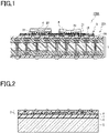
- Fig. 1 shows a semiconductor package 100 on which semiconductor elements are mounted.
- the package includes an FC-BGA circuit board component 1 as a first circuit board component and an interposer 3 as a second circuit board component.
- the FC-BGA circuit board component 1 has a surface (upper surface in Fig. 1 ) to which a surface of the interposer 3 (lower surface in Fig. 1 ) is bonded via joints 18, such as solder bumps, copper posts (copper pillars) or gold bumps.
- the interposer 3 is a thin layer having a fine wiring pattern, which is formed of only a buildup wiring layer that is a multi-wiring layer in which a plurality of insulating resin layers and wiring layers are laminated.
- an underfill 2A that is an adhesive sealing resin having insulation properties is embedded.
- semiconductor elements 4 are bonded via joints 20 formed of copper pillars, solders at the edges of the copper pillars, and the like.
- an underfill 21 is embedded in a gap between the semiconductor elements 4 and the interposer 3.
- the underfill 2A is a material used for fixing the FC-BGA circuit board component 1 and the interposer 3 and sealing the joints 18.
- the material that can be used for the underfill 2A may be obtained, for example, by adding silica, titanium oxide, aluminum oxide, magnesium oxide, zinc oxide, or the like, as a filler, to one of an epoxy resin, urethane resin, silicone resin, polyester resin, oxetane resin, and maleimide resin, or a mixture of two or more these resins.
- the underfill 2A can be formed by filling the above materials in liquid form in the gap between the FC-BGA circuit board component 1 and the interposer 3, followed by curing.
- the underfill 21 is an adhesive used for fixing the semiconductor chips 4 to the interposer 3 and sealing the joints 20, and is made of a material similar to that of the underfill 2A.
- an anisotropically conductive film (ACF) or a film-like connecting material (NCF), i.e., a sheet-like film may be arranged in a space in advance before bonding to thereby fill the space with a sheet-like film when bonding
- NCP non-conductive paste
- a liquid-form resin may be arranged in a space in advance before bonding to thereby fill the space with a liquid resin when bonding.
- the intervals of the joints 20 connecting between the interposer 3 and the semiconductor elements 4 are generally smaller than the intervals of the joints 18 connecting between the interposer 3 and the FC-BGA circuit board component 1. Therefore, the surface (upper surface in Fig. 1 ) of the interposer 3, i.e., the surface contacting the semiconductor elements 4, is required to have a finer wiring pattern than the other surface (lower surface in Fig. 1 ) thereof, i.e., the surface contacting the FC-BGA circuit board component 1.
- the interposer 3 is required to have a wiring pattern with a width of 2 ⁇ m or more and 6 ⁇ m or less.
- the insulating film between the wiring components is required to have a thickness of 2.5 ⁇ m.
- the thickness of one layer including the wiring pattern will be 4.5 ⁇ m. If a five-layer interposer 3 is formed, with one layer having this thickness, the interposer 3 will have a total thickness of about 25 ⁇ m.
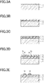
- the total thickness of the interposer 3 will be 25 ⁇ m which is so thin that it is difficult to bond the interposer 3 as it is to the FC-BGA circuit board component 1. Therefore, a support 5 may be effectively used to ensure rigidity of the interposer 3. Also, in order to form a wiring pattern having a width and a height of about 2 ⁇ m, the support 5 is required to be flat. For the reasons provided above, as shown in Fig. 2 , the interposer 3 is formed on a rigid and flat support 5 via a release layer 6, a protective layer 7, and a seed layer 8. It should be noted that other layers than the release layer 6, the protective layer 7, and the seed layer 8 may be formed on the support 5.
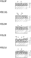
- a release layer 6 which is necessary for releasing the support 5 in a later step is formed on a surface of a support 5.
- the release layer 6 may be, for example, made of a resin that can be released after being heated or altered due to absorption of light such as UV light, or a resin that can be released after foaming due to heat. If a resin that becomes releasable due to UV light or the like is used, the support 5 can be removed from the laminate of an interposer 3 and an FC-BGA circuit board component 1 by applying light to a surface of the support 5 facing away from the surface provided with the release layer 6.
- the support 5 is required to be optically transparent and thus may be made of glass, for example.
- Glass has good flatness and is suitable for forming a fine pattern on the interposer 3.
- glass has a small coefficient of thermal expansion (CTE) and is unlikely to be strained and accordingly ensures excellent pattern arrangement accuracy and flatness.
- CTE coefficient of thermal expansion
- the thickness of the glass is preferred to be large from the perspective of minimizing the occurrence of warpage in the preparation process and thus is preferred to be, for example, 0.7 mm or more, and is particularly preferred to be 1.1 mm or more.
- the CTE of the glass is preferred to be 3 ppm or more and 15 ppm or less and is particularly preferred to be about 9 ppm from the perspective of CTE of the FC-BGA circuit board component 1 and semiconductor elements 4.
- the support 5 can be removed by heating the laminate of the interposer 3 and the FC-BGA circuit board component 1.
- the support 5 may be made of, for example, metal, ceramics, or the like which are less likely to be strained.
- a resin that becomes releasable due to absorption of UV light is used as the release layer 6, and glass is used as the support 5.
- the protective layer 7 serves as a layer for protecting the interposer 3 when releasing the support 5 in a later step.
- the protective layer 7 may be made of a resin that is one of an epoxy resin, acrylic resin, urethane resin, silicone resin, polyester resin, and oxetane resin, or a mixture of two or more of these resins.
- the protective layer 7 can be formed as appropriate according to the shape of the resin, using spin coating, a lamination process, or the like. In the present embodiment, the protective layer 7 is formed through a lamination process using an acrylic resin.
- a seed layer 8 is formed on the protective layer 7 in a vacuum.
- the seed layer 8 serves as a power supply layer for electroplating in a step of forming a wiring pattern.
- the seed layer 8 may be made of, for example, Cu, Ni, Al, Ti, Cr, Mo, W, Ta, Au, Ir, Ru, Pd, Pt, AlSi, AlSiCu, AlCu, NiFe, ITO, IZO, AZO, ZnO, PZT, TiN, Cu 3 N 4 , or a Cu alloy which are used singly or in combination of two or more, and can be formed by, for example, sputtering, CVD, or the like.
- a titanium layer and then a copper layer are sequentially formed by sputtering, from the perspective of electrical characteristics, ease of preparation, cost, and the like.
- the total thickness of the titanium layer and the copper layer is preferred to be 1 ⁇ m or less as a power supply layer for electroplating.
- the thickness of Ti is 50 nm and that of Cu is 300 nm.
- a resist pattern 9 is formed and conductive elements 10 serving as first electrodes are formed in respective openings 9a of the resist pattern 9.
- the conductive elements 10 are used as electrodes to achieve bonding with the semiconductor elements 4.
- the electroplating may be electroplating of nickel, copper, chromium, Pd, gold, rhodium, iridium, or the like.
- electroplating of copper is preferred because it is easy and inexpensive and achieves good electrical conductivity.
- the thickness of the electroplated copper is preferred to be 1 ⁇ m or more and 30 ⁇ m or less from the perspective of connection reliability for circuits, manufacturing cost, and the like.
- an insulating resin layer 11 is formed.
- the insulating resin layer 11 is formed so that the conductive elements 10 are embedded therein.
- the insulating resin layer 11 of the present embodiment is formed by spin-coating a photosensitive epoxy resin, for example. Photosensitive epoxy resins are cured at relatively low temperatures, and less likely to shrink due to curing after formation, and thus are excellent in fine pattern formation thereafter.
- the insulating resin layer 11 may also be formed by compressing and curing an insulating resin film using a vacuum laminator. In this case, an insulating film having good flatness can be formed. Also, for example, a polyimide may be used as an insulating resin.
- openings 11a are formed in the insulating resin layer 11 using photolithography or the like so as to be located above the respective conductive elements 10.
- the openings 11a may be subjected to plasma treatment for the purpose of removing residues produced during development.
- a seed layer 12 is provided on the surface of the insulating resin layer 11 and on the conductive elements 10 in the openings 11a.
- the seed layer 12 has a composition and a thickness which are similar to those of the seed layer 8 described above, but they may be appropriately changed as necessary.
- the seed layer 12 is formed by sputtering so that the thickness of Ti will be 50 nm and that of Cu will be 300 nm.
- a resist pattern 13 is formed on the seed layer 12 and conductive elements 14 serving as a wiring layer are formed by electroplating in openings 13a of the resist pattern 13.
- the conductive elements 14 serve as a wiring layer in the interposer 3.
- copper is used for the conductive elements 14.
- the resist pattern 13 is removed. Then, unnecessary portions of the seed layer 12 are etched away.
- insulating resin layers 11 and conductive elements 14 are laminated.
- conductive elements 15 located on the outermost surface are used as electrodes to be bonded to the FC-BGA circuit board component 1.
- an outermost insulating resin layer 16 is provided on the surface of the insulating resin layer 11 and on the conductive elements 15.
- the outermost insulating resin layer 16 is provided with openings 16a formed by exposure, development, and the like, so that the conducive elements 15 are partially exposed and the insulating resin layers 11 are covered.
- the outermost insulating resin layer 16 is formed using a photosensitive epoxy resin. The same material as that of the insulating resin layer 11 may be used for the outermost insulating resin layer 16.
- surface treatment films 17 are provided on the conductive elements 15 in the respective openings 16a to improve oxidation resistance of the surfaces of the conductive elements 15 and wettability of solder bumps.
- the surface treatment films 17 are formed by electroless plating of Ni/Pd/Au.
- OSP surface treatment using organic solderability preservative/water-soluble preflux
- Electroless plating of tin, electroless plating of Ni/Au, or electroless plating of other materials may be selected as appropriate according to usage.
- a solder material is mounted on the surface treatment films 17, melted, cooled, and fixed to form joints 18a that are solder bumps for bonding between the FC-BGA circuit board component 1 and the interposer 3.
- second electrodes are each configured by a conductive element 15, a surface treatment film 17, and a joint 18a.
- an interposer 3 formed on the support 5 can be obtained.
- the FC-BGA circuit board component 1 prepared herein includes joints 18b, as third electrodes, which are designed to match the respective joints 18a of the interposer 3.
- the interposer 3 formed on the support 5 is disposed on and bonded to such an FC-BGA circuit board component 1 to form joints 18.
- the interposer 3 is mounted on the FC-BGA circuit board component 1 using a mounter, and the joints 18a of the interposer 3 and the joints 18b of the FC-BGA circuit board component 1 are melted and bonded together using a conveyor type heating device (reflow) to form the joints 18.
- a flux cleaning step is performed after the bonding step.
- a direct pass cleaning device is preferred to be used; however, an ultrasonic cleaning device may be used.
- laser light L that is UV light is applied to the release layer 6 via the support 5 to release the support 5.
- the laser light F is applied to a surface of the interposer 3 (upper surface in Fig. 5A ), i.e., the surface facing away from the surface to be connected to the FC-BGA circuit board component 1, via the support 5 to bring the release layer 6 formed at the interface with the support 5 into a releasable state.
- the support 5 is detached via the release layer 6 (this step will be termed support release step hereinafter).
- detachment of the support 5 depends on the characteristics of the release layer 6. If the retainability of the release layer 6 is deteriorated, the support 5 can be easily released when pulled. If the release layer 6 has high retainability, a sheet having high adhesion, for example, is adhered to the support 5 and pulled to release the support 5.
- the underfill 2A is filled in the gap between the interposer 3 and the FC-BGA circuit board component 1 (this step will be termed resin supply step hereinafter).
- the underfill 2A is supplied using a dispenser that presses and injects the material with a syringe, and filled in the gap.
- the underfill 2A can be applied so as to be located adjacent to the interposer 3 using an air dispenser type or jet dispenser type underfill coating device, or the like.
- the applied underfill 2A is filled in the gap between the interposer 3 and the FC-BGA circuit board component 1 due to the capillary phenomenon.
- the underfill 2A to be filled in the gap between the interposer 3 and the FC-BGA circuit board component 1 is supplied a plurality of times with a three or more-second interval therebetween, so that the underfill 2A will be prevented from rising up over the interposer 3.
- the supplied underfill 2A is heated at a temperature that is not less than the curing temperature of the underfill 2A and then cured to fix the interposer 3 and the FC-BGA circuit board component 1 and seal the joints 18 (this step will be termed resin curing step hereinafter).
- the protective layer 7 is removed, followed by removing the seed layer 8, as shown in Fig. 5D , to obtain a circuit board 22A.
- the protective layer 7 made of an acrylic resin is removed using an alkaline solvent (1% NaOH and 2.3% TMAH). Titanium and copper which sequentially form the seed layer 8 from the protective layer 7 side are respectively dissolved and removed using an alkaline etching agent and an acid etching agent.
- the conductive elements 10 exposed to the surface may be further surfacetreated such as by electroless plating of Ni/Pd/Au, OSP, electroless plating of tin, electroless plating of Ni/Au, or the like to prevent oxidation and improve wettability of the solder bumps.
- the support release step is sequentially followed by the resin supply step and the resin curing step. This method can prevent the underfill 2A from enclosing the support 5 and from fixing and holding the support 5 due to curing of the underfill 2A.
- yield can be improved in the step of releasing the support 5 to produce circuit boards with high productivity.
- the joints 18 can be protected from the alkaline etching agent and the acid etching agent used for removing the protective layer 7 and the seed layer 8, thereby preventing connection reliability from being deteriorated.
- Fig. 6 shows a circuit board 22B of a semiconductor package 100B according to the present embodiment.
- an underfill 2B is formed so as to be located closer to the semiconductor elements 4 (upper side in Fig. 6 ) than to the surface of the interposer 3 connected to the semiconductor elements 4 (upper surface in Fig. 6 ).
- the circuit board 22B has a structure similar to the circuit board 22A of the semiconductor package 100A of the embodiment described above.
- steps up to the bonding step of forming the joints 18 by bonding the joints 18a of the interposer 3 with the joints 18b of the FC-BGA circuit board component 1 are the same as those of the production method for the circuit board 22A of the embodiment described above.
- the underfill 2B is supplied to enclose the interposer 3, the seed layer 8, the protective layer 7, the release layer 6, and the support 5, while sealing the gap between the interposer 3 and the FC-BGA circuit board component 1 to temporarily fix the interposer 3 formed on the support 5 and the FC-BGA circuit board component 1 (this step will be termed resin supply step hereinafter).
- the underfill 2B is heated to the curing temperature or more, and then cured to fix the interposer 3 and the FC-BGA circuit board component 1 and seal the joints 18 (this step will be termed resin curing step hereinafter).
- the protective layer 7 and the seed layer 8 are removed as in the above embodiment.
- the circuit board 22B in which the interposer 3 and the FC-BGA circuit board component 1 are bonded together.
- the resin supply step is followed by the resin adhesion lowering step which is sequentially followed by the support release step and the resin curing step.
- This method can release the support 5 from the underfill 2B adhered to the periphery of the support 5 and facilitate detachment of the support 5.
- yield can also be improved in the step of releasing the support 5 to produce circuit boards with high productivity.
- Fig. 8 shows a circuit board 22C of a semiconductor package 100C according to the present embodiment.
- an underfill 2C is formed so as to be located closer to the FC-BGA circuit board component 1 (lower side in Fig. 8 ) than to the surface of the interposer 3 connected to the semiconductor elements 4 (upper surface in Fig. 8 ).
- the circuit board 22C has a structure similar to the circuit boards 22A and 22B of the semiconductor packages 100A and 100B of the embodiments described above.
- steps up to the bonding step of forming the joints 18 by bonding the joints 18a of the interposer 3 with the joints 18b of the FC-BGA circuit board component 1 are the same as those of the production methods for the circuit boards 22A and 22B of the embodiments described above.
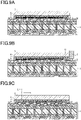
- the underfill 2C is filled in the gap between the interposer 3 and the FC-BGA circuit board component 1 (this step will be termed resin supply step hereinafter).
- an underfill removal jig T such as a squeegee, is placed so as to contact the side surfaces (right and left surfaces and front and back surfaces as viewed in Fig. 9B ) of the interposer 3.
- the jig is slidably moved over the outer periphery of the interposer 3 to scrape and remove the underfill 2C adhered to the side surfaces of the interposer 3, or at least the underfill 2C adhered closer to the support 5 than to the insulating resin layers 11 (this step will be termed resin removal step hereinafter).
- the seed layer 8, the protective layer 7, and the release layer 6 are located closer to the support 5 than to the insulating resin layers 11, at least the underfill 2C adhered to the outer peripheries of the seed layer 8, the protective layer 7, and the release layer 6 is removed.
- only the underfill 2C located closer to the support 5 than to the insulating resin layers 11 is removed without removing the underfill 2C located on the side surfaces of the insulating resin layers 11.
- the underfill removal jig T for example, a flat squeegee may be used. Such a squeegee is preferred to be tapered in the thickness direction at an end portion of the squeegee. A squeegee can be appropriately selected according to various conditions.
- the underfill removal jig T is preferred to be made of a material having relatively low hardness.
- the material may be silicone rubber, urethane, Teflon (trademark), or other rubbers and plastics.
- the underfill 2C is cured by heating to fix the interposer 3 and the FC-BGA circuit board component 1 and seal the joints 18 (this step will be termed resin curing step hereinafter).
- laser light L is applied to the release layer 6 via the support 5.
- the support 5 is released as in the above embodiments.
- the protective layer 7 and the seed layer 8 are removed as in the above embodiments (this step will be termed support release step hereinafter).
- the resin supply step is followed by the resin removal step of removing at least the underfill 2C located closer to the support 5 on the side surfaces of the interposer 3 than to the insulating resin layers 11, which is sequentially followed by the resin curing step and the support release step. Therefore, the shape of the underfill 2C after being cured can be controlled, regardless of the shape of the underfill 2C when supplied. Accordingly, the underfill 2C is prevented from fixing and holding the support 5 during curing.
- irradiation of the release layer 6 with the laser light L can easily and reliably release the support 5 from the protective layer 7 as in the above embodiments.
- yield can be improved in the step of releasing the support 5 to produce circuit boards with high productivity as in the above embodiments.
- the underfill removal jig T is enhanced in followability to the shapes of the side surfaces of the interposer 3. Therefore, the underfill 2C can be more reliably removed.
- a material having relatively high hardness may be used for the underfill removal jig T.
- any of Cu, Ti, Sn, Fe, Al, Cr, Ag, Au, Pt, Ni and Mn, or an alloy of two or more materials, or a complex of two or more materials, or other materials may be used. If a material having a relatively high hardness is used for the underfill removal jig T, deformation of the underfill removal jig T when removing the underfill 2C can be minimized, and position accuracy of the jig T when removing the underfill 2C can be enhanced.
- a syringe needle connected to a suction mechanism may be used as the underfill removal jig T, so that the underfill 2C adhered to the outer periphery of the interposer 3 can be sucked and removed.
- Use of such a syringe needle connected to a suction mechanism as the underfill removal jig T can eliminate the issues of the underfill 2C spreading over the underfill removal jig T and re-adhering to the interposer 3 while being removed, and the removed underfill 2 spreading over the FC-BGA circuit board component 1 in the width direction.
- a step of forming a mask may be performed prior to the resin supply step, and then the resin removal step may be performed, sequentially followed by a step of removing the mask, and the resin curing step.
- a releasable first mask 23 may be partially formed on the surface of the FC-BGA circuit board component 1 facing the interposer 3, and a releasable second mask 24 may be formed on the surface of the support 5 facing away from the surface provided with the interposer 3.
- the first and second masks 23 and 24 may be formed using a material that can be patterned and can be released.
- a photosensitive dry film resist for forming wiring patterns, a liquid photosensitive resist, or the like may be used. If a photosensitive dry film resist is used, the first and second masks 23 and 24 may be formed through roll lamination, vacuum lamination, or the like. If a liquid photosensitive resist is used, the masks may be formed through spin coating, slit coating, screen printing, gravure offset printing, or the like.
- an opening 23a is formed by photolithography, for filling the underfill 2C therefrom.
- the opening 23a of the first mask 23 may be formed throughout the outer periphery of the interposer 3, or may be formed only in a portion of the outer periphery.
- the first mask 23 has a thickness that is not more than the thickness of the interposer 3.
- the underfill 2C is filled in the gap between the interposer 3 and the FC-BGA circuit board component 1 from such an opening 23a of the first mask 23, and the underfill 2C adhered to the outer periphery of the interposer 3 is removed using the underfill removal jig T in the manner described above.
- the underfill removal jig T is preferred to have a size (height) enabling the jig to abut against the first mask 23.
- the first and second masks 23 and 24 are removed.
- the first and second masks 23 and 24 are removed using a stripping solution which is used for stripping photosensitive resins.
- the first mask 23 is partially formed on the surface of the FC-BGA circuit board component 1 facing the interposer 3 prior to the resin supply step, and then the resin removal step is performed, followed by removing the first mask 23 prior to the resin curing step. Therefore, the shape of the underfill 2C after being cured can be controlled with high accuracy.
- the first mask 23 may be formed to have substantially the same thickness as that of the outermost insulating resin layer 16 of the interposer 3, so that the underfill removal jig T can be disposed abutting against the first mask 23. This enables removal of the underfill 2C located up to the boundary between the insulating resin layers 11 and the outermost insulating resin layer 16, i.e., up to the lowest level of the insulating resin layers 11.
- the second mask 24 is formed on the surface of the support 5 facing away from the surface provided with the interposer 3 prior to the resin supply step, and then the resin removal step is performed, followed by removing the second mask 24 prior to the resin curing step. Therefore, the underfill 2C that has risen up over the surface of the support 5 facing away from the surface provided with the interposer 3 can be easily removed.
- the present invention can be applied to semiconductor devices including a circuit board which is provided with an interposer, or the like intervened between a main circuit board component and IC chips.
Landscapes
- Engineering & Computer Science (AREA)
- Microelectronics & Electronic Packaging (AREA)
- Manufacturing & Machinery (AREA)
- Encapsulation Of And Coatings For Semiconductor Or Solid State Devices (AREA)
- Production Of Multi-Layered Print Wiring Board (AREA)
- Combinations Of Printed Boards (AREA)
Abstract
Description
- The present invention relates to methods of producing circuit boards.
- In recent years, with the progress of high speed and high integration of semiconductor devices, FC-BGA (flip chip-ball grid array) circuit board components are required to have narrow-pitch connection terminals for semiconductor elements and to have fine circuit board wiring patterns. On the other hand, for connection with mother boards, FC-BGA circuit board components are required to have connection terminals with pitches remaining substantially unchanged from conventional art.
- In order to achieve narrow-pitch connection terminals for semiconductor elements and to achieve fine circuit board wiring patterns,
PTL 1, for example, proposes a method in which a wiring pattern is formed on a silicon material to obtain a substrate (silicon interposer) for connection with semiconductor elements, and this substrate is connected to an FC-BGA circuit board component. Furthermore, PTL 2, for example, proposes a method in which a surface of an FC-BGA circuit board component is flattened such as by chemical mechanical polishing (CMP) and then a fine wiring pattern is formed. Also,PTL 3, for example, proposes a method in which a substrate including a fine wiring pattern layer (interposer) is formed on a support and then mounted on an FC-BGA circuit board component, followed by releasing the support to form a narrow-pitch circuit board. -
- PTL 1:
JP 2002-280490 A - PTL 2:
JP 2014-225671 A - PTL 3:
WO2018/047861 - In the method disclosed in
PTL 1, the silicon interposer is prepared using a silicon wafer and using equipment for preprocessing semiconductors. Silicon wafers are limited in shape and size and the number of interposers that can be prepared from one wafer is small. In addition, since the preparation equipment is expensive, prepared interposers are also expensive. Problematically, silicon wafers, which are made of semiconductor materials, tend to deteriorate in transmission characteristics. - The method disclosed in PTL 2 raises no issue of transmission characteristics deterioration as in the method disclosed in
PTL 1. However, this method raises an issue of lowering yield due to production defects in the FC-BGA circuit board components, coupled with defects caused when forming the difficult fine wiring patterns, or an issue of mounting semiconductor elements on an FC-BGA circuit board component that may have warpage or strain. - The method disclosed in
PTL 3 raises no issue of transmission characteristics deterioration as in the method disclosed inPTL 1, or issue of lowering yield as in the method disclosed in PTL 2. However, the method disclosed inPTL 3 raises an issue of easily causing defects in the step of releasing a support and thus lowering yield. - The present invention has been made in light of the issues set forth above and aims to provide a method of producing circuit boards with high productivity by improving yield in the step of releasing a support.
- In order to solve the issues set forth above, the present invention provides a method of producing circuit boards, the circuit boards each including a first circuit board component and a second circuit board component, the second circuit board component having a bonding surface on which a wiring pattern finer than that of the first circuit board component is formed and to which the first circuit board component is bonded, the second circuit board component having a surface on which semiconductor elements are mounted that faces away from the bonding surface. The method is characterized by a second circuit board component preparation step of preparing the second circuit board component by performing a step of forming first electrodes on a support via a release layer for bonding to the semiconductor elements, a step of forming a multi-wiring layer, which is a laminate of a plurality of insulating resin layers and wiring layers, on the first electrodes, and a step of forming second electrodes on the multi-wiring layer for bonding to the first circuit board component; and a bonding step of bonding third electrodes of the first circuit board component to be connected to the second circuit board component, with the respective second electrodes of the second circuit board component. These steps are followed by a resin supply step of filling a sealing resin in a gap between the first circuit board component and the second circuit board component; a resin curing step of curing the sealing resin; and a support release step of releasing the support from the second circuit board component via the release layer, which are performed through any one of the following sequences which are: (1) the support release step, the resin supply step, and the resin curing step; (2) the resin supply step, the support release step, and the resin curing step; and (3) the resin supply step, a resin removal step of removing the sealing resin adhered to outer peripheries of the second circuit board component, the release layer, and the support, the resin curing step, and the support release step.
- According to the method of producing circuit boards of the present invention, yield can be improved in the step of releasing a support to thereby produce circuit boards with high productivity.
-
-
Fig. 1 is a schematic cross-sectional view illustrating a structural example of a semiconductor package produced using a first embodiment of the method of producing circuit boards of the present invention. -
Fig. 2 is a schematic cross-sectional view illustrating a structural example of an interposer used in the first embodiment of the method of producing circuit boards of the present invention. -
Fig. 3A is a cross sectional view illustrating a preparation procedure of the interposer illustrated inFig. 2 . -
Fig. 3B is a cross-sectional view illustrating the preparation procedure followingFig. 3A . -
Fig. 3C is a cross-sectional view illustrating the preparation procedure followingFig. 3B . -
Fig. 3D is a cross-sectional view illustrating the preparation procedure followingFig. 3C . -
Fig. 3E is a cross-sectional view illustrating the preparation procedure followingFig. 3D . -
Fig. 3F is a cross-sectional view illustrating the preparation procedure followingFig. 3E . -
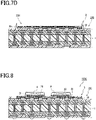
Fig. 3G is a cross-sectional view illustrating the preparation procedure followingFig. 3F . -
Fig. 3H is a cross-sectional view illustrating the preparation procedure followingFig. 3G . -
Fig. 3I is a cross-sectional view illustrating the preparation procedure followingFig. 3H . -
Fig. 3J is a cross-sectional view illustrating the preparation procedure followingFig. 3J . -
Fig. 3K is a cross-sectional view illustrating the preparation procedure followingFig. 3J . -
Fig. 3L is a cross-sectional view illustrating the preparation procedure followingFig. 3K . -
Fig. 3M is a cross-sectional view illustrating the preparation procedure followingFig. 3L . -
Fig. 3N is a cross-sectional view illustrating the preparation procedure followingFig. 3M . -
Fig. 4A is a cross-sectional view illustrating the preparation procedure followingFig. 3N . -
Fig. 4B is a cross-sectional view illustrating the preparation procedure followingFig. 4A . -
Fig. 5A is a cross-sectional view illustrating the preparation procedure followingFig. 4B . -
Fig. 5B is a cross-sectional view illustrating the preparation procedure followingFig. 5A . -
Fig. 5C is a cross-sectional view illustrating the preparation procedure followingFig. 5B . -
Fig. 5D is a cross-sectional view illustrating the preparation procedure followingFig. 5C . -
Fig. 6 is a schematic cross-sectional view illustrating a structural example of a semiconductor package produced using a second embodiment of the method of producing circuit boards of the present invention. -
Fig. 7A is a cross-sectional view illustrating a preparation procedure followingFig.4B , according to the second embodiment of the method of producing circuit boards of the present invention. -
Fig. 7B is a cross-sectional view illustrating the preparation procedure followingFig. 7A . -
Fig. 7C is a cross-sectional view illustrating the preparation procedure followingFig. 7B . -
Fig. 7D is a cross-sectional view illustrating the preparation procedure followingFig. 7C . -
Fig. 8 is a schematic cross-sectional view illustrating a structural example of a semiconductor package produced using a third embodiment of the method of producing circuit boards of the present invention. -
Fig. 9A is a cross-sectional view illustrating a preparation procedure followingFig.4B , according to the third embodiment of the method of producing circuit boards of the present invention. -
Fig. 9B is a cross-sectional view illustrating the preparation procedure followingFig. 9A . -
Fig. 9C is a cross-sectional view illustrating the preparation procedure followingFig. 9B . -
Fig. 9D is a cross-sectional view illustrating the preparation procedure followingFig. 9C . -
Fig. 9E is a cross-sectional view illustrating the preparation procedure followingFig. 9D . -
Fig. 10 is a cross-sectional view illustrating a preparation procedure according to Example 3 of the third embodiment of the method of producing circuit boards of the present invention. - With reference to the drawings, some embodiments of a method of producing circuit boards of the present invention will be described. However, the present invention should not be construed as limited to only the following embodiments described based on the drawings. For the sake of clarity, the drawings are illustrated in an exaggerated manner as appropriate.
- Referring to
Figs. 1, 2 ,3A to 3N ,4A, 4B , and5A to 5D , a first embodiment of a method of producing circuit boards of the present invention will be described. - A circuit board produced using a production method according to the present embodiment has a structure in which a first circuit board component is bonded to a bonding surface of a second circuit board component on which a wiring pattern finer than that of the first circuit board component is formed, and semiconductor elements are mounted to a surface of the second circuit board component facing away from the bonding surface.
- Specifically,
Fig. 1 shows a semiconductor package 100 on which semiconductor elements are mounted. The package includes an FC-BGAcircuit board component 1 as a first circuit board component and aninterposer 3 as a second circuit board component. The FC-BGAcircuit board component 1 has a surface (upper surface inFig. 1 ) to which a surface of the interposer 3 (lower surface inFig. 1 ) is bonded viajoints 18, such as solder bumps, copper posts (copper pillars) or gold bumps. Theinterposer 3 is a thin layer having a fine wiring pattern, which is formed of only a buildup wiring layer that is a multi-wiring layer in which a plurality of insulating resin layers and wiring layers are laminated. - In a gap between the FC-BGA
circuit board component 1 and theinterposer 3, anunderfill 2A that is an adhesive sealing resin having insulation properties is embedded. On the other surface of the interposer 3 (the upper surface inFig. 1 ), i.e., on the surface facing away from the bonding surface to which the FC-BGAcircuit board component 1 is connected,semiconductor elements 4 are bonded viajoints 20 formed of copper pillars, solders at the edges of the copper pillars, and the like. In a gap between thesemiconductor elements 4 and theinterposer 3, anunderfill 21 is embedded. - The
underfill 2A is a material used for fixing the FC-BGAcircuit board component 1 and theinterposer 3 and sealing thejoints 18. The material that can be used for theunderfill 2A may be obtained, for example, by adding silica, titanium oxide, aluminum oxide, magnesium oxide, zinc oxide, or the like, as a filler, to one of an epoxy resin, urethane resin, silicone resin, polyester resin, oxetane resin, and maleimide resin, or a mixture of two or more these resins. Theunderfill 2A can be formed by filling the above materials in liquid form in the gap between the FC-BGAcircuit board component 1 and theinterposer 3, followed by curing. - The
underfill 21 is an adhesive used for fixing thesemiconductor chips 4 to theinterposer 3 and sealing thejoints 20, and is made of a material similar to that of theunderfill 2A. Instead of filling the gaps with theunderfills - The intervals of the
joints 20 connecting between theinterposer 3 and thesemiconductor elements 4 are generally smaller than the intervals of thejoints 18 connecting between theinterposer 3 and the FC-BGAcircuit board component 1. Therefore, the surface (upper surface inFig. 1 ) of theinterposer 3, i.e., the surface contacting thesemiconductor elements 4, is required to have a finer wiring pattern than the other surface (lower surface inFig. 1 ) thereof, i.e., the surface contacting the FC-BGAcircuit board component 1. - For example, in order to meet the usage of currently used high bandwidth memories (HBMs), the
interposer 3 is required to have a wiring pattern with a width of 2 µm or more and 6 µm or less. In order to match the characteristic impedance to 50Ω when the wiring pattern width is 2 µm and the wiring pattern height is 2 µm, the insulating film between the wiring components is required to have a thickness of 2.5 µm. Thus, the thickness of one layer including the wiring pattern will be 4.5 µm. If a five-layer interposer 3 is formed, with one layer having this thickness, theinterposer 3 will have a total thickness of about 25 µm. - As mentioned above, the total thickness of the
interposer 3 will be 25 µm which is so thin that it is difficult to bond theinterposer 3 as it is to the FC-BGAcircuit board component 1. Therefore, asupport 5 may be effectively used to ensure rigidity of theinterposer 3. Also, in order to form a wiring pattern having a width and a height of about 2 µm, thesupport 5 is required to be flat. For the reasons provided above, as shown inFig. 2 , theinterposer 3 is formed on a rigid andflat support 5 via arelease layer 6, aprotective layer 7, and aseed layer 8. It should be noted that other layers than therelease layer 6, theprotective layer 7, and theseed layer 8 may be formed on thesupport 5. - Referring to
Figs. 3A to 3N , a method of preparing the interposer 3 (preparation steps for the second circuit board component) according to the present embodiment will be described. - First, as shown in
Fig. 3A , arelease layer 6 which is necessary for releasing thesupport 5 in a later step is formed on a surface of asupport 5. - The
release layer 6 may be, for example, made of a resin that can be released after being heated or altered due to absorption of light such as UV light, or a resin that can be released after foaming due to heat. If a resin that becomes releasable due to UV light or the like is used, thesupport 5 can be removed from the laminate of aninterposer 3 and an FC-BGAcircuit board component 1 by applying light to a surface of thesupport 5 facing away from the surface provided with therelease layer 6. - In this case, the
support 5 is required to be optically transparent and thus may be made of glass, for example. Glass has good flatness and is suitable for forming a fine pattern on theinterposer 3. Also, glass has a small coefficient of thermal expansion (CTE) and is unlikely to be strained and accordingly ensures excellent pattern arrangement accuracy and flatness. - If glass is used as the
support 5, the thickness of the glass is preferred to be large from the perspective of minimizing the occurrence of warpage in the preparation process and thus is preferred to be, for example, 0.7 mm or more, and is particularly preferred to be 1.1 mm or more. Furthermore, the CTE of the glass is preferred to be 3 ppm or more and 15 ppm or less and is particularly preferred to be about 9 ppm from the perspective of CTE of the FC-BGAcircuit board component 1 andsemiconductor elements 4. - If a resin that foams due to heat is used for the
release layer 6, thesupport 5 can be removed by heating the laminate of theinterposer 3 and the FC-BGAcircuit board component 1. In this case, thesupport 5 may be made of, for example, metal, ceramics, or the like which are less likely to be strained. - In the present embodiment, a resin that becomes releasable due to absorption of UV light is used as the
release layer 6, and glass is used as thesupport 5. - Next, as shown in
Fig. 3B , aprotective layer 7 is formed on therelease layer 6. Theprotective layer 7 serves as a layer for protecting theinterposer 3 when releasing thesupport 5 in a later step. For example, it may be made of a resin that is one of an epoxy resin, acrylic resin, urethane resin, silicone resin, polyester resin, and oxetane resin, or a mixture of two or more of these resins. - These resins can be removed after releasing the
interposer 3 from thesupport 5. Theprotective layer 7 can be formed as appropriate according to the shape of the resin, using spin coating, a lamination process, or the like. In the present embodiment, theprotective layer 7 is formed through a lamination process using an acrylic resin. - Next, as shown in
Fig. 3C , aseed layer 8 is formed on theprotective layer 7 in a vacuum. Theseed layer 8 serves as a power supply layer for electroplating in a step of forming a wiring pattern. Theseed layer 8 may be made of, for example, Cu, Ni, Al, Ti, Cr, Mo, W, Ta, Au, Ir, Ru, Pd, Pt, AlSi, AlSiCu, AlCu, NiFe, ITO, IZO, AZO, ZnO, PZT, TiN, Cu3N4, or a Cu alloy which are used singly or in combination of two or more, and can be formed by, for example, sputtering, CVD, or the like. - In the present embodiment, a titanium layer and then a copper layer are sequentially formed by sputtering, from the perspective of electrical characteristics, ease of preparation, cost, and the like. The total thickness of the titanium layer and the copper layer is preferred to be 1 µm or less as a power supply layer for electroplating. In the present embodiment the thickness of Ti is 50 nm and that of Cu is 300 nm.
- Next, as shown in
Fig. 3D , a resistpattern 9 is formed andconductive elements 10 serving as first electrodes are formed inrespective openings 9a of the resistpattern 9. Theconductive elements 10 are used as electrodes to achieve bonding with thesemiconductor elements 4. The electroplating may be electroplating of nickel, copper, chromium, Pd, gold, rhodium, iridium, or the like. In particular, electroplating of copper is preferred because it is easy and inexpensive and achieves good electrical conductivity. The thickness of the electroplated copper is preferred to be 1 µm or more and 30 µm or less from the perspective of connection reliability for circuits, manufacturing cost, and the like. After that, as shown inFig. 3E , the resistpattern 9 is removed. - Next, as shown in
Fig. 3F , an insulatingresin layer 11 is formed. The insulatingresin layer 11 is formed so that theconductive elements 10 are embedded therein. The insulatingresin layer 11 of the present embodiment is formed by spin-coating a photosensitive epoxy resin, for example. Photosensitive epoxy resins are cured at relatively low temperatures, and less likely to shrink due to curing after formation, and thus are excellent in fine pattern formation thereafter. - Other than the above method, the insulating
resin layer 11 may also be formed by compressing and curing an insulating resin film using a vacuum laminator. In this case, an insulating film having good flatness can be formed. Also, for example, a polyimide may be used as an insulating resin. - Next, as shown in
Fig. 3G ,openings 11a are formed in the insulatingresin layer 11 using photolithography or the like so as to be located above the respectiveconductive elements 10. Theopenings 11a may be subjected to plasma treatment for the purpose of removing residues produced during development. - Next, as shown in
Fig. 3H , aseed layer 12 is provided on the surface of the insulatingresin layer 11 and on theconductive elements 10 in theopenings 11a. Theseed layer 12 has a composition and a thickness which are similar to those of theseed layer 8 described above, but they may be appropriately changed as necessary. In the present embodiment, theseed layer 12 is formed by sputtering so that the thickness of Ti will be 50 nm and that of Cu will be 300 nm. - Next, as shown in
Fig. 3I , a resistpattern 13 is formed on theseed layer 12 andconductive elements 14 serving as a wiring layer are formed by electroplating inopenings 13a of the resistpattern 13. Theconductive elements 14 serve as a wiring layer in theinterposer 3. In the present embodiment, copper is used for theconductive elements 14. After that, as shown inFig. 3J , the resistpattern 13 is removed. Then, unnecessary portions of theseed layer 12 are etched away. - Subsequently, the steps shown in
Figs. 3F to 3J are repeated a plurality of times to form a multi-wiring layer, as shown inFig. 3K , in which insulating resin layers 11 andconductive elements 14 are laminated. It should be noted thatconductive elements 15 located on the outermost surface are used as electrodes to be bonded to the FC-BGAcircuit board component 1. - Next, as shown in
Fig. 3L , an outermost insulatingresin layer 16 is provided on the surface of the insulatingresin layer 11 and on theconductive elements 15. The outermost insulatingresin layer 16 is provided withopenings 16a formed by exposure, development, and the like, so that theconducive elements 15 are partially exposed and the insulating resin layers 11 are covered. In the present embodiment, the outermost insulatingresin layer 16 is formed using a photosensitive epoxy resin. The same material as that of the insulatingresin layer 11 may be used for the outermost insulatingresin layer 16. - Next, as shown in
Fig. 3M ,surface treatment films 17 are provided on theconductive elements 15 in therespective openings 16a to improve oxidation resistance of the surfaces of theconductive elements 15 and wettability of solder bumps. In the present embodiment, thesurface treatment films 17 are formed by electroless plating of Ni/Pd/Au. It should be noted that OSP (surface treatment using organic solderability preservative/water-soluble preflux) films may be formed as thesurface treatment films 17. Electroless plating of tin, electroless plating of Ni/Au, or electroless plating of other materials may be selected as appropriate according to usage. - Next, as shown in
Fig. 3N , a solder material is mounted on thesurface treatment films 17, melted, cooled, and fixed to formjoints 18a that are solder bumps for bonding between the FC-BGAcircuit board component 1 and theinterposer 3. In the present embodiment, second electrodes are each configured by aconductive element 15, asurface treatment film 17, and a joint 18a. Thus, aninterposer 3 formed on thesupport 5 can be obtained. - Referring now to
Figs. 4A and 4B , steps of bonding theinterposer 3 with the FC-BGAcircuit board component 1 will be described. - The FC-BGA
circuit board component 1 prepared herein includesjoints 18b, as third electrodes, which are designed to match therespective joints 18a of theinterposer 3. As shown inFigs. 4A and 4B , theinterposer 3 formed on thesupport 5 is disposed on and bonded to such an FC-BGAcircuit board component 1 to form joints 18. Specifically, theinterposer 3 is mounted on the FC-BGAcircuit board component 1 using a mounter, and thejoints 18a of theinterposer 3 and thejoints 18b of the FC-BGAcircuit board component 1 are melted and bonded together using a conveyor type heating device (reflow) to form thejoints 18. - If a flux is used for solder bonding, it is preferred that a flux cleaning step is performed after the bonding step. For the flux cleaning step, a direct pass cleaning device is preferred to be used; however, an ultrasonic cleaning device may be used.
- Referring to
Figs. 5A to 5D , a method of placing theunderfill 2A and a method of removing thesupport 5 according to the present embodiment will be described. - First, as shown in
Fig. 5A , laser light L that is UV light is applied to therelease layer 6 via thesupport 5 to release thesupport 5. Specifically, the laser light F is applied to a surface of the interposer 3 (upper surface inFig. 5A ), i.e., the surface facing away from the surface to be connected to the FC-BGAcircuit board component 1, via thesupport 5 to bring therelease layer 6 formed at the interface with thesupport 5 into a releasable state. Then, as shown inFig. 5B , thesupport 5 is detached via the release layer 6 (this step will be termed support release step hereinafter). - It should be noted that detachment of the
support 5 depends on the characteristics of therelease layer 6. If the retainability of therelease layer 6 is deteriorated, thesupport 5 can be easily released when pulled. If therelease layer 6 has high retainability, a sheet having high adhesion, for example, is adhered to thesupport 5 and pulled to release thesupport 5. - Next, as shown in
Fig. 5C , theunderfill 2A is filled in the gap between theinterposer 3 and the FC-BGA circuit board component 1 (this step will be termed resin supply step hereinafter). Theunderfill 2A is supplied using a dispenser that presses and injects the material with a syringe, and filled in the gap. Theunderfill 2A can be applied so as to be located adjacent to theinterposer 3 using an air dispenser type or jet dispenser type underfill coating device, or the like. The appliedunderfill 2A is filled in the gap between theinterposer 3 and the FC-BGAcircuit board component 1 due to the capillary phenomenon. - If the supply amount of the
underfill 2A per unit time is excessively large, theunderfill 2A may rise up over theinterposer 3. Therefore, in the present embodiment, theunderfill 2A to be filled in the gap between theinterposer 3 and the FC-BGAcircuit board component 1 is supplied a plurality of times with a three or more-second interval therebetween, so that theunderfill 2A will be prevented from rising up over theinterposer 3. - The supplied
underfill 2A is heated at a temperature that is not less than the curing temperature of theunderfill 2A and then cured to fix theinterposer 3 and the FC-BGAcircuit board component 1 and seal the joints 18 (this step will be termed resin curing step hereinafter). - After finishing the support release step, the resin supply step, and the resin curing step in this way, the
protective layer 7 is removed, followed by removing theseed layer 8, as shown inFig. 5D , to obtain acircuit board 22A. In the present embodiment, theprotective layer 7 made of an acrylic resin is removed using an alkaline solvent (1% NaOH and 2.3% TMAH). Titanium and copper which sequentially form theseed layer 8 from theprotective layer 7 side are respectively dissolved and removed using an alkaline etching agent and an acid etching agent. Thus, there is produced thecircuit board 22A in which theinterposer 3 and the FC-BGAcircuit board component 1 are bonded together. - After this, the
conductive elements 10 exposed to the surface may be further surfacetreated such as by electroless plating of Ni/Pd/Au, OSP, electroless plating of tin, electroless plating of Ni/Au, or the like to prevent oxidation and improve wettability of the solder bumps. - In the production method of the
circuit board 22A of the present embodiment, the support release step is sequentially followed by the resin supply step and the resin curing step. This method can prevent theunderfill 2A from enclosing thesupport 5 and from fixing and holding thesupport 5 due to curing of theunderfill 2A. - Therefore, in the production method for the
circuit board 22A of the present embodiment, as described above, irradiation of therelease layer 6 with the laser light L can easily and reliably release thesupport 5 from theprotective layer 7. - Thus, according to the production method for the
circuit board 22A of the present embodiment, yield can be improved in the step of releasing thesupport 5 to produce circuit boards with high productivity. - Furthermore, since flux cleaning is performed before the
support 5 is released from theinterposer 3, the cleaning can be performed while theinterposer 3 is protected by thesupport 5. - Also, since the gap between the FC-BGA
circuit board component 1 and theinterposer 3 can be sealed with theunderfill 2A, thejoints 18 can be protected from the alkaline etching agent and the acid etching agent used for removing theprotective layer 7 and theseed layer 8, thereby preventing connection reliability from being deteriorated. - Referring to
Figs. 6 and7A to 7D , a second embodiment of the method of producing circuit boards of the present invention will be described. It should be noted that like reference signs denote like components of the above embodiment to omit repeated explanation. -
Fig. 6 shows acircuit board 22B of asemiconductor package 100B according to the present embodiment. In thecircuit board 22B, anunderfill 2B is formed so as to be located closer to the semiconductor elements 4 (upper side inFig. 6 ) than to the surface of theinterposer 3 connected to the semiconductor elements 4 (upper surface inFig. 6 ). Other than the above, thecircuit board 22B has a structure similar to thecircuit board 22A of thesemiconductor package 100A of the embodiment described above. - In the production method for the
circuit board 22B of the present embodiment, steps up to the bonding step of forming thejoints 18 by bonding thejoints 18a of theinterposer 3 with thejoints 18b of the FC-BGA circuit board component 1 (step shown inFig. 4B ) are the same as those of the production method for thecircuit board 22A of the embodiment described above. - Next, as shown in
Fig. 7A , theunderfill 2B is supplied to enclose theinterposer 3, theseed layer 8, theprotective layer 7, therelease layer 6, and thesupport 5, while sealing the gap between theinterposer 3 and the FC-BGAcircuit board component 1 to temporarily fix theinterposer 3 formed on thesupport 5 and the FC-BGA circuit board component 1 (this step will be termed resin supply step hereinafter). - Next, as shown in
Fig. 7B , laser light L is applied to therelease layer 6 via thesupport 5. Even though the laser light L is applied, thesupport 5 is not yet released because theunderfill 2B is adhered to the outer periphery of thesupport 5. Subsequently, theunderfill 2B is softened by heating to lower the adhesion of theunderfill 2B, so that thesupport 5 can be brought into a state of being easily released from theunderfill 2B (this step will be termed resin adhesion lowering step hereinafter). - Next, as shown in
Fig. 7C , after removing the support 5 (this step will be termed support release step hereinafter), theunderfill 2B is heated to the curing temperature or more, and then cured to fix theinterposer 3 and the FC-BGAcircuit board component 1 and seal the joints 18 (this step will be termed resin curing step hereinafter). - Next, as shown in
Fig. 7D , theprotective layer 7 and theseed layer 8 are removed as in the above embodiment. Thus, there is produced thecircuit board 22B in which theinterposer 3 and the FC-BGAcircuit board component 1 are bonded together. - In the production method for the
circuit board 22B of the present embodiment, the resin supply step is followed by the resin adhesion lowering step which is sequentially followed by the support release step and the resin curing step. This method can release thesupport 5 from theunderfill 2B adhered to the periphery of thesupport 5 and facilitate detachment of thesupport 5. - Thus, according to the production method for the
circuit board 22B of the present embodiment, yield can also be improved in the step of releasing thesupport 5 to produce circuit boards with high productivity. - Referring to
Figs. 8 and9A to 9E , a third embodiment of the method of producing circuit boards of the present invention will be described. It should be noted that like reference signs denote like components of the above embodiments to omit repeated explanation. -
Fig. 8 shows acircuit board 22C of a semiconductor package 100C according to the present embodiment. In thecircuit board 22C, anunderfill 2C is formed so as to be located closer to the FC-BGA circuit board component 1 (lower side inFig. 8 ) than to the surface of theinterposer 3 connected to the semiconductor elements 4 (upper surface inFig. 8 ). Other than the above, thecircuit board 22C has a structure similar to thecircuit boards semiconductor packages - In the production method for the
circuit board 22C of the present embodiment, steps up to the bonding step of forming thejoints 18 by bonding thejoints 18a of theinterposer 3 with thejoints 18b of the FC-BGA circuit board component 1 (step shown inFig. 4B ) are the same as those of the production methods for thecircuit boards - Next, as shown in
Fig. 9A , theunderfill 2C is filled in the gap between theinterposer 3 and the FC-BGA circuit board component 1 (this step will be termed resin supply step hereinafter). Next, as shown inFig. 9B , an underfill removal jig T, such as a squeegee, is placed so as to contact the side surfaces (right and left surfaces and front and back surfaces as viewed inFig. 9B ) of theinterposer 3. In this state, the jig is slidably moved over the outer periphery of theinterposer 3 to scrape and remove theunderfill 2C adhered to the side surfaces of theinterposer 3, or at least theunderfill 2C adhered closer to thesupport 5 than to the insulating resin layers 11 (this step will be termed resin removal step hereinafter). - Specifically, since the
seed layer 8, theprotective layer 7, and therelease layer 6 are located closer to thesupport 5 than to the insulating resin layers 11, at least theunderfill 2C adhered to the outer peripheries of theseed layer 8, theprotective layer 7, and therelease layer 6 is removed. In the present embodiment, only theunderfill 2C located closer to thesupport 5 than to the insulating resin layers 11 is removed without removing theunderfill 2C located on the side surfaces of the insulating resin layers 11. - As the underfill removal jig T, for example, a flat squeegee may be used. Such a squeegee is preferred to be tapered in the thickness direction at an end portion of the squeegee. A squeegee can be appropriately selected according to various conditions. Furthermore, the underfill removal jig T is preferred to be made of a material having relatively low hardness. For example, the material may be silicone rubber, urethane, Teflon (trademark), or other rubbers and plastics.
- Subsequently, the
underfill 2C is cured by heating to fix theinterposer 3 and the FC-BGAcircuit board component 1 and seal the joints 18 (this step will be termed resin curing step hereinafter). Next, as shown inFig. 9C , laser light L is applied to therelease layer 6 via thesupport 5. Next, as shown inFig. 9D , thesupport 5 is released as in the above embodiments. Next, as shown inFig. 9E , theprotective layer 7 and theseed layer 8 are removed as in the above embodiments (this step will be termed support release step hereinafter). Thus, there is produced thecircuit board 22C in which theinterposer 3 and the FC-BGAcircuit board component 1 are bonded together. - In such a production method for the
circuit board 22C of the present embodiment, the resin supply step is followed by the resin removal step of removing at least theunderfill 2C located closer to thesupport 5 on the side surfaces of theinterposer 3 than to the insulating resin layers 11, which is sequentially followed by the resin curing step and the support release step. Therefore, the shape of theunderfill 2C after being cured can be controlled, regardless of the shape of theunderfill 2C when supplied. Accordingly, theunderfill 2C is prevented from fixing and holding thesupport 5 during curing. - Therefore, in the production method for the
circuit board 22C of the present embodiment, irradiation of therelease layer 6 with the laser light L can easily and reliably release thesupport 5 from theprotective layer 7 as in the above embodiments. - Thus, according to the production method for the
circuit board 22C of the present embodiment, yield can be improved in the step of releasing thesupport 5 to produce circuit boards with high productivity as in the above embodiments. - Furthermore, due to the use of a material having relatively low hardness as mentioned above for the underfill removal jig T, the underfill removal jig T is enhanced in followability to the shapes of the side surfaces of the
interposer 3. Therefore, theunderfill 2C can be more reliably removed. - It should be noted that, in the third embodiment described above, a material having relatively high hardness may be used for the underfill removal jig T. Specifically, for example, any of Cu, Ti, Sn, Fe, Al, Cr, Ag, Au, Pt, Ni and Mn, or an alloy of two or more materials, or a complex of two or more materials, or other materials may be used. If a material having a relatively high hardness is used for the underfill removal jig T, deformation of the underfill removal jig T when removing the
underfill 2C can be minimized, and position accuracy of the jig T when removing theunderfill 2C can be enhanced. - In the third embodiment described above, a syringe needle connected to a suction mechanism may be used as the underfill removal jig T, so that the
underfill 2C adhered to the outer periphery of theinterposer 3 can be sucked and removed. Use of such a syringe needle connected to a suction mechanism as the underfill removal jig T can eliminate the issues of theunderfill 2C spreading over the underfill removal jig T and re-adhering to theinterposer 3 while being removed, and the removed underfill 2 spreading over the FC-BGAcircuit board component 1 in the width direction. - In the third embodiment described above, a step of forming a mask may be performed prior to the resin supply step, and then the resin removal step may be performed, sequentially followed by a step of removing the mask, and the resin curing step.
- Specifically, as shown in
Fig. 10 , a releasablefirst mask 23 may be partially formed on the surface of the FC-BGAcircuit board component 1 facing theinterposer 3, and a releasablesecond mask 24 may be formed on the surface of thesupport 5 facing away from the surface provided with theinterposer 3. - The first and
second masks second masks - In the
first mask 23, anopening 23a is formed by photolithography, for filling theunderfill 2C therefrom. Theopening 23a of thefirst mask 23 may be formed throughout the outer periphery of theinterposer 3, or may be formed only in a portion of the outer periphery. Thefirst mask 23 has a thickness that is not more than the thickness of theinterposer 3. - The
underfill 2C is filled in the gap between theinterposer 3 and the FC-BGAcircuit board component 1 from such anopening 23a of thefirst mask 23, and theunderfill 2C adhered to the outer periphery of theinterposer 3 is removed using the underfill removal jig T in the manner described above. The underfill removal jig T is preferred to have a size (height) enabling the jig to abut against thefirst mask 23. After curing of the underfill 2C, the first andsecond masks second masks - In such a production method, the
first mask 23 is partially formed on the surface of the FC-BGAcircuit board component 1 facing theinterposer 3 prior to the resin supply step, and then the resin removal step is performed, followed by removing thefirst mask 23 prior to the resin curing step. Therefore, the shape of theunderfill 2C after being cured can be controlled with high accuracy. Specifically, for example, as shown inFig. 10 , thefirst mask 23 may be formed to have substantially the same thickness as that of the outermost insulatingresin layer 16 of theinterposer 3, so that the underfill removal jig T can be disposed abutting against thefirst mask 23. This enables removal of theunderfill 2C located up to the boundary between the insulating resin layers 11 and the outermost insulatingresin layer 16, i.e., up to the lowest level of the insulating resin layers 11. - Furthermore, the
second mask 24 is formed on the surface of thesupport 5 facing away from the surface provided with theinterposer 3 prior to the resin supply step, and then the resin removal step is performed, followed by removing thesecond mask 24 prior to the resin curing step. Therefore, theunderfill 2C that has risen up over the surface of thesupport 5 facing away from the surface provided with theinterposer 3 can be easily removed. - It should be noted that the above embodiments are only examples, and specific details of the structures may be modified as appropriate.
- The present invention can be applied to semiconductor devices including a circuit board which is provided with an interposer, or the like intervened between a main circuit board component and IC chips.
-
- 1
- FC-BGA circuit board component (first circuit board component)
- 2A, 2B, 2C, 21
- Underfill (sealing resin)
- 3
- Interposer (second circuit board component)
- 4
- Semiconductor element
- 5
- Support
- 6
- Release layer
- 7
- Protective layer
- 8, 12
- Seed layer
- 9, 13
- Resist pattern
- 9a, 13a
- Opening
- 10
- Conductive element (first electrode)
- 11
- Insulating resin layer
- 11a
- Opening
- 14
- Conductive elements (wiring layer)
- 15
- Conductive elements
- 16
- Outermost insulating resin layer
- 16a
- Opening
- 17
- Surface treatment film
- 18, 18a, 18b, 20
- Joint
- 22A, 22B, 22C
- Circuit board
- 23
- First mask
- 23a
- Opening
- 24
- Second mask
- L
- Laser light (UV light)
- T
- Underfill removal jig
Claims (12)
- A method of producing circuit boards, the circuit boards each including a first circuit board component and a second circuit board component, the second circuit board component having a bonding surface on which a wiring pattern finer than that of the first circuit board component is formed and to which the first circuit board component is bonded, the second circuit board component having a surface on which semiconductor elements are mounted that faces away from the bonding surface, characterized in that the method comprises:a second circuit board component preparation step of preparing the second circuit board component by performing a step of forming first electrodes on a support via a release layer for bonding to the semiconductor elements, a step of forming a multi-wiring layer, which is a laminate of a plurality of insulating resin layers and wiring layers, on the first electrodes, and a step of forming second electrodes on the multi-wiring layer for bonding to the first circuit board component; anda bonding step of bonding third electrodes of the first circuit board component to be connected to the second circuit board component, with the respective second electrodes of the second circuit board component;followed by:a resin supply step of filling a sealing resin in a gap between the first circuit board component and the second circuit board component;a resin curing step of curing the sealing resin; anda support release step of releasing the support from the second circuit board component via the release layer,which are performed through any one of the following sequences which are:(1) the support release step, the resin supply step, and the resin curing step;(2) the resin supply step, the support release step, and the resin curing step; and(3) the resin supply step, a resin removal step of removing the sealing resin adhered to outer peripheries of the second circuit board component, the release layer, and the support, the resin curing step, and the support release step.
- The method of producing circuit boards according to claim 1, characterized in that the bonding step is followed by a flux cleaning step.
- The method of producing circuit boards according to claim 1 or 2, characterized in that
the second circuit board component preparation step includes a step of forming a protective layer and a seed layer between the release layer and the first electrodes. - The method of producing circuit boards according to claim 3, characterized in that
the resin supply step, the support release step, and the resin curing step are followed by a step of removing the seed layer after removing the protective layer. - The method of producing circuit boards according to any one of claims 1 to 4, characterized in that
the sealing resin is filled a plurality of times in the resin supply step. - The method of producing circuit boards according to claim 5, characterized in that
the sealing resin is filled a plurality of times with a three-second or more interval therebetween in the resin supply step. - The method of producing circuit boards according to any one of claims 1 to 6, characterized in that
in the second sequence, the resin supply step is sequentially followed by a resin adhesion lowering step of lowering adhesion of the sealing resin adhered to the outer peripheries of the second circuit board component, the release layer, and the support, and the support release step. - The method of producing circuit boards according to any one of claims 1 to 7, characterized in that
the resin removal step is a step of scraping and removing the sealing resin using a squeegee. - The method of producing circuit boards according to any one of claims 1 to 7, characterized in that
the resin removal step is a step of sucking and removing the sealing resin using a syringe needle. - The method of producing circuit boards according to any one of claims 1 to 9, characterized in that
in the third sequence, a step of partially forming a first mask on a surface of the first circuit board component facing the second circuit board component is performed prior to the resin supply step, sequentially followed by the resin removal step, a step of removing the first mask, and the resin curing step. - The method of producing circuit boards according to any one of claims 1 to 10, characterized in that
in the third sequence, a step of forming a second mask on a surface of the support facing away from the surface provided with the second circuit board component is performed prior to the resin supply step, sequentially followed by the resin removal step, a step of removing the second mask, and the resin curing step. - The method of producing circuit boards according to any one of claims 1 to 11, characterized in that
Applications Claiming Priority (4)
| Application Number | Priority Date | Filing Date | Title |
|---|---|---|---|
| JP2019096607 | 2019-05-23 | ||
| JP2019100079 | 2019-05-29 | ||
| JP2019107364 | 2019-06-07 | ||
| PCT/JP2020/020382 WO2020235684A1 (en) | 2019-05-23 | 2020-05-22 | Method for manufacturing wiring board |
Publications (3)
| Publication Number | Publication Date |
|---|---|
| EP3975241A1 true EP3975241A1 (en) | 2022-03-30 |
| EP3975241A4 EP3975241A4 (en) | 2022-06-29 |
| EP3975241B1 EP3975241B1 (en) | 2023-11-29 |
Family
ID=73458802
Family Applications (1)
| Application Number | Title | Priority Date | Filing Date |
|---|---|---|---|
| EP20810059.4A Active EP3975241B1 (en) | 2019-05-23 | 2020-05-22 | Method of producing circuit boards |
Country Status (5)
| Country | Link |
|---|---|
| US (1) | US11974404B2 (en) |
| EP (1) | EP3975241B1 (en) |
| JP (2) | JP7006843B2 (en) |
| CN (1) | CN113939900B (en) |
| WO (1) | WO2020235684A1 (en) |
Families Citing this family (4)
| Publication number | Priority date | Publication date | Assignee | Title |
|---|---|---|---|---|
| US11462403B2 (en) * | 2020-09-04 | 2022-10-04 | Sj Semiconductor (Jiangyin) Corporation | Semiconductor structure and method for manufacturing same |
| CN114141697B (en) * | 2020-09-04 | 2025-02-11 | 盛合晶微半导体(江阴)有限公司 | Semiconductor structure and method for manufacturing the same |
| JP7782131B2 (en) * | 2021-02-05 | 2025-12-09 | Toppanホールディングス株式会社 | Composite wiring board |
| WO2023047947A1 (en) * | 2021-09-22 | 2023-03-30 | 凸版印刷株式会社 | Wiring board unit and design method therefor |
Family Cites Families (14)
| Publication number | Priority date | Publication date | Assignee | Title |
|---|---|---|---|---|
| JP4513222B2 (en) | 2001-03-21 | 2010-07-28 | 富士通株式会社 | WIRING BOARD, MANUFACTURING METHOD THEREOF, AND SEMICONDUCTOR DEVICE USING THE SAME |
| JP3583396B2 (en) * | 2001-10-31 | 2004-11-04 | 富士通株式会社 | Semiconductor device manufacturing method, thin film multilayer substrate, and manufacturing method thereof |
| JP3892774B2 (en) * | 2002-08-13 | 2007-03-14 | 富士通株式会社 | Manufacturing method of semiconductor device |
| JP4023285B2 (en) * | 2002-10-24 | 2007-12-19 | ソニー株式会社 | Optical / electrical wiring mixed hybrid circuit board and manufacturing method thereof, and optical / electrical wiring mixed hybrid circuit module and manufacturing method thereof |
| WO2005093829A1 (en) * | 2004-03-16 | 2005-10-06 | Infineon Technologies Ag | Semiconductor package having an interfacial adhesive layer |
| JP4696227B2 (en) * | 2007-12-28 | 2011-06-08 | スパンション エルエルシー | Manufacturing method of semiconductor device |
| JP5375563B2 (en) * | 2009-12-02 | 2013-12-25 | 日本電気株式会社 | Mounting structure and mounting method of semiconductor device |
| JP5816508B2 (en) * | 2011-09-29 | 2015-11-18 | スタンレー電気株式会社 | Manufacturing method of semiconductor light emitting device |
| JP2013162022A (en) | 2012-02-07 | 2013-08-19 | Elpida Memory Inc | Semiconductor device manufacturing method |
| JP2014139963A (en) * | 2013-01-21 | 2014-07-31 | Ngk Spark Plug Co Ltd | Glass substrate manufacturing method |
| JP6169955B2 (en) | 2013-04-17 | 2017-07-26 | 新光電気工業株式会社 | Wiring board and manufacturing method thereof |
| JP2016162985A (en) | 2015-03-05 | 2016-09-05 | ルネサスエレクトロニクス株式会社 | Manufacturing method of semiconductor device |
| JP6578114B2 (en) | 2015-03-19 | 2019-09-18 | 株式会社ブリヂストン | tire |
| TW201826463A (en) * | 2016-09-08 | 2018-07-16 | 日商凸版印刷股份有限公司 | Wiring board and method for manufacturing wiring board |
-
2020
- 2020-05-22 WO PCT/JP2020/020382 patent/WO2020235684A1/en not_active Ceased
- 2020-05-22 JP JP2021520880A patent/JP7006843B2/en active Active
- 2020-05-22 EP EP20810059.4A patent/EP3975241B1/en active Active
- 2020-05-22 CN CN202080034946.3A patent/CN113939900B/en active Active
-
2021
- 2021-11-16 US US17/527,352 patent/US11974404B2/en active Active
-
2022
- 2022-01-04 JP JP2022000058A patent/JP7616085B2/en active Active
Also Published As
| Publication number | Publication date |
|---|---|
| JP7616085B2 (en) | 2025-01-17 |
| US20220078921A1 (en) | 2022-03-10 |
| JP2022040197A (en) | 2022-03-10 |
| EP3975241B1 (en) | 2023-11-29 |
| CN113939900A (en) | 2022-01-14 |
| CN113939900B (en) | 2025-10-03 |
| WO2020235684A1 (en) | 2020-11-26 |
| EP3975241A4 (en) | 2022-06-29 |
| JPWO2020235684A1 (en) | 2021-12-02 |
| JP7006843B2 (en) | 2022-01-24 |
| US11974404B2 (en) | 2024-04-30 |
Similar Documents
| Publication | Publication Date | Title |
|---|---|---|
| US11974404B2 (en) | Method of producing circuit boards | |
| TW201826463A (en) | Wiring board and method for manufacturing wiring board | |
| JP7052464B2 (en) | Manufacturing method of coreless substrate with fine wiring layer and manufacturing method of semiconductor package | |
| JP7196936B2 (en) | Method for manufacturing wiring board for semiconductor device, and wiring board for semiconductor device | |
| JP7574632B2 (en) | Substrate unit, method of manufacturing substrate unit, and method of manufacturing semiconductor device | |
| JP7516803B2 (en) | Semiconductor device and method for manufacturing the same | |
| JP7351107B2 (en) | Wiring board and wiring board manufacturing method | |
| JP7497576B2 (en) | Wiring board and method for manufacturing the same | |
| JP7650624B2 (en) | Wiring board and method for manufacturing the same | |
| US20240224421A1 (en) | Wiring board unit and method for designing the same | |
| JP7740427B2 (en) | Wiring board and method for manufacturing the same | |
| US12342473B2 (en) | Wiring board and method of producing wiring board | |
| JP7528455B2 (en) | Wiring board and method for manufacturing the same | |
| JP7521258B2 (en) | Substrate unit, method of manufacturing substrate unit, and method of manufacturing semiconductor device | |
| JP7508879B2 (en) | Support-attached wiring board, wiring board, and semiconductor device | |
| JP7528578B2 (en) | Substrate unit with support, substrate unit, semiconductor device, and method for manufacturing substrate unit with support | |
| JP7423907B2 (en) | Manufacturing method of wiring board | |
| JP7703859B2 (en) | Substrate unit with support, substrate unit, semiconductor device, and manufacturing method thereof | |
| JP7552102B2 (en) | Wiring board and method for manufacturing the same | |
| JP2020161572A (en) | Wiring board and manufacturing method of wiring board | |
| JP7512644B2 (en) | Wiring board and method for manufacturing the same | |
| US20240234280A1 (en) | Substrate with support and semiconductor device | |
| JP2020191397A (en) | Composite wiring board and method for manufacturing the same | |
| JP2020191380A (en) | Method for manufacturing wiring board | |
| TW202610360A (en) | Wiring structure with support |
Legal Events
| Date | Code | Title | Description |
|---|---|---|---|
| STAA | Information on the status of an ep patent application or granted ep patent |
Free format text: STATUS: THE INTERNATIONAL PUBLICATION HAS BEEN MADE |
|
| PUAI | Public reference made under article 153(3) epc to a published international application that has entered the european phase |
Free format text: ORIGINAL CODE: 0009012 |
|
| STAA | Information on the status of an ep patent application or granted ep patent |
Free format text: STATUS: REQUEST FOR EXAMINATION WAS MADE |
|
| 17P | Request for examination filed |
Effective date: 20211018 |
|
| AK | Designated contracting states |
Kind code of ref document: A1 Designated state(s): AL AT BE BG CH CY CZ DE DK EE ES FI FR GB GR HR HU IE IS IT LI LT LU LV MC MK MT NL NO PL PT RO RS SE SI SK SM TR |
|
| A4 | Supplementary search report drawn up and despatched |
Effective date: 20220601 |
|
| RIC1 | Information provided on ipc code assigned before grant |
Ipc: H01L 21/48 20060101ALI20220525BHEP Ipc: H05K 3/46 20060101ALI20220525BHEP Ipc: H05K 3/36 20060101ALI20220525BHEP Ipc: H05K 1/14 20060101ALI20220525BHEP Ipc: H01L 23/12 20060101AFI20220525BHEP |
|
| DAV | Request for validation of the european patent (deleted) | ||
| DAX | Request for extension of the european patent (deleted) | ||
| GRAP | Despatch of communication of intention to grant a patent |
Free format text: ORIGINAL CODE: EPIDOSNIGR1 |
|
| STAA | Information on the status of an ep patent application or granted ep patent |
Free format text: STATUS: GRANT OF PATENT IS INTENDED |
|
| INTG | Intention to grant announced |
Effective date: 20230831 |
|
| GRAS | Grant fee paid |
Free format text: ORIGINAL CODE: EPIDOSNIGR3 |
|
| GRAA | (expected) grant |
Free format text: ORIGINAL CODE: 0009210 |
|
| STAA | Information on the status of an ep patent application or granted ep patent |
Free format text: STATUS: THE PATENT HAS BEEN GRANTED |
|
| AK | Designated contracting states |
Kind code of ref document: B1 Designated state(s): AL AT BE BG CH CY CZ DE DK EE ES FI FR GB GR HR HU IE IS IT LI LT LU LV MC MK MT NL NO PL PT RO RS SE SI SK SM TR |
|
| REG | Reference to a national code |
Ref country code: GB Ref legal event code: FG4D |
|
| REG | Reference to a national code |
Ref country code: CH Ref legal event code: EP |
|
| REG | Reference to a national code |
Ref country code: DE Ref legal event code: R096 Ref document number: 602020022055 Country of ref document: DE |
|
| REG | Reference to a national code |
Ref country code: IE Ref legal event code: FG4D |
|
| REG | Reference to a national code |
Ref country code: LT Ref legal event code: MG9D |
|
| REG | Reference to a national code |
Ref country code: NL Ref legal event code: MP Effective date: 20231129 |
|
| PG25 | Lapsed in a contracting state [announced via postgrant information from national office to epo] |
Ref country code: GR Free format text: LAPSE BECAUSE OF FAILURE TO SUBMIT A TRANSLATION OF THE DESCRIPTION OR TO PAY THE FEE WITHIN THE PRESCRIBED TIME-LIMIT Effective date: 20240301 |
|
| PG25 | Lapsed in a contracting state [announced via postgrant information from national office to epo] |
Ref country code: IS Free format text: LAPSE BECAUSE OF FAILURE TO SUBMIT A TRANSLATION OF THE DESCRIPTION OR TO PAY THE FEE WITHIN THE PRESCRIBED TIME-LIMIT Effective date: 20240329 |
|
| PG25 | Lapsed in a contracting state [announced via postgrant information from national office to epo] |
Ref country code: LT Free format text: LAPSE BECAUSE OF FAILURE TO SUBMIT A TRANSLATION OF THE DESCRIPTION OR TO PAY THE FEE WITHIN THE PRESCRIBED TIME-LIMIT Effective date: 20231129 |
|
| PG25 | Lapsed in a contracting state [announced via postgrant information from national office to epo] |
Ref country code: ES Free format text: LAPSE BECAUSE OF FAILURE TO SUBMIT A TRANSLATION OF THE DESCRIPTION OR TO PAY THE FEE WITHIN THE PRESCRIBED TIME-LIMIT Effective date: 20231129 |
|
| PG25 | Lapsed in a contracting state [announced via postgrant information from national office to epo] |
Ref country code: LT Free format text: LAPSE BECAUSE OF FAILURE TO SUBMIT A TRANSLATION OF THE DESCRIPTION OR TO PAY THE FEE WITHIN THE PRESCRIBED TIME-LIMIT Effective date: 20231129 Ref country code: IS Free format text: LAPSE BECAUSE OF FAILURE TO SUBMIT A TRANSLATION OF THE DESCRIPTION OR TO PAY THE FEE WITHIN THE PRESCRIBED TIME-LIMIT Effective date: 20240329 Ref country code: GR Free format text: LAPSE BECAUSE OF FAILURE TO SUBMIT A TRANSLATION OF THE DESCRIPTION OR TO PAY THE FEE WITHIN THE PRESCRIBED TIME-LIMIT Effective date: 20240301 Ref country code: ES Free format text: LAPSE BECAUSE OF FAILURE TO SUBMIT A TRANSLATION OF THE DESCRIPTION OR TO PAY THE FEE WITHIN THE PRESCRIBED TIME-LIMIT Effective date: 20231129 Ref country code: BG Free format text: LAPSE BECAUSE OF FAILURE TO SUBMIT A TRANSLATION OF THE DESCRIPTION OR TO PAY THE FEE WITHIN THE PRESCRIBED TIME-LIMIT Effective date: 20240229 |
|
| REG | Reference to a national code |
Ref country code: AT Ref legal event code: MK05 Ref document number: 1637029 Country of ref document: AT Kind code of ref document: T Effective date: 20231129 |
|
| PG25 | Lapsed in a contracting state [announced via postgrant information from national office to epo] |
Ref country code: NL Free format text: LAPSE BECAUSE OF FAILURE TO SUBMIT A TRANSLATION OF THE DESCRIPTION OR TO PAY THE FEE WITHIN THE PRESCRIBED TIME-LIMIT Effective date: 20231129 |
|
| PG25 | Lapsed in a contracting state [announced via postgrant information from national office to epo] |
Ref country code: SE Free format text: LAPSE BECAUSE OF FAILURE TO SUBMIT A TRANSLATION OF THE DESCRIPTION OR TO PAY THE FEE WITHIN THE PRESCRIBED TIME-LIMIT Effective date: 20231129 Ref country code: RS Free format text: LAPSE BECAUSE OF FAILURE TO SUBMIT A TRANSLATION OF THE DESCRIPTION OR TO PAY THE FEE WITHIN THE PRESCRIBED TIME-LIMIT Effective date: 20231129 Ref country code: PL Free format text: LAPSE BECAUSE OF FAILURE TO SUBMIT A TRANSLATION OF THE DESCRIPTION OR TO PAY THE FEE WITHIN THE PRESCRIBED TIME-LIMIT Effective date: 20231129 Ref country code: NO Free format text: LAPSE BECAUSE OF FAILURE TO SUBMIT A TRANSLATION OF THE DESCRIPTION OR TO PAY THE FEE WITHIN THE PRESCRIBED TIME-LIMIT Effective date: 20240229 Ref country code: NL Free format text: LAPSE BECAUSE OF FAILURE TO SUBMIT A TRANSLATION OF THE DESCRIPTION OR TO PAY THE FEE WITHIN THE PRESCRIBED TIME-LIMIT Effective date: 20231129 Ref country code: LV Free format text: LAPSE BECAUSE OF FAILURE TO SUBMIT A TRANSLATION OF THE DESCRIPTION OR TO PAY THE FEE WITHIN THE PRESCRIBED TIME-LIMIT Effective date: 20231129 Ref country code: HR Free format text: LAPSE BECAUSE OF FAILURE TO SUBMIT A TRANSLATION OF THE DESCRIPTION OR TO PAY THE FEE WITHIN THE PRESCRIBED TIME-LIMIT Effective date: 20231129 |
|
| PG25 | Lapsed in a contracting state [announced via postgrant information from national office to epo] |
Ref country code: DK Free format text: LAPSE BECAUSE OF FAILURE TO SUBMIT A TRANSLATION OF THE DESCRIPTION OR TO PAY THE FEE WITHIN THE PRESCRIBED TIME-LIMIT Effective date: 20231129 |
|
| PG25 | Lapsed in a contracting state [announced via postgrant information from national office to epo] |
Ref country code: AT Free format text: LAPSE BECAUSE OF FAILURE TO SUBMIT A TRANSLATION OF THE DESCRIPTION OR TO PAY THE FEE WITHIN THE PRESCRIBED TIME-LIMIT Effective date: 20231129 Ref country code: CZ Free format text: LAPSE BECAUSE OF FAILURE TO SUBMIT A TRANSLATION OF THE DESCRIPTION OR TO PAY THE FEE WITHIN THE PRESCRIBED TIME-LIMIT Effective date: 20231129 |
|
| PG25 | Lapsed in a contracting state [announced via postgrant information from national office to epo] |
Ref country code: SK Free format text: LAPSE BECAUSE OF FAILURE TO SUBMIT A TRANSLATION OF THE DESCRIPTION OR TO PAY THE FEE WITHIN THE PRESCRIBED TIME-LIMIT Effective date: 20231129 |
|
| PG25 | Lapsed in a contracting state [announced via postgrant information from national office to epo] |
Ref country code: SM Free format text: LAPSE BECAUSE OF FAILURE TO SUBMIT A TRANSLATION OF THE DESCRIPTION OR TO PAY THE FEE WITHIN THE PRESCRIBED TIME-LIMIT Effective date: 20231129 Ref country code: SK Free format text: LAPSE BECAUSE OF FAILURE TO SUBMIT A TRANSLATION OF THE DESCRIPTION OR TO PAY THE FEE WITHIN THE PRESCRIBED TIME-LIMIT Effective date: 20231129 Ref country code: RO Free format text: LAPSE BECAUSE OF FAILURE TO SUBMIT A TRANSLATION OF THE DESCRIPTION OR TO PAY THE FEE WITHIN THE PRESCRIBED TIME-LIMIT Effective date: 20231129 Ref country code: IT Free format text: LAPSE BECAUSE OF FAILURE TO SUBMIT A TRANSLATION OF THE DESCRIPTION OR TO PAY THE FEE WITHIN THE PRESCRIBED TIME-LIMIT Effective date: 20231129 Ref country code: EE Free format text: LAPSE BECAUSE OF FAILURE TO SUBMIT A TRANSLATION OF THE DESCRIPTION OR TO PAY THE FEE WITHIN THE PRESCRIBED TIME-LIMIT Effective date: 20231129 Ref country code: DK Free format text: LAPSE BECAUSE OF FAILURE TO SUBMIT A TRANSLATION OF THE DESCRIPTION OR TO PAY THE FEE WITHIN THE PRESCRIBED TIME-LIMIT Effective date: 20231129 Ref country code: CZ Free format text: LAPSE BECAUSE OF FAILURE TO SUBMIT A TRANSLATION OF THE DESCRIPTION OR TO PAY THE FEE WITHIN THE PRESCRIBED TIME-LIMIT Effective date: 20231129 Ref country code: AT Free format text: LAPSE BECAUSE OF FAILURE TO SUBMIT A TRANSLATION OF THE DESCRIPTION OR TO PAY THE FEE WITHIN THE PRESCRIBED TIME-LIMIT Effective date: 20231129 |
|
| PG25 | Lapsed in a contracting state [announced via postgrant information from national office to epo] |
Ref country code: PT Free format text: LAPSE BECAUSE OF FAILURE TO SUBMIT A TRANSLATION OF THE DESCRIPTION OR TO PAY THE FEE WITHIN THE PRESCRIBED TIME-LIMIT Effective date: 20240401 |
|
| PG25 | Lapsed in a contracting state [announced via postgrant information from national office to epo] |
Ref country code: PT Free format text: LAPSE BECAUSE OF FAILURE TO SUBMIT A TRANSLATION OF THE DESCRIPTION OR TO PAY THE FEE WITHIN THE PRESCRIBED TIME-LIMIT Effective date: 20240401 |
|
| REG | Reference to a national code |
Ref country code: DE Ref legal event code: R097 Ref document number: 602020022055 Country of ref document: DE |
|
| PLBE | No opposition filed within time limit |
Free format text: ORIGINAL CODE: 0009261 |
|
| STAA | Information on the status of an ep patent application or granted ep patent |
Free format text: STATUS: NO OPPOSITION FILED WITHIN TIME LIMIT |
|
| PG25 | Lapsed in a contracting state [announced via postgrant information from national office to epo] |
Ref country code: SI Free format text: LAPSE BECAUSE OF FAILURE TO SUBMIT A TRANSLATION OF THE DESCRIPTION OR TO PAY THE FEE WITHIN THE PRESCRIBED TIME-LIMIT Effective date: 20231129 |
|
| PG25 | Lapsed in a contracting state [announced via postgrant information from national office to epo] |
Ref country code: SI Free format text: LAPSE BECAUSE OF FAILURE TO SUBMIT A TRANSLATION OF THE DESCRIPTION OR TO PAY THE FEE WITHIN THE PRESCRIBED TIME-LIMIT Effective date: 20231129 |
|
| 26N | No opposition filed |
Effective date: 20240830 |
|
| REG | Reference to a national code |
Ref country code: CH Ref legal event code: PL |
|
| PG25 | Lapsed in a contracting state [announced via postgrant information from national office to epo] |
Ref country code: MC Free format text: LAPSE BECAUSE OF FAILURE TO SUBMIT A TRANSLATION OF THE DESCRIPTION OR TO PAY THE FEE WITHIN THE PRESCRIBED TIME-LIMIT Effective date: 20231129 |
|
| PG25 | Lapsed in a contracting state [announced via postgrant information from national office to epo] |
Ref country code: LU Free format text: LAPSE BECAUSE OF NON-PAYMENT OF DUE FEES Effective date: 20240522 |
|
| PG25 | Lapsed in a contracting state [announced via postgrant information from national office to epo] |
Ref country code: MC Free format text: LAPSE BECAUSE OF FAILURE TO SUBMIT A TRANSLATION OF THE DESCRIPTION OR TO PAY THE FEE WITHIN THE PRESCRIBED TIME-LIMIT Effective date: 20231129 Ref country code: LU Free format text: LAPSE BECAUSE OF NON-PAYMENT OF DUE FEES Effective date: 20240522 Ref country code: CH Free format text: LAPSE BECAUSE OF NON-PAYMENT OF DUE FEES Effective date: 20240531 |
|
| REG | Reference to a national code |
Ref country code: BE Ref legal event code: MM Effective date: 20240531 |
|
| PG25 | Lapsed in a contracting state [announced via postgrant information from national office to epo] |
Ref country code: IE Free format text: LAPSE BECAUSE OF NON-PAYMENT OF DUE FEES Effective date: 20240522 |
|
| PG25 | Lapsed in a contracting state [announced via postgrant information from national office to epo] |
Ref country code: BE Free format text: LAPSE BECAUSE OF NON-PAYMENT OF DUE FEES Effective date: 20240531 |
|
| PGFP | Annual fee paid to national office [announced via postgrant information from national office to epo] |
Ref country code: DE Payment date: 20250402 Year of fee payment: 6 |
|
| PGFP | Annual fee paid to national office [announced via postgrant information from national office to epo] |
Ref country code: FR Payment date: 20250401 Year of fee payment: 6 |
|
| PG25 | Lapsed in a contracting state [announced via postgrant information from national office to epo] |
Ref country code: CY Free format text: LAPSE BECAUSE OF FAILURE TO SUBMIT A TRANSLATION OF THE DESCRIPTION OR TO PAY THE FEE WITHIN THE PRESCRIBED TIME-LIMIT; INVALID AB INITIO Effective date: 20200522 |
|
| PG25 | Lapsed in a contracting state [announced via postgrant information from national office to epo] |
Ref country code: HU Free format text: LAPSE BECAUSE OF FAILURE TO SUBMIT A TRANSLATION OF THE DESCRIPTION OR TO PAY THE FEE WITHIN THE PRESCRIBED TIME-LIMIT; INVALID AB INITIO Effective date: 20200522 |
|
| PG25 | Lapsed in a contracting state [announced via postgrant information from national office to epo] |
Ref country code: FI Free format text: LAPSE BECAUSE OF FAILURE TO SUBMIT A TRANSLATION OF THE DESCRIPTION OR TO PAY THE FEE WITHIN THE PRESCRIBED TIME-LIMIT Effective date: 20231129 |
|
| REG | Reference to a national code |
Ref country code: DE Ref legal event code: R079 Ref document number: 602020022055 Country of ref document: DE Free format text: PREVIOUS MAIN CLASS: H01L0023120000 Ipc: H10W0070600000 |
|
| PGFP | Annual fee paid to national office [announced via postgrant information from national office to epo] |
Ref country code: GB Payment date: 20260323 Year of fee payment: 7 |