EP3974906B1 - Bestimmung einer korrektur an einem prozess - Google Patents
Bestimmung einer korrektur an einem prozess Download PDFInfo
- Publication number
- EP3974906B1 EP3974906B1 EP21197330.0A EP21197330A EP3974906B1 EP 3974906 B1 EP3974906 B1 EP 3974906B1 EP 21197330 A EP21197330 A EP 21197330A EP 3974906 B1 EP3974906 B1 EP 3974906B1
- Authority
- EP
- European Patent Office
- Prior art keywords
- sparse
- dense
- model
- data
- mismatch
- Prior art date
- Legal status (The legal status is an assumption and is not a legal conclusion. Google has not performed a legal analysis and makes no representation as to the accuracy of the status listed.)
- Active
Links
Images


Classifications
-
- G—PHYSICS
- G03—PHOTOGRAPHY; CINEMATOGRAPHY; ANALOGOUS TECHNIQUES USING WAVES OTHER THAN OPTICAL WAVES; ELECTROGRAPHY; HOLOGRAPHY
- G03F—PHOTOMECHANICAL PRODUCTION OF TEXTURED OR PATTERNED SURFACES, e.g. FOR PRINTING, FOR PROCESSING OF SEMICONDUCTOR DEVICES; MATERIALS THEREFOR; ORIGINALS THEREFOR; APPARATUS SPECIALLY ADAPTED THEREFOR
- G03F7/00—Photomechanical, e.g. photolithographic, production of textured or patterned surfaces, e.g. printing surfaces; Materials therefor, e.g. comprising photoresists; Apparatus specially adapted therefor
- G03F7/70—Microphotolithographic exposure; Apparatus therefor
- G03F7/70483—Information management; Active and passive control; Testing; Wafer monitoring, e.g. pattern monitoring
- G03F7/70605—Workpiece metrology
- G03F7/706835—Metrology information management or control
- G03F7/706839—Modelling, e.g. modelling scattering or solving inverse problems
- G03F7/706841—Machine learning
-
- G—PHYSICS
- G03—PHOTOGRAPHY; CINEMATOGRAPHY; ANALOGOUS TECHNIQUES USING WAVES OTHER THAN OPTICAL WAVES; ELECTROGRAPHY; HOLOGRAPHY
- G03F—PHOTOMECHANICAL PRODUCTION OF TEXTURED OR PATTERNED SURFACES, e.g. FOR PRINTING, FOR PROCESSING OF SEMICONDUCTOR DEVICES; MATERIALS THEREFOR; ORIGINALS THEREFOR; APPARATUS SPECIALLY ADAPTED THEREFOR
- G03F7/00—Photomechanical, e.g. photolithographic, production of textured or patterned surfaces, e.g. printing surfaces; Materials therefor, e.g. comprising photoresists; Apparatus specially adapted therefor
- G03F7/70—Microphotolithographic exposure; Apparatus therefor
- G03F7/70483—Information management; Active and passive control; Testing; Wafer monitoring, e.g. pattern monitoring
- G03F7/70491—Information management, e.g. software; Active and passive control, e.g. details of controlling exposure processes or exposure tool monitoring processes
- G03F7/70508—Data handling in all parts of the microlithographic apparatus, e.g. handling pattern data for addressable masks or data transfer to or from different components within the exposure apparatus
-
- G—PHYSICS
- G03—PHOTOGRAPHY; CINEMATOGRAPHY; ANALOGOUS TECHNIQUES USING WAVES OTHER THAN OPTICAL WAVES; ELECTROGRAPHY; HOLOGRAPHY
- G03F—PHOTOMECHANICAL PRODUCTION OF TEXTURED OR PATTERNED SURFACES, e.g. FOR PRINTING, FOR PROCESSING OF SEMICONDUCTOR DEVICES; MATERIALS THEREFOR; ORIGINALS THEREFOR; APPARATUS SPECIALLY ADAPTED THEREFOR
- G03F7/00—Photomechanical, e.g. photolithographic, production of textured or patterned surfaces, e.g. printing surfaces; Materials therefor, e.g. comprising photoresists; Apparatus specially adapted therefor
- G03F7/70—Microphotolithographic exposure; Apparatus therefor
- G03F7/70483—Information management; Active and passive control; Testing; Wafer monitoring, e.g. pattern monitoring
- G03F7/70491—Information management, e.g. software; Active and passive control, e.g. details of controlling exposure processes or exposure tool monitoring processes
- G03F7/70525—Controlling normal operating mode, e.g. matching different apparatus, remote control or prediction of failure
-
- G—PHYSICS
- G03—PHOTOGRAPHY; CINEMATOGRAPHY; ANALOGOUS TECHNIQUES USING WAVES OTHER THAN OPTICAL WAVES; ELECTROGRAPHY; HOLOGRAPHY
- G03F—PHOTOMECHANICAL PRODUCTION OF TEXTURED OR PATTERNED SURFACES, e.g. FOR PRINTING, FOR PROCESSING OF SEMICONDUCTOR DEVICES; MATERIALS THEREFOR; ORIGINALS THEREFOR; APPARATUS SPECIALLY ADAPTED THEREFOR
- G03F7/00—Photomechanical, e.g. photolithographic, production of textured or patterned surfaces, e.g. printing surfaces; Materials therefor, e.g. comprising photoresists; Apparatus specially adapted therefor
- G03F7/70—Microphotolithographic exposure; Apparatus therefor
- G03F7/70483—Information management; Active and passive control; Testing; Wafer monitoring, e.g. pattern monitoring
- G03F7/70605—Workpiece metrology
- G03F7/70616—Monitoring the printed patterns
- G03F7/70633—Overlay, i.e. relative alignment between patterns printed by separate exposures in different layers, or in the same layer in multiple exposures or stitching
-
- G—PHYSICS
- G05—CONTROLLING; REGULATING
- G05B—CONTROL OR REGULATING SYSTEMS IN GENERAL; FUNCTIONAL ELEMENTS OF SUCH SYSTEMS; MONITORING OR TESTING ARRANGEMENTS FOR SUCH SYSTEMS OR ELEMENTS
- G05B13/00—Adaptive control systems, i.e. systems automatically adjusting themselves to have a performance which is optimum according to some preassigned criterion
- G05B13/02—Adaptive control systems, i.e. systems automatically adjusting themselves to have a performance which is optimum according to some preassigned criterion electric
- G05B13/0265—Adaptive control systems, i.e. systems automatically adjusting themselves to have a performance which is optimum according to some preassigned criterion electric the criterion being a learning criterion
- G05B13/027—Adaptive control systems, i.e. systems automatically adjusting themselves to have a performance which is optimum according to some preassigned criterion electric the criterion being a learning criterion using neural networks only
-
- G—PHYSICS
- G05—CONTROLLING; REGULATING
- G05B—CONTROL OR REGULATING SYSTEMS IN GENERAL; FUNCTIONAL ELEMENTS OF SUCH SYSTEMS; MONITORING OR TESTING ARRANGEMENTS FOR SUCH SYSTEMS OR ELEMENTS
- G05B19/00—Program-control systems
- G05B19/02—Program-control systems electric
- G05B19/418—Total factory control, i.e. centrally controlling a plurality of machines, e.g. direct or distributed numerical control [DNC], flexible manufacturing systems [FMS], integrated manufacturing systems [IMS] or computer integrated manufacturing [CIM]
- G05B19/41875—Total factory control, i.e. centrally controlling a plurality of machines, e.g. direct or distributed numerical control [DNC], flexible manufacturing systems [FMS], integrated manufacturing systems [IMS] or computer integrated manufacturing [CIM] characterised by quality surveillance of production
-
- G—PHYSICS
- G05—CONTROLLING; REGULATING
- G05B—CONTROL OR REGULATING SYSTEMS IN GENERAL; FUNCTIONAL ELEMENTS OF SUCH SYSTEMS; MONITORING OR TESTING ARRANGEMENTS FOR SUCH SYSTEMS OR ELEMENTS
- G05B19/00—Program-control systems
- G05B19/02—Program-control systems electric
- G05B19/418—Total factory control, i.e. centrally controlling a plurality of machines, e.g. direct or distributed numerical control [DNC], flexible manufacturing systems [FMS], integrated manufacturing systems [IMS] or computer integrated manufacturing [CIM]
- G05B19/41885—Total factory control, i.e. centrally controlling a plurality of machines, e.g. direct or distributed numerical control [DNC], flexible manufacturing systems [FMS], integrated manufacturing systems [IMS] or computer integrated manufacturing [CIM] characterised by modeling, simulation of the manufacturing system
-
- G—PHYSICS
- G06—COMPUTING OR CALCULATING; COUNTING
- G06N—COMPUTING ARRANGEMENTS BASED ON SPECIFIC COMPUTATIONAL MODELS
- G06N3/00—Computing arrangements based on biological models
- G06N3/02—Neural networks
- G06N3/04—Architecture, e.g. interconnection topology
- G06N3/044—Recurrent networks, e.g. Hopfield networks
- G06N3/0442—Recurrent networks, e.g. Hopfield networks characterised by memory or gating, e.g. long short-term memory [LSTM] or gated recurrent units [GRU]
-
- G—PHYSICS
- G06—COMPUTING OR CALCULATING; COUNTING
- G06N—COMPUTING ARRANGEMENTS BASED ON SPECIFIC COMPUTATIONAL MODELS
- G06N3/00—Computing arrangements based on biological models
- G06N3/02—Neural networks
- G06N3/08—Learning methods
- G06N3/09—Supervised learning
-
- G—PHYSICS
- G05—CONTROLLING; REGULATING
- G05B—CONTROL OR REGULATING SYSTEMS IN GENERAL; FUNCTIONAL ELEMENTS OF SUCH SYSTEMS; MONITORING OR TESTING ARRANGEMENTS FOR SUCH SYSTEMS OR ELEMENTS
- G05B2219/00—Program-control systems
- G05B2219/30—Nc systems
- G05B2219/33—Director till display
- G05B2219/33025—Recurrent artificial neural network
-
- G—PHYSICS
- G05—CONTROLLING; REGULATING
- G05B—CONTROL OR REGULATING SYSTEMS IN GENERAL; FUNCTIONAL ELEMENTS OF SUCH SYSTEMS; MONITORING OR TESTING ARRANGEMENTS FOR SUCH SYSTEMS OR ELEMENTS
- G05B2219/00—Program-control systems
- G05B2219/30—Nc systems
- G05B2219/45—Nc applications
- G05B2219/45028—Lithography
-
- G—PHYSICS
- G05—CONTROLLING; REGULATING
- G05B—CONTROL OR REGULATING SYSTEMS IN GENERAL; FUNCTIONAL ELEMENTS OF SUCH SYSTEMS; MONITORING OR TESTING ARRANGEMENTS FOR SUCH SYSTEMS OR ELEMENTS
- G05B2219/00—Program-control systems
- G05B2219/30—Nc systems
- G05B2219/45—Nc applications
- G05B2219/45031—Manufacturing semiconductor wafers
-
- Y—GENERAL TAGGING OF NEW TECHNOLOGICAL DEVELOPMENTS; GENERAL TAGGING OF CROSS-SECTIONAL TECHNOLOGIES SPANNING OVER SEVERAL SECTIONS OF THE IPC; TECHNICAL SUBJECTS COVERED BY FORMER USPC CROSS-REFERENCE ART COLLECTIONS [XRACs] AND DIGESTS
- Y02—TECHNOLOGIES OR APPLICATIONS FOR MITIGATION OR ADAPTATION AGAINST CLIMATE CHANGE
- Y02P—CLIMATE CHANGE MITIGATION TECHNOLOGIES IN THE PRODUCTION OR PROCESSING OF GOODS
- Y02P90/00—Enabling technologies with a potential contribution to greenhouse gas [GHG] emissions mitigation
- Y02P90/02—Total factory control, e.g. smart factories, flexible manufacturing systems [FMS] or integrated manufacturing systems [IMS]
Definitions
- the present invention relates to methods of determining a correction to a process, a semiconductor manufacturing processes, a lithographic apparatus, a lithographic cell and associated computer program products.
- a lithographic apparatus is a machine constructed to apply a desired pattern onto a substrate.
- a lithographic apparatus can be used, for example, in the manufacture of integrated circuits (ICs).
- a lithographic apparatus may, for example, project a pattern (also often referred to as "design layout" or "design") at a patterning device (e.g., a mask) onto a layer of radiation-sensitive material (resist) provided on a substrate (e.g., a wafer).
- a lithographic apparatus may use electromagnetic radiation.
- the wavelength of this radiation determines the minimum size of features which can be formed on the substrate. Typical wavelengths currently in use are 365 nm (i-line), 248 nm, 193 nm and 13.5 nm.
- a lithographic apparatus which uses extreme ultraviolet (EUV) radiation, having a wavelength within the range 4-20 nm, for example 6.7 nm or 13.5 nm, may be used to form smaller features on a substrate than a lithographic apparatus which uses, for example, radiation with a wavelength of 193 nm.
- EUV extreme ultraviolet
- Low-k 1 lithography may be used to process features with dimensions smaller than the classical resolution limit of a lithographic apparatus.
- the smaller k 1 the more difficult it becomes to reproduce the pattern on the substrate that resembles the shape and dimensions planned by a circuit designer in order to achieve particular electrical functionality and performance.
- sophisticated fine-tuning steps may be applied to the lithographic projection apparatus and/or design layout.
- RET resolution enhancement techniques
- the Critical Dimension (CD) performance parameter fingerprint can be corrected using a simple control loop.
- a feedback mechanism controls the average dose per wafer, using the scanner (a type of lithographic apparatus) as an actuator.
- fingerprints induced by processing tools can be corrected by adjusting scanner actuators.
- ADI Sparse after-develop inspection
- Sparse after-develop inspection (ADI) measurements are used as input for a global model used for controlling a scanner (typically run-to-run). Less-frequently measured dense ADI measurements are used for modelling per exposure. Modelling per exposure is performed for fields having large residual, by modelling with higher spatial density using dense data. Corrections that require such a denser metrology sampling cannot be done frequently without adversely affecting throughput.
- model parameters based on sparse ADI data typically do not accurately represent densely measured parameter values. This may result from crosstalk that occurs between model parameters and non-captured parts of the fingerprint. Furthermore, the model may be over-dimensioned for such a sparse data set. This introduces a problem that a non-captured fingerprint in run-to-run control is not fully captured by a per-field model. Another problem is erratic sparse-to-dense behavior for distributed sampling, where different wafers (and different lots) have different sampling so that superposing the layouts of many wafers effectively leads to a dense measurement result. There are large residuals between modeled sparse data and densely measured parameter values. This leads to a poor fingerprint description, leading to sub-optimal corrections per exposure.
- a method for determining a correction to a process comprising:
- a semiconductor manufacturing process comprising a method for determining a correction to a process according to the method of the first aspect.
- a lithographic apparatus comprising:
- a lithographic cell comprising the lithographic apparatus of the third aspect.
- a computer program product comprising machine readable instructions for causing a general-purpose data processing apparatus to perform the steps of the method of the first aspect.
- the terms "radiation” and “beam” are used to encompass all types of electromagnetic radiation, including ultraviolet radiation (e.g. with a wavelength of 365, 248, 193, 157 or 126 nm) and EUV (extreme ultra-violet radiation, e.g. having a wavelength in the range of about 5-100 nm).
- ultraviolet radiation e.g. with a wavelength of 365, 248, 193, 157 or 126 nm
- EUV extreme ultra-violet radiation
- reticle may be broadly interpreted as referring to a generic patterning device that can be used to endow an incoming radiation beam with a patterned cross-section, corresponding to a pattern that is to be created in a target portion of the substrate.
- the term “light valve” can also be used in this context.
- examples of other such patterning devices include a programmable mirror array and a programmable LCD array.
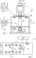
- FIG. 1 schematically depicts a lithographic apparatus LA.
- the lithographic apparatus LA includes an illumination system (also referred to as illuminator) IL configured to condition a radiation beam B (e.g., UV radiation, DUV radiation or EUV radiation), a mask support (e.g., a mask table) MT constructed to support a patterning device (e.g., a mask) MA and connected to a first positioner PM configured to accurately position the patterning device MA in accordance with certain parameters, a substrate support (e.g., a wafer table) WT constructed to hold a substrate (e.g., a resist coated wafer) W and connected to a second positioner PW configured to accurately position the substrate support in accordance with certain parameters, and a projection system (e.g., a refractive projection lens system) PS configured to project a pattern imparted to the radiation beam B by patterning device MA onto a target portion C (e.g., comprising one or more dies) of the substrate W.
- the illumination system IL receives a radiation beam from a radiation source SO, e.g. via a beam delivery system BD.
- the illumination system IL may include various types of optical components, such as refractive, reflective, magnetic, electromagnetic, electrostatic, and/or other types of optical components, or any combination thereof, for directing, shaping, and/or controlling radiation.
- the illuminator IL may be used to condition the radiation beam B to have a desired spatial and angular intensity distribution in its cross section at a plane of the patterning device MA.
- projection system PS used herein should be broadly interpreted as encompassing various types of projection system, including refractive, reflective, catadioptric, anamorphic, magnetic, electromagnetic and/or electrostatic optical systems, or any combination thereof, as appropriate for the exposure radiation being used, and/or for other factors such as the use of an immersion liquid or the use of a vacuum. Any use of the term “projection lens” herein may be considered as synonymous with the more general term “projection system” PS.
- the lithographic apparatus LA may be of a type wherein at least a portion of the substrate may be covered by a liquid having a relatively high refractive index, e.g., water, so as to fill a space between the projection system PS and the substrate W - which is also referred to as immersion lithography. More information on immersion techniques is given in US6952253 .
- the lithographic apparatus LA may also be of a type having two or more substrate supports WT (also named “dual stage”).
- the substrate supports WT may be used in parallel, and/or steps in preparation of a subsequent exposure of the substrate W may be carried out on the substrate W located on one of the substrate support WT while another substrate W on the other substrate support WT is being used for exposing a pattern on the other substrate W.
- the lithographic apparatus LA may comprise a measurement stage.
- the measurement stage is arranged to hold a sensor and/or a cleaning device.
- the sensor may be arranged to measure a property of the projection system PS or a property of the radiation beam B.
- the measurement stage may hold multiple sensors.
- the cleaning device may be arranged to clean part of the lithographic apparatus, for example a part of the projection system PS or a part of a system that provides the immersion liquid.
- the measurement stage may move beneath the projection system PS when the substrate support WT is away from the projection system PS.
- the radiation beam B is incident on the patterning device, e.g. mask, MA which is held on the mask support MT, and is patterned by the pattern (design layout) present on patterning device MA. Having traversed the mask MA, the radiation beam B passes through the projection system PS, which focuses the beam onto a target portion C of the substrate W. With the aid of the second positioner PW and a position measurement system IF, the substrate support WT can be moved accurately, e.g., so as to position different target portions C in the path of the radiation beam B at a focused and aligned position.
- the patterning device e.g. mask, MA which is held on the mask support MT, and is patterned by the pattern (design layout) present on patterning device MA.
- the radiation beam B passes through the projection system PS, which focuses the beam onto a target portion C of the substrate W.
- the substrate support WT can be moved accurately, e.g., so as to position different target portions C in the path of the radiation beam B at a focused
- first positioner PM and possibly another position sensor may be used to accurately position the patterning device MA with respect to the path of the radiation beam B.
- Patterning device MA and substrate W may be aligned using mask alignment marks M1, M2 and substrate alignment marks P1, P2.
- substrate alignment marks P1, P2 as illustrated occupy dedicated target portions, they may be located in spaces between target portions.
- Substrate alignment marks P1, P2 are known as scribe-lane alignment marks when these are located between the target portions C.
- the lithographic apparatus LA may form part of a lithographic cell LC, also sometimes referred to as a lithocell or (litho)cluster, which often also includes apparatus to perform pre- and post-exposure processes on a substrate W.
- a lithographic cell LC also sometimes referred to as a lithocell or (litho)cluster
- these include spin coaters SC to deposit resist layers, developers DE to develop exposed resist, chill plates CH and bake plates BK, e.g. for conditioning the temperature of substrates W e.g. for conditioning solvents in the resist layers.
- a substrate handler, or robot, RO picks up substrates W from input/output ports I/O1, I/O2, moves them between the different process apparatus and delivers the substrates W to the loading bay LB of the lithographic apparatus LA.
- the devices in the lithocell which are often also collectively referred to as the track, are typically under the control of a track control unit TCU that in itself may be controlled by a supervisory control system SCS, which may also control the lithographic apparatus LA, e.g. via lithography control unit LACU.
- a supervisory control system SCS which may also control the lithographic apparatus LA, e.g. via lithography control unit LACU.
- inspection tools may be included in the lithocell LC. If errors are detected, adjustments, for example, may be made to exposures of subsequent substrates or to other processing steps that are to be performed on the substrates W, especially if the inspection is done before other substrates W of the same batch or lot are still to be exposed or processed.
- An inspection apparatus which may also be referred to as a metrology apparatus, is used to determine properties of the substrates W, and in particular, how properties of different substrates W vary or how properties associated with different layers of the same substrate W vary from layer to layer.
- the inspection apparatus may alternatively be constructed to identify defects on the substrate W and may, for example, be part of the lithocell LC, or may be integrated into the lithographic apparatus LA, or may even be a stand-alone device.
- the inspection apparatus may measure the properties on a latent image (image in a resist layer after the exposure), or on a semi-latent image (image in a resist layer after a post-exposure bake step PEB), or on a developed resist image (in which the exposed or unexposed parts of the resist have been removed), or even on an etched image (after a pattern transfer step such as etching).
- the patterning process in a lithographic apparatus LA is one of the most critical steps in the processing which requires high accuracy of dimensioning and placement of structures on the substrate W.
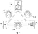
- three systems may be combined in a so called “holistic" control environment as schematically depicted in Figure 3 .
- One of these systems is the lithographic apparatus LA which is (virtually) connected to a metrology tool MT (a second system) and to a computer system CL (a third system).
- the key of such "holistic" environment is to optimize the cooperation between these three systems to enhance the overall process window and provide tight control loops to ensure that the patterning performed by the lithographic apparatus LA stays within a process window.
- the process window defines a range of process parameters (e.g. dose, focus, overlay) within which a specific manufacturing process yields a defined result (e.g. a functional semiconductor device) - typically within which the process parameters in the lithographic process or patterning process are allowed to vary.
- the computer system CL may use (part of) the design layout to be patterned to predict which resolution enhancement techniques to use and to perform computational lithography simulations and calculations to determine which mask layout and lithographic apparatus settings achieve the largest overall process window of the patterning process (depicted in Fig. 3 by the double arrow in the first scale SC1).
- the resolution enhancement techniques are arranged to match the patterning possibilities of the lithographic apparatus LA.
- the computer system CL may also be used to detect where within the process window the lithographic apparatus LA is currently operating (e.g. using input from the metrology tool MT) to predict whether defects may be present due to e.g. sub-optimal processing (depicted in Figure 3 by the arrow pointing "0" in the second scale SC2).
- the metrology tool MT may provide input to the computer system CL to enable accurate simulations and predictions, and may provide feedback to the lithographic apparatus LA to identify possible drifts, e.g. in a calibration status of the lithographic apparatus LA (depicted in Fig. 3 by the multiple arrows in the third scale SC3).
- Figure 4 depicts schematically after-develop and after-etch overlay control of a process.
- Feedback control loops run outside the lithographic apparatus.
- control loop design the following parts play a role.
- the horizontal arrows 402 represent a substrate's flow through the lithographic process. Several arrows are stacked, representing time, t.
- Exposure (EXP) 404 is followed by after-develop inspection (ADI) overlay measurements 406, 408.
- Etch (ETC) 410 is followed by after-etch inspection (AEI) overlay measurements that are dense and sparse 412, and hyper-dense 414.
- Sparse measurements 406, 412 are used to limit metrology time, with dense measurements 408, 412, 414 being performed less frequently as they require more metrology time.
- the sparse data is modeled using a certain model (consisting of different sets of parameters; for example Radial Tangential interfield parameters, hyperbolical or exponential edge model or intrafield polynomial model) that describes the process fingerprint 428 in a sufficient manner (fingerprint capture) without introducing too much noise. More parameters mean better fingerprint description, but also more noise.
- the sparse model result (process fingerprint) 428 is averaged over lots (for example using an Exponentially Weighted Moving Average) to reduce the impact of lot-to-lot variation and as such can be used, either directly or via a correction optimization step (OPT) 426, to provide stable corrections that can be applied to the exposure 404 of the next lot(s).
- lots for example using an Exponentially Weighted Moving Average
- OPT correction optimization step
- Model uncertainty is typically defined as the relative propagation of measurement error to a modelling (e.g. fitting) error when applying the model to the measurements.
- nMU normalized model uncertainty
- After-etch 412 measurements using a sparse or dense sampling layout produce sparse AEI data 422. These after-etch measurement data 422 are used to derive a global sparse model result 434.
- the global sparse model result 434 is used to apply a model offset (Metrology To Device, MTD) 432 to the after-develop data, via the ADI measurement steps 406, 408. This optional step may be done so that the control is based on reducing after-etch overlay.
- MTD Model Offset
- Dense after-develop 408 or hyper-dense after-etch 414 measurements are performed. These measurements are typically not performed for every lot, because of the additionally required metrology effort.
- the dense data 418 e.g. 2,000 point per wafer
- hyper-dense data 424 e.g. 10,000 points per wafer
- CPE Corrections Per Exposure
- a higher-order modelling is performed for this purpose to provide dense model results 436 and hyper-dense model results 438. The assumption is that the higher-order fingerprint may be more stable and as such does not have to be modeled every lot.
- the higher order model is determined on the residuals of the lower order model.
- the lower order model content can be determined on the dense data, which however may lead to a dense-to-sparse mismatch. I.e. the regular lower model determination is on sparse data which might give (only when the lower order model does not capture the fingerprint - which is typically the case) a different result then when modeling on dense data.
- the dense data may be first downsampled to determine the lower order model content.
- modelling-per-exposure is based on the residuals of the sparse subsampled data.
- the higher-order (modelling-per-exposure) ADI fingerprint 430 and higher-order (modelling-per-exposure) AEI fingerprint 438 are added (optionally after also being averaged over lots) to the lower-order fingerprint to provide a single correction set via the optimization step (OPT) 426.
- the after-etch measurements are of equal or higher density than the after-develop measurements, therefore allowing an even higher order fit.
- the dense data can be collected by means of distributed sampling. Different wafers (and different lots) have different sampling schemes so that superposing the layouts of the sampling schemes of many wafers effectively leads to a dense measurement result. In this case, no separate dense measurement is needed.
- a per-field model is used for modelling per exposure (field), which partly will pick-up the sparse-to-dense mismatch, for which it is not designed.
- a global model could be used, but then the per-field model content is missed.
- a combination is expensive in terms of metrology need and will show increased noise performance.
- Another problem is that modelling per exposure will not capture the higher order content or sparse-to-dense mismatch of each lot.
- Dense-to-sparse handling in modelling per exposure in the case of distributed sampling is not optimal except when the same wafers are measured as for the sparse measurement and when the specific sparse layout is used for mismatch handling.
- a modelling-per-exposure update will in practice not be performed on every lot - even with distributed sampling.
- Figure 5 is a flowchart of a method for determining a correction to a process according to an embodiment. The method has the steps:
- First (historical) sparse data 504 is obtained, representing measured values of a parameter across a substrate subject to the process, measured 502 using a sparse sampling layout.
- parameters are overlay, alignment, focus and dose.
- Historical dense data 512 is obtained, representing measured values of the parameter across one or more substrate subject to the process, measured 510 using a dense sampling layout that is more spatially dense than the sparse sampling layout.
- a model 508 is applied 506 to the sparse data and dense data to determine a sparse-to-dense mismatch.
- Second sparse data 522 is obtained representing measured values of the parameter across a substrate subject to the process.
- the second sparse data 522 is measured 516 using a sparse sampling layout.
- the model 508 is adapted 524 based on the sparse-to-dense mismatch. This may be done by evaluating different contributions of respective parts of the model to the sparse-to-dense mismatch. Weighting 514 factors are then determined for weighting the respective parts of the model to reduce, or preferably minimize, the sparse-to-dense mismatch.
- the model 508 is adapted with the weighting factors 514. Determining the sparse-to-dense mismatch may involve training a matrix on the first sparse data and the dense data. In that case, the step of adapting the model based on the sparse-to-dense mismatch then comprises modifying the second sparse data using the matrix.
- the adapted model is applied 524 to the second sparse data 522 to determine a sparse model result 526.
- the sparse model result 526 may be averaged 532 over several lots.
- a correction to the process is determined 542 based on the sparse model result 526.
- the correction is then applied to the process to control the process.
- the scanner setting may be adjusted based on the correction, thus controlling the lithographic process.
- After-etch inspection or electrical measurements of semiconductor devices 536 may be used to determine a metrology-to-device (MTD) model offset 540, which is applied with the determined correction 542.
- MTD metrology-to-device
- the other measurement can be taken as reference dense data 512 while the sparse overlay data 504 can itself be trained to it.
- Figure 6 is a flowchart of a method for determining a correction to a process according to another embodiment using distributed dense sampling. Features in common with those of Figure 5 have the same reference numerals. The method has the steps:
- First (historical) sparse data 504 is obtained, representing measured values of a parameter across a substrate subject to the process, measured 502 using a sparse sampling layout.
- Historical dense data 512 is obtained, representing measured values of the parameter across one or more substrate subject to the process, measured 510 using a dense sampling layout that is more spatially dense than the sparse sampling layout.
- a model 508 is applied 506 to the sparse data and dense data to determine a sparse-to-dense mismatch.
- Second sparse data 622 is obtained by downsampling 620 second dense data 618 representing measured values of the parameter across a plurality of the substrates subject to the process.
- the dense data 618 is measured 616 using different sparse sampling layouts distributed over the plurality of substrates.
- the model 508 is adapted 524 based on the sparse-to-dense mismatch. This may be done by evaluating different contributions of respective parts of the model to the sparse-to-dense mismatch. Weighting 514 factors are then determined for weighting the respective parts of the model to reduce, or preferably minimize, the sparse-to-dense mismatch.
- the model 508 is adapted with the weighting factors 514. Determining the sparse-to-dense mismatch may involve training a matrix on the first sparse data and the dense data. In that case, the step of adapting the model based on the sparse-to-dense mismatch then comprises modifying the second sparse data using the matrix.
- the adapted model is applied 524 to the second sparse data 622 to determine a sparse model result 526, 628.
- the sparse model result comprises sparse model residuals 628.
- the model 508 is applied 630 to the sparse model residuals 628 to determine a dense model result 634, which is a modelling-per-exposure fingerprint.
- the dense model result 634 may be averaged 638 over several lots.
- the sparse model result 526 may be averaged 532 over several lots.
- a correction to the process is determined 542 based on the sparse model result 526 and the dense model result 634.
- the correction is then applied to the process to control the process.
- the scanner setting may be adjusted based on the correction, thus controlling the lithographic process.
- After-etch inspection or electrical measurements of semiconductor devices 536 may be used to determine a metrology-to-device (MTD) model offset 540, which is applied with the determined correction 542.
- MTD metrology-to-device
- the other measurement can be taken as reference dense data 512 while the sparse overlay data 504 can itself be trained to it.
- a matrix may be trained on historical sparse and dense (ADI/AEI) data, the matrix mapping the sparse model parameters to modified sparse model parameters which are better suited to represent densely measured parameter data.
- ADI/AEI historical sparse and dense
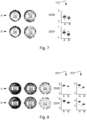
- Figure 7 depicts results of an example comparing the residual overlay performance of a dense layout for a conventional method and an embodiment.
- the sparse layout contains 200 points where the dense is ⁇ 1000 points.
- Wafer maps 702 to 710 of overlay residuals are shown. Larger residuals are depicted as longer vectors at each point on the wafer. Therefore, darker areas of the wafer maps represent worse residual overlay performance.
- A decorrected 702 and corrected 704 results are shown.
- Using a method (B) in accordance with an embodiment described with reference to Figure 5 decorrected 708 and corrected 710 results are shown.
- the box plots 712 compare mean 3-sigma overlay (overlay residual) in the x-direction (OVX) and y-direction (OVY) in nm, for the conventional method (A) and the embodiment (B).
- the embodiment (B) has lower overlay residual than the conventional method (A). This illustrates the advantage of the embodiment.
- Figure 8 depicts results of an example for distributed sampling.
- the distributed layout uses a 12-wafer cycle over 200 points in each different sparse layout to provide a dense layout ( ⁇ 2000 points).
- Wafer maps 802 to 812 of overlay residuals are shown, as for Figure 7 .
- decorrected 802 and corrected 804, 806 results are shown.
- decorrected 808 and corrected 810, 812 results are shown.
- the modeling is done in two steps; at a global level 804, 810 and from global residuals for a corrections-per-exposure (CPE) model (modelling-per-exposure level) 806, 812.
- CPE corrections-per-exposure
- the box plots 814 compare mean 3-sigma overlay (overlay residual) in the x-direction (OVX) and y-direction (OVY) in nm, for the conventional method (A) and the embodiment (B) at the global level (step 1).
- the embodiment (B) has lower overlay residual than the conventional method (A).
- the box plots 816 compare mean 3-sigma overlay (overlay residual) in the x-direction (OVX) and y-direction (OVY) in nm, for the conventional method (A) and the embodiment (B) at the modelling-per-exposure level (step 2).
- the embodiment (B) has lower overlay residual than the conventional method (A).
- the noise suppression with the embodiment (B) helps at the global level 814 already, so the cumulative effect makes the modelling-per-exposure correction even more noise-free at the modelling-per-exposure level 816.
- Embodiments may be implemented in a semiconductor manufacturing process comprising a method for determining a correction to the process according to the embodiments described herein.
- Embodiments may be implemented in a lithographic apparatus or lithographic cell as described with reference to Figures 1 and 2 .
- Embodiments may be implemented in a computer program product comprising machine readable instructions for causing a general-purpose data processing apparatus (such as LACU in Figure 2 ) to perform the steps of a method as described herein.
- a general-purpose data processing apparatus such as LACU in Figure 2
- Embodiments actively adapt the overlay model with respect to historical data, suppressing noise from it.
- Information gathering from historical dataset is used to know more about the interplay of metrology data and model/sampling.
- Two-step noise suppression in distributed sampling is also provided by embodiments.
- a per-field model is used for modelling per exposure, which partly will pick-up the sparse-to-dense mismatch, for which it is not designed.
- Embodiments reduce the noise impact for per-field model, which may result in modelling-per-exposure updates with fewer measured points.
- lithographic apparatus in the manufacture of ICs, it should be understood that the lithographic apparatus described herein may have other applications. Possible other applications include the manufacture of integrated optical systems, guidance and detection patterns for magnetic domain memories, flat-panel displays, liquidcrystal displays (LCDs), thin-film magnetic heads, etc.
- Embodiments of the invention may form part of a mask inspection apparatus, a lithographic apparatus, or any apparatus that measures or processes an object such as a wafer (or other substrate) or mask (or other patterning device).
- the term metrology apparatus or metrology system encompasses or may be substituted with the term inspection apparatus or inspection system.
- a metrology or inspection apparatus as disclosed herein may be used to detect defects on or within a substrate and/or defects of structures on a substrate.
- a characteristic of the structure on the substrate may relate to defects in the structure, the absence of a specific part of the structure, or the presence of an unwanted structure on the substrate, for example.
- the inspection or metrology apparatus that comprises an embodiment of the invention may be used to determine characteristics of physical systems such as structures on a substrate or on a wafer.
- the inspection apparatus or metrology apparatus that comprises an embodiment of the invention may be used to detect defects of a substrate or defects of structures on a substrate or on a wafer.
- a characteristic of a physical structure may relate to defects in the structure, the absence of a specific part of the structure, or the presence of an unwanted structure on the substrate or on the wafer.
- targets or target structures are metrology target structures specifically designed and formed for the purposes of measurement
- properties of interest may be measured on one or more structures which are functional parts of devices formed on the substrate.
- Many devices have regular, grating-like structures.
- the terms structure, target grating and target structure as used herein do not require that the structure has been provided specifically for the measurement being performed.
- the different product features may comprise many regions with varying sensitivities (varying pitch etc.).
- pitch p of the metrology targets is close to the resolution limit of the optical system of the scatterometer, but may be much larger than the dimension of typical product features made by lithographic process in the target portions C.
- the lines and/or spaces of the overlay gratings within the target structures may be made to include smaller structures similar in dimension to the product features.
Landscapes
- Engineering & Computer Science (AREA)
- Physics & Mathematics (AREA)
- General Physics & Mathematics (AREA)
- Manufacturing & Machinery (AREA)
- General Engineering & Computer Science (AREA)
- Automation & Control Theory (AREA)
- Artificial Intelligence (AREA)
- Quality & Reliability (AREA)
- Evolutionary Computation (AREA)
- Health & Medical Sciences (AREA)
- Software Systems (AREA)
- Theoretical Computer Science (AREA)
- Medical Informatics (AREA)
- Computer Vision & Pattern Recognition (AREA)
- Biophysics (AREA)
- Mathematical Physics (AREA)
- Computing Systems (AREA)
- Molecular Biology (AREA)
- General Health & Medical Sciences (AREA)
- Data Mining & Analysis (AREA)
- Computational Linguistics (AREA)
- Biomedical Technology (AREA)
- Life Sciences & Earth Sciences (AREA)
- Exposure And Positioning Against Photoresist Photosensitive Materials (AREA)
- Analysing Materials By The Use Of Radiation (AREA)
- Crystals, And After-Treatments Of Crystals (AREA)
- Logic Circuits (AREA)
Claims (13)
- Ein computerimplementiertes Verfahren zum Bestimmen einer Korrektur an einem Prozess, wobei das Verfahren Folgendes beinhaltet:- Erhalten erster dünnbesetzter Daten (504), die gemessene Werte eines Parameters über ein oder mehrere dem Prozess unterzogene Substrate darstellen, gemessen (502) unter Verwendung eines dünnbesetzten Stichprobenlayouts;- Erhalten dichtbesetzter Daten (512), die gemessene Werte des Parameters über ein oder mehrere dem Prozess unterzogene Substrate darstellen, gemessen (510) unter Verwendung eines dichtbesetzten Stichprobenlayouts, das räumlich dichter besetzt ist als das dünnbesetzte Stichprobenlayout;- Anwenden (506) eines Modells (508) auf die dünnbesetzten Daten und die dichtbesetzten Daten, um eine Dünn-dicht-Nichtübereinstimmung zu bestimmen;- Erhalten zweiter dünnbesetzter Daten (522; 622), die gemessene Werte des Parameters über ein dem Prozess unterzogenes Substrat darstellen, gemessen (516) unter Verwendung eines dünnbesetzten Stichprobenlayouts;- Anpassen (524) des Modells (508) auf der Basis der Dünn-dicht-Nichtübereinstimmung;- Anwenden des angepassten Modells auf die zweiten dünnbesetzten Daten, um ein dünnbesetztes Modellergebnis (526) zu bestimmen; und- Bestimmen (542) einer Korrektur an dem Prozess auf der Basis des dünnbesetzten Modellergebnisses (526).
- Verfahren gemäß Anspruch 1, wobei der Schritt des Anpassens des Models auf der Basis der Dünn-dicht-Nichtübereinstimmung Folgendes beinhaltet:- Auswerten unterschiedlicher Beiträge jeweiliger Teile des Modells zu der Dünn-dicht-Nichtübereinstimmung;- Bestimmen von Gewichtsfaktoren zum Gewichten der jeweiligen Teile des Modells, um die Dünn-dicht-Nichtübereinstimmung zu reduzieren; und- Anpassen des Modells mit den Gewichtsfaktoren.
- Verfahren gemäß Anspruch 2, wobei der Schritt des Bestimmens der Gewichtsfaktoren Folgendes beinhaltet:- Bestimmen von Gewichtsfaktoren zum Gewichten der jeweiligen Teile des Modells, um die Dünn-dicht-Nichtübereinstimmung zu minimieren.
- Verfahren gemäß einem der vorhergehenden Ansprüche, wobei das Bestimmen der Dünn-dicht-Nichtübereinstimmung das Trainieren einer Matrix an den ersten dünnbesetzten Daten und den dichtbesetzten Daten beinhaltet und der Schritt des Anpassens des Modells auf der Basis der Dünn-dicht-Nichtübereinstimmung das Modifizieren der zweiten dünnbesetzten Daten unter Verwendung der Matrix beinhaltet.
- Verfahren gemäß einem der vorhergehenden Ansprüche, wobei:- der Schritt des Erhaltens zweiter dünnbesetzter Daten das Erhalten zweiter dünnbesetzter Daten (622) durch Downsampling (620) zweiter dichtbesetzter Daten (618), die gemessene Werte des Parameters über eine Vielzahl der dem Prozess unterzogenen Substrate darstellen, beinhaltet, wobei die dichtbesetzten Daten unter Verwendung unterschiedlicher dünnbesetzter Stichprobenlayouts gemessenen werden (616), die über die Vielzahl der Substrate verteilt sind;- das dünnbesetzte Modellergebnis dünnbesetzte Modellresiduen (628) beinhaltet;- das Verfahren ferner das Anwenden (630) des Modells (508) auf die dünnbesetzten Modellresiduen (628) beinhaltet, um ein dichtbesetztes Modellergebnis (634) zu bestimmen; und- der Schritt des Bestimmens (542) einer Korrektur an dem Prozess ferner auf dem dichtbesetzten Modellergebnis (634) basiert.
- Ein Halbleiterherstellungsprozess, der ein Verfahren zum Bestimmen einer Korrektur an dem Prozess nach dem Verfahren gemäß einem der vorhergehenden Ansprüche beinhaltet.
- Ein lithographisches Gerät, das Folgendes beinhaltet:- ein Beleuchtungssystem, das konfiguriert ist, um einen Projektionsstrahl aus Strahlung bereitzustellen;- eine Trägerstruktur, die konfiguriert ist, um eine Musteraufbringungsvorrichtung zu tragen, wobei die Musteraufbringungsvorrichtung konfiguriert ist, um den Projektionsstrahl nach einem gewünschten Muster zu mustern;- einen Substrattisch, der konfiguriert ist, um ein Substrat zu halten;- ein Projektionssystem, das konfiguriert ist, um den gemusterten Strahl auf einen Zielabschnitt des Substrats zu projizieren; und- eine Verarbeitungseinheit, die konfiguriert ist, um eine Korrektur an einem Prozess nach dem Verfahren gemäß einem der Ansprüche 1 bis 5 zu bestimmen.
- Eine lithographische Zelle, die das lithographische Gerät gemäß Anspruch 7 beinhaltet.
- Ein Computerprogrammprodukt, das maschinenlesbare Anweisungen beinhaltet, um zu bewirken, dass ein Universaldatenverarbeitungsgerät Folgendes durchführt:- Erhalten erster dünnbesetzter Daten (504), die gemessene Werte eines Parameters über ein oder mehrere dem Prozess unterzogene Substrate darstellen, gemessen (502) unter Verwendung eines dünnbesetzten Stichprobenlayouts;- Erhalten dichtbesetzter Daten (512), die gemessene Werte des Parameters über ein oder mehrere dem Prozess unterzogene Substrate darstellen, gemessen (510) unter Verwendung eines dichtbesetzten Stichprobenlayouts, das räumlich dichter besetzt ist als das dünnbesetzte Stichprobenlayout;- Anwenden (506) eines Modells (508) auf die dünnbesetzten Daten und die dichtbesetzten Daten, um eine Dünn-dicht-Nichtübereinstimmung zu bestimmen;- Erhalten zweiter dünnbesetzter Daten (522; 622), die gemessene Werte des Parameters über ein dem Prozess unterzogenes Substrat darstellen, gemessen (516) unter Verwendung eines dünnbesetzten Stichprobenlayouts;- Anpassen (524) des Modells (508) auf der Basis der Dünn-dicht-Nichtübereinstimmung;- Anwenden des angepassten Modells auf die zweiten dünnbesetzten Daten, um ein dünnbesetztes Modellergebnis (526) zu bestimmen; und- Bestimmen (542) einer Korrektur an dem Prozess auf der Basis des dünnbesetzten Modellergebnisses (526).
- Computerprogrammprodukt gemäß Anspruch 9, wobei das Anpassen des Modells Folgendes beinhaltet:- Auswerten unterschiedlicher Beiträge jeweiliger Teile des Modells zu der Dünn-dicht-Nichtübereinstimmung;- Bestimmen von Gewichtsfaktoren zum Gewichten der jeweiligen Teile des Modells, um die Dünn-dicht-Nichtübereinstimmung zu reduzieren; und- Anpassen des Modells mit den Gewichtsfaktoren.
- Computerprogrammprodukt gemäß Anspruch 10, wobei das Bestimmen der Gewichtsfaktoren Folgendes beinhaltet:- Bestimmen von Gewichtsfaktoren zum Gewichten der jeweiligen Teile des Modells, um die Dünn-dicht-Nichtübereinstimmung zu minimieren.
- Computerprogrammprodukt gemäß einem der Ansprüche 9 bis 11, wobei das Bestimmen der Dünn-dicht-Nichtübereinstimmung das Trainieren einer Matrix an den ersten dünnbesetzten Daten und den dichtbesetzten Daten beinhaltet und der Schritt des Anpassens des Modells auf der Basis der Dünn-dicht-Nichtübereinstimmung das Modifizieren der zweiten dünnbesetzten Daten unter Verwendung der Matrix beinhaltet.
- Computerprogrammprodukt gemäß einem der Ansprüche 9 bis 12, wobei:- das Erhalten der zweiten dünnbesetzten Daten das Erhalten zweiter dünnbesetzter Daten (622) durch Downsampling (620) zweiter dichtbesetzter Daten (618), die gemessene Werte des Parameters über eine Vielzahl der dem Prozess unterzogenen Substrate darstellen, beinhaltet, wobei die dichtbesetzten Daten unter Verwendung unterschiedlicher dünnbesetzter Stichprobenlayouts gemessenen werden (616), die über die Vielzahl der Substrate verteilt sind;- das dünnbesetzte Modellergebnis dünnbesetzte Modellresiduen (628) beinhaltet;- das Computerprogrammprodukt ferner das Anwenden (630) des Modells (508) auf die dünnbesetzten Modellresiduen (628) durchführt, um ein dichtbesetztes Modellergebnis (634) zu bestimmen; und- das Bestimmen (542) der Korrektur an dem Prozess ferner auf dem dichtbesetzten Modellergebnis (634) basiert.
Applications Claiming Priority (6)
| Application Number | Priority Date | Filing Date | Title |
|---|---|---|---|
| EP18204882.7A EP3650939A1 (de) | 2018-11-07 | 2018-11-07 | Vorhersage eines wertes eines halbleiterherstellungsverfahrensparameters |
| EP19150953 | 2019-01-09 | ||
| EP19173992 | 2019-05-13 | ||
| EP19199505 | 2019-09-25 | ||
| EP19786562.9A EP3807720B1 (de) | 2018-11-07 | 2019-10-09 | Verfahren zum konfigurieren eines produktionsprozesses zur herstellung eines halbleiterartikels, lithographisches gerät und computerprogrammprodukt dafür |
| PCT/EP2019/077353 WO2020094325A1 (en) | 2018-11-07 | 2019-10-09 | Determining a correction to a process |
Related Parent Applications (2)
| Application Number | Title | Priority Date | Filing Date |
|---|---|---|---|
| EP19786562.9A Division EP3807720B1 (de) | 2018-11-07 | 2019-10-09 | Verfahren zum konfigurieren eines produktionsprozesses zur herstellung eines halbleiterartikels, lithographisches gerät und computerprogrammprodukt dafür |
| EP19786562.9A Division-Into EP3807720B1 (de) | 2018-11-07 | 2019-10-09 | Verfahren zum konfigurieren eines produktionsprozesses zur herstellung eines halbleiterartikels, lithographisches gerät und computerprogrammprodukt dafür |
Publications (2)
| Publication Number | Publication Date |
|---|---|
| EP3974906A1 EP3974906A1 (de) | 2022-03-30 |
| EP3974906B1 true EP3974906B1 (de) | 2025-03-26 |
Family
ID=68210809
Family Applications (2)
| Application Number | Title | Priority Date | Filing Date |
|---|---|---|---|
| EP21197330.0A Active EP3974906B1 (de) | 2018-11-07 | 2019-10-09 | Bestimmung einer korrektur an einem prozess |
| EP19786562.9A Active EP3807720B1 (de) | 2018-11-07 | 2019-10-09 | Verfahren zum konfigurieren eines produktionsprozesses zur herstellung eines halbleiterartikels, lithographisches gerät und computerprogrammprodukt dafür |
Family Applications After (1)
| Application Number | Title | Priority Date | Filing Date |
|---|---|---|---|
| EP19786562.9A Active EP3807720B1 (de) | 2018-11-07 | 2019-10-09 | Verfahren zum konfigurieren eines produktionsprozesses zur herstellung eines halbleiterartikels, lithographisches gerät und computerprogrammprodukt dafür |
Country Status (8)
| Country | Link |
|---|---|
| US (4) | US11086305B2 (de) |
| EP (2) | EP3974906B1 (de) |
| JP (2) | JP7280356B2 (de) |
| KR (3) | KR20210069104A (de) |
| CN (1) | CN112969967B (de) |
| IL (1) | IL282101B2 (de) |
| TW (4) | TWI777585B (de) |
| WO (1) | WO2020094325A1 (de) |
Families Citing this family (24)
| Publication number | Priority date | Publication date | Assignee | Title |
|---|---|---|---|---|
| CN111667111B (zh) * | 2020-06-02 | 2023-04-07 | 上海哥瑞利软件股份有限公司 | 一种集成电路晶圆制造中的良率预测方法 |
| US12287583B2 (en) | 2020-06-16 | 2025-04-29 | Asml Netherlands B.V. | Method for modeling measurement data over a substrate area and associated apparatuses |
| USD977504S1 (en) | 2020-07-22 | 2023-02-07 | Applied Materials, Inc. | Portion of a display panel with a graphical user interface |
| US11688616B2 (en) | 2020-07-22 | 2023-06-27 | Applied Materials, Inc. | Integrated substrate measurement system to improve manufacturing process performance |
| US12283503B2 (en) | 2020-07-22 | 2025-04-22 | Applied Materials, Inc. | Substrate measurement subsystem |
| US20220066411A1 (en) * | 2020-08-31 | 2022-03-03 | Applied Materials, Inc. | Detecting and correcting substrate process drift using machine learning |
| US11429091B2 (en) * | 2020-10-29 | 2022-08-30 | Kla Corporation | Method of manufacturing a semiconductor device and process control system for a semiconductor manufacturing assembly |
| TWI894386B (zh) * | 2020-11-10 | 2025-08-21 | 日商東京威力科創股份有限公司 | 模型管理系統、模型管理方法及模型管理程式 |
| EP4040233A1 (de) * | 2021-02-03 | 2022-08-10 | ASML Netherlands B.V. | Verfahren zur bestimmung eines messrezepts und zugehörige messtechnische verfahren und vorrichtungen |
| EP4050328A1 (de) * | 2021-02-25 | 2022-08-31 | ASML Netherlands B.V. | Verfahren zur vorhersage eines metrologieversatzes eines halbleiterherstellungsprozesses |
| US12450520B2 (en) * | 2021-03-01 | 2025-10-21 | Hitachi High-Tech Corporation | Experiment point recommendation device, experiment point recommendation method, and semiconductor device manufacturing device |
| EP4105719A1 (de) * | 2021-06-15 | 2022-12-21 | ASML Netherlands B.V. | Kausales faltungsnetzwerk für prozesssteuerung |
| EP4334782A1 (de) * | 2021-05-06 | 2024-03-13 | ASML Netherlands B.V. | Kausalfaltungsnetzwerk zur prozesssteuerung |
| CN113758503B (zh) * | 2021-08-12 | 2022-03-18 | 清华大学 | 一种过程参数估计方法、装置、电子设备及存储介质 |
| US12235624B2 (en) | 2021-12-21 | 2025-02-25 | Applied Materials, Inc. | Methods and mechanisms for adjusting process chamber parameters during substrate manufacturing |
| EP4216106A1 (de) * | 2022-01-19 | 2023-07-26 | ASML Netherlands B.V. | Verfahren zur steuerung eines produktionssystems und verfahren zur thermischen steuerung wenigstens eines teils einer umgebung |
| US12148647B2 (en) | 2022-01-25 | 2024-11-19 | Applied Materials, Inc. | Integrated substrate measurement system |
| US12339645B2 (en) | 2022-01-25 | 2025-06-24 | Applied Materials, Inc. | Estimation of chamber component conditions using substrate measurements |
| US12216455B2 (en) | 2022-01-25 | 2025-02-04 | Applied Materials, Inc. | Chamber component condition estimation using substrate measurements |
| US12259719B2 (en) * | 2022-05-25 | 2025-03-25 | Applied Materials, Inc. | Methods and mechanisms for preventing fluctuation in machine-learning model performance |
| KR20240001593A (ko) * | 2022-06-27 | 2024-01-03 | 주식회사 한화 | 인공 신경망을 이용하여 챔버의 상태를 예측하는 방법 및 장치 |
| US20240037442A1 (en) * | 2022-07-26 | 2024-02-01 | Applied Materials, Inc. | Generating indications of learning of models for semiconductor processing |
| US20240038558A1 (en) * | 2022-07-26 | 2024-02-01 | Kla Corporation | Metrology sampling plans for only out of specification detection |
| CN120937117A (zh) * | 2023-03-24 | 2025-11-11 | 株式会社斯库林集团 | 学习装置、信息处理装置、基板处理装置、学习方法以及处理条件决定方法 |
Family Cites Families (41)
| Publication number | Priority date | Publication date | Assignee | Title |
|---|---|---|---|---|
| JP2002134395A (ja) | 2000-10-25 | 2002-05-10 | Sony Corp | 半導体装置の製造方法および半導体装置の製造システム |
| US7006205B2 (en) | 2002-05-30 | 2006-02-28 | Applied Materials Inc. | Method and system for event detection in plasma processes |
| SG135052A1 (en) | 2002-11-12 | 2007-09-28 | Asml Netherlands Bv | Lithographic apparatus and device manufacturing method |
| JP4480482B2 (ja) | 2004-06-24 | 2010-06-16 | 株式会社日立ハイテクノロジーズ | プラズマエッチング処理装置の制御方法およびトリミング量制御システム |
| US8043797B2 (en) | 2004-10-12 | 2011-10-25 | Asml Netherlands B.V. | Lithographic apparatus and device manufacturing method |
| JP4580338B2 (ja) | 2004-12-23 | 2010-11-10 | エーエスエムエル ネザーランズ ビー.ブイ. | リソグラフィ装置、エキシマ・レーザ、およびデバイス製造方法 |
| US8175831B2 (en) * | 2007-04-23 | 2012-05-08 | Kla-Tencor Corp. | Methods and systems for creating or performing a dynamic sampling scheme for a process during which measurements are performed on wafers |
| JP2009032183A (ja) | 2007-07-30 | 2009-02-12 | Fujitsu Microelectronics Ltd | 予測装置、予測方法およびプロセス制御システム |
| US7873585B2 (en) * | 2007-08-31 | 2011-01-18 | Kla-Tencor Technologies Corporation | Apparatus and methods for predicting a semiconductor parameter across an area of a wafer |
| TWI364061B (en) * | 2008-08-20 | 2012-05-11 | Inotera Memories Inc | The method for forecasting wafer overlay error and critical dimension |
| US8078995B2 (en) * | 2009-01-06 | 2011-12-13 | International Business Machines Corporation | Efficient isotropic modeling approach to incorporate electromagnetic effects into lithographic process simulations |
| US8136054B2 (en) * | 2009-01-29 | 2012-03-13 | Synopsys, Inc. | Compact abbe's kernel generation using principal component analysis |
| NL2006024A (en) * | 2010-02-17 | 2011-08-18 | Asml Netherlands Bv | Method and apparatus for estimating model parameters of and controlling a lithographic apparatus. |
| JP2011233744A (ja) | 2010-04-28 | 2011-11-17 | Toshiba Corp | 露光方法および半導体デバイスの製造方法 |
| NL2009853A (en) | 2011-12-23 | 2013-06-26 | Asml Netherlands Bv | Methods and apparatus for measuring a property of a substrate. |
| NL2013417A (en) | 2013-10-02 | 2015-04-07 | Asml Netherlands Bv | Methods & apparatus for obtaining diagnostic information relating to an industrial process. |
| US9087176B1 (en) * | 2014-03-06 | 2015-07-21 | Kla-Tencor Corporation | Statistical overlay error prediction for feed forward and feedback correction of overlay errors, root cause analysis and process control |
| SG11201703585RA (en) | 2014-11-25 | 2017-06-29 | Kla Tencor Corp | Analyzing and utilizing landscapes |
| KR102521159B1 (ko) | 2014-11-25 | 2023-04-13 | 피디에프 솔루션즈, 인코포레이티드 | 반도체 제조 공정을 위한 개선된 공정 제어 기술 |
| KR102377411B1 (ko) | 2015-04-10 | 2022-03-21 | 에이에스엠엘 네델란즈 비.브이. | 검사와 계측을 위한 방법 및 장치 |
| US9971478B2 (en) * | 2015-04-10 | 2018-05-15 | Asml Netherlands B.V. | Method and apparatus for inspection and metrology |
| TWI737659B (zh) | 2015-12-22 | 2021-09-01 | 以色列商應用材料以色列公司 | 半導體試樣的基於深度學習之檢查的方法及其系統 |
| US10648924B2 (en) * | 2016-01-04 | 2020-05-12 | Kla-Tencor Corp. | Generating high resolution images from low resolution images for semiconductor applications |
| US10043261B2 (en) * | 2016-01-11 | 2018-08-07 | Kla-Tencor Corp. | Generating simulated output for a specimen |
| US10360477B2 (en) * | 2016-01-11 | 2019-07-23 | Kla-Tencor Corp. | Accelerating semiconductor-related computations using learning based models |
| US10181185B2 (en) * | 2016-01-11 | 2019-01-15 | Kla-Tencor Corp. | Image based specimen process control |
| US10600026B2 (en) | 2016-07-08 | 2020-03-24 | Walmart Apollo, Llc | Stocking level indication system and method |
| EP3279735A1 (de) * | 2016-08-01 | 2018-02-07 | ASML Netherlands B.V. | Messverfahren und -vorrichtung, computerprogramm und lithographisches system |
| KR101917006B1 (ko) | 2016-11-30 | 2018-11-08 | 에스케이 주식회사 | 머신 러닝 기반 반도체 제조 수율 예측 시스템 및 방법 |
| US10496781B2 (en) * | 2016-12-19 | 2019-12-03 | Kla Tencor Corporation | Metrology recipe generation using predicted metrology images |
| EP3379356A1 (de) * | 2017-03-23 | 2018-09-26 | ASML Netherlands B.V. | Verfahren zur modellierung von lithographischen systemen zur durchführung von prädiktiver wartung |
| CN107369635B (zh) * | 2017-06-06 | 2020-06-09 | 上海集成电路研发中心有限公司 | 一种基于深度学习的智能半导体装备系统 |
| JP2019007555A (ja) * | 2017-06-26 | 2019-01-17 | プラトー株式会社 | 減速機および減速機付きモータ |
| US10784174B2 (en) | 2017-10-13 | 2020-09-22 | Lam Research Corporation | Method and apparatus for determining etch process parameters |
| JP7262921B2 (ja) | 2017-11-28 | 2023-04-24 | キヤノン株式会社 | 情報処理装置、プログラム、リソグラフィ装置、リソグラフィシステム、および物品の製造方法 |
| WO2019155471A1 (en) | 2018-02-07 | 2019-08-15 | Applied Materials Israel Ltd. | Method of deep learning-based examination of a semiconductor specimen and system thereof |
| US11199506B2 (en) | 2018-02-21 | 2021-12-14 | Applied Materials Israel Ltd. | Generating a training set usable for examination of a semiconductor specimen |
| US11030557B2 (en) | 2018-06-22 | 2021-06-08 | Applied Materials, Inc. | Predicting arrival time of components based on historical receipt data |
| JP7532262B2 (ja) * | 2018-06-28 | 2024-08-13 | アプライド マテリアルズ インコーポレイテッド | 分光画像モニタリングのための機械学習システム向けのトレーニングスペクトルの生成 |
| US12067485B2 (en) * | 2018-09-28 | 2024-08-20 | Applied Materials, Inc | Long short-term memory anomaly detection for multi-sensor equipment monitoring |
| US12361531B2 (en) | 2019-05-22 | 2025-07-15 | Applied Materials Israel Ltd. | Machine learning-based classification of defects in a semiconductor specimen |
-
2019
- 2019-10-09 KR KR1020217013667A patent/KR20210069104A/ko not_active Ceased
- 2019-10-09 EP EP21197330.0A patent/EP3974906B1/de active Active
- 2019-10-09 EP EP19786562.9A patent/EP3807720B1/de active Active
- 2019-10-09 KR KR1020237029798A patent/KR102805256B1/ko active Active
- 2019-10-09 KR KR1020257014713A patent/KR102928850B1/ko active Active
- 2019-10-09 CN CN201980073186.4A patent/CN112969967B/zh active Active
- 2019-10-09 IL IL282101A patent/IL282101B2/en unknown
- 2019-10-09 JP JP2021524168A patent/JP7280356B2/ja active Active
- 2019-10-09 WO PCT/EP2019/077353 patent/WO2020094325A1/en not_active Ceased
- 2019-10-31 TW TW110119354A patent/TWI777585B/zh active
- 2019-10-31 TW TW108139392A patent/TWI703659B/zh active
- 2019-10-31 TW TW111134065A patent/TWI824707B/zh active
- 2019-10-31 TW TW109128463A patent/TWI729918B/zh active
-
2021
- 2021-02-11 US US17/174,159 patent/US11086305B2/en active Active
- 2021-07-06 US US17/367,901 patent/US11994845B2/en active Active
-
2023
- 2023-05-10 JP JP2023077714A patent/JP7542110B2/ja active Active
-
2024
- 2024-05-24 US US18/674,537 patent/US12493285B2/en active Active
-
2025
- 2025-12-08 US US19/412,585 patent/US20260111016A1/en active Pending
Also Published As
| Publication number | Publication date |
|---|---|
| TW202101633A (zh) | 2021-01-01 |
| TW202025329A (zh) | 2020-07-01 |
| CN112969967B (zh) | 2024-12-03 |
| JP2022511681A (ja) | 2022-02-01 |
| TW202135196A (zh) | 2021-09-16 |
| EP3974906A1 (de) | 2022-03-30 |
| KR20250073492A (ko) | 2025-05-27 |
| TWI824707B (zh) | 2023-12-01 |
| IL282101B2 (en) | 2023-02-01 |
| US20240345569A1 (en) | 2024-10-17 |
| EP3807720A1 (de) | 2021-04-21 |
| US11994845B2 (en) | 2024-05-28 |
| US20210165399A1 (en) | 2021-06-03 |
| JP7280356B2 (ja) | 2023-05-23 |
| US12493285B2 (en) | 2025-12-09 |
| TWI777585B (zh) | 2022-09-11 |
| KR20230130767A (ko) | 2023-09-12 |
| TWI703659B (zh) | 2020-09-01 |
| IL282101B (en) | 2022-10-01 |
| WO2020094325A1 (en) | 2020-05-14 |
| US11086305B2 (en) | 2021-08-10 |
| CN112969967A (zh) | 2021-06-15 |
| US20210333785A1 (en) | 2021-10-28 |
| KR102928850B1 (ko) | 2026-02-20 |
| KR102805256B1 (ko) | 2025-05-12 |
| EP3807720B1 (de) | 2022-05-11 |
| IL282101A (en) | 2021-05-31 |
| KR20210069104A (ko) | 2021-06-10 |
| US20260111016A1 (en) | 2026-04-23 |
| JP2023095988A (ja) | 2023-07-06 |
| TWI729918B (zh) | 2021-06-01 |
| TW202301507A (zh) | 2023-01-01 |
| JP7542110B2 (ja) | 2024-08-29 |
Similar Documents
| Publication | Publication Date | Title |
|---|---|---|
| EP3974906B1 (de) | Bestimmung einer korrektur an einem prozess | |
| US12276919B2 (en) | Method for controlling a semiconductor manufacturing process | |
| US11809088B2 (en) | Method for controlling a lithographic apparatus | |
| EP3650939A1 (de) | Vorhersage eines wertes eines halbleiterherstellungsverfahrensparameters | |
| US12416868B2 (en) | Non-correctable error in metrology | |
| US12124179B2 (en) | Method of wafer alignment using at resolution metrology on product features | |
| EP4105719A1 (de) | Kausales faltungsnetzwerk für prozesssteuerung | |
| EP3839630A1 (de) | Verfahren und vorrichtung zur konfiguration einer linsenmodellanforderung | |
| EP3786711A1 (de) | Nicht-korrigierbarer fehler in der metrologie | |
| NL2025106A (en) | Methods and apparatus for determining control data for a lithographic apparatus |
Legal Events
| Date | Code | Title | Description |
|---|---|---|---|
| PUAI | Public reference made under article 153(3) epc to a published international application that has entered the european phase |
Free format text: ORIGINAL CODE: 0009012 |
|
| STAA | Information on the status of an ep patent application or granted ep patent |
Free format text: STATUS: THE APPLICATION HAS BEEN PUBLISHED |
|
| AC | Divisional application: reference to earlier application |
Ref document number: 3807720 Country of ref document: EP Kind code of ref document: P |
|
| AK | Designated contracting states |
Kind code of ref document: A1 Designated state(s): AL AT BE BG CH CY CZ DE DK EE ES FI FR GB GR HR HU IE IS IT LI LT LU LV MC MK MT NL NO PL PT RO RS SE SI SK SM TR |
|
| STAA | Information on the status of an ep patent application or granted ep patent |
Free format text: STATUS: REQUEST FOR EXAMINATION WAS MADE |
|
| 17P | Request for examination filed |
Effective date: 20220914 |
|
| RBV | Designated contracting states (corrected) |
Designated state(s): AL AT BE BG CH CY CZ DE DK EE ES FI FR GB GR HR HU IE IS IT LI LT LU LV MC MK MT NL NO PL PT RO RS SE SI SK SM TR |
|
| P01 | Opt-out of the competence of the unified patent court (upc) registered |
Effective date: 20230414 |
|
| GRAP | Despatch of communication of intention to grant a patent |
Free format text: ORIGINAL CODE: EPIDOSNIGR1 |
|
| STAA | Information on the status of an ep patent application or granted ep patent |
Free format text: STATUS: GRANT OF PATENT IS INTENDED |
|
| INTG | Intention to grant announced |
Effective date: 20241223 |
|
| GRAS | Grant fee paid |
Free format text: ORIGINAL CODE: EPIDOSNIGR3 |
|
| GRAA | (expected) grant |
Free format text: ORIGINAL CODE: 0009210 |
|
| STAA | Information on the status of an ep patent application or granted ep patent |
Free format text: STATUS: THE PATENT HAS BEEN GRANTED |
|
| AC | Divisional application: reference to earlier application |
Ref document number: 3807720 Country of ref document: EP Kind code of ref document: P |
|
| AK | Designated contracting states |
Kind code of ref document: B1 Designated state(s): AL AT BE BG CH CY CZ DE DK EE ES FI FR GB GR HR HU IE IS IT LI LT LU LV MC MK MT NL NO PL PT RO RS SE SI SK SM TR |
|
| REG | Reference to a national code |
Ref country code: GB Ref legal event code: FG4D |
|
| REG | Reference to a national code |
Ref country code: CH Ref legal event code: EP |
|
| REG | Reference to a national code |
Ref country code: DE Ref legal event code: R096 Ref document number: 602019067973 Country of ref document: DE |
|
| REG | Reference to a national code |
Ref country code: IE Ref legal event code: FG4D |
|
| PG25 | Lapsed in a contracting state [announced via postgrant information from national office to epo] |
Ref country code: RS Free format text: LAPSE BECAUSE OF FAILURE TO SUBMIT A TRANSLATION OF THE DESCRIPTION OR TO PAY THE FEE WITHIN THE PRESCRIBED TIME-LIMIT Effective date: 20250626 |
|
| PG25 | Lapsed in a contracting state [announced via postgrant information from national office to epo] |
Ref country code: FI Free format text: LAPSE BECAUSE OF FAILURE TO SUBMIT A TRANSLATION OF THE DESCRIPTION OR TO PAY THE FEE WITHIN THE PRESCRIBED TIME-LIMIT Effective date: 20250326 |
|
| REG | Reference to a national code |
Ref country code: LT Ref legal event code: MG9D |
|
| PG25 | Lapsed in a contracting state [announced via postgrant information from national office to epo] |
Ref country code: NO Free format text: LAPSE BECAUSE OF FAILURE TO SUBMIT A TRANSLATION OF THE DESCRIPTION OR TO PAY THE FEE WITHIN THE PRESCRIBED TIME-LIMIT Effective date: 20250626 |
|
| PG25 | Lapsed in a contracting state [announced via postgrant information from national office to epo] |
Ref country code: HR Free format text: LAPSE BECAUSE OF FAILURE TO SUBMIT A TRANSLATION OF THE DESCRIPTION OR TO PAY THE FEE WITHIN THE PRESCRIBED TIME-LIMIT Effective date: 20250326 |
|
| PG25 | Lapsed in a contracting state [announced via postgrant information from national office to epo] |
Ref country code: LV Free format text: LAPSE BECAUSE OF FAILURE TO SUBMIT A TRANSLATION OF THE DESCRIPTION OR TO PAY THE FEE WITHIN THE PRESCRIBED TIME-LIMIT Effective date: 20250326 |
|
| PG25 | Lapsed in a contracting state [announced via postgrant information from national office to epo] |
Ref country code: GR Free format text: LAPSE BECAUSE OF FAILURE TO SUBMIT A TRANSLATION OF THE DESCRIPTION OR TO PAY THE FEE WITHIN THE PRESCRIBED TIME-LIMIT Effective date: 20250627 Ref country code: BG Free format text: LAPSE BECAUSE OF FAILURE TO SUBMIT A TRANSLATION OF THE DESCRIPTION OR TO PAY THE FEE WITHIN THE PRESCRIBED TIME-LIMIT Effective date: 20250326 |
|
| REG | Reference to a national code |
Ref country code: NL Ref legal event code: MP Effective date: 20250326 |
|
| PG25 | Lapsed in a contracting state [announced via postgrant information from national office to epo] |
Ref country code: NL Free format text: LAPSE BECAUSE OF FAILURE TO SUBMIT A TRANSLATION OF THE DESCRIPTION OR TO PAY THE FEE WITHIN THE PRESCRIBED TIME-LIMIT Effective date: 20250326 |
|
| PG25 | Lapsed in a contracting state [announced via postgrant information from national office to epo] |
Ref country code: SE Free format text: LAPSE BECAUSE OF FAILURE TO SUBMIT A TRANSLATION OF THE DESCRIPTION OR TO PAY THE FEE WITHIN THE PRESCRIBED TIME-LIMIT Effective date: 20250326 |
|
| REG | Reference to a national code |
Ref country code: AT Ref legal event code: MK05 Ref document number: 1779514 Country of ref document: AT Kind code of ref document: T Effective date: 20250326 |
|
| PG25 | Lapsed in a contracting state [announced via postgrant information from national office to epo] |
Ref country code: SM Free format text: LAPSE BECAUSE OF FAILURE TO SUBMIT A TRANSLATION OF THE DESCRIPTION OR TO PAY THE FEE WITHIN THE PRESCRIBED TIME-LIMIT Effective date: 20250326 |
|
| PG25 | Lapsed in a contracting state [announced via postgrant information from national office to epo] |
Ref country code: ES Free format text: LAPSE BECAUSE OF FAILURE TO SUBMIT A TRANSLATION OF THE DESCRIPTION OR TO PAY THE FEE WITHIN THE PRESCRIBED TIME-LIMIT Effective date: 20250326 Ref country code: PT Free format text: LAPSE BECAUSE OF FAILURE TO SUBMIT A TRANSLATION OF THE DESCRIPTION OR TO PAY THE FEE WITHIN THE PRESCRIBED TIME-LIMIT Effective date: 20250728 |
|
| PG25 | Lapsed in a contracting state [announced via postgrant information from national office to epo] |
Ref country code: IT Free format text: LAPSE BECAUSE OF FAILURE TO SUBMIT A TRANSLATION OF THE DESCRIPTION OR TO PAY THE FEE WITHIN THE PRESCRIBED TIME-LIMIT Effective date: 20250326 Ref country code: PL Free format text: LAPSE BECAUSE OF FAILURE TO SUBMIT A TRANSLATION OF THE DESCRIPTION OR TO PAY THE FEE WITHIN THE PRESCRIBED TIME-LIMIT Effective date: 20250326 |
|
| PG25 | Lapsed in a contracting state [announced via postgrant information from national office to epo] |
Ref country code: AT Free format text: LAPSE BECAUSE OF FAILURE TO SUBMIT A TRANSLATION OF THE DESCRIPTION OR TO PAY THE FEE WITHIN THE PRESCRIBED TIME-LIMIT Effective date: 20250326 |
|
| PG25 | Lapsed in a contracting state [announced via postgrant information from national office to epo] |
Ref country code: EE Free format text: LAPSE BECAUSE OF FAILURE TO SUBMIT A TRANSLATION OF THE DESCRIPTION OR TO PAY THE FEE WITHIN THE PRESCRIBED TIME-LIMIT Effective date: 20250326 |
|
| PG25 | Lapsed in a contracting state [announced via postgrant information from national office to epo] |
Ref country code: RO Free format text: LAPSE BECAUSE OF FAILURE TO SUBMIT A TRANSLATION OF THE DESCRIPTION OR TO PAY THE FEE WITHIN THE PRESCRIBED TIME-LIMIT Effective date: 20250326 |
|
| PG25 | Lapsed in a contracting state [announced via postgrant information from national office to epo] |
Ref country code: SK Free format text: LAPSE BECAUSE OF FAILURE TO SUBMIT A TRANSLATION OF THE DESCRIPTION OR TO PAY THE FEE WITHIN THE PRESCRIBED TIME-LIMIT Effective date: 20250326 |
|
| PG25 | Lapsed in a contracting state [announced via postgrant information from national office to epo] |
Ref country code: IS Free format text: LAPSE BECAUSE OF FAILURE TO SUBMIT A TRANSLATION OF THE DESCRIPTION OR TO PAY THE FEE WITHIN THE PRESCRIBED TIME-LIMIT Effective date: 20250726 |
|
| REG | Reference to a national code |
Ref country code: DE Ref legal event code: R097 Ref document number: 602019067973 Country of ref document: DE |
|
| PGFP | Annual fee paid to national office [announced via postgrant information from national office to epo] |
Ref country code: DE Payment date: 20251028 Year of fee payment: 7 |
|
| PG25 | Lapsed in a contracting state [announced via postgrant information from national office to epo] |
Ref country code: DK Free format text: LAPSE BECAUSE OF FAILURE TO SUBMIT A TRANSLATION OF THE DESCRIPTION OR TO PAY THE FEE WITHIN THE PRESCRIBED TIME-LIMIT Effective date: 20250326 |
|
| PG25 | Lapsed in a contracting state [announced via postgrant information from national office to epo] |
Ref country code: CZ Free format text: LAPSE BECAUSE OF FAILURE TO SUBMIT A TRANSLATION OF THE DESCRIPTION OR TO PAY THE FEE WITHIN THE PRESCRIBED TIME-LIMIT Effective date: 20250326 |
|
| PLBE | No opposition filed within time limit |
Free format text: ORIGINAL CODE: 0009261 |
|
| STAA | Information on the status of an ep patent application or granted ep patent |
Free format text: STATUS: NO OPPOSITION FILED WITHIN TIME LIMIT |
|
| REG | Reference to a national code |
Ref country code: CH Ref legal event code: L10 Free format text: ST27 STATUS EVENT CODE: U-0-0-L10-L00 (AS PROVIDED BY THE NATIONAL OFFICE) Effective date: 20260211 |
|
| 26N | No opposition filed |
Effective date: 20260105 |