EP3962070B1 - Zählerschaltung und hiermit versehener bildsensor - Google Patents
Zählerschaltung und hiermit versehener bildsensor Download PDFInfo
- Publication number
- EP3962070B1 EP3962070B1 EP21202028.3A EP21202028A EP3962070B1 EP 3962070 B1 EP3962070 B1 EP 3962070B1 EP 21202028 A EP21202028 A EP 21202028A EP 3962070 B1 EP3962070 B1 EP 3962070B1
- Authority
- EP
- European Patent Office
- Prior art keywords
- signal
- complement
- output
- reset
- counter
- Prior art date
- Legal status (The legal status is an assumption and is not a legal conclusion. Google has not performed a legal analysis and makes no representation as to the accuracy of the status listed.)
- Active
Links
Images







Classifications
-
- H—ELECTRICITY
- H03—ELECTRONIC CIRCUITRY
- H03M—CODING; DECODING; CODE CONVERSION IN GENERAL
- H03M1/00—Analogue/digital conversion; Digital/analogue conversion
- H03M1/12—Analogue/digital converters
- H03M1/14—Conversion in steps with each step involving the same or a different conversion means and delivering more than one bit
- H03M1/16—Conversion in steps with each step involving the same or a different conversion means and delivering more than one bit with scale factor modification, i.e. by changing the amplification between the steps
- H03M1/162—Conversion in steps with each step involving the same or a different conversion means and delivering more than one bit with scale factor modification, i.e. by changing the amplification between the steps the steps being performed sequentially in a single stage, i.e. recirculation type
-
- H—ELECTRICITY
- H04—ELECTRIC COMMUNICATION TECHNIQUE
- H04N—PICTORIAL COMMUNICATION, e.g. TELEVISION
- H04N25/00—Circuitry of solid-state image sensors [SSIS]; Control thereof
- H04N25/70—SSIS architectures; Circuits associated therewith
- H04N25/71—Charge-coupled device [CCD] sensors; Charge-transfer registers specially adapted for CCD sensors
- H04N25/745—Circuitry for generating timing or clock signals
-
- H—ELECTRICITY
- H03—ELECTRONIC CIRCUITRY
- H03M—CODING; DECODING; CODE CONVERSION IN GENERAL
- H03M1/00—Analogue/digital conversion; Digital/analogue conversion
- H03M1/12—Analogue/digital converters
- H03M1/1205—Multiplexed conversion systems
- H03M1/123—Simultaneous, i.e. using one converter per channel but with common control or reference circuits for multiple converters
-
- H—ELECTRICITY
- H03—ELECTRONIC CIRCUITRY
- H03M—CODING; DECODING; CODE CONVERSION IN GENERAL
- H03M1/00—Analogue/digital conversion; Digital/analogue conversion
- H03M1/12—Analogue/digital converters
- H03M1/124—Sampling or signal conditioning arrangements specially adapted for A/D converters
- H03M1/129—Means for adapting the input signal to the range the converter can handle, e.g. limiting, pre-scaling ; Out-of-range indication
- H03M1/1295—Clamping, i.e. adjusting the DC level of the input signal to a predetermined value
-
- H—ELECTRICITY
- H03—ELECTRONIC CIRCUITRY
- H03M—CODING; DECODING; CODE CONVERSION IN GENERAL
- H03M1/00—Analogue/digital conversion; Digital/analogue conversion
- H03M1/12—Analogue/digital converters
- H03M1/50—Analogue/digital converters with intermediate conversion to time interval
- H03M1/56—Input signal compared with linear ramp
-
- H—ELECTRICITY
- H04—ELECTRIC COMMUNICATION TECHNIQUE
- H04N—PICTORIAL COMMUNICATION, e.g. TELEVISION
- H04N25/00—Circuitry of solid-state image sensors [SSIS]; Control thereof
- H04N25/40—Extracting pixel data from image sensors by controlling scanning circuits, e.g. by modifying the number of pixels sampled or to be sampled
- H04N25/46—Extracting pixel data from image sensors by controlling scanning circuits, e.g. by modifying the number of pixels sampled or to be sampled by combining or binning pixels
-
- H—ELECTRICITY
- H04—ELECTRIC COMMUNICATION TECHNIQUE
- H04N—PICTORIAL COMMUNICATION, e.g. TELEVISION
- H04N25/00—Circuitry of solid-state image sensors [SSIS]; Control thereof
- H04N25/60—Noise processing, e.g. detecting, correcting, reducing or removing noise
- H04N25/616—Noise processing, e.g. detecting, correcting, reducing or removing noise involving a correlated sampling function, e.g. correlated double sampling [CDS] or triple sampling
-
- H—ELECTRICITY
- H04—ELECTRIC COMMUNICATION TECHNIQUE
- H04N—PICTORIAL COMMUNICATION, e.g. TELEVISION
- H04N25/00—Circuitry of solid-state image sensors [SSIS]; Control thereof
- H04N25/60—Noise processing, e.g. detecting, correcting, reducing or removing noise
- H04N25/618—Noise processing, e.g. detecting, correcting, reducing or removing noise for random or high-frequency noise
-
- H—ELECTRICITY
- H04—ELECTRIC COMMUNICATION TECHNIQUE
- H04N—PICTORIAL COMMUNICATION, e.g. TELEVISION
- H04N25/00—Circuitry of solid-state image sensors [SSIS]; Control thereof
- H04N25/70—SSIS architectures; Circuits associated therewith
- H04N25/71—Charge-coupled device [CCD] sensors; Charge-transfer registers specially adapted for CCD sensors
- H04N25/75—Circuitry for providing, modifying or processing image signals from the pixel array
-
- H—ELECTRICITY
- H04—ELECTRIC COMMUNICATION TECHNIQUE
- H04N—PICTORIAL COMMUNICATION, e.g. TELEVISION
- H04N25/00—Circuitry of solid-state image sensors [SSIS]; Control thereof
- H04N25/70—SSIS architectures; Circuits associated therewith
- H04N25/76—Addressed sensors, e.g. MOS or CMOS sensors
- H04N25/766—Addressed sensors, e.g. MOS or CMOS sensors comprising control or output lines used for a plurality of functions, e.g. for pixel output, driving, reset or power
-
- H—ELECTRICITY
- H04—ELECTRIC COMMUNICATION TECHNIQUE
- H04N—PICTORIAL COMMUNICATION, e.g. TELEVISION
- H04N25/00—Circuitry of solid-state image sensors [SSIS]; Control thereof
- H04N25/70—SSIS architectures; Circuits associated therewith
- H04N25/76—Addressed sensors, e.g. MOS or CMOS sensors
- H04N25/78—Readout circuits for addressed sensors, e.g. output amplifiers or A/D converters
-
- H—ELECTRICITY
- H10—SEMICONDUCTOR DEVICES; ELECTRIC SOLID-STATE DEVICES NOT OTHERWISE PROVIDED FOR
- H10F—INORGANIC SEMICONDUCTOR DEVICES SENSITIVE TO INFRARED RADIATION, LIGHT, ELECTROMAGNETIC RADIATION OF SHORTER WAVELENGTH OR CORPUSCULAR RADIATION
- H10F39/00—Integrated devices, or assemblies of multiple devices, comprising at least one element covered by group H10F30/00, e.g. radiation detectors comprising photodiode arrays
- H10F39/80—Constructional details of image sensors
- H10F39/803—Pixels having integrated switching, control, storage or amplification elements
-
- H—ELECTRICITY
- H04—ELECTRIC COMMUNICATION TECHNIQUE
- H04N—PICTORIAL COMMUNICATION, e.g. TELEVISION
- H04N25/00—Circuitry of solid-state image sensors [SSIS]; Control thereof
- H04N25/70—SSIS architectures; Circuits associated therewith
- H04N25/76—Addressed sensors, e.g. MOS or CMOS sensors
- H04N25/7795—Circuitry for generating timing or clock signals
Definitions
- Embodiments relate to a counter circuit and an image sensor including the same.
- a counter may be used to convert an effective physical quantity, such as an intensity of light, an intensity of sound, or a time, into a digital signal.
- An image sensor may obtain an image by using a characteristic of semiconductor reacting to an incident light.
- An analog-to-digital converter (“ADC") may be used to convert an analog signal output from a pixel array of the image sensor into a digital signal.
- the ADC may be implemented by using a counter that performs a counting operation based on a clock signal.
- the present invention relates to a counter circuit as defined in claim 1.
- Preferred embodiments are defined in the dependent claims.
- This disclosure is directed to an image sensor, including a pixel sensor configured to sense an incident light and to output an analog sampling signal; a sampling unit configured to compare the sampling signal and a ramp signal, and to output a comparison signal that is time-axis length information; and a counter configured to count a length of the comparison signal in response to a clock signal, a first complement control signal, and a second complement control signal.
- the counter may include a first AND gate configured to perform an AND operation on the comparison signal and the clock signal; and a first counting unit triggered at a falling edge of an output of the first AND gate to output a first count value.
- the first counting unit may include a first complement operation controller configured to store an inverted first count value corresponding to an inverted version of the first count value in response to the first complement control signal, and to output the inverted first count value in response to the second complement control signal; and a first D-flip-flop that is set or reset depending on the inverted first count value output from the first complement operation controller, and configured to output the first count value.
- a first complement operation controller configured to store an inverted first count value corresponding to an inverted version of the first count value in response to the first complement control signal, and to output the inverted first count value in response to the second complement control signal
- a first D-flip-flop that is set or reset depending on the inverted first count value output from the first complement operation controller, and configured to output the first count value.
- time-axis length information it may be meant a duration signal. That is, the comparison signal may indicate the time for which the value of the sampling signal is higher than the value of the ramp signal. In other words, the comparison signal may be considered to have a duration that is indicative of the amplitude of the sampling signal.
- This disclosure is directed to an image sensor, comprising a pixel sensor configured to sense an incident light and to output an analog sampling signal, a sampling unit configured to compare the sampling signal and a ramp signal, and to output a comparison signal having a duration that is indicative of the amplitude of the sampling signal, and a counter configured to count a length of the comparison signal in response to a clock signal, a first complement control signal, and a second complement control signal.
- the counter includes a first AND gate configured to perform an AND operation on the comparison signal and the clock signal, and a first counting unit triggered at a falling edge of an output of the first AND gate to output a first count value.
- the first counting unit includes a first complement operation controller configured to store an inverted first count value corresponding to an inverted version of the first count value in response to the first complement control signal, and to output the inverted first count value in response to the second complement control signal, and a first D-flip-flop that is set or reset depending on the inverted first count value output from the first complement operation controller, and configured to output the first count value.
- a first complement operation controller configured to store an inverted first count value corresponding to an inverted version of the first count value in response to the first complement control signal, and to output the inverted first count value in response to the second complement control signal
- a first D-flip-flop that is set or reset depending on the inverted first count value output from the first complement operation controller, and configured to output the first count value.
- the first complement operation controller may include a D-latch configured to store the inverted first count value in response to the first complement control signal, and first logic configured to transfer the inverted first count value stored in the D-latch to the first D-flip-flop in response to the second complement control signal.
- the first logic may include a second AND gate configured to perform a first AND operation on a non-inverted output signal of the D-latch and the second complement control signal, and to transfer a result of the first AND operation to a set input terminal of the D-flip-flop, and a third AND gate configured to perform a second AND operation on an inverted output signal of the D-latch and the second complement control signal, and to transfer a result of the second AND operation to a reset input terminal of the D-flip-flop.
- An inverted output signal of the first D-flip-flop may be fed back to a data input terminal of the first D-flip-flop as the inverted first count value.
- the D-latch may be configured to store the inverted first count value in response to a rising edge of the first complement control signal.
- the counter may further include a second counting unit that is triggered at a falling edge of the first count value to output a second count value being a higher bit than the first count value.
- the second counting unit may include a second complement operation controller configured to store an inverted second count value that is an inverted version of the second count value in response to the first complement control signal, and to output the inverted second count value in response to the second complement control signal, and a second D-flip-flop that is set or reset depending on the inverted second count value output from the second complement operation controller, and configured to output the second count value at a falling edge of the first count value.
- the first counting unit may further include a first multiplexer configured to select, in response to a division control signal, one of the inverted first count value and the inverted second count value to be transferred to the first complement operation controller.
- the first counting unit may be configured to store and output the inverted second count value.
- Embodiments are directed to a counter circuit that counts a high period or a low period of an input signal using a clock signal, the counter circuit including a first AND gate configured to perform an AND operation on the input signal and the clock signal; and a ripple counter triggered by an output of the first AND gate to count a length of the input signal, the ripple counter including a plurality of counting units for counting up or counting down the length of the input signal, each of the plurality of counting units including a D-latch configured to store an inverted counting bit in response to a first complement control signal; and a D-flip-flop that is set or reset by the inverted counting bit stored in the D-latch in response to a second complement control signal.
- Each of the plurality of counting units may further include a second AND gate configured to transfer a non-inverted output signal of the D-latch to a set input terminal of the D-flip-flop in synchronization with the second complement control signal.
- Each of the plurality of counting units may further include a third AND gate configured to transfer an inverted output signal of the D-latch to a reset input terminal of the D-flip-flop in synchronization with the second complement control signal.
- the ripple counter may include a first counting unit configured to toggle a least significant count value in synchronization with a falling edge of an output of the first AND gate, and a second counting unit triggered at a falling edge of an output of the first counting unit.
- An inverted output terminal of the first counting unit may be connected to a data input terminal of the first counting unit.
- the first complement control signal and the second complement control signal may be configured to sequentially transition to a high level to generate a complement of current count bits of the ripple counter.
- This disclosure is also directed to a counter circuit that counts a high period or a low period of an input signal using a clock signal, the counter circuit including a first AND gate configured to perform an AND operation on the input signal and the clock signal; and a ripple counter including a first counting unit and a second counting unit that are triggered by an output of the first AND gate to count a length of the input signal, the first counting unit toggling a first count bit, and the second counting unit toggling a second count bit that is an higher bit than the first count bit.
- the first counting unit may latch and output an inverted second count bit that is an inverted version of the second count bit toggled by the second counting unit.
- the length of the input signal may be a duration of the input signal.
- the length of the input signal may be a duration for which the input signal has a high signal level or a low signal level.
- the first counting unit may include a multiplexer configured to select one of the inverted first count bit and the inverted second count bit depending on the division control signal.
- the first counting unit may further include a complement operation controller configured to latch an output of the multiplexer in response to a first complement control signal, and to output the latched output in response to a second complement control signal.
- the first counting unit may further include a D-flip-flop that is set or reset depending on the latched output stored in the complement operation controller.
- CMOS image sensor is merely an example.
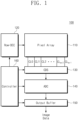
- FIG. 1 is a block diagram illustrating an image sensor according to an example.
- an image sensor 100 may include a pixel sensor array 110, a row decoder 120, a correlated double sampler (CDS) 130, an analog-to-digital converter (ADC) 140, an output buffer 150, and a controller 160.
- CDS correlated double sampler
- ADC analog-to-digital converter
- the pixel sensor array 110 may include a plurality of pixel sensors, each converting a light signal into an electrical signal, arranged two-dimensionally.
- One pixel sensor may include a single photoelectric conversion element (e.g., a photodiode).
- the pixel sensor may include at least two photoelectric conversion elements and may be driven in a reset multiple sampling scheme.
- the pixel sensor array 110 may be driven by signals that are provided from the row decoder 120, e.g., signals such as a selection signal SEL, a reset signal RS, and a transfer signal TG. Electrical signals from the pixel sensors, provided in response to the driving signals, may be provided to the CDS 130 through a plurality of column lines CL0, CL1, ..., CLm-1.
- the row decoder 120 may select a row of the pixel sensor array 110 under control of the controller 160.
- the row decoder 120 may generate the selection signal SEL for selecting one of the rows.
- the row decoder 120 may sequentially activate the reset signal RS and the transfer signal TG with regard to pixel sensors corresponding to the selected row.
- a reset signal RESET and the image signal SIG generated from each of the activated pixel sensors of the selected row in an analog shape, may be sequentially transferred to the CDS 130.
- the CDS 130 may sequentially sample and hold a set of the reset signal RESET and the image signal SIG provided from the pixel sensor array 110 to each of a plurality of column lines CL0 to CLm-1. Thus, the CDS 130 may sample and hold the levels of the reset signal RESET and the image signal SIG corresponding to each of the columns. The CDS 130 may transfer the reset signals RESET and the image signals SIG of the columns, which are sampled under control of the controller 160 in units of a plurality of columns, to the ADC 140.
- the ADC 140 may convert a sampling signal of each column output from the CDS 130 into a digital signal.
- the ADC 140 includes a counter capable of performing a complement operation and a division operation.
- the reset signal RESET and the image signal SIG may be counted by the counter using a clock signal CLK.
- a count value corresponding to the reset signal RESET may be subtracted from a count value of the image signal SIG.
- the count value corresponding to the reset signal RESET maybe converted into a negative number by the complement operation.
- image data may be generated through an addition operation.
- the counter has a circuit structure that may help reduce or eliminate coupling in the complement operation.
- image data of high reliability uninfluenced by coupling between signal lines, may be sampled by the counter.
- an image sensor using a reset multiple sampling technique may be combined with a counter having a division function to reduce noise.
- the output buffer 150 may latch and output image data provided from the ADC 140 in units of a column. Under control of the controller 160, the output buffer 150 may temporarily store image data output from the ADC 140 and may then output the sequentially latched image data.
- the output buffer 150 may be included in the image sensor 100 or may not be included in the image sensor 100.
- the controller 160 may control the pixel sensor array 110, the row decoder 120, the CDS 130, the ADC 140, and the output buffer 150.
- the controller 160 may supply control signals (e.g., a clock signal and a timing control signal) that are used for operations of the pixel sensor array 110, the row decoder 120, the CDS 130, the ADC 140, and the output buffer 150.
- the controller 160 may include a logic control circuit, a phase locked loop (PLL) circuit, a timing control circuit, a communication interface circuit, etc.
- PLL phase locked loop
- the ADC 140 includes a counter that calculates a difference value of the reset signal RESET and the image signal SIG corresponding to each column.
- the counter may further include a division function for supporting a reset multiple sampling function. Accordingly, the ADC 140 may not be influenced by coupling that causes a sensing error. Further, the image sensor 100 using the counter having the division function may use the reset multiple sampling scheme capable of reducing a noise.
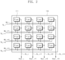
- FIG. 2 is a block diagram illustrating a pixel sensor array according to an example.
- the pixel sensor array 110 includes pixel sensors arranged in a matrix of a plurality of rows and a plurality of columns.
- Each pixel sensor 111 of the pixel sensor array 110 may include at least one of a red filter, a green filter, and a blue filter.
- the red filter transmits a light in a red wavelength band
- the green filter transmits a light in a green wavelength band
- the blue filter transmits a light in a blue wavelength band.
- the pixel sensor 111 may include a plurality of transistors and a photoelectric conversion element, and may sense light by using the photoelectric conversion element, convert the sensed light into an electrical signal, and output the electrical signal through a column line CL.
- the pixel sensor 111 may be implemented to have a structure including at least two photoelectric conversion elements.
- sampling signals Vout_j, Vout_j+1, Vout_j+2, and Vout_j+3 corresponding to the reset signal RG_i and the transfer signal TG_i may be output to column lines CL_j, CLJ+1, CL_j+2, and CL_j+3 of the selected row "i".
- the sampling signals Vout_j, Vout_j+1, Vout_j+2, and Vout_j+3 may be provided to the CDS 130 so as to be sampled as the reset signal RESET and the image signal SIG.
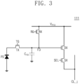
- FIG. 3 is a circuit diagram illustrating an example configuration of one pixel sensor illustrated in FIG. 2 .
- the pixel sensor 111 may include, for example, one photoelectric conversion element PD and four NMOS transistors TX, RX, DX, and SX.
- the pixel sensor 111 may further include, for example, a transistor or a capacitor for various functions.
- the photoelectric conversion element PD may be a light sensing element for generating and accumulating charges based on the amount of incident light or the intensity of light.
- the photoelectric conversion element PD may be implemented with, for example, a photo diode, a photo transistor, a photo gate, or a pinned photo diode (PPD).
- the transfer transistor TX transfers charges accumulated at the photoelectric conversion element PD to a floating diffusion area FD.
- the transfer transistor TX may be generally implemented with one transistor, turned on or off in response to the transfer signal TG_i provided from the row decoder 120.
- the floating diffusion area FD may have a function of detecting charges corresponding to the amount of incident light.
- the floating diffusion area FD integrates charges provided from the photoelectric conversion element PD while the transfer signal TG_i is activated. To accumulate charges, the floating diffusion area FD may have a capacitance C FD of a given magnitude.
- the floating diffusion area FD is connected with a gate terminal of a drive transistor DX operating as a source follower amplifier.
- the floating diffusion area FD may be provided with a power supply voltage VDD by the reset transistor RX.
- the reset transistor RX resets the floating diffusion area FD in response to the reset signal RG_i.
- a source of the reset transistor RX is connected to the floating diffusion area FD, and a drain thereof is connected to a power supply voltage (VDD) terminal.
- VDD power supply voltage
- the reset transistor RX is turned on by a bias voltage of the reset signal RG_i, the power supply voltage VDD connected with the drain of the reset transistor RX is transferred to the floating diffusion area FD.
- the charges accumulated at the floating diffusion area FD move to the power supply voltage (VDD) terminal, and a voltage of the floating diffusion area FD is reset.
- the drive transistor DX operates as a source follower amplifier, amplifies the change in an electrical potential of the floating diffusion area FD, and outputs a result of the amplification as the sense voltage Vout_j.
- the selection transistor SX selects a pixel sensor to be read in units of a row.
- the selection transistor SX is driven by the selection signal SEL provided in units of a row.
- the selection transistor SX is turned on, the potential of the floating diffusion area FD may be amplified through the drive transistor DX and may then be transferred to a drain of the selection transistor SX.
- Driving signal lines TG_i, RG_i, and SEL of the transfer transistor TX, the reset transistor RX, and the selection transistor SX extend in a row direction (e.g., a horizontal direction) such that each of the pixel sensors included in the same row are simultaneously driven.
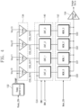
- FIG. 4 is a block diagram illustrating an example structure of a correlated double sampler, an analog-to-digital converter, and an output buffer of FIG. 1 .
- the CDS 130 may include a ramp signal generator 132 and comparators 134.
- the ADC 140 may include a plurality of counters CNT_0, CNT_1, CNT_2, and CNT_3.
- the output buffer 150 may include memories MEM_0, MEM_1, MEM_2, and MEM_3, and a sense amplifier 154. The output buffer 150 may be included in the image sensor 100 or may not be included in the image sensor 100.
- the ramp signal generator 132 of the CDS 130 outputs a ramp signal RAMP having a uniform falling or rising slope in response to a control signal Ramp_EN from the controller 160.
- the ramp signal generator 132 continuously generates the ramp signal RAMP having a particular slope under control of the controller 160.
- each of the reset signal RESET and the image signal SIG is converted into time-axis length information. That is, signals having a duration that corresponds to the amplitude of each of the reset signal RESET and the image signal SIG are generated.
- the comparators 134 may include a plurality of comparators Comp0, Comp1, Comp2, and Comp3 corresponding to respective columns of the pixel sensor array 110.
- the comparators 134 compare sampling signals Vout0, Vout1, Vout2, and Vout3 respectively corresponding to columns with the ramp signal RAMP.
- Each of the sampling signals Vout0, Vout1, Vout2, and Vout3 includes the reset signal RESET and the image signal SIG that are sampled and held by a correlated double sampling operation. That is, depending on the phase of operation, the sampling signals Vout0, Vout1, Vout2, and Vout3 may have a value which represent a reset signal RESET or an image signal SIG of a corresponding pixel sensor.
- the ramp signal RAMP is input to an inverting input terminal (-) of the first comparator Comp0, and the sampling signal Vout0 is input to a non-inverting input terminal (+) of the first comparator CompO.
- the first comparator CompO may output a CDS output signal CDS_OUT0 by comparing the ramp signal RAMP and the reset signal RESET of the sampling signal Vout0 in a first period and comparing the ramp signal RAMP and the image signal SIG of the sampling signal Vout0 in a second period. Through this procedure, the reset signal RESET and the image signal SIG including level information may be converted into time-axis length information.
- the ADC 140 includes counters CNT_0, CNT_1, CNT_2, and CNT_3 that are provided with the clock signal CLK and complement control signals BWI and BWI_C from the controller 160.
- the counters CNT_0 to CNT_3 may count CDS output signals CDS_OUT0 to CDS_OUT3 of the comparators 134 corresponding to the time-axis length information and may convert count values to digital information.
- the counters CNT_0 to CNT_3 may perform a stable complement operation on a count value even under the condition that the complement control signals BWI and BWI_C are unstable due to the coupling.
- a structure and an operation of the counters CNT_0 to CNT_3 will be more fully described with reference to FIGS. 5 to 8 .
- the output buffer 150 may include a column memory 152 and the sense amplifier 154.
- the column memory 152 may store image data corresponding to each column in response to a control signal Mem_EN from the controller 160.
- the column memory 152 may include the plurality of memories MEM_0, MEM_1, MEM_2, and MEM_3, each of which transfers image data stored therein to the sense amplifier 154.
- the output buffer 150 may be included in the image sensor 100 (refer to FIG. 1 ) or may not be included in the image sensor 100.
- the structure of the ADC 140 including the counters CNT_0, CNT_1, CNT_2, and CNT_3 according to an example is described above.
- Each of the counters CNT_0, CNT_1, CNT_2, and CNT_3 according to an example may be able to perform a stable complement operation even in the condition that the complement control signals BWI and BWI_C are unstable due to the coupling.
- FIG. 5 is a circuit diagram illustrating a counter according to an example.
- FIG. 5 An example structure of the counter CNT_0 of the counters CNT_0 to CNT_3 of FIG. 4 is illustrated in FIG. 5 .
- Structures of the counters CNT_1, CNT_2, and CNT_3 may be identical to the structure of the counter CNT_0.
- the counter CNT_0 may include an AND gate 141 and a plurality of counting units 142, 143, 144, and 145.
- the counter CNT_0 may be implemented as an asynchronous ripple counter in which one counting unit 142 is triggered by the clock signal CLK.
- the AND gate 141 transfers the clock signal CLK to a "CLK" input terminal of the first counting unit 142 only in a high-level period of the CDS output signal CDS_OUT0.
- the first counting unit 142 includes a D-flip-flop that is triggered at a falling edge of a signal provided to the "CLK" input terminal basically.
- signals of output terminals Q and /Q are toggled at a falling edge of an input clock of the first counting unit 142.
- the inverted output terminal /Q is connected to a data input terminal "D" of the first counting unit 142.
- an output of the first counting unit 142 outputs a least significant bit Q ⁇ 0> that repeatedly toggles in synchronization with the falling edge of the input clock.
- the first counting unit 142 may invert and output the latched data in response to the complement control signals BWI and BWI_C.
- Functions of the second to fourth counting units 143 to 145 are substantially identical to the function of the first counting unit 142.
- the counter CNT_0 counts the reset signal RESET that is provided as the CDS output signal CDS_OUT0.
- a count value of the reset signal RESET may be inverted and converted into a ones' complement value.
- the complement value may be used as a negative number in a binary operation.
- an image data value (SIG - RESET) that corresponds to a result of subtracting the reset signal RESET from the image signal SIG may be obtained from the counter CNT_0 by counting up the image signal SIG based on the inverted count value of the reset signal RESET. That is, by counting up the image signal SIG starting at the inverted count value of the reset signal RESET the image value SIG may be added to the inverted reset signal RESET to generate an image data value (SIG - RESET).
- the counter CNT_0 may perform a stable count operation by using the D-flip-flop (or D-latch) even if the complement control signals BWI and BWI_C fluctuate due to the coupling. This will be described in further detail below.
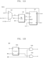
- FIGS. 6A and 6B are block diagrams illustrating a structure of a counting unit of FIG. 5 .
- a counting unit CU ⁇ k> (which corresponds to one of the counting units CU ⁇ 0> to CU ⁇ n-1> constituting the counter CNT_0) includes a complement operation controller 146 and a D-flip-flop 147.
- the complement operation controller 146 may be implemented by using AND gates 146b and 146c and a D-latch 146a.
- FIG. 6A will be described in detail below.
- the complement operation controller 146 of the counting unit CU ⁇ k> is provided with an inverted output /Q ⁇ k> of the counting unit CU ⁇ k> and the complement control signals BWI and BWI_C.
- the inverted output /Q ⁇ k> of the counting unit CU ⁇ k> is fed back to the complement operation controller 146 and an input terminal "D" of the D-flip-flop 147.
- the complement operation controller 146 stores the fed-back inverted output /Q ⁇ k> by using the D-latch 146a (refer to FIG. 6B ). Accordingly, even if a level of the inverted output /Q ⁇ k> is unstable, a value of the first latched inverted output /Q ⁇ k> may be maintained.
- the inverted output /Q ⁇ k> maintained by the complement operation controller 146, and signals derived from the inverted output /Q ⁇ k> are provided to a "SET" terminal and a "RESET” terminal of the D-flip-flop 147. Accordingly, even if the inverted output /Q ⁇ k> provided to the data input terminal "D" of the D-flip-flop 147 is unstable, a value of an output terminal "Q" of the D-flip-flop 147 may change depending on states of the "SET” terminal and the "RESET” terminal of the D-flip-flop 147.
- An output value Q ⁇ k-1> of a lower counting unit CU ⁇ k-1> is provided to a "CLK" input terminal of the D-flip-flop 147. The D-flip-flop 147 is triggered at a falling edge of the output value Q ⁇ k-1> of the counting unit CU ⁇ k-1>.
- FIG. 6B will be described in detail below.
- the complement operation controller 146 may include the D-latch 146a and the AND gates 146b and 146c.
- the fed-back inverted signal /Q ⁇ k> is input to a data input terminal "D" of the D-latch 146a, and the first complement control signal BWI_C is input to a clock input terminal of the D-latch 146a.
- the fed-back inverted signal /Q ⁇ k> is stored in the D-latch 146a in synchronization with a rising edge of the first complement control signal BWI_C.
- a bit value of the inverted output /Q ⁇ k> may be stably maintained by the D-latch 146a until a next rising edge of the first complement control signal BWI_C.
- the bit value of the inverted output /Q ⁇ k> that is stored in the D-latch 146a at the rising edge of the first complement control signal BWI_C is output to the D-flip-flop 147 in response to the second complement control signal BWI.
- the AND gate 146b receives a non-inverted output "Q" of the D-latch 146a and the second complement control signal BWI and outputs a set signal "S”.
- the AND gate 146c receives an inverted output /Q of the D-latch 146a and the second complement control signal BWI and outputs a reset signal "R".
- the bit value stored in the D-latch 146a may be transferred to the "SET" terminal or the "RESET" terminal of the D-flip-flop 147 through the AND gates 146b and 146c depending on the second complement control signal BWI.
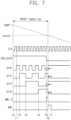
- FIG. 7 is a timing diagram briefly illustrating a complement operation of a counter illustrated in FIG. 5 .
- the counter CNT_0 may invert a count value so as to be converted into the ones' complement.
- the complement control signals BWI_C and BWI maintain a low level until a time T5.
- the sampling signal Vout0 may be maintained at a fixed value, and the ramp signal RAMP may fall with a given slope over time. A counting operation of the counter CNT_0 starts.
- the CDS output signal CDS_OUT0 which is a result of comparing the ramp signal RAMP and the sampling signal Vout0, appears at high level.
- the clock signal CLK is transferred to the first counting unit CU ⁇ 0> through the AND gate 141.
- the first counting unit CU ⁇ 0> is triggered at a falling edge of the clock signal CLK. Accordingly, a least significant bit Q ⁇ 0> is toggled to logic '1' at a time T1 corresponding to a first falling edge of the clock signal CLK, and is again toggled to logic '0' at a time T2 corresponding to a second falling edge of the clock signal CLK.
- the toggling operation of the first counting unit CU ⁇ 0> may be performed while the clock signal CLK is provided to the first counting unit CU ⁇ 0>.
- the toggling operation of the first counting unit CU ⁇ 0> is performed in a period where the CDS output signal CDS_OUT0 is maintained at the high level.
- the output bit value Q ⁇ 0> of the first counting unit CU ⁇ 0> has a high-to-low transition.
- the second counting unit CU ⁇ 1> is triggered by the high-to-low transition of the output bit value Q ⁇ 0> and starts to be toggled.
- a bit value Q ⁇ 1> is toggled to logic ' 1' at the time T2 when the output bit value Q ⁇ 0> has the high-to-low transition.
- the bit value Q ⁇ 1> is again toggled to logic '0' at a time T3 when the output bit value Q ⁇ 0> has a second high-to-low transition.
- the toggling operation of the second counting unit CU ⁇ 1> may be performed while the CDS output signal CDS_OUT0 is maintained at the high level.
- the output bit value Q ⁇ 1> of the second counting unit CU ⁇ 1> has a high-to-low transition. Accordingly, the third counting unit CU ⁇ 2> is triggered by the high-to-low transition of the output bit value Q ⁇ 1> and starts to be toggled. Thus, a bit value Q ⁇ 2> is toggled to logic ' 1' at the time T3 when the output bit value Q ⁇ 1> has the high-to-low transition. The bit value Q ⁇ 2> is again toggled to logic '0' at a time T4 when the output bit value Q ⁇ 1>has second high-to-low transition. The toggling operation of the third counting unit CU ⁇ 2> may be performed while the CDS output signal CDS_OUT0 is maintained at the high level.
- the output bit value Q ⁇ 2> of the third counting unit CU ⁇ 2> has a high-to-low transition.
- the fourth counting unit CU ⁇ 3> is triggered by the high-to-low transition of the output bit value Q ⁇ 2> and starts to be toggled.
- a bit value Q ⁇ 3> is toggled to logic '1' at the time T4 when the output bit value Q ⁇ 2> has the high-to-low transition.
- the bit value Q ⁇ 3> is again toggled to logic '0' at a time the output bit value Q ⁇ 2> has a second high-to-low transition.
- the CDS output signal CDS_OUT0 transitions to the low level.
- the transfer of the clock signal CLK to the first counting unit CU ⁇ 0> may be blocked, and the counting operation may be interrupted.
- a count value of the counter CNT_0 is "1010"(Q ⁇ 3>, Q ⁇ 2>, Q ⁇ 1>, Q ⁇ 0>).
- an inverted output value of each of the counting units CU ⁇ 0>, CU ⁇ 1>, CU ⁇ 2>, and CU ⁇ 3> is stored in the D-latch 146a (refer to FIG. 6A ) included in the complement operation controller 146.
- the inverted output value of each of the counting units CU ⁇ 0>, CU ⁇ 2>, CU ⁇ 2>, and CU ⁇ 3> is provided to the "SET" terminal of the D-flip-flop 147, with an opposite value being provided to the "RESET” terminal of the D-flip-flop 147 (refer to FIG. 6A and 6B ).
- the count value of the counter CNT_0 that is, "1010” is converted into the ones' complement, that is, "0101”.
- the counter CNT_0 may maintain the ones' complement thus obtained, that is, "0101".
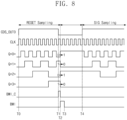
- FIG. 8 is a timing diagram illustrating an operation of a counter according to an example for correlated double sampling
- a counter may sample the reset signal RESET to obtain the complement, and may then process a correlated double sampling signal to sample the image signal SIG.
- the sampling signal Vout0 corresponding to the reset signal RESET may be transferred to the comparator CompO.
- the CDS output signal CDS_OUT0 transitions to the high level.
- the clock signal CLK is transferred to the first counting unit CU ⁇ 0> through the AND gate 141. Afterwards, a high-level period of the CDS output signal CDS_OUT0 is counted by the counting units CU ⁇ 0>, CU ⁇ 1>, CU ⁇ 2>, and CU ⁇ 3>.
- the CDS output signal CDS_OUT0 transitions to the low level.
- the transfer of the clock signal CLK to the first counting unit CU ⁇ 0> may be blocked, and the counting operation of the counter CNT_0 may be interrupted.
- a count value of the counter CNT_0 is "1010"(Q ⁇ 3>, Q ⁇ 2>, Q ⁇ 1>, Q ⁇ 0>).
- an inverted output value of each of the counting units CU ⁇ 0>, CU ⁇ 1>, CU ⁇ 2>, and CU ⁇ 3> is stored in the D-latch 146a (refer to FIG. 6B ).
- the inverted output value stored in the D-latch 146a of each of the counting units CU ⁇ 0>, CU ⁇ 2>, CU ⁇ 2>, and CU ⁇ 3> is transferred to the D-flip-flop 147 (refer to FIG. 6A ).
- the count value of the counter CNT_0 that is, "1010” is converted into the ones' complement, that is, "0101".
- the counter CNT_0 may maintain the ones' complement of the count value thus obtained, that is, "0101".
- the sampling signal Vout0 corresponding to the image signal SIG may be transferred to the comparator CompO.
- the CDS output signal CDS_OUT0 transitions to the high level.
- the clock signal CLK is transferred to the first counting unit CU ⁇ 0> through the AND gate 141. Afterwards, a high-level period of the CDS output signal CDS_OUT0 is counted by the counting units CU ⁇ 0>, CU ⁇ 1>, CU ⁇ 2>, and CU ⁇ 3>.
- a count start value of the counter CNT_0 may be "0101" being the ones' complement of the count value of the reset signal RESET.
- the counter CNT_0 operates to add the count value of the image signal SIG to "0101" corresponding to a negative number. Accordingly, the count value corresponding to the reset signal RESET may be subtracted from the count value of the image signal SIG.
- a correlated double sampling value may be easily converted into digital data without a separate memory for storing the count value of the reset signal RESET.
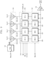
- FIG. 9 is a block diagram illustrating an example structure of a correlated double sampler, an analog-to-digital converter, and an output buffer of FIG. 1 , according to another example.
- the CDS 130 may include the ramp signal generator 132 and the comparators 134.
- An analog-to-digital converter 240 may include the plurality of counters CNT_0, CNT_1, and CNT_2, CNT_3.
- the output buffer 150 may include the memories MEM_0, MEM_1, MEM_2, and MEM_3, and the sense amplifier 154.
- the CDS 130 and the output buffer 150 may be identical to those of FIG. 4 , and thus, additional description will be omitted to avoid redundancy.
- the analog-to-digital converter 240 includes the counters CNT_0, CNT_1, CNT_2, and CNT_3 that are provided with the clock signal CLK, the complement control signals BWI and BWI_C, and a division control signal DIVIDE.
- the counters CNT_0 to CNT_3 may count the CDS output signals CDS_OUT0 to CDS_OUT3 of the comparators 134 corresponding to the time-axis length information, and may convert the count results to digital information.
- the counters CNT_0 to CNT_3 may perform a stable complement operation on the count values even if complement control signals BWI and BWI_C are unstable due to the coupling.
- the counters CNT_0 to CNT_3 may divide a binary count value by "2" in response to the division control signal DIVIDE. A structure and an operation of the counters CNT_0 to CNT_3 will be more fully described below.
- the structure of the analog-to-digital converter 240 including the counters CNT_0, CNT_1, CNT_2, and CNT_3 including the complement function and the division function according to an example is described above.
- Each of the counters CNT_0, CNT_1, CNT_2, and CNT_3 according to an example may be able to perform a stable complement operation even if the complement control signals BWI and BWI_C are unstable due to the coupling.
- the analog-to-digital converter 240 may easily adopt a reset multiple sampling technique, and may reduce a magnitude of a noise.
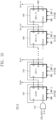
- FIG. 10 is a circuit diagram illustrating a counter according to another example.
- FIG. 10 An example structure of the counter CNT_0 of the counters CNT_0 to CNT_3 of FIG. 9 is illustrated in FIG. 10 . Structures of the remaining counters CNT_1, CNT_2, and CNT_3 may be identical to the structure of the counter CNT_0.
- the counter CNT_0 may include an AND gate 241, and a plurality of counting units 242, 243, 244, and 245.
- the counter CNT_0 may be implemented with an asynchronous ripple counter in which one counting unit 242 is triggered by the clock signal CLK.
- the AND gate 241 transfers the clock signal CLK to a clock input terminal of the first counting unit 242 only in a high-level period of the CDS output signal CDS_OUT0.
- the first counting unit 242 includes a D-flip-flop that is triggered at a falling edge. Thus, signals of output terminals Q and /Q are toggled at a falling edge of an input clock of the first counting unit 242.
- the inverted output terminal /Q is connected to a data input terminal "D" of the first counting unit 242. Accordingly, the first counting unit 242 outputs a least significant bit Q ⁇ 0> that is repeatedly toggled in synchronization with a falling edge of the input clock.
- the first counting unit 242 may invert and output the latched data in response to the complement control signals BWI and BWI_C.
- the first counting unit 242 may perform a division operation of dividing the latched binary data by "2" in response to the division control signal DIVIDE. Functions of the second to fourth counting units 243 to 245 are substantially identical to the function of the first counting unit 242.
- the counter CNT_0 may perform a multiple sampling operation of sampling the image signal SIG and the reset signal RESET a plurality of times and outputting an average value.
- output image data may be "(SIG- (REF1 + REF2)/2".
- a reset noise may decrease as much as 1/root(2) times, thus implementing a low-noise image sensor.
- the division function may divide a count value by "2" for calculating an average value.
- the counters CNT_0, CNT_1, CNT_2, and CNT_3 included in the analog-to-digital converter 240 may divide a count value in response to the division control signal DIVIDE.
- FIGS. 11A and 11B are block diagrams illustrating a structure of a counting unit of FIG. 10 .
- a counting unit CU ⁇ k> that corresponds to one of the counting units CU ⁇ 0> to CU ⁇ n-1> constituting the counter CNT_0 includes a multiplexer 248, a complement operation controller 246, and a D-flip-flop 247.
- the complement operation controller 246 may be implemented by using AND gates 246b and 246c and a D-latch 246a.
- FIG. 11A will be described in detail below.
- a data signal Qi which is selected by the multiplexer 248, is provided to an input terminal "D" of the complement operation controller 246.
- the multiplexer 248 selects the inverted output /Q ⁇ k> of the counting unit CU ⁇ k>.
- the inverted output /Q ⁇ k> is provided to the input terminal "D" of the complement operation controller 246, the complement operation controller 246 and the D-flip-flop 247 may perform the same complement operation as the counting unit CU ⁇ k> of FIG. 6A .
- the complement operation controller 246 is provided with the fed-back inverted output /Q ⁇ k> of the counting unit CU ⁇ k> and the complement control signals BWI and BWI_C.
- the inverted output /Q ⁇ k> is fed back to the complement operation controller 246 and an input terminal "D" of the D-flip-flop 247.
- the complement operation controller 246 stores the fed-back inverted output /Q ⁇ k> using the D-latch 146a (refer to FIG. 11B ). Accordingly, even if a level of the inverted output /Q ⁇ k> is unstable, a value of the latched inverted output /Q ⁇ k> may be maintained.
- the inverted output /Q ⁇ k> maintained by the complement operation controller 246 is provided to a "SET" terminal of the D-flip-flop 247, and an opposite signal generated by the complement operation controller 246 is provided to a "RESET” terminal of the D-flip-flop 247. Accordingly, even if the inverted output /Q ⁇ k> provided to a data input terminal "D" of the D-flip-flop 247 is unstable, a value of an output terminal "Q" of the D-flip-flop 247 may change depending on states of the "SET” terminal and the "RESET” terminal of the D-flip-flop 147.
- a non-inverted output Q ⁇ k-1> of a lower counting unit CU ⁇ k-1> is provided to a "CLK" input terminal of the D-flip-flop 247.
- the D-flip-flop 247 is triggered at a falling edge of the non-inverted output Q ⁇ k-1>.
- the multiplexer 248 selects the inverted output /Q ⁇ k+1> of the counting unit CU ⁇ k+1> corresponding to an higher count value Qu.
- the complement operation controller 246 and the D-flip-flop 247 may perform an operation of latching the higher count value Qu.
- a shift to a lower bit corresponds to an operation of dividing a count value by "2".
- the complement operation and the division operation are performed through the D-flip-flops 247 by shifting the inverted count value /Q ⁇ k+1> of the higher counting unit CU ⁇ k+1> to the lower counting unit CU ⁇ k>.
- the complement operation controller 246 may include the D-latch 246a and the AND gates 246b and 246c.
- the fed-back inverted signal /Q ⁇ k> is input to a data input terminal "D" of the D-latch 246a (when the DIVIDE signal is '0', meaning that the inverted signal /Q ⁇ k> is provided as the input data Qi), and the first complement control signal BWI_C is input to a clock input terminal of the D-latch 246a.
- the inverted output /Q ⁇ k> is stored in the D-latch 246a in synchronization with a rising edge of the first complement control signal BWI_C.
- a bit value of the inverted output /Q ⁇ k> may be stably maintained by the D-latch 246a until a next rising edge of the first complement control signal BWI_C.
- the bit value of the inverted output /Q ⁇ k> that is stored in the D-latch 246a at the rising edge of the first complement control signal BWI_C is output to the D-flip-flop 247 in response to the second complement control signal BWI.
- the AND gate 246b receives a non-inverted output "Q" of the D-latch 246a and the second complement control signal BWI and outputs a set signal "S”.
- the AND gate 246c receives an inverted output /Q of the D-latch 246a and the second complement control signal BWI and outputs a reset signal "R".
- the bit value stored in the D-latch 246a may be transferred to the "SET” and "RESET" terminals of the D-flip-flop 247 through the AND gates 246b and 246c depending on the second complement control signal BWI.
- the complement operation controller 246 may selectively perform the division operation or the complement operation depending on the input data Qi.
- FIG. 12 is a timing diagram illustrating a division operation performed by a counter of FIG. 10 .
- the counter CNT_0 in response to the complement control signals BWI_C and BWI and the division control signal DIVIDE, the counter CNT_0 may invert a count value or may perform a division operation on the count value.
- the CDS output signal CDS_OUT0 which is a result of comparing the ramp signal RAMP and the sampling signal Vout0, transitions to the high level.
- the clock signal CLK is transferred to the first counting unit CU ⁇ 0> through the AND gate 241 (refer to FIG. 10 ).
- the first counting unit CU ⁇ 0> is triggered at a falling edge of the clock signal CLK. Accordingly, the counting operation of the counter CNT_0 may start from a time when the clock signal CLK transitions to the low level.
- count values Q ⁇ 0>, Q ⁇ 1>, Q ⁇ 2>, and Q ⁇ 3> of the counting units CU ⁇ 0>, CU ⁇ 1>, CU ⁇ 2>, and CU ⁇ 3> are counted up.
- the CDS output signal CDS_OUT0 transitions to the low level, and the division control signal DIVIDE transitions to the high level.
- the transfer of the clock signal CLK may be blocked, and the counting operation of the counter CNT_0 may be interrupted.
- a count value of the counter CNT_0 is "1010"(Q ⁇ 3>, Q ⁇ 2>, Q ⁇ 1>, Q ⁇ 0>).
- an inverted output value of each of the counting units CU ⁇ 0>, CU ⁇ 1>, CU ⁇ 2>, and CU ⁇ 3> is stored in the D-latch 246a (refer to FIG. 11A ).
- the multiplexer 248 (refer to FIG. 11A ) of each of the counting units CU ⁇ k> may select the inverted count value /Q ⁇ k+1> of the counting unit CU ⁇ k+1> corresponding to the higher count value Qu.
- the inverted output value of each of the counting units CU ⁇ 0>, CU ⁇ 1>, CU ⁇ 2>, and CU ⁇ 3> is provided to the "SET" terminal of the D-flip-flop 247 (refer to FIG. 11A ), with an opposite signal being provided to the "RESET” terminal of the D-flip-flop 247.
- the count value of the counter CNT_0, that is, "1010” is converted into the ones' complement, that is, "0101".
- the multiplexer 248 selects the inverted output /Q ⁇ k+1> of the counting unit CU ⁇ k+1> corresponding to the higher count value Qu.
- the complement operation controller 246 and the D-flip-flop 247 may perform an operation of latching the higher count value Qu. Accordingly, the counting units CU ⁇ 0>, CU ⁇ 1>, CU ⁇ 2>, and CU ⁇ 3> perform a shift operation on "0101" being the ones' complement, such that a higher bit is shifted to a lower bit.
- a least significant bit '1' of "0101" being the ones' complement may be invalidated, and the remaining three bits “010" may be maintained at the counter CNT_0.
- This operation corresponds to the division operation of dividing the reset signal RESET converted into a negative number through the complement operation, by "2".
- the second complement control signal BWI transitions to the low level at a time T3
- the division control signal DIVIDE transitions to the low level at a time T4.
- the counter CNT_0 may maintain the divided ones' complement thus obtained, that is, "010" as the count value.
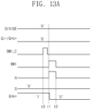
- FIGS. 13A and 13B are timing diagrams illustrating operations of the counting unit CU ⁇ k> performing only a complement operation.
- FIG. 13A illustrates the complement operation in the case where a current data value Q ⁇ k> of the counting unit CU ⁇ k> is logic '1'
- FIG. 13B illustrates the complement operation in the case where the current data value Q ⁇ k> of the counting unit CU ⁇ k> is logic '0'.
- the current data value Q ⁇ k> of the counting unit CU ⁇ k> is logic '1', and the division control signal DIVIDE maintains the low level '0'.
- the first complement control signal BWI_C transitions to the high level.
- Logic '0' corresponding to the input Qi is stored in the D-latch 246a (refer to fig. 11B ) in the complement operation controller 246 (refer to FIG. 11B ) in synchronization with a rising edge of the first complement control signal BWI_C.
- the second complement control signal BWI transitions to the high level.
- the output value Q ⁇ k> of the D-flip-flop 247 may transition to a reset value, that is, logic '0'.
- the division control signal DIVIDE is at the low level ('0'), and the current data value Q ⁇ k> of the counting unit CU ⁇ k> is logic '0'.
- logic '1' is stored in the D-latch 246a (refer to fig. 11B ) of the complement operation controller 246 (refer to FIG. 11B ).
- the first complement control signal BWI_C transitions to the high level.
- Logic '1' corresponding to the input Qi is stored in the D-latch 246a (refer to fig. 11B ) of the complement operation controller 246 (refer to FIG. 11B ) in synchronization with a rising edge of the first complement control signal BWI_C.
- the second complement control signal BWI transitions to the high level.
- the output value Q ⁇ k> of the D-flip-flop 247 may transition to a set value, that is, logic '1'.
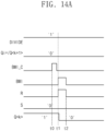
- FIGS. 14A and 14B are timing diagrams illustrating operations of the counting unit CU ⁇ k> performing both a complement operation and a division operation.
- FIG. 14A illustrates the complement operation and the division operation in the case where a count value Q ⁇ k> of the counting unit CU ⁇ k> is logic '1' and an inverted count value /Q ⁇ k+1> of the counting unit CU ⁇ k+1> is logic '0'.
- FIG. 14B illustrates the complement operation and the division operation in the case where the current count value Q ⁇ k> of the counting unit CU ⁇ k> is logic '0' and the inverted count value /Q ⁇ k+1> of the counting unit CU ⁇ k+1> is logic '1'.
- the second complement control signal BWI may transition to the high level.
- the output value Q ⁇ k> of the D-flip-flop 247 may transition to a reset value, that is, logic '0'.
- the inverted higher count value /Q ⁇ k+1> may be shifted to the lower count value Q ⁇ k> in the above manner.
- the complement operation and the division operation may be performed together.
- logic '1' corresponding to the inverted count value /Q ⁇ k+1> is stored in the D-latch 246a (refer to FIG. 11B ) of the complement operation controller 246 (refer to FIG. 11B ) in synchronization with a rising edge of the first complement control signal BWI_C.
- the second complement control signal BWI may transition to the high level.
- the output value Q ⁇ k> of the D-flip-flop 247 may transition to a set value, that is, logic '1'.
- the inverted higher count value /Q ⁇ k+1> may be shifted to the lower count value Q ⁇ k> in the above manner.
- the complement operation and the division operation may be performed together.
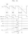
- FIG. 15 is a timing diagram illustrating a reset multiple sampling operation using a counter according to an example.
- the CDS output signal CDS_OUT transitions to the low level.
- the counting value of the counter CNT_j may maintain the level of "R1 + R2".
- the complement operation and the division operation are performed on the reset signal "R1 + R2".
- the sampled reset signal "R1 + R2" is converted into a negative number "-(R1 + R2)" through the complement operation.
- an average value of the reset signal corresponding to "-(R1 + R2)" may be obtained through the division operation.
- the counting value of the counter CNT_j may store the level of "-(R1 + R2)/2".
- the image signal "S” is sampled by using "-(R1 + R2)/2" as a start count value.
- the counter CNT_j performs a count-up operation from "-(R1 + R2)/2"
- a count value corresponding to "S - (R1+R2)/2” may be output from the counter CNT_j as a result of the count-up operation. That is, the average value "-(R1 + R2)/2" of the reset signal stored in a memory is applied to the counter CNT_j before the image signal "S" is sampled. As such, a count value corresponding to "S - (R1+R2)/2” may be set at the counter CNT_j.
- the counter according to an example may easily perform a multiple sampling operation by performing the complement operation and the division operation at the same time.
- it may be possible to implement a low-noise image sensor through the division operation of a multiple-sampled reset signal.
- FIGS. 16A and 16B are diagrams illustrating a structure of a pixel sensor of an image sensor for performing multiple sampling by using a counter according to an example.
- a pixel sensor 211 may be configured to include at least two photoelectric conversion elements.
- the pixel sensor 211 may be divided into a first sub-pixel C1 and a second sub-pixel C2.
- the first sub-pixel C1 may include a first photoelectric conversion element PD1 and a first transfer transistor TX1.
- the second sub-pixel C2 may include a second photoelectric conversion element PD2 and a second transfer transistor TX2.
- the first and second transfer transistors TX1 and TX2 may share the floating diffusion area FD1.
- a gate electrode of the first transfer transistor TX1 may be connected to a first charge transfer line TG1, and may transfer charges accumulated at the first photoelectric conversion element PD1 to the floating diffusion area FD1 in response to a first charge transfer signal.
- a gate electrode of the second transfer transistor TX2 may be connected to a second charge transfer line TG2, and may transfer charges accumulated at the second photoelectric conversion element PD2 to the floating diffusion area FD1 in response to a second charge transfer signal.
- the image signals SIG are sequentially generated by the first sub-pixel C1 and the second sub-pixel C2. Accordingly, an average value of the image signals obtained through the multiple sampling operation may be easily calculated through the complement operation and the division operation that are performed at the counter according to an example.
- FIG. 17 is a timing diagram illustrating an analog-to-digital converting operation of a reset multiple sampling scheme using a counter according to an example, in the pixel structure illustrated in FIG. 16B .
- the multiple sampling method may be applied to pixel structures illustrated in FIGS. 16A and 16B or to other pixel structures.
- the CDS output signal CDS_OUT transitions to the low level.
- the count value of the counter CNT_j may maintain the level of "R1 + R2".
- the second complement control signal BWI transitions to the high level after the division control signal DIVIDE and the first complement control signal BWI_C transition to the high level.
- the complement operation and the division operation are performed on the reset signal "R1 + R2" maintained at the counter CNT_j.
- the sampled reset signal "R1 + R2” is converted into a negative number "-(R1 + R2)” through the complement operation.
- an average value of the reset signal corresponding to "-(R1 + R2)/2” may be obtained through the division operation.
- the average value "-(R1 + R2)/2" of the reset signal corresponding to a negative number may be stored in a register or memory that is separately provided.
- the average value "-(R1 + R2)/2" of the reset signal may be maintained at the counter CNT_j.
- the first image signal S1 is sampled by using "-(R1 + R2)/2" as a start count value.
- the first image signal S1 may be, for example, an image signal Sig1 sensed from the first sub-pixel C1 of FIG. 16A .
- the counter CNT_j performs a count-up operation from "-(R1 + R2)/2". In this case, a count value may increase up to "S1 -(R1+R2)/2" until a time T7.
- a count value corresponding to "S1 -(R1+R2)/2” may be output from the counter CNT_j as a result of the count-up operation.
- the second image signal S2 is sampled by using "-(R1 + R2)/2" as a start count value.
- the second image signal S2 may be, for example, a sum of the image signals Sig1 and Sig2 sensed from the first sub-pixel C1 and the second sub-pixel C2 of FIG. 16A .
- the counter CNT_j performs a count-up operation from "-(R1 + R2)/2” As such, a count value may increase up to "S2 -(R1+R2)/2" at a time T9. Accordingly, "S2 - (R1+R2)/2" may be output as a counted value.
- the counter according to an example may easily perform a multiple sampling operation by performing the complement operation and the division operation at the same time.
- FIG. 18 is a block diagram illustrating an electronic system including an image sensor according to an example.
- an electronic system 1000 may be implemented with a data processing device, which uses or supports a mobile industry processor interface (MIPI), such as a mobile phone, a portable digital assistant (PDA), a personal media player (PMP), or a smartphone.
- MIPI mobile industry processor interface
- the electronic system 1000 may include an application processor 1010, an image sensor 1040, and a display 1050.
- a camera serial interface (CSI) host 1012 implemented in the application processor 1010 may perform serial communication with a CSI device 1041 of the image sensor 1040 through a CSI.
- an optical deserializer DES may be implemented in the CSI host 1012
- an optical serializer SER may be implemented in the CSI device 1041.
- the application processor 1010 may include an image signal processor (ISP) that performs auto white balancing.
- ISP image signal processor
- a display serial interface (DSI) host 1011 implemented in the application processor 1010 may perform serial communication with a DSI device 1051 of the display 1050 through a DSI.
- DSI display serial interface
- an optical serializer SER may be implemented in the DSI host 1011
- an optical deserializer DES may be implemented in the DSI device 1051.
- the electronic system 1000 may further include a radio frequency (RF) chip 1060 capable of communicating with the application processor 1010.
- RF radio frequency
- a physical layer (PHY) 1013 of the application processor 1010 and a physical layer (PHY) 1061 of the RF chip 1060 may exchange data in compliance with an MIPI DigRF interface.
- the electronic system 1000 may further include a GPS 1020, storage 1070, a microphone 1080, a DRAM 1085, and a speaker 1090, and the electronic system 1000 may communicate with an external device by using WiMAX 1030, WLAN 1033, UWB 1035, etc.
- data may be sampled in a way to subtract a count value corresponding to a reset signal RESET from a count value corresponding to an image signal SIG output from a pixel, for implementing a low noise device.
- the counter may use a function of a complement operation for subtracting the count value of the reset signal RESET.
- a coupling influence between signal lines may be increased and the possibility of failure of a complement operation of the counter may increase. The risk of such a failure is reduced by the use of a D-latch to store signal values for use in the complement operation, reducing the sensitivity to fluctuations in complement control signals.
- a counter having a division function is useful for applying a reset multiple sampling technique for low-noise implementation.
- embodiments relate to a semiconductor device, and more particularly, relate to a counter capable of performing a complement operation and an image sensor including the same.
- Examples may provide a counter having a division function capable of reducing the influence of coupling in a complement operation and applying a reset multiple sampling technique, and an image sensor including the same.
- a counter may be implemented that reduces the influence of coupling in a complement operation performed at an image sensor.
- a counter including a division function used in a reset multiple sampling scheme and an image sensor including the counter may be implemented.
Landscapes
- Engineering & Computer Science (AREA)
- Multimedia (AREA)
- Signal Processing (AREA)
- Theoretical Computer Science (AREA)
- Transforming Light Signals Into Electric Signals (AREA)
Claims (5)
- Zählerschaltung (CNT_0), die eine hohe Periode oder eine niedrige Periode eines Eingabesignals (CDS_OUT0) unter Verwendung eines Taktsignals (CLK) zählt, wobei die Zählerschaltung (CNT_0) Folgendes umfasst:ein erstes UND-Gate (141), das dafür konfiguriert ist, eine UND-Operation an dem Eingabesignal (CDS_OUT0) und dem Taktsignal (CLK) durchzuführen; undeinen Asynchronzähler, der durch eine Ausgabe des ersten UND-Gates (141) ausgelöst wird, um eine Länge des Eingabesignals (CDS_OUT0) zu zählen, wobei der Asynchronzähler eine Vielzahl von Zähleinheiten (142 - 145; CU<0> - CU<n-1>) zum Vorwärtszählen oder Rückwärtszählen der Länge des Eingabesignals (CDS_OUT0) einschließt, wobei jede der Vielzahl von Zähleinheiten (142 - 145; CU<0> - CU<n-1>) Folgendes einschließt:ein D-Latch (146a), das dafür konfiguriert ist, als Reaktion auf ein erstes Komplementsteuersignal (BWI_C) ein umgekehrtes Zählbit zu speichern; undein D-Flip-Flop (147), das als Antwort auf ein zweites Komplementsteuersignal (BWI) durch das in dem D-Latch (146a) gespeicherte umgekehrte Zählbit eingestellt oder zurückgesetzt wird, dadurch gekennzeichnet, dass jede der Vielzahl von Zähleinheiten (142 - 145; CU<0> - CU<n-1>) ferner eine Komplementoperationssteuerung (146) umfasst, die Folgendes einschließt:ein zweites UND-Gate (146b), das dafür konfiguriert ist, ein nicht umgekehrtes Ausgabesignal (Q) des D-Latch (146a) an einen eingestellten Eingabeanschluss (SET) des D-Flip-Flops (147) synchron mit dem zweiten Komplementsteuersignal (BWI) zu übertragen; undein drittes UND-Gate (146c), das dafür konfiguriert ist, ein umgekehrtes Ausgabesignal (/Q) des D-Latch (146a) an einen zurückgesetzten Eingabeanschluss (RESET) des D-Flip-Flops (147) synchron mit dem zweiten Komplementsteuersignal (BWI) zu übertragen.
- Zählerschaltung (CNT_0) nach Anspruch 1, wobei der Asynchronzähler Folgendes einschließt:eine erste Zähleinheit (142; CU<0>), die dafür konfiguriert ist, einen niedrigstwertigen Zählwert (Q<0>) synchron mit einer fallenden Flanke einer Ausgabe des ersten UND-Gate (141) umzuschalten; undeine zweite Zähleinheit (143; CU< 1 >), die von einer fallenden Flanke einer Ausgabe (Q) der ersten Zähleinheit (142; CU<0>) ausgelöst wird.
- Zählerschaltung (CNT_0) nach Anspruch 2, wobei ein umgekehrter Ausgabeanschluss (/Q) der ersten Zähleinheit (142; CU<0>) mit einem Dateneingabeanschluss (D) der ersten Zähleinheit (142; CU<0>) verbunden ist.
- Zählerschaltung (CNT_0) nach einem der Ansprüche 1 bis 3, wobei das erste Komplementsteuersignal (BWI_C) und das zweite Komplementsteuersignal (BWI) dafür konfiguriert sind, sequentiell zu einem hohen Pegel überzugehen, um ein Komplement von aktuellen Zählbits des Asynchronzählers zu erzeugen.
- Bildsensor umfassend die Zählerschaltung nach einem vorhergehenden Anspruch.
Applications Claiming Priority (3)
| Application Number | Priority Date | Filing Date | Title |
|---|---|---|---|
| KR1020190129942A KR102946263B1 (ko) | 2019-10-18 | 2019-10-18 | 카운터 회로 및 그것을 포함하는 이미지 센서 |
| US16/908,980 US11451731B2 (en) | 2019-10-18 | 2020-06-23 | Counter circuit and image sensor including the same |
| EP20197914.3A EP3809695B1 (de) | 2019-10-18 | 2020-09-23 | Zählerschaltung und bildsensor damit |
Related Parent Applications (2)
| Application Number | Title | Priority Date | Filing Date |
|---|---|---|---|
| EP20197914.3A Division-Into EP3809695B1 (de) | 2019-10-18 | 2020-09-23 | Zählerschaltung und bildsensor damit |
| EP20197914.3A Division EP3809695B1 (de) | 2019-10-18 | 2020-09-23 | Zählerschaltung und bildsensor damit |
Publications (2)
| Publication Number | Publication Date |
|---|---|
| EP3962070A1 EP3962070A1 (de) | 2022-03-02 |
| EP3962070B1 true EP3962070B1 (de) | 2024-05-15 |
Family
ID=75491726
Family Applications (1)
| Application Number | Title | Priority Date | Filing Date |
|---|---|---|---|
| EP21202028.3A Active EP3962070B1 (de) | 2019-10-18 | 2020-09-23 | Zählerschaltung und hiermit versehener bildsensor |
Country Status (4)
| Country | Link |
|---|---|
| US (1) | US11451731B2 (de) |
| EP (1) | EP3962070B1 (de) |
| JP (1) | JP7582596B2 (de) |
| KR (1) | KR102946263B1 (de) |
Families Citing this family (2)
| Publication number | Priority date | Publication date | Assignee | Title |
|---|---|---|---|---|
| WO2024259802A1 (zh) * | 2023-06-19 | 2024-12-26 | 思特威(上海)电子科技股份有限公司 | 图像传感器及其读出电路 |
| TW202510513A (zh) * | 2023-08-28 | 2025-03-01 | 南韓商三星電子股份有限公司 | 雙向計數器和產生輸出資料的方法 |
Family Cites Families (14)
| Publication number | Priority date | Publication date | Assignee | Title |
|---|---|---|---|---|
| US3872466A (en) * | 1973-07-19 | 1975-03-18 | Analog Devices Inc | Integrating analog-to-digital converter having digitally-derived offset error compensation and bipolar operation without zero discontinuity |
| JP4853445B2 (ja) * | 2007-09-28 | 2012-01-11 | ソニー株式会社 | A/d変換回路、固体撮像素子、およびカメラシステム |
| KR101621244B1 (ko) * | 2009-02-13 | 2016-05-16 | 삼성전자주식회사 | 카운터 회로, 이를 포함하는 장치 및 카운팅 방법 |
| KR101365408B1 (ko) | 2009-03-03 | 2014-02-19 | 삼성전자주식회사 | 카운터 회로, 이를 포함하는 물리량 측정 장치 및 카운팅 방법 |
| JP5254140B2 (ja) * | 2009-07-14 | 2013-08-07 | 株式会社東芝 | A/d変換器及びそれを備えた固体撮像装置 |
| KR101647366B1 (ko) * | 2009-09-25 | 2016-08-11 | 삼성전자주식회사 | 카운터 회로, 이를 포함하는 장치 및 카운팅 방법 |
| US8586903B2 (en) | 2009-11-23 | 2013-11-19 | Samsung Electronics Co., Ltd. | Counter circuits, analog to digital converters, image sensors and digital imaging systems including the same |
| US8969770B2 (en) | 2011-05-02 | 2015-03-03 | Semiconductor Components Industries, Llc | Correlated double sampling to include a controller to increment and invert a count during a first period and a second period |
| US8576979B2 (en) | 2011-10-11 | 2013-11-05 | Omnivision Technologies, Inc. | Arithmetic counter circuit, configuration and application for high performance CMOS image sensors |
| JP6019793B2 (ja) | 2012-06-20 | 2016-11-02 | ソニー株式会社 | カウンタ、カウント方法、ad変換装置、固体撮像素子、および電子装置 |
| KR102135684B1 (ko) | 2013-07-24 | 2020-07-20 | 삼성전자주식회사 | 카운터 회로, 이를 포함하는 아날로그-디지털 컨버터, 이미지 센서 및 이를 이용하는 상관 이중 샘플링 방법 |
| KR102082288B1 (ko) | 2013-12-12 | 2020-02-27 | 에스케이하이닉스 주식회사 | 이중 데이터 레이트 카운터 및 그를 이용한 아날로그-디지털 변환 장치와 씨모스 이미지 센서 |
| US9960783B2 (en) | 2015-09-18 | 2018-05-01 | Taiwan Semiconductor Manufacturing Company Ltd. | Conditional correlated multiple sampling single slope analog-to-digital converter, and associated image sensor system and method |
| US9774333B2 (en) | 2015-10-14 | 2017-09-26 | Stmicroelectronics (Grenoble 2) Sas | Counter circuit |
-
2019
- 2019-10-18 KR KR1020190129942A patent/KR102946263B1/ko active Active
-
2020
- 2020-06-23 US US16/908,980 patent/US11451731B2/en active Active
- 2020-09-23 EP EP21202028.3A patent/EP3962070B1/de active Active
- 2020-10-07 JP JP2020169542A patent/JP7582596B2/ja active Active
Also Published As
| Publication number | Publication date |
|---|---|
| US20210120201A1 (en) | 2021-04-22 |
| JP2021069112A (ja) | 2021-04-30 |
| EP3962070A1 (de) | 2022-03-02 |
| JP7582596B2 (ja) | 2024-11-13 |
| KR102946263B1 (ko) | 2026-04-01 |
| KR20210046897A (ko) | 2021-04-29 |
| US11451731B2 (en) | 2022-09-20 |
Similar Documents
| Publication | Publication Date | Title |
|---|---|---|
| US11758305B2 (en) | Comparator, ad converter, solid-state imaging device, electronic apparatus, and method of controlling comparator | |
| US11641534B2 (en) | Gray counter and image sensor including the same | |
| US10257452B2 (en) | Solid-state image pickup apparatus, signal processing method for a solid-state image pickup apparatus, and electronic apparatus | |
| US9819885B2 (en) | Solid-state imaging device and imaging system | |
| US9185316B2 (en) | Data sampler, data sampling method, and photo detecting apparatus including data sampler that minimizes the effect of offset | |
| US9232161B2 (en) | Unit pixels configured to output different pixel signals through different lines and image sensors including the same | |
| US20100207798A1 (en) | Double data rate (DDR) counter, analog-to-digital converter (ADC) using the same, CMOS image sensor using the same and methods in DDR counter, ADC and CMOS image sensor | |
| US11284026B2 (en) | Image sensor | |
| US11451731B2 (en) | Counter circuit and image sensor including the same | |
| US12581221B2 (en) | Comparator and image sensor including the same | |
| EP3809695B1 (de) | Zählerschaltung und bildsensor damit | |
| KR102136851B1 (ko) | 컬럼 미스매치를 보상하는 이미지 센서 및 이의 이미지 처리 방법 | |
| JP2020188360A (ja) | 固体撮像素子およびその駆動方法 |
Legal Events
| Date | Code | Title | Description |
|---|---|---|---|
| PUAI | Public reference made under article 153(3) epc to a published international application that has entered the european phase |
Free format text: ORIGINAL CODE: 0009012 |
|
| STAA | Information on the status of an ep patent application or granted ep patent |
Free format text: STATUS: REQUEST FOR EXAMINATION WAS MADE |
|
| 17P | Request for examination filed |
Effective date: 20211011 |
|
| AC | Divisional application: reference to earlier application |
Ref document number: 3809695 Country of ref document: EP Kind code of ref document: P |
|
| AK | Designated contracting states |
Kind code of ref document: A1 Designated state(s): AL AT BE BG CH CY CZ DE DK EE ES FI FR GB GR HR HU IE IS IT LI LT LU LV MC MK MT NL NO PL PT RO RS SE SI SK SM TR |
|
| P01 | Opt-out of the competence of the unified patent court (upc) registered |
Effective date: 20230519 |
|
| REG | Reference to a national code |
Ipc: H04N0025460000 Ref country code: DE Ref legal event code: R079 Ref document number: 602020031139 Country of ref document: DE Free format text: PREVIOUS MAIN CLASS: H04N0005378000 |
|
| GRAP | Despatch of communication of intention to grant a patent |
Free format text: ORIGINAL CODE: EPIDOSNIGR1 |
|
| STAA | Information on the status of an ep patent application or granted ep patent |
Free format text: STATUS: GRANT OF PATENT IS INTENDED |
|
| RIC1 | Information provided on ipc code assigned before grant |
Ipc: H03M 1/56 20060101ALI20240111BHEP Ipc: H03M 1/12 20060101ALI20240111BHEP Ipc: H04N 25/75 20230101ALI20240111BHEP Ipc: H04N 25/616 20230101ALI20240111BHEP Ipc: H04N 25/46 20230101AFI20240111BHEP |
|
| INTG | Intention to grant announced |
Effective date: 20240206 |
|
| GRAS | Grant fee paid |
Free format text: ORIGINAL CODE: EPIDOSNIGR3 |
|
| GRAA | (expected) grant |
Free format text: ORIGINAL CODE: 0009210 |
|
| STAA | Information on the status of an ep patent application or granted ep patent |
Free format text: STATUS: THE PATENT HAS BEEN GRANTED |
|
| AC | Divisional application: reference to earlier application |
Ref document number: 3809695 Country of ref document: EP Kind code of ref document: P |
|
| AK | Designated contracting states |
Kind code of ref document: B1 Designated state(s): AL AT BE BG CH CY CZ DE DK EE ES FI FR GB GR HR HU IE IS IT LI LT LU LV MC MK MT NL NO PL PT RO RS SE SI SK SM TR |
|
| REG | Reference to a national code |
Ref country code: CH Ref legal event code: EP |
|
| REG | Reference to a national code |
Ref country code: IE Ref legal event code: FG4D |
|
| REG | Reference to a national code |
Ref country code: DE Ref legal event code: R096 Ref document number: 602020031139 Country of ref document: DE |
|
| REG | Reference to a national code |
Ref country code: NL Ref legal event code: FP |
|
| REG | Reference to a national code |
Ref country code: LT Ref legal event code: MG9D |
|
| PG25 | Lapsed in a contracting state [announced via postgrant information from national office to epo] |
Ref country code: IS Free format text: LAPSE BECAUSE OF FAILURE TO SUBMIT A TRANSLATION OF THE DESCRIPTION OR TO PAY THE FEE WITHIN THE PRESCRIBED TIME-LIMIT Effective date: 20240915 |
|
| PG25 | Lapsed in a contracting state [announced via postgrant information from national office to epo] |
Ref country code: BG Free format text: LAPSE BECAUSE OF FAILURE TO SUBMIT A TRANSLATION OF THE DESCRIPTION OR TO PAY THE FEE WITHIN THE PRESCRIBED TIME-LIMIT Effective date: 20240515 |
|
| PG25 | Lapsed in a contracting state [announced via postgrant information from national office to epo] |
Ref country code: HR Free format text: LAPSE BECAUSE OF FAILURE TO SUBMIT A TRANSLATION OF THE DESCRIPTION OR TO PAY THE FEE WITHIN THE PRESCRIBED TIME-LIMIT Effective date: 20240515 Ref country code: FI Free format text: LAPSE BECAUSE OF FAILURE TO SUBMIT A TRANSLATION OF THE DESCRIPTION OR TO PAY THE FEE WITHIN THE PRESCRIBED TIME-LIMIT Effective date: 20240515 |
|
| PG25 | Lapsed in a contracting state [announced via postgrant information from national office to epo] |
Ref country code: GR Free format text: LAPSE BECAUSE OF FAILURE TO SUBMIT A TRANSLATION OF THE DESCRIPTION OR TO PAY THE FEE WITHIN THE PRESCRIBED TIME-LIMIT Effective date: 20240816 |
|
| PG25 | Lapsed in a contracting state [announced via postgrant information from national office to epo] |
Ref country code: PT Free format text: LAPSE BECAUSE OF FAILURE TO SUBMIT A TRANSLATION OF THE DESCRIPTION OR TO PAY THE FEE WITHIN THE PRESCRIBED TIME-LIMIT Effective date: 20240916 |
|
| REG | Reference to a national code |
Ref country code: AT Ref legal event code: MK05 Ref document number: 1687857 Country of ref document: AT Kind code of ref document: T Effective date: 20240515 |
|
| PG25 | Lapsed in a contracting state [announced via postgrant information from national office to epo] |
Ref country code: ES Free format text: LAPSE BECAUSE OF FAILURE TO SUBMIT A TRANSLATION OF THE DESCRIPTION OR TO PAY THE FEE WITHIN THE PRESCRIBED TIME-LIMIT Effective date: 20240515 |
|
| PG25 | Lapsed in a contracting state [announced via postgrant information from national office to epo] |
Ref country code: AT Free format text: LAPSE BECAUSE OF FAILURE TO SUBMIT A TRANSLATION OF THE DESCRIPTION OR TO PAY THE FEE WITHIN THE PRESCRIBED TIME-LIMIT Effective date: 20240515 |
|
| PG25 | Lapsed in a contracting state [announced via postgrant information from national office to epo] |
Ref country code: PL Free format text: LAPSE BECAUSE OF FAILURE TO SUBMIT A TRANSLATION OF THE DESCRIPTION OR TO PAY THE FEE WITHIN THE PRESCRIBED TIME-LIMIT Effective date: 20240515 |
|
| PG25 | Lapsed in a contracting state [announced via postgrant information from national office to epo] |
Ref country code: LV Free format text: LAPSE BECAUSE OF FAILURE TO SUBMIT A TRANSLATION OF THE DESCRIPTION OR TO PAY THE FEE WITHIN THE PRESCRIBED TIME-LIMIT Effective date: 20240515 |
|
| PG25 | Lapsed in a contracting state [announced via postgrant information from national office to epo] |
Ref country code: PT Free format text: LAPSE BECAUSE OF FAILURE TO SUBMIT A TRANSLATION OF THE DESCRIPTION OR TO PAY THE FEE WITHIN THE PRESCRIBED TIME-LIMIT Effective date: 20240916 Ref country code: PL Free format text: LAPSE BECAUSE OF FAILURE TO SUBMIT A TRANSLATION OF THE DESCRIPTION OR TO PAY THE FEE WITHIN THE PRESCRIBED TIME-LIMIT Effective date: 20240515 Ref country code: NO Free format text: LAPSE BECAUSE OF FAILURE TO SUBMIT A TRANSLATION OF THE DESCRIPTION OR TO PAY THE FEE WITHIN THE PRESCRIBED TIME-LIMIT Effective date: 20240815 Ref country code: LV Free format text: LAPSE BECAUSE OF FAILURE TO SUBMIT A TRANSLATION OF THE DESCRIPTION OR TO PAY THE FEE WITHIN THE PRESCRIBED TIME-LIMIT Effective date: 20240515 Ref country code: IS Free format text: LAPSE BECAUSE OF FAILURE TO SUBMIT A TRANSLATION OF THE DESCRIPTION OR TO PAY THE FEE WITHIN THE PRESCRIBED TIME-LIMIT Effective date: 20240915 Ref country code: HR Free format text: LAPSE BECAUSE OF FAILURE TO SUBMIT A TRANSLATION OF THE DESCRIPTION OR TO PAY THE FEE WITHIN THE PRESCRIBED TIME-LIMIT Effective date: 20240515 Ref country code: GR Free format text: LAPSE BECAUSE OF FAILURE TO SUBMIT A TRANSLATION OF THE DESCRIPTION OR TO PAY THE FEE WITHIN THE PRESCRIBED TIME-LIMIT Effective date: 20240816 Ref country code: FI Free format text: LAPSE BECAUSE OF FAILURE TO SUBMIT A TRANSLATION OF THE DESCRIPTION OR TO PAY THE FEE WITHIN THE PRESCRIBED TIME-LIMIT Effective date: 20240515 Ref country code: ES Free format text: LAPSE BECAUSE OF FAILURE TO SUBMIT A TRANSLATION OF THE DESCRIPTION OR TO PAY THE FEE WITHIN THE PRESCRIBED TIME-LIMIT Effective date: 20240515 Ref country code: BG Free format text: LAPSE BECAUSE OF FAILURE TO SUBMIT A TRANSLATION OF THE DESCRIPTION OR TO PAY THE FEE WITHIN THE PRESCRIBED TIME-LIMIT Effective date: 20240515 Ref country code: AT Free format text: LAPSE BECAUSE OF FAILURE TO SUBMIT A TRANSLATION OF THE DESCRIPTION OR TO PAY THE FEE WITHIN THE PRESCRIBED TIME-LIMIT Effective date: 20240515 Ref country code: RS Free format text: LAPSE BECAUSE OF FAILURE TO SUBMIT A TRANSLATION OF THE DESCRIPTION OR TO PAY THE FEE WITHIN THE PRESCRIBED TIME-LIMIT Effective date: 20240815 |
|
| PG25 | Lapsed in a contracting state [announced via postgrant information from national office to epo] |
Ref country code: DK Free format text: LAPSE BECAUSE OF FAILURE TO SUBMIT A TRANSLATION OF THE DESCRIPTION OR TO PAY THE FEE WITHIN THE PRESCRIBED TIME-LIMIT Effective date: 20240515 |
|
| PG25 | Lapsed in a contracting state [announced via postgrant information from national office to epo] |
Ref country code: EE Free format text: LAPSE BECAUSE OF FAILURE TO SUBMIT A TRANSLATION OF THE DESCRIPTION OR TO PAY THE FEE WITHIN THE PRESCRIBED TIME-LIMIT Effective date: 20240515 |
|
| PG25 | Lapsed in a contracting state [announced via postgrant information from national office to epo] |
Ref country code: CZ Free format text: LAPSE BECAUSE OF FAILURE TO SUBMIT A TRANSLATION OF THE DESCRIPTION OR TO PAY THE FEE WITHIN THE PRESCRIBED TIME-LIMIT Effective date: 20240515 |
|
| PG25 | Lapsed in a contracting state [announced via postgrant information from national office to epo] |
Ref country code: SK Free format text: LAPSE BECAUSE OF FAILURE TO SUBMIT A TRANSLATION OF THE DESCRIPTION OR TO PAY THE FEE WITHIN THE PRESCRIBED TIME-LIMIT Effective date: 20240515 Ref country code: RO Free format text: LAPSE BECAUSE OF FAILURE TO SUBMIT A TRANSLATION OF THE DESCRIPTION OR TO PAY THE FEE WITHIN THE PRESCRIBED TIME-LIMIT Effective date: 20240515 |
|
| PG25 | Lapsed in a contracting state [announced via postgrant information from national office to epo] |
Ref country code: SM Free format text: LAPSE BECAUSE OF FAILURE TO SUBMIT A TRANSLATION OF THE DESCRIPTION OR TO PAY THE FEE WITHIN THE PRESCRIBED TIME-LIMIT Effective date: 20240515 |
|
| PG25 | Lapsed in a contracting state [announced via postgrant information from national office to epo] |
Ref country code: SM Free format text: LAPSE BECAUSE OF FAILURE TO SUBMIT A TRANSLATION OF THE DESCRIPTION OR TO PAY THE FEE WITHIN THE PRESCRIBED TIME-LIMIT Effective date: 20240515 Ref country code: SK Free format text: LAPSE BECAUSE OF FAILURE TO SUBMIT A TRANSLATION OF THE DESCRIPTION OR TO PAY THE FEE WITHIN THE PRESCRIBED TIME-LIMIT Effective date: 20240515 Ref country code: RO Free format text: LAPSE BECAUSE OF FAILURE TO SUBMIT A TRANSLATION OF THE DESCRIPTION OR TO PAY THE FEE WITHIN THE PRESCRIBED TIME-LIMIT Effective date: 20240515 Ref country code: EE Free format text: LAPSE BECAUSE OF FAILURE TO SUBMIT A TRANSLATION OF THE DESCRIPTION OR TO PAY THE FEE WITHIN THE PRESCRIBED TIME-LIMIT Effective date: 20240515 Ref country code: DK Free format text: LAPSE BECAUSE OF FAILURE TO SUBMIT A TRANSLATION OF THE DESCRIPTION OR TO PAY THE FEE WITHIN THE PRESCRIBED TIME-LIMIT Effective date: 20240515 Ref country code: CZ Free format text: LAPSE BECAUSE OF FAILURE TO SUBMIT A TRANSLATION OF THE DESCRIPTION OR TO PAY THE FEE WITHIN THE PRESCRIBED TIME-LIMIT Effective date: 20240515 |
|
| PG25 | Lapsed in a contracting state [announced via postgrant information from national office to epo] |
Ref country code: IT Free format text: LAPSE BECAUSE OF FAILURE TO SUBMIT A TRANSLATION OF THE DESCRIPTION OR TO PAY THE FEE WITHIN THE PRESCRIBED TIME-LIMIT Effective date: 20240515 |
|
| REG | Reference to a national code |
Ref country code: DE Ref legal event code: R097 Ref document number: 602020031139 Country of ref document: DE |
|
| PLBE | No opposition filed within time limit |
Free format text: ORIGINAL CODE: 0009261 |
|
| STAA | Information on the status of an ep patent application or granted ep patent |
Free format text: STATUS: NO OPPOSITION FILED WITHIN TIME LIMIT |
|
| 26N | No opposition filed |
Effective date: 20250218 |
|
| PG25 | Lapsed in a contracting state [announced via postgrant information from national office to epo] |
Ref country code: MC Free format text: LAPSE BECAUSE OF FAILURE TO SUBMIT A TRANSLATION OF THE DESCRIPTION OR TO PAY THE FEE WITHIN THE PRESCRIBED TIME-LIMIT Effective date: 20240515 Ref country code: SI Free format text: LAPSE BECAUSE OF FAILURE TO SUBMIT A TRANSLATION OF THE DESCRIPTION OR TO PAY THE FEE WITHIN THE PRESCRIBED TIME-LIMIT Effective date: 20240515 |
|
| REG | Reference to a national code |
Ref country code: CH Ref legal event code: PL |
|
| PG25 | Lapsed in a contracting state [announced via postgrant information from national office to epo] |
Ref country code: LU Free format text: LAPSE BECAUSE OF NON-PAYMENT OF DUE FEES Effective date: 20240923 |
|
| REG | Reference to a national code |
Ref country code: BE Ref legal event code: MM Effective date: 20240930 |
|
| PG25 | Lapsed in a contracting state [announced via postgrant information from national office to epo] |
Ref country code: BE Free format text: LAPSE BECAUSE OF NON-PAYMENT OF DUE FEES Effective date: 20240930 |
|
| PG25 | Lapsed in a contracting state [announced via postgrant information from national office to epo] |
Ref country code: FR Free format text: LAPSE BECAUSE OF NON-PAYMENT OF DUE FEES Effective date: 20240930 |
|
| PG25 | Lapsed in a contracting state [announced via postgrant information from national office to epo] |
Ref country code: CH Free format text: LAPSE BECAUSE OF NON-PAYMENT OF DUE FEES Effective date: 20240930 |
|
| PG25 | Lapsed in a contracting state [announced via postgrant information from national office to epo] |
Ref country code: IE Free format text: LAPSE BECAUSE OF NON-PAYMENT OF DUE FEES Effective date: 20240923 |
|
| PG25 | Lapsed in a contracting state [announced via postgrant information from national office to epo] |
Ref country code: SE Free format text: LAPSE BECAUSE OF FAILURE TO SUBMIT A TRANSLATION OF THE DESCRIPTION OR TO PAY THE FEE WITHIN THE PRESCRIBED TIME-LIMIT Effective date: 20240515 |
|
| PGFP | Annual fee paid to national office [announced via postgrant information from national office to epo] |
Ref country code: NL Payment date: 20250814 Year of fee payment: 6 |
|
| PGFP | Annual fee paid to national office [announced via postgrant information from national office to epo] |
Ref country code: DE Payment date: 20250730 Year of fee payment: 6 |
|
| PGFP | Annual fee paid to national office [announced via postgrant information from national office to epo] |
Ref country code: GB Payment date: 20250731 Year of fee payment: 6 |
|
| PG25 | Lapsed in a contracting state [announced via postgrant information from national office to epo] |
Ref country code: CY Free format text: LAPSE BECAUSE OF FAILURE TO SUBMIT A TRANSLATION OF THE DESCRIPTION OR TO PAY THE FEE WITHIN THE PRESCRIBED TIME-LIMIT; INVALID AB INITIO Effective date: 20200923 |
|
| PG25 | Lapsed in a contracting state [announced via postgrant information from national office to epo] |
Ref country code: HU Free format text: LAPSE BECAUSE OF FAILURE TO SUBMIT A TRANSLATION OF THE DESCRIPTION OR TO PAY THE FEE WITHIN THE PRESCRIBED TIME-LIMIT; INVALID AB INITIO Effective date: 20200923 |
|
| PG25 | Lapsed in a contracting state [announced via postgrant information from national office to epo] |
Ref country code: TR Free format text: LAPSE BECAUSE OF FAILURE TO SUBMIT A TRANSLATION OF THE DESCRIPTION OR TO PAY THE FEE WITHIN THE PRESCRIBED TIME-LIMIT Effective date: 20240515 |
|
| PG25 | Lapsed in a contracting state [announced via postgrant information from national office to epo] |
Ref country code: LT Free format text: LAPSE BECAUSE OF FAILURE TO SUBMIT A TRANSLATION OF THE DESCRIPTION OR TO PAY THE FEE WITHIN THE PRESCRIBED TIME-LIMIT Effective date: 20240515 |