EP3961276B1 - Loss monitoring in photonic circuit fabrication - Google Patents
Loss monitoring in photonic circuit fabrication Download PDFInfo
- Publication number
- EP3961276B1 EP3961276B1 EP20208734.2A EP20208734A EP3961276B1 EP 3961276 B1 EP3961276 B1 EP 3961276B1 EP 20208734 A EP20208734 A EP 20208734A EP 3961276 B1 EP3961276 B1 EP 3961276B1
- Authority
- EP
- European Patent Office
- Prior art keywords
- fabrication
- integrated circuit
- photonic integrated
- optical
- damage
- Prior art date
- Legal status (The legal status is an assumption and is not a legal conclusion. Google has not performed a legal analysis and makes no representation as to the accuracy of the status listed.)
- Active
Links
Images



Classifications
-
- G—PHYSICS
- G01—MEASURING; TESTING
- G01N—INVESTIGATING OR ANALYSING MATERIALS BY DETERMINING THEIR CHEMICAL OR PHYSICAL PROPERTIES
- G01N21/00—Investigating or analysing materials by the use of optical means, i.e. using sub-millimetre waves, infrared, visible or ultraviolet light
- G01N21/84—Systems specially adapted for particular applications
- G01N21/88—Investigating the presence of flaws or contamination
- G01N21/95—Investigating the presence of flaws or contamination characterised by the material or shape of the object to be examined
- G01N21/9501—Semiconductor wafers
- G01N21/9505—Wafer internal defects, e.g. microcracks
-
- G—PHYSICS
- G01—MEASURING; TESTING
- G01M—TESTING STATIC OR DYNAMIC BALANCE OF MACHINES OR STRUCTURES; TESTING OF STRUCTURES OR APPARATUS, NOT OTHERWISE PROVIDED FOR
- G01M11/00—Testing of optical apparatus; Testing structures by optical methods not otherwise provided for
- G01M11/30—Testing of optical devices, constituted by fibre optics or optical waveguides
- G01M11/33—Testing of optical devices, constituted by fibre optics or optical waveguides with a light emitter being disposed at one fibre or waveguide end-face, and a light receiver at the other end-face
- G01M11/331—Testing of optical devices, constituted by fibre optics or optical waveguides with a light emitter being disposed at one fibre or waveguide end-face, and a light receiver at the other end-face by using interferometer
-
- G—PHYSICS
- G01—MEASURING; TESTING
- G01N—INVESTIGATING OR ANALYSING MATERIALS BY DETERMINING THEIR CHEMICAL OR PHYSICAL PROPERTIES
- G01N21/00—Investigating or analysing materials by the use of optical means, i.e. using sub-millimetre waves, infrared, visible or ultraviolet light
- G01N21/17—Systems in which incident light is modified in accordance with the properties of the material investigated
- G01N21/41—Refractivity; Phase-affecting properties, e.g. optical path length
- G01N21/45—Refractivity; Phase-affecting properties, e.g. optical path length using interferometric methods; using Schlieren methods
-
- G—PHYSICS
- G02—OPTICS
- G02B—OPTICAL ELEMENTS, SYSTEMS OR APPARATUS
- G02B6/00—Light guides; Structural details of arrangements comprising light guides and other optical elements, e.g. couplings
- G02B6/10—Light guides; Structural details of arrangements comprising light guides and other optical elements, e.g. couplings of the optical waveguide type
- G02B6/12—Light guides; Structural details of arrangements comprising light guides and other optical elements, e.g. couplings of the optical waveguide type of the integrated circuit kind
- G02B6/12002—Three-dimensional structures
-
- G—PHYSICS
- G02—OPTICS
- G02B—OPTICAL ELEMENTS, SYSTEMS OR APPARATUS
- G02B6/00—Light guides; Structural details of arrangements comprising light guides and other optical elements, e.g. couplings
- G02B6/10—Light guides; Structural details of arrangements comprising light guides and other optical elements, e.g. couplings of the optical waveguide type
- G02B6/12—Light guides; Structural details of arrangements comprising light guides and other optical elements, e.g. couplings of the optical waveguide type of the integrated circuit kind
- G02B6/12004—Combinations of two or more optical elements
-
- G—PHYSICS
- G02—OPTICS
- G02B—OPTICAL ELEMENTS, SYSTEMS OR APPARATUS
- G02B6/00—Light guides; Structural details of arrangements comprising light guides and other optical elements, e.g. couplings
- G02B6/10—Light guides; Structural details of arrangements comprising light guides and other optical elements, e.g. couplings of the optical waveguide type
- G02B6/12—Light guides; Structural details of arrangements comprising light guides and other optical elements, e.g. couplings of the optical waveguide type of the integrated circuit kind
- G02B6/13—Integrated optical circuits characterised by the manufacturing method
-
- G—PHYSICS
- G02—OPTICS
- G02F—OPTICAL DEVICES OR ARRANGEMENTS FOR THE CONTROL OF LIGHT BY MODIFICATION OF THE OPTICAL PROPERTIES OF THE MEDIA OF THE ELEMENTS INVOLVED THEREIN; NON-LINEAR OPTICS; FREQUENCY-CHANGING OF LIGHT; OPTICAL LOGIC ELEMENTS; OPTICAL ANALOGUE/DIGITAL CONVERTERS
- G02F1/00—Devices or arrangements for the control of the intensity, colour, phase, polarisation or direction of light arriving from an independent light source, e.g. switching, gating or modulating; Non-linear optics
- G02F1/01—Devices or arrangements for the control of the intensity, colour, phase, polarisation or direction of light arriving from an independent light source, e.g. switching, gating or modulating; Non-linear optics for the control of the intensity, phase, polarisation or colour
- G02F1/21—Devices or arrangements for the control of the intensity, colour, phase, polarisation or direction of light arriving from an independent light source, e.g. switching, gating or modulating; Non-linear optics for the control of the intensity, phase, polarisation or colour by interference
- G02F1/225—Devices or arrangements for the control of the intensity, colour, phase, polarisation or direction of light arriving from an independent light source, e.g. switching, gating or modulating; Non-linear optics for the control of the intensity, phase, polarisation or colour by interference in an optical waveguide structure
-
- G—PHYSICS
- G01—MEASURING; TESTING
- G01N—INVESTIGATING OR ANALYSING MATERIALS BY DETERMINING THEIR CHEMICAL OR PHYSICAL PROPERTIES
- G01N2201/00—Features of devices classified in G01N21/00
- G01N2201/06—Illumination; Optics
- G01N2201/061—Sources
- G01N2201/06113—Coherent sources; lasers
-
- G—PHYSICS
- G01—MEASURING; TESTING
- G01N—INVESTIGATING OR ANALYSING MATERIALS BY DETERMINING THEIR CHEMICAL OR PHYSICAL PROPERTIES
- G01N2201/00—Features of devices classified in G01N21/00
- G01N2201/08—Optical fibres; light guides
-
- G—PHYSICS
- G02—OPTICS
- G02B—OPTICAL ELEMENTS, SYSTEMS OR APPARATUS
- G02B6/00—Light guides; Structural details of arrangements comprising light guides and other optical elements, e.g. couplings
- G02B6/10—Light guides; Structural details of arrangements comprising light guides and other optical elements, e.g. couplings of the optical waveguide type
- G02B6/12—Light guides; Structural details of arrangements comprising light guides and other optical elements, e.g. couplings of the optical waveguide type of the integrated circuit kind
- G02B2006/12133—Functions
- G02B2006/12142—Modulator
-
- G—PHYSICS
- G02—OPTICS
- G02B—OPTICAL ELEMENTS, SYSTEMS OR APPARATUS
- G02B6/00—Light guides; Structural details of arrangements comprising light guides and other optical elements, e.g. couplings
- G02B6/10—Light guides; Structural details of arrangements comprising light guides and other optical elements, e.g. couplings of the optical waveguide type
- G02B6/12—Light guides; Structural details of arrangements comprising light guides and other optical elements, e.g. couplings of the optical waveguide type of the integrated circuit kind
- G02B2006/12133—Functions
- G02B2006/12159—Interferometer
-
- G—PHYSICS
- G02—OPTICS
- G02B—OPTICAL ELEMENTS, SYSTEMS OR APPARATUS
- G02B6/00—Light guides; Structural details of arrangements comprising light guides and other optical elements, e.g. couplings
- G02B6/10—Light guides; Structural details of arrangements comprising light guides and other optical elements, e.g. couplings of the optical waveguide type
- G02B6/12—Light guides; Structural details of arrangements comprising light guides and other optical elements, e.g. couplings of the optical waveguide type of the integrated circuit kind
- G02B2006/12166—Manufacturing methods
-
- G—PHYSICS
- G02—OPTICS
- G02F—OPTICAL DEVICES OR ARRANGEMENTS FOR THE CONTROL OF LIGHT BY MODIFICATION OF THE OPTICAL PROPERTIES OF THE MEDIA OF THE ELEMENTS INVOLVED THEREIN; NON-LINEAR OPTICS; FREQUENCY-CHANGING OF LIGHT; OPTICAL LOGIC ELEMENTS; OPTICAL ANALOGUE/DIGITAL CONVERTERS
- G02F1/00—Devices or arrangements for the control of the intensity, colour, phase, polarisation or direction of light arriving from an independent light source, e.g. switching, gating or modulating; Non-linear optics
- G02F1/01—Devices or arrangements for the control of the intensity, colour, phase, polarisation or direction of light arriving from an independent light source, e.g. switching, gating or modulating; Non-linear optics for the control of the intensity, phase, polarisation or colour
- G02F1/21—Devices or arrangements for the control of the intensity, colour, phase, polarisation or direction of light arriving from an independent light source, e.g. switching, gating or modulating; Non-linear optics for the control of the intensity, phase, polarisation or colour by interference
- G02F1/212—Mach-Zehnder type
Definitions
- the present disclosure generally relates to optical circuits, and more particularly to optical testing of circuits.
- the foundry can use in-line electrical measurements and electrical monitor structures to characterize the manufacturing process to ensure the material being delivered is of good quality.
- a single wafer can be fabricated that includes multiple photonic integrated circuits, which are then singulated into individual dies that undergo final testing. Generally, a portion of the dies have errors that result from the fabrication process and are scrapped after the final tests. For processing of optical components, it is currently challenging or impractical to determine the quality of the wafer using existing process control mechanisms.
- one or more optical components can be damaged by a fabrication cycle (e.g., etching), and the resulting errors may not be detectable until final manufacturing stages.
- a fabrication cycle e.g., etching
- One challenge with photonic fabrication is that there are many different regions in a fabrication reticle that creates the photonic designs, and certain processes may be problematic for the optical waveguide health only in certain regions. This can make it challenging to monitor optical health because optical device test structures are generally placed away from the regions that could be problematic for the optical waveguide health.
- passive regions and components are those in which electrical control of the photonic materials is not used to implement the optical functions of said passive components (e.g., waveguides, couplers).
- active regions and components are generally those in which electrical control is applied to cause an optical effect of the component or region (e.g., laser diode, electroabsorption modulator, etc.).
- Another challenge with an end-of-line test approach includes the difficulty of using the ports of a photonic circuit for in-line testing, as those device ports are generally configured for specific non-testing related purposes (e.g., for operational functionality of the optical device), and may not be able to be used for in-line wafer level testing in fabrication cycles.
- a transmitter photonic circuit with an on-chip laser it is not practical to test the waveguide from the laser to the output from the chip in the wafer form factor, and it cannot be tested in-line during fabrication because it requires the laser to be biased (e.g., electrically biased), which is not practical during fabrication in-line (e.g., in a clean room).
- the physical configuration of the device ports may be accessible at the wafer (e.g., input-output ports on a side of a photonic integrated circuit (PIC) that are not accessible until after die singulation forms the wafer).
- PIC photonic integrated circuit
- CMOS Complementary metal-oxide-semiconductor
- the lead time to produce optical wafers in a given integrated photonic fabrication flow can be very long, and if a problem is only detected at the end of fabrication, then the feed-back time to improve and develop the process is increased, which translates into long development lead times and more costly developments.
- optical fabrication monitoring structures can be implemented to assess the health of the photonic wafer and further to qualify a process step in-line rather than at the end of the line, thereby saving time and money in design, development, and fabrication of modern optical devices (e.g., high-speed optical transceivers).
- a region with an increased risk of errors includes interfaces with large topographies because such interface regions tend to etch faster than other regions, which can lead to 'trenching', which damages components in the underlying layer (e.g., waveguide layer, silicon waveguides, or other components formed in the initial layer).
- Another region that can be monitored includes under and around heterogeneously bonded materials that are on top of a carrier wafer (e.g., bonded material include IIIV, LiNbo3, bonded dielectrics, etc.). Errors can arise because the bonded material can require special processing to be integrated with the carrier wafer, and the special processing can sometimes damage the underlying material.
- Another region that can be monitored includes regions where implants are added, where the implants may damage or increase loss in optical waveguides.
- the optical fabrication grating couplers are located inside the photonic circuit with the routing waveguides to monitor one or more portions inside the circuit in the regions of concern.
- an optical fabrication test structure is entirely located outside the photonic circuit but in a region that is identical to the fabrication inside the circuit or mimics the process seen inside the circuit and undergoes the same or similar potential for damage and errors.
- an optical fabrication monitor structure can be implemented as an asymmetric waveguide structure having multiple arms of different lengths, such as an asymmetric Mach-Zehnder Interferometer (AMZI).
- AMZI Mach-Zehnder Interferometer
- one of the one of the arms of the AMZI is routed outside the area of concern (e.g., as a calibration arm), and another arm functions as the health monitor waveguide arm, which is routed through the fabrication area or path that is to be monitored.
- unintended loss that affects the health-monitor waveguide arm will translate into a change in the extinction ratio of the measured AMZI spectral response (e.g., phase change, extinction ratio change) to detect sub-decibel optical losses.
- the optical fabrication monitoring structures can thereby be implemented, with in-line measurement, to generate feed-back information (e.g., to detect a bad part, and bin or discard it early in a production cycle) and/or feed-forward information to adapt the process early (e.g., change the thickness of a given layer, the design or components implemented in a design).
- feed-back information e.g., to detect a bad part, and bin or discard it early in a production cycle
- feed-forward information e.g., to adapt the process early (e.g., change the thickness of a given layer, the design or components implemented in a design).
- Benefits of the optical fabrication monitor structures include significantly improving fabrication yield, significantly reducing fabrication costs, and reducing development cycle time of complex photonic designs.
- the electrical hardware device 150 can be a host board that "hosts" the optical transceiver 100 as a pluggable device that sends and receives data to an optical switch network; where, for example, optical device 175 can be other components of an optical switch network (e.g., external transmitter 177).
- optical device 175 can be other components of an optical switch network (e.g., external transmitter 177).
- the optical transceiver 100 can be implemented to interface with other types of electrical devices and optical devices.
- the optical transceiver 100 can be implemented as a single chip on a hybrid "motherboard" that uses an optical network (e.g., waveguides, fibers) as an optical bus to interconnect on-board electrical chips that process the data after it is converted from light into binary electrical data, according to some example embodiments.
- an optical network e.g., waveguides, fibers
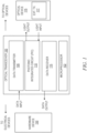
- FIG. 3 shows internal architecture 300 of an optical-electrical device 302, according to an example in which not every feature of the independent claims is explicitly depicted, but which is useful for highlighting specific aspects of the invention.
- the architecture 300 displays an optical-electrical device 302 that can send and receive optical data, such as optical transceiver 100.
- the optical-electrical device 302 comprises an electronics module 304 and a photonics module 307.
- the electronics module 304 includes electrical components (e.g., electrical conduction pathways/traces, circuit control logic, ASICs, processors, power control circuits, etc.), which can be integrated as one or more electrical structures or ASICs in a packaged chip, such as ASIC 215 of FIG. 2 .
- the electronics module 304 includes a transmitter controller 306 (e.g., data transmitter 105, FIG. 1 ) that receives data for optical modulation (e.g., PAM4 data, QPSK data).
- a hardware processor 305 e.g., a CPU, ASIC, microprocessor
- the electronics module 304 further includes a receiver controller 310 (e.g., data receiver 115), which can receive optical data generated by the optical receiver components in the photonics module 307.
- Electronics module 304 can further include a power control circuit 312 to supply and control electrical power for the optical-electrical device 302, including electronic components in the electronics module 304, and further supply electrical power to be photonics module 307 to power various electrically controlled photonic components (e.g., lasers, silicon optical amplifiers, filters, modulators, and so forth).
- a power control circuit 312 to supply and control electrical power for the optical-electrical device 302, including electronic components in the electronics module 304, and further supply electrical power to be photonics module 307 to power various electrically controlled photonic components (e.g., lasers, silicon optical amplifiers, filters, modulators, and so forth).
- the integrated photonics receiver structure 332 is an example of a WDM receiver that receives modulated WDM light (e.g., from an optical network) and processes the light by filtering, amplifying, and converting it to electrical signal using components such as multiplexers 334, semiconductor optical amplifiers (SOAs) 335, and one or more detectors such as photodetectors 336 (e.g., photodiodes).
- modulated WDM light e.g., from an optical network
- SOAs semiconductor optical amplifiers
- photodetectors 336 e.g., photodiodes
- the photonics module 307 can be fabricated in multiple processes, including first fabricating (e.g., using a mask or reticle) one or more silicon components followed by fabricating active components from III-V layers (e.g., using another mask or reticle).
- a second fabrication process forms additional components (e.g., active layer components in the photonics module 307 fabricated from III-V material), where the fabrication of the additional components can cause errors in the first components (e.g., trenching, damaged waveguides, bond interface damage).
- additional components e.g., active layer components in the photonics module 307 fabricated from III-V material
- damage can be indicated by optical loss by inputting light into the optical coupler 415A propagating through the waveguide to the optical coupler 415B and measuring the loss (e.g., loss greater than what is exepct4ed based on the light input).
- the optical fabrication monitor structure 415 is external to the photonic integrated circuit 412 and is not included in the final singulated die.
- one or more of the optical fabrication monitor structures are fabricated with an integrated light source and detector to generate light and detect the light in a self-contained approach (e.g., without having to input light into a coupler and receive the light from another coupler).
- the coupler 410A can be replaced with an integrated laser (e.g., hybrid laser formed partially from III-V material) and the coupler 410B can be replaced with an integrated photodiode to detect light generated by the integrated laser that propagates through the monitoring region (e.g., region A) via the health waveguide of the optical fabrication monitor structure 410.
- the laser and detector can be probed via electrical probing, which may be easier fabrication foundries to test using in-line standard electronic PCM electrical probe test, according to some example embodiments.
- the self-contained optical fabrication monitor structures do not require additional fabrication effort as they are formed as part of the same design as functional optical components of the photonic design, such as transceiver components of the photonics transmitter structure 314 (e.g., lasers, MZIs, EAMs) and receiver components of photonics receiver structure 332 (e.g., SOAs, detectors, etc.), as discussed above with reference to FIG. 3 .
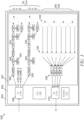
- FIG. 5 shows an example optical fabrication monitor architecture 500, according to an example in which not every feature of the independent claims is explicitly depicted, but which is useful for highlighting specific aspects of the invention.
- the fabrication reticle 505 is implemented to form a photonic layout design 515 on a wafer one or more times to create photonic designs on the wafer. Portions of the created photonic design is then singulated as separate photonic integrated circuits, such as photonic integrated circuit 510.
- the photonic integrated circuit 510 is an example implementation of the photonics module 307 or PIC 220, in which a portion of the components are fabricated using a first fabrication process (e.g.
- a second fabrication process forms additional components (e.g., active layer components in the photonics module 307 fabricated from III-V material), where the fabrication of the additional components can cause errors in the first components (e.g., trenching, damaged waveguides, bond interface damage).
- additional components e.g., active layer components in the photonics module 307 fabricated from III-V material
- the optical fabrication monitoring structure 520 can provide sub-decibel level detection of fabrication errors by detecting phase changes from an initial phase change (measured after the AMZI is created and before further fabrication cycle) or extinction ratio changes due to damage to a lower arm 545 that extends into the damage-susceptible area of region A of the photonics integrated circuit 510. After singulation of the photonics integrated circuit 510, a majority of the optical fabrication monitoring structure 520 is separated, and only the lower arm 545 is included with the separated photonic integrated circuit 510. Further, in some example embodiments, one or more of the optical fabrication monitoring structures of FIG. 5 is implemented as a self-contained optical fabrication monitor structures in which an integrated light source and/or detector is included in the monitor structure layout, as discussed above with reference to FIG. 4 .
- a second fabrication process forms additional components (e.g., active layer components in the photonics module 307 fabricated from III-V material), where the fabrication of the additional optical components can cause errors in the first components (e.g., trenching, damaged waveguides, bond interface damage).
- additional components e.g., active layer components in the photonics module 307 fabricated from III-V material
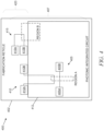
- the transmitter components include a laser 605, which is coupled to an optical modulator 610, which is coupled to an optical output coupler 615 of the transmitter.
- the transmitter optical fabrication test structure can detect losses or damage to the transmitter implementing a waveguide that is proximate to the transmitter portion of the photonic integrated circuit 612.
- the transmitter optical fabrication test structure can include test coupler 620 and 625 connected by a silicon waveguide that is designed as part of the layout to remain proximate to the transmitter path of the transmitter components.
- the transmitter portion can be tested and monitored by inputting light into the coupler 620 and detecting light by the coupler 625 and loss, which indicates potential damage to one or more components of the transmitter.
- the receiver can be tested in-line, the transmitter can be tested in-line, and the entire transceiver can be tested in-line without scrapping or contamination, thereby enabling early binning of parts and changes to fabrication processes or photonic layouts.
- one or more of the optical fabrication monitoring structures of FIG. 6 is implemented as a self-contained optical fabrication monitor structures in which an integrated light source and/or detector is included in the monitor structure layout, as discussed above with reference to FIG. 4 .
- a second set of components are created on the wafer (e.g., via a fabrication reticle).
- one or more of the components created during operation 705 may be damaged, as discussed above.
- the fabrication monitor optical structures to detect damage from one or more fabrication cycles, light is provided to the fabrication monitor optical structures, which is then received at operation 725.
- one or more errors are detected as indicated by the received light from the optical fabrication test structures. For example, received light can indicate that there is significant optical loss within one or more regions susceptible to fabrication damage. Further, damage can be detected based on the extinction ratio of an MZI test structure changing or increasing (e.g., increasing passed a designed or previous MZI extinction ratio.
- a first set of components can be formed in an initial fabrication cycle, where the first set includes functional components and monitor structures.
- a second set of components can be formed by subsequent fabrication processes that can potentially cause errors or damage to the first set of components.
- the monitor structures can be implemented during fabrication (e.g., in a cleanroom) to detect fabrication errors without pulling or scrapping the wafer.
Landscapes
- Physics & Mathematics (AREA)
- General Physics & Mathematics (AREA)
- Optics & Photonics (AREA)
- Analytical Chemistry (AREA)
- Chemical & Material Sciences (AREA)
- Microelectronics & Electronic Packaging (AREA)
- Engineering & Computer Science (AREA)
- Nonlinear Science (AREA)
- Health & Medical Sciences (AREA)
- Life Sciences & Earth Sciences (AREA)
- Biochemistry (AREA)
- General Health & Medical Sciences (AREA)
- Immunology (AREA)
- Pathology (AREA)
- Optical Integrated Circuits (AREA)
Applications Claiming Priority (1)
| Application Number | Priority Date | Filing Date | Title |
|---|---|---|---|
| US17/006,366 US11428646B2 (en) | 2020-08-28 | 2020-08-28 | Loss monitoring in photonic circuit fabrication |
Publications (3)
| Publication Number | Publication Date |
|---|---|
| EP3961276A1 EP3961276A1 (en) | 2022-03-02 |
| EP3961276C0 EP3961276C0 (en) | 2025-04-16 |
| EP3961276B1 true EP3961276B1 (en) | 2025-04-16 |
Family
ID=73497675
Family Applications (1)
| Application Number | Title | Priority Date | Filing Date |
|---|---|---|---|
| EP20208734.2A Active EP3961276B1 (en) | 2020-08-28 | 2020-11-19 | Loss monitoring in photonic circuit fabrication |
Country Status (6)
| Country | Link |
|---|---|
| US (1) | US11428646B2 (enExample) |
| EP (1) | EP3961276B1 (enExample) |
| JP (1) | JP7451376B2 (enExample) |
| KR (1) | KR102637475B1 (enExample) |
| CN (1) | CN114114539B (enExample) |
| TW (1) | TWI861281B (enExample) |
Families Citing this family (4)
| Publication number | Priority date | Publication date | Assignee | Title |
|---|---|---|---|---|
| US11428646B2 (en) | 2020-08-28 | 2022-08-30 | Openlight Photonics, Inc. | Loss monitoring in photonic circuit fabrication |
| US12181709B2 (en) | 2022-03-10 | 2024-12-31 | Ii-Vi Delaware, Inc. | Trimming of optical response for tunable photonic devices |
| US12699300B2 (en) * | 2023-02-24 | 2026-08-04 | Advanced Semiconductor Engineering, Inc. | Semiconductor devices |
| CN118330817B (zh) * | 2024-06-13 | 2024-10-15 | 杭州质禾科技有限公司 | 一种光芯片及其制备方法 |
Family Cites Families (26)
| Publication number | Priority date | Publication date | Assignee | Title |
|---|---|---|---|---|
| US5987196A (en) * | 1997-11-06 | 1999-11-16 | Micron Technology, Inc. | Semiconductor structure having an optical signal path in a substrate and method for forming the same |
| AU1799501A (en) * | 1999-11-23 | 2001-06-04 | Nanovation Technologies, Inc. | Optical mach-zehnder switch having a movable phase shifter |
| US6647350B1 (en) * | 2000-06-02 | 2003-11-11 | Exactus, Inc. | Radiometric temperature measurement system |
| ATE346410T1 (de) * | 2000-08-04 | 2006-12-15 | Amberwave Systems Corp | Siliziumwafer mit monolithischen optoelektronischen komponenten |
| US6767751B2 (en) * | 2002-05-28 | 2004-07-27 | Silicon Light Machines, Inc. | Integrated driver process flow |
| US7110629B2 (en) * | 2002-07-22 | 2006-09-19 | Applied Materials, Inc. | Optical ready substrates |
| US7402897B2 (en) * | 2002-08-08 | 2008-07-22 | Elm Technology Corporation | Vertical system integration |
| US6723573B2 (en) * | 2002-08-16 | 2004-04-20 | Sarnoff Corporation | Photonic devices and PICs including sacrificial testing structures and method of making the same |
| JP4141223B2 (ja) * | 2002-10-04 | 2008-08-27 | 日本電信電話株式会社 | 光回路及びその評価装置 |
| US20050016446A1 (en) * | 2003-07-23 | 2005-01-27 | Abbott John S. | CaF2 lenses with reduced birefringence |
| US7042657B2 (en) * | 2003-08-28 | 2006-05-09 | Board Of Regents The University Of Texas System | Filter for selectively processing optical and other signals |
| JP4457296B2 (ja) * | 2004-07-23 | 2010-04-28 | 三菱電機株式会社 | 光遅延回路、集積光素子および集積光素子の製造方法 |
| US20070002924A1 (en) * | 2005-06-30 | 2007-01-04 | Hutchinson John M | Integrated monitoring and feedback designs for external cavity tunable lasers |
| JP6206409B2 (ja) * | 2012-08-29 | 2017-10-04 | 日本電気株式会社 | 光集積回路、および光集積回路における光デバイスの検査方法 |
| JP2017524965A (ja) * | 2014-06-05 | 2017-08-31 | テクニオン・リサーチ・アンド・ディベロップメント・ファウンデーション・リミテッド | 大規模フォトニック集積回路の多自由度安定化 |
| US9354039B2 (en) * | 2014-06-06 | 2016-05-31 | Massachusetts Institute Of Technology | Methods, systems, and apparatus for programmable quantum photonic processing |
| WO2016033192A1 (en) | 2014-08-28 | 2016-03-03 | Adelos, Inc. | Noise management for optical time delay interferometry |
| CA3005704C (en) * | 2015-11-19 | 2020-12-01 | Nippon Telegraph And Telephone Corporation | Silicon optical circuit for detecting flaws in an optical circuit element based on light transmittance characteristics |
| US10613274B2 (en) * | 2016-05-13 | 2020-04-07 | Luxtera, Inc. | Method and system for integrated multi-port waveguide photodetectors |
| US10042131B1 (en) * | 2017-04-05 | 2018-08-07 | Xilinx, Inc. | Architecture for silicon photonics enabling wafer probe and test |
| US11131601B2 (en) * | 2017-11-30 | 2021-09-28 | Rain Tree Photonics Pte. Ltd. | Method for in-line optical testing |
| US10877300B2 (en) * | 2018-04-04 | 2020-12-29 | The Research Foundation For The State University Of New York | Heterogeneous structure on an integrated photonics platform |
| US10663282B1 (en) * | 2018-07-05 | 2020-05-26 | Lockheed Martin Corporation | Fiber-coupled phased array of photonic integrated circuit imagers |
| US11002763B2 (en) * | 2018-08-10 | 2021-05-11 | Globalfoundries U.S. Inc. | Probe for pic die with related test assembly and method |
| US10666353B1 (en) * | 2018-11-20 | 2020-05-26 | Juniper Networks, Inc. | Normal incidence photodetector with self-test functionality |
| US11428646B2 (en) | 2020-08-28 | 2022-08-30 | Openlight Photonics, Inc. | Loss monitoring in photonic circuit fabrication |
-
2020
- 2020-08-28 US US17/006,366 patent/US11428646B2/en active Active
- 2020-10-23 JP JP2020177748A patent/JP7451376B2/ja active Active
- 2020-11-12 TW TW109139472A patent/TWI861281B/zh active
- 2020-11-18 CN CN202011294845.8A patent/CN114114539B/zh active Active
- 2020-11-18 KR KR1020200154837A patent/KR102637475B1/ko active Active
- 2020-11-19 EP EP20208734.2A patent/EP3961276B1/en active Active
Also Published As
| Publication number | Publication date |
|---|---|
| CN114114539A (zh) | 2022-03-01 |
| KR20220029276A (ko) | 2022-03-08 |
| EP3961276A1 (en) | 2022-03-02 |
| TW202214997A (zh) | 2022-04-16 |
| JP2022039883A (ja) | 2022-03-10 |
| KR102637475B1 (ko) | 2024-02-19 |
| JP7451376B2 (ja) | 2024-03-18 |
| TWI861281B (zh) | 2024-11-11 |
| CN114114539B (zh) | 2023-04-18 |
| US20220065798A1 (en) | 2022-03-03 |
| EP3961276C0 (en) | 2025-04-16 |
| US11428646B2 (en) | 2022-08-30 |
Similar Documents
| Publication | Publication Date | Title |
|---|---|---|
| US11428646B2 (en) | Loss monitoring in photonic circuit fabrication | |
| US10721035B2 (en) | Method and system for an optoelectronic built-in self-test system for silicon photonics optical transceivers | |
| Gunn | CMOS photonics for high-speed interconnects | |
| US11012152B2 (en) | Method and system for connectionless integrated optical receiver and transmitter test | |
| US10042131B1 (en) | Architecture for silicon photonics enabling wafer probe and test | |
| JP7480029B2 (ja) | オンチップフォトニック集積回路光学検証 | |
| De Dobbelaere et al. | Advanced silicon photonics technology platform leveraging a semiconductor supply chain | |
| CN114062798A (zh) | 用于光电器件的测试的混合自动测试设备 | |
| TWI773248B (zh) | 半導體結構及其形成方法 | |
| CN110161634A (zh) | 光电芯片以及用于测试这种芯片的光子电路的方法 | |
| JP6823571B2 (ja) | 光回路 | |
| Gunn | Fully integrated VLSI CMOS and photonics" CMOS photonics" | |
| JP6225072B2 (ja) | 半導体mz光変調器および半導体mz光変調器を用いた方法 | |
| Bernabé et al. | Packaging of photonic integrated circuit based high-speed coherent transmitter module | |
| Chen et al. | Characterization of Silicon Photonics Modulator Integration and High Efficiency Testing Platform | |
| Dasgupta | Silicon Photonic Failure Analysis Using Near Infrared Microscopy |
Legal Events
| Date | Code | Title | Description |
|---|---|---|---|
| PUAI | Public reference made under article 153(3) epc to a published international application that has entered the european phase |
Free format text: ORIGINAL CODE: 0009012 |
|
| STAA | Information on the status of an ep patent application or granted ep patent |
Free format text: STATUS: THE APPLICATION HAS BEEN PUBLISHED |
|
| AK | Designated contracting states |
Kind code of ref document: A1 Designated state(s): AL AT BE BG CH CY CZ DE DK EE ES FI FR GB GR HR HU IE IS IT LI LT LU LV MC MK MT NL NO PL PT RO RS SE SI SK SM TR |
|
| STAA | Information on the status of an ep patent application or granted ep patent |
Free format text: STATUS: REQUEST FOR EXAMINATION WAS MADE |
|
| 17P | Request for examination filed |
Effective date: 20220901 |
|
| RBV | Designated contracting states (corrected) |
Designated state(s): AL AT BE BG CH CY CZ DE DK EE ES FI FR GB GR HR HU IE IS IT LI LT LU LV MC MK MT NL NO PL PT RO RS SE SI SK SM TR |
|
| RAP1 | Party data changed (applicant data changed or rights of an application transferred) |
Owner name: OPENLIGHT PHOTONICS, INC. |
|
| GRAP | Despatch of communication of intention to grant a patent |
Free format text: ORIGINAL CODE: EPIDOSNIGR1 |
|
| STAA | Information on the status of an ep patent application or granted ep patent |
Free format text: STATUS: GRANT OF PATENT IS INTENDED |
|
| RIC1 | Information provided on ipc code assigned before grant |
Ipc: G02B 6/13 20060101ALI20241021BHEP Ipc: G01M 11/00 20060101ALI20241021BHEP Ipc: G02B 6/12 20060101AFI20241021BHEP |
|
| INTG | Intention to grant announced |
Effective date: 20241112 |
|
| GRAS | Grant fee paid |
Free format text: ORIGINAL CODE: EPIDOSNIGR3 |
|
| GRAA | (expected) grant |
Free format text: ORIGINAL CODE: 0009210 |
|
| STAA | Information on the status of an ep patent application or granted ep patent |
Free format text: STATUS: THE PATENT HAS BEEN GRANTED |
|
| AK | Designated contracting states |
Kind code of ref document: B1 Designated state(s): AL AT BE BG CH CY CZ DE DK EE ES FI FR GB GR HR HU IE IS IT LI LT LU LV MC MK MT NL NO PL PT RO RS SE SI SK SM TR |
|
| REG | Reference to a national code |
Ref country code: GB Ref legal event code: FG4D |
|
| REG | Reference to a national code |
Ref country code: CH Ref legal event code: EP |
|
| REG | Reference to a national code |
Ref country code: IE Ref legal event code: FG4D |
|
| REG | Reference to a national code |
Ref country code: DE Ref legal event code: R096 Ref document number: 602020049475 Country of ref document: DE |
|
| U01 | Request for unitary effect filed |
Effective date: 20250506 |
|
| U07 | Unitary effect registered |
Designated state(s): AT BE BG DE DK EE FI FR IT LT LU LV MT NL PT RO SE SI Effective date: 20250512 |
|
| PG25 | Lapsed in a contracting state [announced via postgrant information from national office to epo] |
Ref country code: ES Free format text: LAPSE BECAUSE OF FAILURE TO SUBMIT A TRANSLATION OF THE DESCRIPTION OR TO PAY THE FEE WITHIN THE PRESCRIBED TIME-LIMIT Effective date: 20250416 |
|
| PG25 | Lapsed in a contracting state [announced via postgrant information from national office to epo] |
Ref country code: GR Free format text: LAPSE BECAUSE OF FAILURE TO SUBMIT A TRANSLATION OF THE DESCRIPTION OR TO PAY THE FEE WITHIN THE PRESCRIBED TIME-LIMIT Effective date: 20250717 Ref country code: NO Free format text: LAPSE BECAUSE OF FAILURE TO SUBMIT A TRANSLATION OF THE DESCRIPTION OR TO PAY THE FEE WITHIN THE PRESCRIBED TIME-LIMIT Effective date: 20250716 |
|
| PG25 | Lapsed in a contracting state [announced via postgrant information from national office to epo] |
Ref country code: PL Free format text: LAPSE BECAUSE OF FAILURE TO SUBMIT A TRANSLATION OF THE DESCRIPTION OR TO PAY THE FEE WITHIN THE PRESCRIBED TIME-LIMIT Effective date: 20250416 |
|
| PG25 | Lapsed in a contracting state [announced via postgrant information from national office to epo] |
Ref country code: HR Free format text: LAPSE BECAUSE OF FAILURE TO SUBMIT A TRANSLATION OF THE DESCRIPTION OR TO PAY THE FEE WITHIN THE PRESCRIBED TIME-LIMIT Effective date: 20250416 |
|
| PG25 | Lapsed in a contracting state [announced via postgrant information from national office to epo] |
Ref country code: RS Free format text: LAPSE BECAUSE OF FAILURE TO SUBMIT A TRANSLATION OF THE DESCRIPTION OR TO PAY THE FEE WITHIN THE PRESCRIBED TIME-LIMIT Effective date: 20250716 |
|
| PG25 | Lapsed in a contracting state [announced via postgrant information from national office to epo] |
Ref country code: IS Free format text: LAPSE BECAUSE OF FAILURE TO SUBMIT A TRANSLATION OF THE DESCRIPTION OR TO PAY THE FEE WITHIN THE PRESCRIBED TIME-LIMIT Effective date: 20250816 |
|
| U20 | Renewal fee for the european patent with unitary effect paid |
Year of fee payment: 6 Effective date: 20251113 |
|
| PG25 | Lapsed in a contracting state [announced via postgrant information from national office to epo] |
Ref country code: SM Free format text: LAPSE BECAUSE OF FAILURE TO SUBMIT A TRANSLATION OF THE DESCRIPTION OR TO PAY THE FEE WITHIN THE PRESCRIBED TIME-LIMIT Effective date: 20250416 |
|
| PG25 | Lapsed in a contracting state [announced via postgrant information from national office to epo] |
Ref country code: CZ Free format text: LAPSE BECAUSE OF FAILURE TO SUBMIT A TRANSLATION OF THE DESCRIPTION OR TO PAY THE FEE WITHIN THE PRESCRIBED TIME-LIMIT Effective date: 20250416 |
|
| PG25 | Lapsed in a contracting state [announced via postgrant information from national office to epo] |
Ref country code: SK Free format text: LAPSE BECAUSE OF FAILURE TO SUBMIT A TRANSLATION OF THE DESCRIPTION OR TO PAY THE FEE WITHIN THE PRESCRIBED TIME-LIMIT Effective date: 20250416 |
|
| PLBE | No opposition filed within time limit |
Free format text: ORIGINAL CODE: 0009261 |
|
| STAA | Information on the status of an ep patent application or granted ep patent |
Free format text: STATUS: NO OPPOSITION FILED WITHIN TIME LIMIT |
|
| REG | Reference to a national code |
Ref country code: CH Ref legal event code: L10 Free format text: ST27 STATUS EVENT CODE: U-0-0-L10-L00 (AS PROVIDED BY THE NATIONAL OFFICE) Effective date: 20260225 |
|
| 26N | No opposition filed |
Effective date: 20260119 |
|
| REG | Reference to a national code |
Ref country code: CH Ref legal event code: H13 Free format text: ST27 STATUS EVENT CODE: U-0-0-H10-H13 (AS PROVIDED BY THE NATIONAL OFFICE) Effective date: 20260623 |
|
| PG25 | Lapsed in a contracting state [announced via postgrant information from national office to epo] |
Ref country code: MC Free format text: LAPSE BECAUSE OF FAILURE TO SUBMIT A TRANSLATION OF THE DESCRIPTION OR TO PAY THE FEE WITHIN THE PRESCRIBED TIME-LIMIT Effective date: 20250416 |
|
| PG25 | Lapsed in a contracting state [announced via postgrant information from national office to epo] |
Ref country code: CH Free format text: LAPSE BECAUSE OF NON-PAYMENT OF DUE FEES Effective date: 20251130 |