EP3958467B1 - Schaltermodul, treiberschaltung und verfahren - Google Patents
Schaltermodul, treiberschaltung und verfahren Download PDFInfo
- Publication number
- EP3958467B1 EP3958467B1 EP20191782.0A EP20191782A EP3958467B1 EP 3958467 B1 EP3958467 B1 EP 3958467B1 EP 20191782 A EP20191782 A EP 20191782A EP 3958467 B1 EP3958467 B1 EP 3958467B1
- Authority
- EP
- European Patent Office
- Prior art keywords
- terminal
- short circuit
- switch
- transistor
- load
- Prior art date
- Legal status (The legal status is an assumption and is not a legal conclusion. Google has not performed a legal analysis and makes no representation as to the accuracy of the status listed.)
- Active
Links
Images



Classifications
-
- H—ELECTRICITY
- H03—ELECTRONIC CIRCUITRY
- H03K—PULSE TECHNIQUE
- H03K17/00—Electronic switching or gating, i.e. not by contact-making and –breaking
- H03K17/08—Modifications for protecting switching circuit against overcurrent or overvoltage
- H03K17/082—Modifications for protecting switching circuit against overcurrent or overvoltage by feedback from the output to the control circuit
-
- H—ELECTRICITY
- H03—ELECTRONIC CIRCUITRY
- H03K—PULSE TECHNIQUE
- H03K17/00—Electronic switching or gating, i.e. not by contact-making and –breaking
- H03K17/08—Modifications for protecting switching circuit against overcurrent or overvoltage
- H03K17/082—Modifications for protecting switching circuit against overcurrent or overvoltage by feedback from the output to the control circuit
- H03K17/0822—Modifications for protecting switching circuit against overcurrent or overvoltage by feedback from the output to the control circuit in field-effect transistor switches
-
- H—ELECTRICITY
- H03—ELECTRONIC CIRCUITRY
- H03K—PULSE TECHNIQUE
- H03K17/00—Electronic switching or gating, i.e. not by contact-making and –breaking
- H03K17/08—Modifications for protecting switching circuit against overcurrent or overvoltage
- H03K17/081—Modifications for protecting switching circuit against overcurrent or overvoltage without feedback from the output circuit to the control circuit
- H03K17/0812—Modifications for protecting switching circuit against overcurrent or overvoltage without feedback from the output circuit to the control circuit by measures taken in the control circuit
- H03K17/08128—Modifications for protecting switching circuit against overcurrent or overvoltage without feedback from the output circuit to the control circuit by measures taken in the control circuit in composite switches
-
- H—ELECTRICITY
- H03—ELECTRONIC CIRCUITRY
- H03K—PULSE TECHNIQUE
- H03K17/00—Electronic switching or gating, i.e. not by contact-making and –breaking
- H03K17/08—Modifications for protecting switching circuit against overcurrent or overvoltage
- H03K17/081—Modifications for protecting switching circuit against overcurrent or overvoltage without feedback from the output circuit to the control circuit
- H03K17/0812—Modifications for protecting switching circuit against overcurrent or overvoltage without feedback from the output circuit to the control circuit by measures taken in the control circuit
- H03K17/08122—Modifications for protecting switching circuit against overcurrent or overvoltage without feedback from the output circuit to the control circuit by measures taken in the control circuit in field-effect transistor switches
-
- H—ELECTRICITY
- H03—ELECTRONIC CIRCUITRY
- H03K—PULSE TECHNIQUE
- H03K17/00—Electronic switching or gating, i.e. not by contact-making and –breaking
- H03K17/08—Modifications for protecting switching circuit against overcurrent or overvoltage
- H03K17/082—Modifications for protecting switching circuit against overcurrent or overvoltage by feedback from the output to the control circuit
- H03K17/0828—Modifications for protecting switching circuit against overcurrent or overvoltage by feedback from the output to the control circuit in composite switches
-
- H—ELECTRICITY
- H03—ELECTRONIC CIRCUITRY
- H03K—PULSE TECHNIQUE
- H03K2217/00—Indexing scheme related to electronic switching or gating, i.e. not by contact-making or -breaking covered by H03K17/00
- H03K2217/0027—Measuring means of, e.g. currents through or voltages across the switch
Definitions
- the present application relates to switch modules, driver circuits for switch modules, systems including a driver circuit and a switch module and to corresponding methods.
- Power transistor based switches are used in various applications to switch high currents or high voltages, for example to selectively couple a load to a power source like a supply voltage.
- Such switches may be provided with single power transistors, or as combinations of transistor and diode (for example an insulated gate bipolar transistor, IGBT, with anti-parallel freewheeling diode) or as combinations of several transistors, for example two power transistors in a half bridge configuration. Other combinations are also possible.
- Power transistors may be made up of a plurality of transistor cells coupled in series or in parallel to support high currents, for example several amperes, or high voltages.
- a short circuit may refer to a condition where the power transistors, in a switched on state, couples a very small load (e.g. only a few Ohms) to a power supply, for example a short circuit by a simple wire or other metal connection).
- a very small load e.g. only a few Ohms
- the current flowing through the power transistor can become very large, leading for example to heating or damaging of the power transistor.
- other parts of an electronic circuit may be damaged by the high current.
- desaturation detection For insulated gate bipolar transistors, a conventional approach for short circuit monitoring is referred to as desaturation (desat) detection. This, however, may be too slow in some cases, i.e. detection of the short circuit and subsequent switching off of the power transistor may take too long. Furthermore, this approach may limit performance of the power transistor and requires additional components outside a package of the power transistor like diodes, which require space and may lead to parasitic effects.
- EP0561386 A1 and US 2001/026429 A1 disclose semiconductor devices which include an overcurrent limiting protection.
- a switch module as defined in claim 1, a driver circuit as defined in claim 7 and a method as defined in Claim 14 are provided.
- the dependent claims defined further embodiments as well as systems including a switch module and a driver circuit.
- a switch module is a device including one or more transistor switches.
- a switch module may be provided as a single package, with a single housing or integrated on a single chip. For example, one or more chips may be provided in a single package.
- a transistor switch is a switch based on a transistor or several transistors.
- the transistor may be a power transistor designed for switching high currents or voltages, for example currents of several amperes or voltages of several 10 V or even 100 V or above.
- the transistor switch may also be designed for lower voltages or currents, depending on the application.
- the term "switch" in transistor switch refers to the fact that the transistor switch is intended to be used as a switch in either an on state or an off state, for example in contrast to transistors used in a linear range.
- Transistor switches as mentioned already in the background may be made up of a plurality of transistor cells coupled in series or in parallel.
- Transistor switches are described as comprising a control terminal, a first load terminal and a second load terminal. By applying a control signal to the control terminal, the transistor switch may be switched on or off.
- a transistor switch is switched on or in an on-state when it provides a low-ohmic connection between its first and second load terminal, and is switched off when it essentially provides an electric isolation (apart from very small leakage currents, which may occur in real implementations) between its first and second load terminals.
- transistors may be used for transistor switches. Examples include field effect transistors (FETs) like metal oxide semiconductor field effect transistors (MOSFETs), bipolar junction transistors (BJTs) or insulated gate bipolar transistors (IGBTs). Transistors may be based on various semiconductor materials like Silicon (Si), Silicon Carbide (SiC) or III-V compounds like Gallium Arsenide. For example, a SiC MOSFET may be used in some embodiments.
- FETs field effect transistors
- MOSFETs metal oxide semiconductor field effect transistors
- BJTs bipolar junction transistors
- IGBTs insulated gate bipolar transistors
- Transistors may be based on various semiconductor materials like Silicon (Si), Silicon Carbide (SiC) or III-V compounds like Gallium Arsenide.
- SiC MOSFET may be used in some embodiments.
- the control terminal is a gate terminal, the first load terminal is a source terminal and the second load terminal is a drain terminal.
- the control terminal is a base terminal, the first load terminal is an emitter terminal and the second load terminal is a collector terminal.
- the control terminal is a gate terminal, the first load terminal is an emitter terminal and the second load terminal is a collector terminal.
- the switch module may include a single transistor switch, but may also include more than one transistor switch, for example two transistor switches in a half bridge or other configuration. In other embodiments, more than two transistor switches, for example four or six transistor switches, may be provided, which may be arranged in pairs to form half bridge configurations, for example for driving different phases of an electric motor. Different transistor switches in a switch module may be of the same type or of different types (for example only IGBTs, or a MOSFET together with an IGBT, etc.). In the following, for ease of explanations, switch modules with a single transistor switch will be discussed. However, it is to be understood that the techniques discussed herein are also applicable to switch modules including more than one transistor switches. In this sense, the reference to "a transistor switch" as used herein is to be construed as referring to one or more transistor switches.
- a control signal for turning a transistor switch of a switch module on or off may be supplied by a driver circuit.
- a driver circuit may be provided separately to the switch module, for example on a separate chip, in a separate housing, integrated within another electronic circuit etc.
- Fig. 1A illustrates a system according to an embodiment including a switch module 10 and a driver circuit 13. Such a system may be referred to as an intelligent power module.
- Switch module 10 comprises a transistor switch 11.
- Transistor switch 11 in the example of Fig. 1A is an insulated gate bipolar transistor (IGBT) with a freewheeling diode. As mentioned above, this is given only as an example, and other types of transistor switches and/or more than one transistor switch may be provided in a switch module 10, for example a SiC-based MOSFET.
- IGBT insulated gate bipolar transistor
- a gate terminal of transistor switch 11 is coupled to an external gate terminal G of switch module 10, a collector terminal of transistor switch 11 is coupled to an external collector terminal C of switch module 10 and an emitter terminal of transistor switch 11 is coupled to an external emitter terminal E and an external auxiliary emitter terminal E' of switch module 10.
- External terminals G, C, E and E' are "external" terminals of switch module 10 in the sense that via these terminals switch module 10 may be coupled to other devices. Such external terminals may for example be realized as pins of a package.
- external terminals G, C, E and E' are the only external terminals of switch module 10, or, more generally speaking, all external terminals of switch module 10 are coupled to the low terminals or control terminals of the transistor switch or transistor switches of switch module 10 (in this case to gate, collector and emitter terminals of transistor switch 11).
- no separate terminals for supplying a short detection circuit 12 to be described later or additional terminals for outputting a signal indicating a short circuit are provided.
- additional measurement circuitry for example a temperature measurement device like a temperature dependent resistor or thermistor, may be provided in switch module 10 and accessed via separate external terminals.
- Such separate external terminals if provided, in some embodiments are independent from the terminals related to the components shown in Fig. 1A and in particular are not related to the short circuit detection described herein.
- external collector terminal C may be coupled to a supply voltage
- external emitter terminal E may be coupled to a load.
- a control signal CTRLCTRL is supplied to driver circuit 13, which controls transistor switch 11 by applying a corresponding gate signal at external terminal G via a gate resistor R G, ext such that a corresponding gate emitter voltage (between terminals G and E') switches transistor switch 11 on or off, as demanded by control signal CTRL.
- Driver circuit 13 in the embodiment of Fig. 1A is supplied by positive supply voltages V CC1 , V CC2 .
- switch module 10 comprises a short circuit detection circuit 12.
- short circuit detection circuit 12 receives an indication of a current through transistor switch 11 via a line 17.
- An indication of the current refers to any signal indicative of the current through transistor switch 11.
- load current short circuit detection circuit 12 detects whether a short circuit state is present at the load terminals of switch module 10.
- a short circuit state for example would be present if collector terminal C is connected to a supply voltage, and then emitter terminal E is short-circuited to ground, i.e. connected to ground via a low ohmic connection like a wire or other comparatively low resistance.
- a short circuit state in this sense may still include some resistance, for example a resistance of a few Ohms.
- a short circuit state refers to a condition which could cause higher currents through transistor switch 11 than transistor switch 11 is designed for.
- Short circuit detection circuit 12 may for example detect a short circuit state by comparing the indication by the current received to a threshold value, and if the comparison shows that the current exceeds the threshold, this corresponds to a short circuit detection. In other embodiments, a short circuit state may be detected if the indication indicates a fast rising current.
- short circuit detection circuit 12 electrically couples a line 16 connected to the gate terminal of transistor switch 11 to a line 15 coupled to the emitter terminal of switch device 11. This electric coupling causes a gate emitter voltage to drop, which switches switch 11 off.
- Such an electric coupling between lines 15, 16 may essentially short-circuit in lines 15, 16 or may couple lines 15, 16 with a resistor sufficiently low-ohmic to allow the drop of the gate emitter voltage.
- short circuit detection circuit 12 does not receive a separate supply voltage, which would for example have to be supplied via additional external terminals of switch module 10, but is supplied by the gate emitter voltage via lines 15, 16.
- transistor switch 11 when the gate emitter voltage is low, transistor switch 11 is off, such that no short circuit monitoring is required (as transistor switch 11 is switched off anyway).
- switch transistor switch 11 on a sufficiently high gate emitter voltage has to be supplied, which then is able to also supply short circuit detection circuit 12.
- Fig. 1B shows a system according to a further embodiment, which is a variation of the system of Fig. 1B .
- Fig. 1A also apply to Fig. 1B
- corresponding elements bear the same reference numerals and will not be described again.
- Switch module 10 of Fig. 1B comprises an external auxiliary collector terminal C' coupled to the collector terminal of switch transistor 11.
- Driver circuit 13 is coupled to external auxiliary collector terminal C' via a resistor R DESAT and a Diode D DESAT .
- a capacitor C DESAT is coupled as shown between Resistor R DESAT and external auxiliary emitter terminal E'. As will be explained further below, this in some embodiments allows a conventional desaturation based short circuit detection by driver circuit 13.
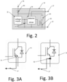
- short circuit detection circuit 12 An example implementation of short circuit detection circuit 12 is illustrated in Fig. 2 . Other implementations are also possible.
- short circuit detection circuit 12 includes a diode 20 coupled to line 16 which prevents reverse currents.
- Line 16 is coupled to a voltage supply 21 which provides a voltage to a detector/driver circuit 23, when the gate emitter voltage between lines 16 and 15 is large enough, for example at least in the range of a threshold voltage necessary for switching transistor switch 11 on.
- a buffer capacitor 22 is coupled between voltage supply 21 and detector/driver circuit 23.
- Detector/driver circuit 23 receives the indication of the current from line 17 to detect the short circuit state.
- detector/driver circuit 23 may include a comparator to compare the indication of the current to a threshold value, and if the threshold value is exceeded, a short circuit is detected. Additionally or alternatively, detector/driver circuit 23 may include a differentiator in combination with a comparator, to detect fast increases of the current, in a range typical for a short circuit. When a short circuit is detected, detector/driver circuit controls a transistor 25 to be switched on, which couples lines 16, 15 and therefore, gate and emitter terminals of transistor switch 11, via a resistor 24.
- Resistor 24 may for example have a resistance value such that the gate emitter voltage drops in case of a short circuit and transistor switch 11 is switched off.
- the resistance value may be selected depending on gate resistor R G , ext , an on-resistance R ds, on of transistor 25 and an internal resistance of driver 13 such that when transistor 25 is switched on, the gate-emitter voltage of transistor switch 11 is lower than the threshold voltage of transistor switch 11, but high enough for voltage supply 21 to still receive sufficient voltage to maintain operation of short circuit detection circuit 12.
- driver circuit 13 in some embodiments may include an additional short circuit detection.
- short circuit detection 12 enables a short reaction time for short circuit detection, for example below 2 ⁇ s, to switch off transistor switch 11 quickly. After some more time, for example 5 ms, the short circuit driver circuit 13 "takes over".
- driver circuit 13 need not include a short circuit detection.
- Fig. 3A shows a case where a sense transistor is used to sense the current.
- a small proportion of the active area of transistor switch 11 is provided as separate emitter terminal (or source terminal in the case of field effect transistors) such that via line 17 a current proportional to the current between external collector terminal C and external emitter terminal E, but much smaller, is provided. Any conventional implementations of such sense transistors may be used.
- the current thus provided on line 17 may then be measured by detector/driver circuit 23, for example as a voltage drop over a measurement resistor.
- Fig. 3B shows a contactless measurement device 32 for measuring the current.
- Such contactless measurement devices may for example measure the current based on a magnetic field generated by the current.
- the measurement device may include a Hall sensor, a magnetoresistive sensor or any other kind of magnetic field sensor.
- a signal representing the magnetic field thus sensed, which may be proportional to the current, is provided on line 17 and then evaluated in detector/driver circuit 23.
- a measurement resistor 33 is coupled in series to the transistor of transistor switch 11, and a voltage job over resistor 33 is provided on line 17 as indication of the current. This approach is for example applicable to low power application.
- Fig. 3A to 3C show, various approaches for obtaining the indication of the current may be used.
- driver circuit 13 includes various features which may be used independently, but also in combination, are shown in Figs. 5A and 5B .
- driver circuit 13 may operate as and be implemented as a conventional driver circuit for driving transistor switches.
- driver circuit 13 may include a push-pull-driver including transistors T1, T2 and a controller 52 driving transistors T1, T2 based on control signal CTRL to output a signal to gate terminal G.
- driver circuit 13 provides short circuit detection.
- a conventional driver circuit using short circuit detection based on desaturation may be used.
- such a desaturation based detection is performed using a current source 50 providing a current I DESAT and a comparator 51 receiving, at one input, the current I DESAT combined with a signal from auxiliary emitter terminal C' of switch device 10 via diode D DESAT and resistor R DESAT as shown in Fig. 1B , and, at another input, a reference voltage V REF_DESAT .
- a short circuit is detected based on a temporary voltage rise between the external auxiliary collector terminal C' and the external auxiliary emitter terminal E'.
- controller 52 Based on an output of comparator 51, controller 52 detects a short circuit and switches off transistor switch 11 in response to the detection of a short circuit.
- the additional circuit elements of Fig. 1B i.e. diode D DESAT , resistor R DESAT and capacitor C DESAT are required.
- a driver circuit 13 instead of a conventional driver circuit 13, a driver circuit 13 according to an embodiment is provided, which again contains a conventional driver like a push-pull driver with transistors T1, T2 for driving transistor switch 11 in normal operation. However, unlike conventional driver circuits, such a driver circuit uses signals at gate terminal G and/or auxiliary emitter terminal E' for short circuit detection.
- controller 52 of driver circuit 13 monitors the current flowing from driver circuit 13 to external gate terminal G of switch module 10 using a current meter 53.
- short circuit detection circuit 12 provides the electrical connection between lines 16 and 15 in case of a short circuit, an increased current flows from gate terminal G to emitter terminal E or auxiliary emitter terminal E'.
- driver circuit 13 This increased current flow to gate terminal G is provided by driver circuit 13 and may be measured by driver circuit 13.
- Any conventional current measurement techniques for example contactless methods as described with reference to Fig. 3B or a shunt resistor as described with reference to Fig. 3C , are also a sense transistor, depending on the design of driver circuit 13, may be used as current meter 53.
- the current detection may be made at the corresponding terminal of driver circuit 13 or at internal circuit components, for example driver components, of driver circuit 13.
- the thus sensed current may be compared to a threshold, for example by a comparator, and when the current exceeds the threshold, a short circuit is detected and the control signal to gate terminal G is set to switch transistor switch 11 off.
- the short circuit may be detected by controller 52 monitoring the voltage between gate terminal G and auxiliary emitter terminal E' using a voltage meter 54.
- short circuit detection circuit 12 detects a short circuit and provides the electrical connection between lines 16 and 15, due to this connection there is a dip, i.e. at an at least temporary decrease, in the voltage between gate terminal G and emitter terminal E'.
- This voltage dip may be detected by driver circuit 13, for example by continuously measuring the voltage.
- voltage meter 54 for example an analog to digital converter may be used, and the measured voltage may then be evaluated digitally.
- driver circuit 13 of Fig. 5A implements both desaturation based short circuit detection and gate current based short circuit detection
- driver circuit 13 of Fig. 5B implements both desaturation based short circuit detection and gate-emitter voltage based short circuit detection.
- the desaturation based short circuit detection i.e. components 50, 51 and terminal C'
- a corresponding driver circuit may then be used e.g. in the system of Fig. 1A .
- Other combinations are also possible.
- Fig. 4 is a flow chart illustrating a method according to some embodiments.
- the method of Fig. 4 may be implemented in the systems, switch modules and driver circuits discussed above, and in order to avoid repetitions will be described with respect to the previous explanations. However, the method of Fig. 4 may also be implemented in other systems, switch modules and driver circuits than the ones explained above.
- the method comprises driving a switch module, i.e. driving one or more transistors switches of a switch module to switch them on and off.
- the method comprises detecting a short circuit by the switch module.
- the short circuit is detected within the switch module and not by an external entity like a driver circuit.
- the short circuit may be detected by short circuit detection circuit 12 described previously.
- the method in response to detecting the short circuit, includes electrically coupling a control terminal of a transistor switch of the switch module to a first load terminal of the transistor switch, in the example of Fig. 1 by electrically coupling lines 16 and 15. This turns off the transistor switch at least temporarily.
- the method comprises detecting the short circuit also by a driver circuit, for example driver circuit 13 as discussed previously.
- the driver circuit controls switches of the switch modules, i.e. controls one or more transistor switches of the switch module to be switched off.
Landscapes
- Electronic Switches (AREA)
- Power Conversion In General (AREA)
Claims (14)
- Schaltmodul (10), umfassend:einen Transistorschalter (11) mit einem Steueranschluss,einem ersten Lastanschluss und einem zweiten Lastanschluss,eine Kurzschlussdetektionsschaltung (12), die konfiguriert ist, um einen Kurzschlusszustand zwischen dem ersten Lastanschluss und dem zweiten Lastanschluss zu detektieren und um den Transistorschalter (11) durch Einschalten eines Transistors (25) , um den Steueranschluss mit dem ersten Lastanschluss als Reaktion auf das Detektieren des Kurzschlusszustands elektrisch zu koppeln, auszuschalten,wobei die Kurzschlussdetektionsschaltung (12) konfiguriert ist, um durch eine zwischen dem Steueranschluss und dem ersten Lastanschluss angelegte Spannung mit Strom versorgt zu werden, wenn die zwischen dem Steueranschluss und dem ersten Lastanschluss angelegte Spannung hoch genug ist, um den Transistorschalter (11) einzuschalten,wobei die Kurzschlussdetektionsschaltung (12) konfiguriert ist, um einen Strom durch den Transistorschalter (11) zwischen dem ersten und dem zweiten Lastanschluss zu messen und um den Kurzschlusszustand zu detektieren, wenn der Strom einen vordefinierten Schwellenwert überschreitet.
- Schaltmodul (10) nach Anspruch 1,
wobei die Kurzschlussdetektionsschaltung (12) konfiguriert ist, um kein zusätzliches Signal auszugeben, das die Detektion des Kurzschlusszustands anzeigt. - Schaltmodul (10) nach Anspruch 1 oder 2, wobei der Transistorschalter (11) einen Siliziumcarbid-basierten Metalloxid-Halbleiter-Feldeffekttransistor umfasst, wobei der Steueranschluss ein Gate-Anschluss ist, der erste Lastanschluss ein Source-Anschluss ist und der zweite Lastanschluss ein Drain-Anschluss des Siliziumcarbid-basierten Metalloxid-Halbleiter-Feldeffekttransistors ist.
- Schaltmodul (10) nach einem der Ansprüche 1 bis 3, wobei der Transistorschalter (11) einen Bipolartransistor mit isoliertem Gate umfasst, wobei der Steueranschluss ein Gate-Anschluss ist, der erste Lastanschluss ein Emitter-Anschluss ist und der zweite Lastanschluss ein Kollektor-Anschluss des Bipolartransistors mit isoliertem Gate ist.
- Schaltmodul (10) nach Anspruch 4, wobei alle externen Anschlüsse (G, E, C, E', C') des Schaltmoduls (10), die mit dem Transistorschalter (11) oder der Kurzschlussdetektionsschaltung (12) gekoppelt sind, ausgewählt sind aus der Gruppe bestehend aus:einem Haupt-Gate-Anschluss (G), der mit dem Gate-Anschluss gekoppelt ist,einem Haupt-Emitter-Anschluss (E), der mit dem Emitter-Anschluss gekoppelt ist,einem Haupt-Kollektor-Anschluss (C), der mit dem Kollektor-Anschluss gekoppelt ist,einem Hilfs-Emitter-Anschluss (E'), der mit dem Emitter-Anschluss gekoppelt ist,einem Hilfs-Kollektor-Anschluss (C'), der mit dem Kollektor-Anschluss gekoppelt ist.
- System, umfassend:das Schaltmodul (10) nach einem der Ansprüche 1-5, undeine Treiberschaltung (13), wobei die Treiberschaltung (13) konfiguriert ist, um ein Steuersignal an einen Steueranschluss des Schaltmoduls (10) zum Steuern des Transistorschalters (11) bereitzustellen, um einen Kurzschlusszustand zwischen einem ersten und einem zweiten Lastanschluss des Schaltmoduls (10) zu detektieren und um den Transistorschalter (11) als Reaktion auf das Detektieren des Kurzschlusses auszuschalten.
- System nach Anspruch 6, wobei die Treiberschaltung (13) konfiguriert ist, um den Kurzschlusszustand auf der Grundlage eines Spannungsanstiegs zwischen dem ersten und dem zweiten Lastanschluss zu detektieren.
- System nach Anspruch 6 oder 7, wobei die Treiberschaltung (13) konfiguriert ist, um den Kurzschlusszustand auf der Grundlage einer Änderung des Strompegels des Steuersignals zu detektieren.
- System nach einem der Ansprüche 6 bis 8, wobei die Treiberschaltung (13) konfiguriert ist, um den Kurzschlusszustand auf der Grundlage einer Änderung der Spannung zwischen dem Steueranschluss (G) des Schaltmoduls (10) und dem ersten Lastanschluss (E) zu detektieren.
- System nach Anspruch 8, wobei die Treiberschaltung (13) konfiguriert ist, um den Kurzschlusszustand zu detektieren, wenn der Strompegel des Steuersignals einen Schwellenwert überschreitet.
- System nach Anspruch 10, wobei der Strompegel an einem Anschluss zum Ausgeben des Steuersignals detektiert wird.
- System nach Anspruch 10, wobei der Strompegel an internen Schaltungskomponenten der Treiberschaltung (13) detektiert wird.
- System nach einem der Ansprüche 8 bis 12, wobei die Treiberschaltung (13) konfiguriert ist, um den Kurzschlusszustand auf der Grundlage eines Spannungseinbruchs der Spannung zwischen dem Steueranschluss und dem ersten Lastanschluss zu detektieren.
- Verfahren zum Betreiben eines Schaltmoduls (10) nach den Ansprüchen 1 bis 5, umfassend einen Transistorschalter (11) mit einem Steueranschluss, einem ersten Lastanschluss und einem zweiten Lastanschluss, wobei das Verfahren umfasst:Detektieren, durch das Schaltmodul (10), eines Kurzschlusszustands zwischen dem ersten Lastanschluss und dem zweiten Lastanschluss, wobei eine Kurzschlussdetektionsschaltung (12) des Schaltmoduls (10),die den Kurzschlusszustand detektiert, durch eine Spannung zwischen dem Steueranschluss und dem ersten Lastanschluss mit Strom versorgt wird, wenn die zwischen dem Steueranschluss und dem ersten Lastanschluss angelegte Spannung hoch genug ist, um den Transistorschalter (11) einzuschalten, undAusschalten des Transistorschalters (11) durch Einschalten eines Transistors (25), um den Steueranschluss und den ersten Lastanschluss als Reaktion auf das Detektieren des Kurzschlusszustands elektrisch zu koppeln,wobei das Detektieren des Kurzschlusszustands durch das Schaltmodul (10) das Messen eines Stroms durch den Transistorschalter (11) zwischen dem ersten und dem zweiten Lastanschluss und das Detektieren des Kurzschlusszustands, wenn der Strom einen vordefinierten Schwellenwert überschreitet, umfasst.
Priority Applications (4)
| Application Number | Priority Date | Filing Date | Title |
|---|---|---|---|
| EP20191782.0A EP3958467B1 (de) | 2020-08-19 | 2020-08-19 | Schaltermodul, treiberschaltung und verfahren |
| CN202110919463.8A CN114079444A (zh) | 2020-08-19 | 2021-08-11 | 开关模块、驱动电路以及用于开关模块的系统和方法 |
| US17/402,515 US12212309B2 (en) | 2020-08-19 | 2021-08-14 | Switch module, driver circuit and related methods |
| US19/037,497 US20250175171A1 (en) | 2020-08-19 | 2025-01-27 | Switch Module Having a Short Circuit Detection Circuit |
Applications Claiming Priority (1)
| Application Number | Priority Date | Filing Date | Title |
|---|---|---|---|
| EP20191782.0A EP3958467B1 (de) | 2020-08-19 | 2020-08-19 | Schaltermodul, treiberschaltung und verfahren |
Publications (2)
| Publication Number | Publication Date |
|---|---|
| EP3958467A1 EP3958467A1 (de) | 2022-02-23 |
| EP3958467B1 true EP3958467B1 (de) | 2025-05-28 |
Family
ID=72148025
Family Applications (1)
| Application Number | Title | Priority Date | Filing Date |
|---|---|---|---|
| EP20191782.0A Active EP3958467B1 (de) | 2020-08-19 | 2020-08-19 | Schaltermodul, treiberschaltung und verfahren |
Country Status (3)
| Country | Link |
|---|---|
| US (2) | US12212309B2 (de) |
| EP (1) | EP3958467B1 (de) |
| CN (1) | CN114079444A (de) |
Families Citing this family (6)
| Publication number | Priority date | Publication date | Assignee | Title |
|---|---|---|---|---|
| EP4236070A1 (de) * | 2022-02-25 | 2023-08-30 | Infineon Technologies AG | Transistor-vorrichtung und verfahren zum betrieb einer transistor-vorrichtung |
| JP2024063872A (ja) * | 2022-10-27 | 2024-05-14 | 三菱電機株式会社 | スイッチング素子駆動回路 |
| EP4391380A1 (de) * | 2022-12-20 | 2024-06-26 | Infineon Technologies Austria AG | Co-verpackte kontrollierte überstromhandhabung |
| EP4510451A1 (de) * | 2023-08-16 | 2025-02-19 | Infineon Technologies AG | Vorrichtung mit leistungstransistor |
| CN117833882B (zh) * | 2024-02-06 | 2025-04-18 | 无锡市稳先微电子有限公司 | 高侧智能电子开关、集成电路芯片、芯片产品和汽车 |
| US20250253642A1 (en) * | 2024-02-07 | 2025-08-07 | Abb Schweiz Ag | Fault Detection Circuit for Solid-State Motor Controllers |
Citations (4)
| Publication number | Priority date | Publication date | Assignee | Title |
|---|---|---|---|---|
| US20070210072A1 (en) * | 2006-02-28 | 2007-09-13 | Yazaki Corporation | Control circuit for semiconductor device having overheating protection function |
| US7365954B1 (en) * | 2005-08-19 | 2008-04-29 | Fairchild Semiconductor Corporation | Power device protection circuit |
| JP2013215039A (ja) * | 2012-04-02 | 2013-10-17 | Denso Corp | 電力変換装置 |
| US20180183228A1 (en) * | 2016-12-22 | 2018-06-28 | Infineon Technologies Austria Ag | System and method for desaturation detection |
Family Cites Families (16)
| Publication number | Priority date | Publication date | Assignee | Title |
|---|---|---|---|---|
| JP2940843B2 (ja) * | 1992-01-23 | 1999-08-25 | 三菱電機株式会社 | 過電流保護方法及びその装置及び過電流検出装置 |
| EP0561386A1 (de) * | 1992-03-18 | 1993-09-22 | Fuji Electric Co., Ltd. | Halbleiteranordnung |
| US6717785B2 (en) * | 2000-03-31 | 2004-04-06 | Denso Corporation | Semiconductor switching element driving circuit |
| JP3831894B2 (ja) * | 2000-08-01 | 2006-10-11 | 株式会社ルネサステクノロジ | 半導体集積回路 |
| EP2330740B1 (de) * | 2009-12-03 | 2016-05-25 | ABB Technology AG | System und Verfahren zur Steuerung von mindestens zwei parallel geschalteten Leistungshalbleitern |
| US9111764B2 (en) * | 2012-07-13 | 2015-08-18 | Infineon Technologies Ag | Integrated semiconductor device and a bridge circuit with the integrated semiconductor device |
| KR101863014B1 (ko) * | 2014-09-11 | 2018-05-31 | 미쓰비시덴키 가부시키가이샤 | 자기 소호형 반도체 소자의 단락 보호 회로 |
| US10566780B2 (en) * | 2014-11-19 | 2020-02-18 | Nanyang Technological University | Electronic circuit for single-event latch-up detection and protection |
| US10254327B2 (en) * | 2016-02-29 | 2019-04-09 | Infineon Technologies Ag | Method and device for short circuit detection in power semiconductor switches |
| CN205725513U (zh) * | 2016-05-06 | 2016-11-23 | 钛白金科技(深圳)有限公司 | 一种单相ac‑dc/dc‑ac双用电路及三相ac‑dc/dc‑ac双用电路 |
| DE102016124611B4 (de) * | 2016-12-16 | 2025-07-10 | Infineon Technologies Ag | Schaltervorrichtung und -verfahren |
| KR101864622B1 (ko) * | 2016-12-22 | 2018-06-07 | 엘지전자 주식회사 | 스위칭 모듈 구동 회로 |
| CN108387830B (zh) * | 2018-01-16 | 2020-06-02 | 中国矿业大学 | 一种基于有源钳位反馈型的igbt过流检测装置及方法 |
| JP6883153B2 (ja) * | 2018-03-29 | 2021-06-09 | シグニファイ ホールディング ビー ヴィSignify Holding B.V. | 照明ユニット及び駆動方法 |
| US10608552B1 (en) * | 2018-11-13 | 2020-03-31 | Infineon Technologies Austria Ag | Transistor protection in a boost circuit using surge detection |
| DE102018133433B4 (de) * | 2018-12-21 | 2023-07-06 | Infineon Technologies Ag | Siliziumcarbid-Körper enthaltende Halbleitervorrichtung und Herstellungsverfahren |
-
2020
- 2020-08-19 EP EP20191782.0A patent/EP3958467B1/de active Active
-
2021
- 2021-08-11 CN CN202110919463.8A patent/CN114079444A/zh active Pending
- 2021-08-14 US US17/402,515 patent/US12212309B2/en active Active
-
2025
- 2025-01-27 US US19/037,497 patent/US20250175171A1/en active Pending
Patent Citations (4)
| Publication number | Priority date | Publication date | Assignee | Title |
|---|---|---|---|---|
| US7365954B1 (en) * | 2005-08-19 | 2008-04-29 | Fairchild Semiconductor Corporation | Power device protection circuit |
| US20070210072A1 (en) * | 2006-02-28 | 2007-09-13 | Yazaki Corporation | Control circuit for semiconductor device having overheating protection function |
| JP2013215039A (ja) * | 2012-04-02 | 2013-10-17 | Denso Corp | 電力変換装置 |
| US20180183228A1 (en) * | 2016-12-22 | 2018-06-28 | Infineon Technologies Austria Ag | System and method for desaturation detection |
Also Published As
| Publication number | Publication date |
|---|---|
| EP3958467A1 (de) | 2022-02-23 |
| US20250175171A1 (en) | 2025-05-29 |
| US20220060184A1 (en) | 2022-02-24 |
| CN114079444A (zh) | 2022-02-22 |
| US12212309B2 (en) | 2025-01-28 |
Similar Documents
| Publication | Publication Date | Title |
|---|---|---|
| US12212309B2 (en) | Switch module, driver circuit and related methods | |
| KR102294347B1 (ko) | 정션 온도 및 전류 감지 기법 | |
| KR102649093B1 (ko) | 전력 변환 장치 및 반도체 장치 | |
| US11569811B2 (en) | Smart electronic switch | |
| US9203393B2 (en) | Semiconductor apparatus | |
| US10254327B2 (en) | Method and device for short circuit detection in power semiconductor switches | |
| US9513318B2 (en) | Current or voltage sensing | |
| US6215634B1 (en) | Drive circuit for power device | |
| US11799467B2 (en) | Device including power transistor and overcurrent detection logic and method for operating a power transistor | |
| US20120126791A1 (en) | Semiconductor device | |
| CN110311664A (zh) | 驱动装置以及功率模块 | |
| WO2019046033A1 (en) | HIGH TEMPERATURE GRID ATTACK CIRCUIT FOR SILICON CARBIDE METAL-OXIDE-SEMICONDUCTOR FIELD EFFECT TRANSISTOR | |
| US20200366199A1 (en) | Power module and dc-dc converter | |
| US20230275577A1 (en) | Transistor device and method of operating a transistor device | |
| US11171639B2 (en) | Overvoltage protection | |
| US11929666B2 (en) | Gate drive circuit and power conversion device | |
| EP3945324A1 (de) | Transistorgehäuse mit laststromfühlungsmodalität | |
| Jeong et al. | Effective resistor selection method for over current protection when using sense IGBT solution | |
| US20250373241A1 (en) | Electronic Power Switch with internal Over-Current Protection and galvanically isolated Current Sensing | |
| EP4510451A1 (de) | Vorrichtung mit leistungstransistor | |
| US20250244179A1 (en) | Method for determining the temperature of a semiconductor switch and inverter circuit | |
| HK40009914B (en) | Junction temperature and current sensing |
Legal Events
| Date | Code | Title | Description |
|---|---|---|---|
| PUAI | Public reference made under article 153(3) epc to a published international application that has entered the european phase |
Free format text: ORIGINAL CODE: 0009012 |
|
| STAA | Information on the status of an ep patent application or granted ep patent |
Free format text: STATUS: THE APPLICATION HAS BEEN PUBLISHED |
|
| AK | Designated contracting states |
Kind code of ref document: A1 Designated state(s): AL AT BE BG CH CY CZ DE DK EE ES FI FR GB GR HR HU IE IS IT LI LT LU LV MC MK MT NL NO PL PT RO RS SE SI SK SM TR |
|
| STAA | Information on the status of an ep patent application or granted ep patent |
Free format text: STATUS: REQUEST FOR EXAMINATION WAS MADE |
|
| 17P | Request for examination filed |
Effective date: 20220818 |
|
| RBV | Designated contracting states (corrected) |
Designated state(s): AL AT BE BG CH CY CZ DE DK EE ES FI FR GB GR HR HU IE IS IT LI LT LU LV MC MK MT NL NO PL PT RO RS SE SI SK SM TR |
|
| STAA | Information on the status of an ep patent application or granted ep patent |
Free format text: STATUS: EXAMINATION IS IN PROGRESS |
|
| 17Q | First examination report despatched |
Effective date: 20231102 |
|
| GRAP | Despatch of communication of intention to grant a patent |
Free format text: ORIGINAL CODE: EPIDOSNIGR1 |
|
| STAA | Information on the status of an ep patent application or granted ep patent |
Free format text: STATUS: GRANT OF PATENT IS INTENDED |
|
| INTG | Intention to grant announced |
Effective date: 20241220 |
|
| P01 | Opt-out of the competence of the unified patent court (upc) registered |
Free format text: CASE NUMBER: APP_10083/2025 Effective date: 20250227 |
|
| GRAS | Grant fee paid |
Free format text: ORIGINAL CODE: EPIDOSNIGR3 |
|
| GRAA | (expected) grant |
Free format text: ORIGINAL CODE: 0009210 |
|
| STAA | Information on the status of an ep patent application or granted ep patent |
Free format text: STATUS: THE PATENT HAS BEEN GRANTED |
|
| AK | Designated contracting states |
Kind code of ref document: B1 Designated state(s): AL AT BE BG CH CY CZ DE DK EE ES FI FR GB GR HR HU IE IS IT LI LT LU LV MC MK MT NL NO PL PT RO RS SE SI SK SM TR |
|
| REG | Reference to a national code |
Ref country code: GB Ref legal event code: FG4D |
|
| REG | Reference to a national code |
Ref country code: CH Ref legal event code: EP |
|
| REG | Reference to a national code |
Ref country code: IE Ref legal event code: FG4D Ref country code: DE Ref legal event code: R096 Ref document number: 602020051955 Country of ref document: DE |
|
| REG | Reference to a national code |
Ref country code: NL Ref legal event code: MP Effective date: 20250528 |
|
| PG25 | Lapsed in a contracting state [announced via postgrant information from national office to epo] |
Ref country code: FI Free format text: LAPSE BECAUSE OF FAILURE TO SUBMIT A TRANSLATION OF THE DESCRIPTION OR TO PAY THE FEE WITHIN THE PRESCRIBED TIME-LIMIT Effective date: 20250528 Ref country code: ES Free format text: LAPSE BECAUSE OF FAILURE TO SUBMIT A TRANSLATION OF THE DESCRIPTION OR TO PAY THE FEE WITHIN THE PRESCRIBED TIME-LIMIT Effective date: 20250528 |
|
| REG | Reference to a national code |
Ref country code: LT Ref legal event code: MG9D |
|
| PG25 | Lapsed in a contracting state [announced via postgrant information from national office to epo] |
Ref country code: NO Free format text: LAPSE BECAUSE OF FAILURE TO SUBMIT A TRANSLATION OF THE DESCRIPTION OR TO PAY THE FEE WITHIN THE PRESCRIBED TIME-LIMIT Effective date: 20250828 Ref country code: GR Free format text: LAPSE BECAUSE OF FAILURE TO SUBMIT A TRANSLATION OF THE DESCRIPTION OR TO PAY THE FEE WITHIN THE PRESCRIBED TIME-LIMIT Effective date: 20250829 |
|
| PG25 | Lapsed in a contracting state [announced via postgrant information from national office to epo] |
Ref country code: NL Free format text: LAPSE BECAUSE OF FAILURE TO SUBMIT A TRANSLATION OF THE DESCRIPTION OR TO PAY THE FEE WITHIN THE PRESCRIBED TIME-LIMIT Effective date: 20250528 Ref country code: PL Free format text: LAPSE BECAUSE OF FAILURE TO SUBMIT A TRANSLATION OF THE DESCRIPTION OR TO PAY THE FEE WITHIN THE PRESCRIBED TIME-LIMIT Effective date: 20250528 |
|
| PG25 | Lapsed in a contracting state [announced via postgrant information from national office to epo] |
Ref country code: BG Free format text: LAPSE BECAUSE OF FAILURE TO SUBMIT A TRANSLATION OF THE DESCRIPTION OR TO PAY THE FEE WITHIN THE PRESCRIBED TIME-LIMIT Effective date: 20250528 |
|
| PG25 | Lapsed in a contracting state [announced via postgrant information from national office to epo] |
Ref country code: HR Free format text: LAPSE BECAUSE OF FAILURE TO SUBMIT A TRANSLATION OF THE DESCRIPTION OR TO PAY THE FEE WITHIN THE PRESCRIBED TIME-LIMIT Effective date: 20250528 |
|
| PG25 | Lapsed in a contracting state [announced via postgrant information from national office to epo] |
Ref country code: RS Free format text: LAPSE BECAUSE OF FAILURE TO SUBMIT A TRANSLATION OF THE DESCRIPTION OR TO PAY THE FEE WITHIN THE PRESCRIBED TIME-LIMIT Effective date: 20250828 |
|
| PG25 | Lapsed in a contracting state [announced via postgrant information from national office to epo] |
Ref country code: IS Free format text: LAPSE BECAUSE OF FAILURE TO SUBMIT A TRANSLATION OF THE DESCRIPTION OR TO PAY THE FEE WITHIN THE PRESCRIBED TIME-LIMIT Effective date: 20250928 |
|
| PG25 | Lapsed in a contracting state [announced via postgrant information from national office to epo] |
Ref country code: LV Free format text: LAPSE BECAUSE OF FAILURE TO SUBMIT A TRANSLATION OF THE DESCRIPTION OR TO PAY THE FEE WITHIN THE PRESCRIBED TIME-LIMIT Effective date: 20250528 |
|
| REG | Reference to a national code |
Ref country code: AT Ref legal event code: MK05 Ref document number: 1799239 Country of ref document: AT Kind code of ref document: T Effective date: 20250528 |
|
| PGFP | Annual fee paid to national office [announced via postgrant information from national office to epo] |
Ref country code: DE Payment date: 20251021 Year of fee payment: 6 |
|
| PG25 | Lapsed in a contracting state [announced via postgrant information from national office to epo] |
Ref country code: AT Free format text: LAPSE BECAUSE OF FAILURE TO SUBMIT A TRANSLATION OF THE DESCRIPTION OR TO PAY THE FEE WITHIN THE PRESCRIBED TIME-LIMIT Effective date: 20250528 Ref country code: SM Free format text: LAPSE BECAUSE OF FAILURE TO SUBMIT A TRANSLATION OF THE DESCRIPTION OR TO PAY THE FEE WITHIN THE PRESCRIBED TIME-LIMIT Effective date: 20250528 Ref country code: DK Free format text: LAPSE BECAUSE OF FAILURE TO SUBMIT A TRANSLATION OF THE DESCRIPTION OR TO PAY THE FEE WITHIN THE PRESCRIBED TIME-LIMIT Effective date: 20250528 |
|
| PG25 | Lapsed in a contracting state [announced via postgrant information from national office to epo] |
Ref country code: CZ Free format text: LAPSE BECAUSE OF FAILURE TO SUBMIT A TRANSLATION OF THE DESCRIPTION OR TO PAY THE FEE WITHIN THE PRESCRIBED TIME-LIMIT Effective date: 20250528 |
|
| PG25 | Lapsed in a contracting state [announced via postgrant information from national office to epo] |
Ref country code: EE Free format text: LAPSE BECAUSE OF FAILURE TO SUBMIT A TRANSLATION OF THE DESCRIPTION OR TO PAY THE FEE WITHIN THE PRESCRIBED TIME-LIMIT Effective date: 20250528 |
|
| PG25 | Lapsed in a contracting state [announced via postgrant information from national office to epo] |
Ref country code: SK Free format text: LAPSE BECAUSE OF FAILURE TO SUBMIT A TRANSLATION OF THE DESCRIPTION OR TO PAY THE FEE WITHIN THE PRESCRIBED TIME-LIMIT Effective date: 20250528 |
|
| PG25 | Lapsed in a contracting state [announced via postgrant information from national office to epo] |
Ref country code: IT Free format text: LAPSE BECAUSE OF FAILURE TO SUBMIT A TRANSLATION OF THE DESCRIPTION OR TO PAY THE FEE WITHIN THE PRESCRIBED TIME-LIMIT Effective date: 20250528 |
|
| REG | Reference to a national code |
Ref country code: DE Ref legal event code: R097 Ref document number: 602020051955 Country of ref document: DE |
|
| PG25 | Lapsed in a contracting state [announced via postgrant information from national office to epo] |
Ref country code: RO Free format text: LAPSE BECAUSE OF FAILURE TO SUBMIT A TRANSLATION OF THE DESCRIPTION OR TO PAY THE FEE WITHIN THE PRESCRIBED TIME-LIMIT Effective date: 20250528 |
|
| REG | Reference to a national code |
Ref country code: CH Ref legal event code: H13 Free format text: ST27 STATUS EVENT CODE: U-0-0-H10-H13 (AS PROVIDED BY THE NATIONAL OFFICE) Effective date: 20260324 |
|
| PG25 | Lapsed in a contracting state [announced via postgrant information from national office to epo] |
Ref country code: MC Free format text: LAPSE BECAUSE OF FAILURE TO SUBMIT A TRANSLATION OF THE DESCRIPTION OR TO PAY THE FEE WITHIN THE PRESCRIBED TIME-LIMIT Effective date: 20250528 |
|
| PLBE | No opposition filed within time limit |
Free format text: ORIGINAL CODE: 0009261 |
|
| STAA | Information on the status of an ep patent application or granted ep patent |
Free format text: STATUS: NO OPPOSITION FILED WITHIN TIME LIMIT |
|
| REG | Reference to a national code |
Ref country code: CH Ref legal event code: L10 Free format text: ST27 STATUS EVENT CODE: U-0-0-L10-L00 (AS PROVIDED BY THE NATIONAL OFFICE) Effective date: 20260409 |
|
| PG25 | Lapsed in a contracting state [announced via postgrant information from national office to epo] |
Ref country code: LU Free format text: LAPSE BECAUSE OF NON-PAYMENT OF DUE FEES Effective date: 20250819 |
|
| PG25 | Lapsed in a contracting state [announced via postgrant information from national office to epo] |
Ref country code: CH Free format text: LAPSE BECAUSE OF NON-PAYMENT OF DUE FEES Effective date: 20250831 |
|
| GBPC | Gb: european patent ceased through non-payment of renewal fee |
Effective date: 20250828 |
|
| 26N | No opposition filed |
Effective date: 20260303 |