EP3958466A1 - Auslöseschaltung und elektronische sicherung damit - Google Patents
Auslöseschaltung und elektronische sicherung damit Download PDFInfo
- Publication number
- EP3958466A1 EP3958466A1 EP20191585.7A EP20191585A EP3958466A1 EP 3958466 A1 EP3958466 A1 EP 3958466A1 EP 20191585 A EP20191585 A EP 20191585A EP 3958466 A1 EP3958466 A1 EP 3958466A1
- Authority
- EP
- European Patent Office
- Prior art keywords
- microcontroller
- load
- triggering circuit
- triggering
- electronic fuse
- Prior art date
- Legal status (The legal status is an assumption and is not a legal conclusion. Google has not performed a legal analysis and makes no representation as to the accuracy of the status listed.)
- Granted
Links
- 230000004044 response Effects 0.000 claims abstract description 21
- 230000009471 action Effects 0.000 claims abstract description 10
- 230000000977 initiatory effect Effects 0.000 claims abstract description 5
- 238000012544 monitoring process Methods 0.000 claims description 12
- 238000010586 diagram Methods 0.000 description 8
- 238000005259 measurement Methods 0.000 description 7
- 238000000034 method Methods 0.000 description 4
- 238000013461 design Methods 0.000 description 3
- 238000002844 melting Methods 0.000 description 2
- 230000008018 melting Effects 0.000 description 2
- 230000008569 process Effects 0.000 description 2
- 238000012545 processing Methods 0.000 description 2
- 230000005355 Hall effect Effects 0.000 description 1
- 230000004913 activation Effects 0.000 description 1
- 230000008901 benefit Effects 0.000 description 1
- 238000012512 characterization method Methods 0.000 description 1
- 230000007257 malfunction Effects 0.000 description 1
- 238000004519 manufacturing process Methods 0.000 description 1
- 239000000155 melt Substances 0.000 description 1
- 230000000116 mitigating effect Effects 0.000 description 1
- 230000003071 parasitic effect Effects 0.000 description 1
- 230000002035 prolonged effect Effects 0.000 description 1
- 230000001681 protective effect Effects 0.000 description 1
- 230000011218 segmentation Effects 0.000 description 1
- 238000012546 transfer Methods 0.000 description 1
- 230000001052 transient effect Effects 0.000 description 1
Images


Classifications
-
- H—ELECTRICITY
- H03—ELECTRONIC CIRCUITRY
- H03K—PULSE TECHNIQUE
- H03K17/00—Electronic switching or gating, i.e. not by contact-making and –breaking
- H03K17/08—Modifications for protecting switching circuit against overcurrent or overvoltage
- H03K17/082—Modifications for protecting switching circuit against overcurrent or overvoltage by feedback from the output to the control circuit
- H03K17/0822—Modifications for protecting switching circuit against overcurrent or overvoltage by feedback from the output to the control circuit in field-effect transistor switches
-
- H—ELECTRICITY
- H02—GENERATION; CONVERSION OR DISTRIBUTION OF ELECTRIC POWER
- H02H—EMERGENCY PROTECTIVE CIRCUIT ARRANGEMENTS
- H02H3/00—Emergency protective circuit arrangements for automatic disconnection directly responsive to an undesired change from normal electric working condition with or without subsequent reconnection ; integrated protection
- H02H3/08—Emergency protective circuit arrangements for automatic disconnection directly responsive to an undesired change from normal electric working condition with or without subsequent reconnection ; integrated protection responsive to excess current
-
- H—ELECTRICITY
- H02—GENERATION; CONVERSION OR DISTRIBUTION OF ELECTRIC POWER
- H02H—EMERGENCY PROTECTIVE CIRCUIT ARRANGEMENTS
- H02H1/00—Details of emergency protective circuit arrangements
- H02H1/0007—Details of emergency protective circuit arrangements concerning the detecting means
-
- H—ELECTRICITY
- H02—GENERATION; CONVERSION OR DISTRIBUTION OF ELECTRIC POWER
- H02H—EMERGENCY PROTECTIVE CIRCUIT ARRANGEMENTS
- H02H3/00—Emergency protective circuit arrangements for automatic disconnection directly responsive to an undesired change from normal electric working condition with or without subsequent reconnection ; integrated protection
- H02H3/08—Emergency protective circuit arrangements for automatic disconnection directly responsive to an undesired change from normal electric working condition with or without subsequent reconnection ; integrated protection responsive to excess current
- H02H3/087—Emergency protective circuit arrangements for automatic disconnection directly responsive to an undesired change from normal electric working condition with or without subsequent reconnection ; integrated protection responsive to excess current for dc applications
-
- H—ELECTRICITY
- H02—GENERATION; CONVERSION OR DISTRIBUTION OF ELECTRIC POWER
- H02H—EMERGENCY PROTECTIVE CIRCUIT ARRANGEMENTS
- H02H7/00—Emergency protective circuit arrangements specially adapted for specific types of electric machines or apparatus or for sectionalised protection of cable or line systems, and effecting automatic switching in the event of an undesired change from normal working conditions
-
- H—ELECTRICITY
- H03—ELECTRONIC CIRCUITRY
- H03K—PULSE TECHNIQUE
- H03K5/00—Manipulating of pulses not covered by one of the other main groups of this subclass
- H03K5/22—Circuits having more than one input and one output for comparing pulses or pulse trains with each other according to input signal characteristics, e.g. slope, integral
- H03K5/24—Circuits having more than one input and one output for comparing pulses or pulse trains with each other according to input signal characteristics, e.g. slope, integral the characteristic being amplitude
Definitions
- the present disclosure relates to a triggering circuit and to an electronic fuse device incorporating the triggering circuit.
- the present disclosure is particularly relevant to a triggering circuit for use in conjunction with a microcontroller for overcurrent protection in automotive applications.
- fuse systems included a fuse board having an array of melting fuses.
- Such melting fuses provide a low-ohmic current path, which is heated and melts when the passed current exceeds a threshold to thereby prevent damage to the connected load.
- Such systems are relatively space inefficient and require new fuses each time an overcurrent event occurs.
- circuit breaker systems and, more recently, to electronic fuse systems which include an integrated circuit having both current measurement functionality and logic for controlling transistor switches to disconnect loads when detected currents exceed a threshold.
- integrated circuit controllers will often also be used to switch loads on and off during normal operation.
- these controllers are therefore commonly referred to as "smart output drivers” because they drive the transistor switching for the electric supply modules during both normal operation and in an overcurrent event.
- conventional smart output drivers are effective, they have a number of shortcomings.
- smart output drivers lack flexibility because each driver can only be used within a certain current domain. That is, the design of an integrated circuit for a smart output driver is optimized for use within a certain current range, and it is impractical to combine both low and high currents drivers due to inherent differences in their design and the manufacturing processes required to make them. This also limits the capabilities of the integrated logic block. That is, although basic features such as warning and flexible current windows may be implemented, they cannot implement the additional logical capabilities and ongoing current monitoring diagnostics that more advanced safety microcontrollers may require.
- smart output drivers dissipate power while monitoring currents, which makes them relatively inefficient if the vehicle's electronics are switched to a low-power mode. That is, the need to continuously monitor currents in order to safely switch off a current path if an overcurrent event occurs means that parasitic power consumption is relatively high.
- different methods for monitoring current have been used, all inherently rely on an intelligent component remaining in an active mode to provide the monitoring function. As such, quiescent current demands for the whole module are typically unacceptably high for automotive applications because the idle current draw may exceed the original equipment manufacturer's requirements.
- the present disclosure concerns a triggering circuit for use with a microcontroller to provide an electronic fuse device to protect loads from overcurrent.
- the triggering circuit may be for use with a safety microcontroller for automotive applications.
- a triggering circuit for use with a microcontroller used to control a load when in an active mode, and having a low-power mode and an external interrupt input for triggering wakeup from the low-power mode and initiating an interrupt action related to the load
- the triggering circuit comprising: a sensor input for receiving a sensor signal related to the load; a threshold input for receiving a threshold reference signal; and comparator for comparing the sensor signal to the threshold reference signal and for outputting an interrupt signal to the external interrupt input in response to the comparison.
- the triggering circuit may utilize analog circuitry to provide a low-latency response to a load event, such as an overcurrent event.
- the microcontroller can be activated and digitally determine a suitable response.
- a triggering arrangement may be provided which combines the low quiescent current demands of an analog monitoring circuit, with the flexibility and processing capabilities of a microcontroller.
- the triggering circuit may be used, for example, with a vehicle's safety microcontroller to achieve low power consumption when the vehicle's engine is turned off, whilst still allowing action to be rapidly initiated in response to an overcurrent event for those loads which are maintained while the microcontroller is in sleep mode.
- the microcontroller is an electronic fuse for disconnecting the load from a power source in response to an overcurrent event. In this way, a rapid response to a current overload may be provided, even when the microcontroller is in a low power mode.
- the sensor signal corresponds to a current drawn through a current path from the power source.
- a current sensor is provided for detecting overcurrent event.
- the sensor may also be used for monitoring current draw characteristics.
- the current sensor comprises a shunt resistor or hall sensor.
- the triggering circuit further comprises a switch operable to connect or disconnect the load from the power source in response to an output from the microcontroller.
- the switch may be integrated into the triggering circuit.
- the triggering circuit may control an external switch.
- the triggering circuit further comprises a latch for holding the switch to maintain connection of the load to the power source when the microcontroller is in a low-power mode. In this way, the microcontroller is not required to actively drive the switch to maintain connection of the load.
- the switch is a transistor and the output from the microcontroller controls the transistor's gate.
- the switch may be a MOSFET or other type of transistor.
- the sensor input further comprises a monitoring bypass around the comparator for transmitting the sensor signal to the microcontroller for monitoring by the microcontroller when in an active mode.
- the microcontroller may monitor the sensor measurement when activated for, for instance, diagnostic purposes.
- an electronic fuse device comprising: a triggering circuit according to any one of above statements; and a microcontroller for controlling the load when in an active mode, and having a low-power mode and an external interrupt input for triggering wakeup from the low-power mode and initiating an interrupt action related to the load.
- the external interrupt input comprises a Non-Maskable-Interrupt, NMI, input.
- the electronic fuse device further comprises an analog to digital converter, ADC, module for converting the sensor signal into a digitised sensor signal for the microcontroller.
- ADC analog to digital converter
- the microcontroller may directly monitor the sensor measurements.
- the electronic fuse device further comprises a threshold generating module for generating the threshold reference signal based on a threshold output set by the microcontroller.
- the threshold may be conveniently varied depending on, for example, the specific load or other load circuit requirements.
- the threshold generating module comprises one of a Digital to Analog converter, DAC, module and a Pulse Width Modulation, PWM, module.
- a PWM module provides for implementation using a timer module, which thereby helps to minimise current demands during low power modes by avoiding the need for continuous execution by a processor.
- the device comprises a plurality of triggering circuits. In this way, a plurality of loads may be independently monitored by a single microcontroller.
- the microcontroller generates respective threshold reference signals for each of the plurality of triggering circuits. In this way, loads operating within different current domains may be monitored using the same microcontroller. For example, the same safety microcontroller may monitor both high and low power load circuits.
- Figure 1 shows a simplified circuit diagram of an electronic fuse device 1 according to a first embodiment which incorporates an analog triggering circuit and a microcontroller 8.
- the electronic fuse device 1 is used to control the switching of the current path 6 between a load 2 and a battery 3 by operating a switch, in the form of MOSFET 5, in response to the current detected by current measurement sensor 4.
- MOSFET 5 The switching of MOSFET 5 is controlled through a gate driver 11 which is controlled through the digital output 10 of the microcontroller 8. As such, when the MOSFET 5 is ON, the current path 6 between the load 5 and the battery 3 is established to allow the load to draw power.
- a latch 7 is further provided and is operable to lock the MOSFET in the ON state in response to a pulse signal from the digital output 10.
- Load current measurement sensor 4 is connected along the current path 6 for monitoring the current level drawn by the load 2.
- the current measurement sensor may be provided as a shunt resistor or hall effect sensor arrangement.
- the current measurement sensor 4 further comprises a differential amplifier 24 which outputs a current sensor signal to a first input 23 of the comparator 21.
- the current sensor signal is provided in the form of a voltage level proportional to the sensed current level.
- the comparator 21 compares the voltage level of the current sensor signal with the voltage level of a threshold signal applied through a second input 20. If the current sensor signal exceeds the threshold, the comparator 21 outputs a digital interrupt signal through interrupt output 22.
- the threshold signal is generated using a pulse width modulated (PWM) signal 14 output by a timer module 13 within the microcontroller 8.
- PWM pulse width modulated
- the PWM signal 14 is filtered through a PWM filter 17 (e.g. a lowpass filter). Once filtered, the output threshold signal voltage is proportional to the duty cycle of the original PWM signal 14.
- the microcontroller 8 may adjust the current threshold at which the interrupt signal is output by instructing the timer module 13 to vary the duty cycle of the PWM signal 14.
- the timer module 13 may maintain the PWM signal 14 without requiring continuous processing execution by the microcontroller. As such, the threshold signal can be maintained with minimal power demands. It will be understood that other arrangements may be used to generate a suitable analog threshold signal from the microcontroller 8, such as Digital to Analog Converter (DAC) module within the microcontroller 8.
- DAC Digital to Analog Converter
- the output from the current sensor 4 is provided with a further bypass connection 19, which connects from the output of differential amplifier 24 to an Analog to Digital Converter (ADC) input 16 within an analog module 15 of the microcontroller 8.
- ADC Analog to Digital Converter
- the bypass connection 19 bypasses the comparator 21 and feeds through a serial filter 17 to provide current sensor feedback to the microcontroller 8.
- the interrupt output 22 of the comparator 21 is connected to a Non-Maskable Interrupt (NMI) terminal 12 of the microcontroller 8.
- NMI Non-Maskable Interrupt
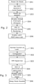
- FIG. 2 shows flow diagram of a start-up operation process when the electronic fuse device shown in Figure 1 is first turned on or reset.
- the microcontroller software is turned on, which then initiates a configuration routine 202 in which the PWM signal output by the timer module 13 is set to provide a suitable current threshold.
- the threshold may be selected according to system design parameters such as attached loads, load types and wiring harness dimensions.
- the microcontroller 8 may then monitor the flowing current, for example, at designated time intervals, using the ADC input 16.
- the latch 7 may also be activated in step 206 in order to keep the load 2 powered, even if the microcontroller 8 is ramped down during sleep mode.
- Figure 3 shows a flow diagram of operating steps of the electronic fuse device during the microcontroller's active mode 301 under normal current conditions.
- the amount of current flowing through path 6 is below the threshold and therefore the comparator 21 does not output the interrupt signal and hence the NMI terminal 12 is not activated (steps 302 and 303).
- the microcontroller 8 monitors the current flowing using the ADC input 16 in intervals, as needed (step 304) and the latch 7 may be activated in step 305 to hold the MOSFET 5 in an ON state.
- the microcontroller's software may also decide to leave the system in this active mode permanently, or transfer itself into a lower powered sleep mode (step 306) .
- FIG. 4 shows a flow diagram of the operational steps of the electronic fuse device 1 in an overcurrent scenario, for instance as a result of a short circuit occurrence.
- the overcurrent event causes the comparator 21 to output an interrupt signal to NMI terminal 12, which activates the NMI routine in step 403 and forces the microcontroller 8 to wake up.
- This also raises a digital flag in the interrupt system of microcontroller 8, invoking an interrupt service routine which prompts the microcontroller 8 to read out the ADC input 16 and determine the nature of the mitigation procedure that should then take place.
- the microcontroller software may rapidly switch off the MOSFET 5.
- the microcontroller 8 may maintain the MOSFET 5 connection to maintain system availability.
- the microcontroller 8 can monitor the load 2 using the current feedback received via the ADC input 16.
- ongoing diagnostic functionality or complex fusing algorithms may be implemented in the microcontroller 8 to, for instance, monitor current characteristics over time. If an overcurrent event arises, the analog components provide for the rapid triggering of a protective response.
- the comparator 21 responds to any increase in current above the threshold and activates the NMI 12, which triggers the microcontroller 8 to rapidly diagnose the fault based on the ADC input 16 and, if appropriate, switch the MOSFET 5 to disconnect the load 2 from the current path 6.
- this trigging action may be initiated even if the microcontroller 8 is in a low-power sleep mode.
- the microcontroller 16 may power down active monitoring the ADC input 16 to conserve power and rely on the analog comparator to initiate an overcurrent response. Not only does this provide for low latency response times, but because the microcontroller 8 subsequently determines the response action, more sophisticated characterisation of the issue can be undertaken. For instance, momentary current spikes may be differentiated from prolonged overcurrent situations to maintain system availability whenever possible. This contrasts with the more simplistic response actions undertaken by conventional smart current drivers, which will often disconnect loads in response to any detected current spike.
- the arrangement therefore allows the flexibility provided by a microcontroller 8 to be implemented, while still providing current overload protection when the microcontroller is sleep mode without substantively adding to the systems quiescent current demands. This is especially important in automotive applications where it is necessary to power down as many non-critical systems as possible when the engine is turned off, but nevertheless certain critical systems have to remain powered.
- a further advantage is that the triggering threshold may be freely adjusted by the microcontroller using the PWM output signal 14, or for example using a Digital to Analog converter.
- the use of a PWM signal is particularly advantageous because the signal can be maintained by an internal timer module 13, without relying on continued CPU execution. This allows a low quiescent current demand to be achieved while generating the threshold signal when the microcontroller is in low power mode.
- segmentation of logical and analog power part not only allows multiple fuses to be monitored by a single microcontroller, but it also allows a single microcontroller to monitor the entire bandwith of different vehicle currents. That is, different analog triggering circuits may be associated with different loads, with their respective thresholds set based on the respective load's characteristics.
- the microcontroller may perform other functions in addition to its role as part of an electronic fuse device.
- the microcontroller may be a vehicle safety microcontroller to which the triggering components are subsequently coupled.
- existing off-the-shelf microcontroller devices may be programmed for use in embodiments.
- embodiments may be provided as a complete electronic fuse device comprising both the digital microcontroller and one or more analog triggering circuits.
Landscapes
- Physics & Mathematics (AREA)
- Nonlinear Science (AREA)
- Emergency Protection Circuit Devices (AREA)
Priority Applications (3)
| Application Number | Priority Date | Filing Date | Title |
|---|---|---|---|
| EP20191585.7A EP3958466B1 (de) | 2020-08-18 | 2020-08-18 | Auslöseschaltung und elektronische sicherung damit |
| CN202110935745.7A CN114079262B (zh) | 2020-08-18 | 2021-08-16 | 触发电路和包括该触发电路的电子保险丝装置 |
| US17/404,763 US11611205B2 (en) | 2020-08-18 | 2021-08-17 | Triggering circuit and electronic fuse device incorporating the same |
Applications Claiming Priority (1)
| Application Number | Priority Date | Filing Date | Title |
|---|---|---|---|
| EP20191585.7A EP3958466B1 (de) | 2020-08-18 | 2020-08-18 | Auslöseschaltung und elektronische sicherung damit |
Publications (2)
| Publication Number | Publication Date |
|---|---|
| EP3958466A1 true EP3958466A1 (de) | 2022-02-23 |
| EP3958466B1 EP3958466B1 (de) | 2024-05-15 |
Family
ID=72147903
Family Applications (1)
| Application Number | Title | Priority Date | Filing Date |
|---|---|---|---|
| EP20191585.7A Active EP3958466B1 (de) | 2020-08-18 | 2020-08-18 | Auslöseschaltung und elektronische sicherung damit |
Country Status (3)
| Country | Link |
|---|---|
| US (1) | US11611205B2 (de) |
| EP (1) | EP3958466B1 (de) |
| CN (1) | CN114079262B (de) |
Families Citing this family (4)
| Publication number | Priority date | Publication date | Assignee | Title |
|---|---|---|---|---|
| GB2598316B (en) * | 2020-08-25 | 2022-11-16 | Ge Aviat Systems Ltd | Control circuit for a power distribution node |
| CN112636597B (zh) * | 2020-12-03 | 2022-03-22 | 成都芯源系统有限公司 | 电源管理电路和集成电路及其过流保护方法 |
| US11557891B2 (en) * | 2020-12-10 | 2023-01-17 | Stmicroelectronics S.R.L. | Overcurrent detection circuit, corresponding system and method |
| CN115882421B (zh) * | 2023-02-23 | 2023-06-23 | 杰华特微电子股份有限公司 | 电子保险丝电路及应用其的电路系统 |
Citations (4)
| Publication number | Priority date | Publication date | Assignee | Title |
|---|---|---|---|---|
| EP1150410A2 (de) * | 2000-04-26 | 2001-10-31 | Eaton Corporation | Festkörper-Schutzschaltung für elektrisches Gerät |
| EP3159992A1 (de) * | 2015-10-20 | 2017-04-26 | Nxp B.V. | Steuerungsvorrichtung für eine elektronische sicherung und verfahren zur steuerung einer elektronischen sicherung |
| US10090751B1 (en) * | 2018-02-21 | 2018-10-02 | Ixys, Llc | Gate driver for switching converter having body diode power loss minimization |
| US20180287365A1 (en) * | 2017-03-30 | 2018-10-04 | Infineon Technologies Ag | Electronic Switch for Electronic Fuse |
Family Cites Families (8)
| Publication number | Priority date | Publication date | Assignee | Title |
|---|---|---|---|---|
| DE19941699A1 (de) * | 1999-09-02 | 2001-03-08 | Bosch Gmbh Robert | Halbleitersicherung für elektrische Verbraucher |
| JP4298256B2 (ja) * | 2002-10-08 | 2009-07-15 | キヤノン株式会社 | 画像形成装置 |
| JP4779342B2 (ja) * | 2004-11-25 | 2011-09-28 | パナソニック電工株式会社 | 無線センサ装置 |
| JP4688693B2 (ja) * | 2006-02-22 | 2011-05-25 | 株式会社オートネットワーク技術研究所 | 電力供給制御装置 |
| JP5351793B2 (ja) * | 2010-02-05 | 2013-11-27 | 矢崎総業株式会社 | 過電流保護装置及び過電流保護システム |
| DE102013216492A1 (de) * | 2013-08-20 | 2015-02-26 | Conti Temic Microelectronic Gmbh | Verfahren zum Schützen eines steuerbaren Halbleiterschalters gegen Überlast und Kurzschluss in einem Lastkreis |
| US9759758B2 (en) * | 2014-04-25 | 2017-09-12 | Leviton Manufacturing Co., Inc. | Ground fault detector |
| US9954548B2 (en) * | 2016-04-08 | 2018-04-24 | Infineon Technologies Ag | Electronic switching and protection circuit with a logarithmic ADC |
-
2020
- 2020-08-18 EP EP20191585.7A patent/EP3958466B1/de active Active
-
2021
- 2021-08-16 CN CN202110935745.7A patent/CN114079262B/zh active Active
- 2021-08-17 US US17/404,763 patent/US11611205B2/en active Active
Patent Citations (4)
| Publication number | Priority date | Publication date | Assignee | Title |
|---|---|---|---|---|
| EP1150410A2 (de) * | 2000-04-26 | 2001-10-31 | Eaton Corporation | Festkörper-Schutzschaltung für elektrisches Gerät |
| EP3159992A1 (de) * | 2015-10-20 | 2017-04-26 | Nxp B.V. | Steuerungsvorrichtung für eine elektronische sicherung und verfahren zur steuerung einer elektronischen sicherung |
| US20180287365A1 (en) * | 2017-03-30 | 2018-10-04 | Infineon Technologies Ag | Electronic Switch for Electronic Fuse |
| US10090751B1 (en) * | 2018-02-21 | 2018-10-02 | Ixys, Llc | Gate driver for switching converter having body diode power loss minimization |
Also Published As
| Publication number | Publication date |
|---|---|
| US11611205B2 (en) | 2023-03-21 |
| EP3958466B1 (de) | 2024-05-15 |
| US20220060011A1 (en) | 2022-02-24 |
| CN114079262A (zh) | 2022-02-22 |
| CN114079262B (zh) | 2024-02-02 |
Similar Documents
| Publication | Publication Date | Title |
|---|---|---|
| EP3958466B1 (de) | Auslöseschaltung und elektronische sicherung damit | |
| US8547676B2 (en) | Overcurrent protection device and overcurrent protection system | |
| KR100197913B1 (ko) | 분리 입력 리셋 신호 레벨을 갖는 모스게이트된 보호 3핀 파워스위치 | |
| US10044180B2 (en) | Electronic circuit breaker for an electrical load in an on-board electrical system of a motor vehicle | |
| US7012393B2 (en) | Motor drive | |
| US11201498B2 (en) | Power supply system | |
| CN109477862B (zh) | 车载控制装置 | |
| JPH0340517A (ja) | パワーデバイスの駆動・保護回路 | |
| US10153632B2 (en) | Device and method for protecting an electrical system component of a vehicle electrical system | |
| EP2127080B1 (de) | Stromversorgungsschaltvorrichtung mit starküberlastungsdetektion | |
| US20190123547A1 (en) | Relay device | |
| JP2594892B2 (ja) | 自動車用電子制御装置及び自動車用電子制御装置を保護する方法 | |
| US11799282B2 (en) | Electrical safety system for providing overcurrent protection of an electrical circuit in a vehicle | |
| CN114290901A (zh) | 电压监控方法、电压监控装置及电动汽车 | |
| CN111404423A (zh) | 安全转矩关断控制方法、电路及电机控制器 | |
| JP3314922B2 (ja) | 負荷駆動システム及びその故障検出方法 | |
| KR20190013648A (ko) | 자가 진단이 가능한 워치독 모니터링 시스템 | |
| US20220271556A1 (en) | Current control for multi-port charging circuit | |
| US7224561B2 (en) | Protective circuit and method for operating said protective circuit, in particular for overvoltage protection for an electronic control system for a motor vehicle | |
| US9809120B2 (en) | Discrete under voltage/over voltage monitoring circuit | |
| JP3572878B2 (ja) | 車両用回路保護装置 | |
| KR101887906B1 (ko) | 전력 소자 모듈의 온도 센싱 장치 | |
| CN111525497B (zh) | 一种缓冲电路及电子设备 | |
| JP2019193344A (ja) | 電力供給装置 | |
| CN113497609A (zh) | 用于配电开关的驱动器 |
Legal Events
| Date | Code | Title | Description |
|---|---|---|---|
| PUAI | Public reference made under article 153(3) epc to a published international application that has entered the european phase |
Free format text: ORIGINAL CODE: 0009012 |
|
| STAA | Information on the status of an ep patent application or granted ep patent |
Free format text: STATUS: THE APPLICATION HAS BEEN PUBLISHED |
|
| AK | Designated contracting states |
Kind code of ref document: A1 Designated state(s): AL AT BE BG CH CY CZ DE DK EE ES FI FR GB GR HR HU IE IS IT LI LT LU LV MC MK MT NL NO PL PT RO RS SE SI SK SM TR |
|
| STAA | Information on the status of an ep patent application or granted ep patent |
Free format text: STATUS: REQUEST FOR EXAMINATION WAS MADE |
|
| 17P | Request for examination filed |
Effective date: 20220805 |
|
| RBV | Designated contracting states (corrected) |
Designated state(s): AL AT BE BG CH CY CZ DE DK EE ES FI FR GB GR HR HU IE IS IT LI LT LU LV MC MK MT NL NO PL PT RO RS SE SI SK SM TR |
|
| RAP3 | Party data changed (applicant data changed or rights of an application transferred) |
Owner name: APTIV TECHNOLOGIES LIMITED |
|
| GRAP | Despatch of communication of intention to grant a patent |
Free format text: ORIGINAL CODE: EPIDOSNIGR1 |
|
| STAA | Information on the status of an ep patent application or granted ep patent |
Free format text: STATUS: GRANT OF PATENT IS INTENDED |
|
| INTG | Intention to grant announced |
Effective date: 20240216 |
|
| GRAS | Grant fee paid |
Free format text: ORIGINAL CODE: EPIDOSNIGR3 |
|
| GRAA | (expected) grant |
Free format text: ORIGINAL CODE: 0009210 |
|
| STAA | Information on the status of an ep patent application or granted ep patent |
Free format text: STATUS: THE PATENT HAS BEEN GRANTED |
|
| RAP1 | Party data changed (applicant data changed or rights of an application transferred) |
Owner name: APTIV TECHNOLOGIES AG |
|
| AK | Designated contracting states |
Kind code of ref document: B1 Designated state(s): AL AT BE BG CH CY CZ DE DK EE ES FI FR GB GR HR HU IE IS IT LI LT LU LV MC MK MT NL NO PL PT RO RS SE SI SK SM TR |
|
| P01 | Opt-out of the competence of the unified patent court (upc) registered |
Effective date: 20240408 |
|
| REG | Reference to a national code |
Ref country code: CH Ref legal event code: EP |
|
| REG | Reference to a national code |
Ref country code: DE Ref legal event code: R096 Ref document number: 602020030847 Country of ref document: DE |
|
| REG | Reference to a national code |
Ref country code: IE Ref legal event code: FG4D |
|
| REG | Reference to a national code |
Ref country code: LT Ref legal event code: MG9D |