EP3944288A1 - Semiconductor wafer and method of manufacturing semiconductor device - Google Patents
Semiconductor wafer and method of manufacturing semiconductor device Download PDFInfo
- Publication number
- EP3944288A1 EP3944288A1 EP20773287.6A EP20773287A EP3944288A1 EP 3944288 A1 EP3944288 A1 EP 3944288A1 EP 20773287 A EP20773287 A EP 20773287A EP 3944288 A1 EP3944288 A1 EP 3944288A1
- Authority
- EP
- European Patent Office
- Prior art keywords
- semiconductor wafer
- recess
- wafer
- film
- semiconductor
- Prior art date
- Legal status (The legal status is an assumption and is not a legal conclusion. Google has not performed a legal analysis and makes no representation as to the accuracy of the status listed.)
- Pending
Links
Images







Classifications
-
- H—ELECTRICITY
- H10—SEMICONDUCTOR DEVICES; ELECTRIC SOLID-STATE DEVICES NOT OTHERWISE PROVIDED FOR
- H10P—GENERIC PROCESSES OR APPARATUS FOR THE MANUFACTURE OR TREATMENT OF DEVICES COVERED BY CLASS H10
- H10P50/00—Etching of wafers, substrates or parts of devices
-
- H—ELECTRICITY
- H10—SEMICONDUCTOR DEVICES; ELECTRIC SOLID-STATE DEVICES NOT OTHERWISE PROVIDED FOR
- H10P—GENERIC PROCESSES OR APPARATUS FOR THE MANUFACTURE OR TREATMENT OF DEVICES COVERED BY CLASS H10
- H10P74/00—Testing or measuring during manufacture or treatment of wafers, substrates or devices
- H10P74/27—Structural arrangements therefor
-
- C—CHEMISTRY; METALLURGY
- C30—CRYSTAL GROWTH
- C30B—SINGLE-CRYSTAL GROWTH; UNIDIRECTIONAL SOLIDIFICATION OF EUTECTIC MATERIAL OR UNIDIRECTIONAL DEMIXING OF EUTECTOID MATERIAL; REFINING BY ZONE-MELTING OF MATERIAL; PRODUCTION OF A HOMOGENEOUS POLYCRYSTALLINE MATERIAL WITH DEFINED STRUCTURE; SINGLE CRYSTALS OR HOMOGENEOUS POLYCRYSTALLINE MATERIAL WITH DEFINED STRUCTURE; AFTER-TREATMENT OF SINGLE CRYSTALS OR A HOMOGENEOUS POLYCRYSTALLINE MATERIAL WITH DEFINED STRUCTURE; APPARATUS THEREFOR
- C30B25/00—Single-crystal growth by chemical reaction of reactive gases, e.g. chemical vapour-deposition growth
- C30B25/02—Epitaxial-layer growth
- C30B25/18—Epitaxial-layer growth characterised by the substrate
- C30B25/186—Epitaxial-layer growth characterised by the substrate being specially pre-treated by, e.g. chemical or physical means
-
- C—CHEMISTRY; METALLURGY
- C30—CRYSTAL GROWTH
- C30B—SINGLE-CRYSTAL GROWTH; UNIDIRECTIONAL SOLIDIFICATION OF EUTECTIC MATERIAL OR UNIDIRECTIONAL DEMIXING OF EUTECTOID MATERIAL; REFINING BY ZONE-MELTING OF MATERIAL; PRODUCTION OF A HOMOGENEOUS POLYCRYSTALLINE MATERIAL WITH DEFINED STRUCTURE; SINGLE CRYSTALS OR HOMOGENEOUS POLYCRYSTALLINE MATERIAL WITH DEFINED STRUCTURE; AFTER-TREATMENT OF SINGLE CRYSTALS OR A HOMOGENEOUS POLYCRYSTALLINE MATERIAL WITH DEFINED STRUCTURE; APPARATUS THEREFOR
- C30B29/00—Single crystals or homogeneous polycrystalline material with defined structure characterised by the material or by their shape
- C30B29/02—Elements
- C30B29/06—Silicon
-
- C—CHEMISTRY; METALLURGY
- C30—CRYSTAL GROWTH
- C30B—SINGLE-CRYSTAL GROWTH; UNIDIRECTIONAL SOLIDIFICATION OF EUTECTIC MATERIAL OR UNIDIRECTIONAL DEMIXING OF EUTECTOID MATERIAL; REFINING BY ZONE-MELTING OF MATERIAL; PRODUCTION OF A HOMOGENEOUS POLYCRYSTALLINE MATERIAL WITH DEFINED STRUCTURE; SINGLE CRYSTALS OR HOMOGENEOUS POLYCRYSTALLINE MATERIAL WITH DEFINED STRUCTURE; AFTER-TREATMENT OF SINGLE CRYSTALS OR A HOMOGENEOUS POLYCRYSTALLINE MATERIAL WITH DEFINED STRUCTURE; APPARATUS THEREFOR
- C30B29/00—Single crystals or homogeneous polycrystalline material with defined structure characterised by the material or by their shape
- C30B29/10—Inorganic compounds or compositions
- C30B29/16—Oxides
- C30B29/20—Aluminium oxides
-
- C—CHEMISTRY; METALLURGY
- C30—CRYSTAL GROWTH
- C30B—SINGLE-CRYSTAL GROWTH; UNIDIRECTIONAL SOLIDIFICATION OF EUTECTIC MATERIAL OR UNIDIRECTIONAL DEMIXING OF EUTECTOID MATERIAL; REFINING BY ZONE-MELTING OF MATERIAL; PRODUCTION OF A HOMOGENEOUS POLYCRYSTALLINE MATERIAL WITH DEFINED STRUCTURE; SINGLE CRYSTALS OR HOMOGENEOUS POLYCRYSTALLINE MATERIAL WITH DEFINED STRUCTURE; AFTER-TREATMENT OF SINGLE CRYSTALS OR A HOMOGENEOUS POLYCRYSTALLINE MATERIAL WITH DEFINED STRUCTURE; APPARATUS THEREFOR
- C30B29/00—Single crystals or homogeneous polycrystalline material with defined structure characterised by the material or by their shape
- C30B29/10—Inorganic compounds or compositions
- C30B29/36—Carbides
-
- H—ELECTRICITY
- H10—SEMICONDUCTOR DEVICES; ELECTRIC SOLID-STATE DEVICES NOT OTHERWISE PROVIDED FOR
- H10B—ELECTRONIC MEMORY DEVICES
- H10B43/00—EEPROM devices comprising charge-trapping gate insulators
- H10B43/20—EEPROM devices comprising charge-trapping gate insulators characterised by three-dimensional [3D] arrangements, e.g. with cells on different height levels
- H10B43/23—EEPROM devices comprising charge-trapping gate insulators characterised by three-dimensional [3D] arrangements, e.g. with cells on different height levels with source and drain on different levels, e.g. with sloping channels
- H10B43/27—EEPROM devices comprising charge-trapping gate insulators characterised by three-dimensional [3D] arrangements, e.g. with cells on different height levels with source and drain on different levels, e.g. with sloping channels the channels comprising vertical portions, e.g. U-shaped channels
-
- H—ELECTRICITY
- H10—SEMICONDUCTOR DEVICES; ELECTRIC SOLID-STATE DEVICES NOT OTHERWISE PROVIDED FOR
- H10D—INORGANIC ELECTRIC SEMICONDUCTOR DEVICES
- H10D30/00—Field-effect transistors [FET]
- H10D30/60—Insulated-gate field-effect transistors [IGFET]
- H10D30/69—IGFETs having charge trapping gate insulators, e.g. MNOS transistors
-
- H—ELECTRICITY
- H10—SEMICONDUCTOR DEVICES; ELECTRIC SOLID-STATE DEVICES NOT OTHERWISE PROVIDED FOR
- H10P—GENERIC PROCESSES OR APPARATUS FOR THE MANUFACTURE OR TREATMENT OF DEVICES COVERED BY CLASS H10
- H10P74/00—Testing or measuring during manufacture or treatment of wafers, substrates or devices
- H10P74/27—Structural arrangements therefor
- H10P74/277—Circuits for electrically characterising or monitoring manufacturing processes, e.g. circuits in tested chips or circuits in testing wafers
-
- H—ELECTRICITY
- H10—SEMICONDUCTOR DEVICES; ELECTRIC SOLID-STATE DEVICES NOT OTHERWISE PROVIDED FOR
- H10P—GENERIC PROCESSES OR APPARATUS FOR THE MANUFACTURE OR TREATMENT OF DEVICES COVERED BY CLASS H10
- H10P90/00—Preparation of wafers not covered by a single main group of this subclass, e.g. wafer reinforcement
-
- H—ELECTRICITY
- H10—SEMICONDUCTOR DEVICES; ELECTRIC SOLID-STATE DEVICES NOT OTHERWISE PROVIDED FOR
- H10P—GENERIC PROCESSES OR APPARATUS FOR THE MANUFACTURE OR TREATMENT OF DEVICES COVERED BY CLASS H10
- H10P90/00—Preparation of wafers not covered by a single main group of this subclass, e.g. wafer reinforcement
- H10P90/12—Preparing bulk and homogeneous wafers
-
- H—ELECTRICITY
- H10—SEMICONDUCTOR DEVICES; ELECTRIC SOLID-STATE DEVICES NOT OTHERWISE PROVIDED FOR
- H10P—GENERIC PROCESSES OR APPARATUS FOR THE MANUFACTURE OR TREATMENT OF DEVICES COVERED BY CLASS H10
- H10P50/00—Etching of wafers, substrates or parts of devices
- H10P50/60—Wet etching
- H10P50/64—Wet etching of semiconductor materials
- H10P50/642—Chemical etching
-
- H—ELECTRICITY
- H10—SEMICONDUCTOR DEVICES; ELECTRIC SOLID-STATE DEVICES NOT OTHERWISE PROVIDED FOR
- H10P—GENERIC PROCESSES OR APPARATUS FOR THE MANUFACTURE OR TREATMENT OF DEVICES COVERED BY CLASS H10
- H10P50/00—Etching of wafers, substrates or parts of devices
- H10P50/60—Wet etching
- H10P50/64—Wet etching of semiconductor materials
- H10P50/642—Chemical etching
- H10P50/644—Anisotropic liquid etching
-
- H—ELECTRICITY
- H10—SEMICONDUCTOR DEVICES; ELECTRIC SOLID-STATE DEVICES NOT OTHERWISE PROVIDED FOR
- H10P—GENERIC PROCESSES OR APPARATUS FOR THE MANUFACTURE OR TREATMENT OF DEVICES COVERED BY CLASS H10
- H10P72/00—Handling or holding of wafers, substrates or devices during manufacture or treatment thereof
- H10P72/04—Apparatus for manufacture or treatment
- H10P72/0431—Apparatus for thermal treatment
- H10P72/0432—Apparatus for thermal treatment mainly by conduction
-
- H—ELECTRICITY
- H10—SEMICONDUCTOR DEVICES; ELECTRIC SOLID-STATE DEVICES NOT OTHERWISE PROVIDED FOR
- H10P—GENERIC PROCESSES OR APPARATUS FOR THE MANUFACTURE OR TREATMENT OF DEVICES COVERED BY CLASS H10
- H10P74/00—Testing or measuring during manufacture or treatment of wafers, substrates or devices
- H10P74/20—Testing or measuring during manufacture or treatment of wafers, substrates or devices characterised by the properties tested or measured, e.g. structural or electrical properties
- H10P74/203—Structural properties, e.g. testing or measuring thicknesses, line widths, warpage, bond strengths or physical defects
Definitions
- Embodiments relate to a semiconductor wafer and a method of manufacturing a semiconductor apparatus.
- the manufacture of a semiconductor device may use Non Product Wafer (NPW) with no semiconductor device formed thereon.
- NPW Non Product Wafer
- known examples of a semiconductor device include memory cells three-dimensionally arranged on a semiconductor wafer.
- the semiconductor wafer of the embodiment includes a surface having at least one recess including an inner wall surface. The inner wall surface of the recess is exposed.
- Fig. 1 is a schematic view of an external appearance of a semiconductor wafer
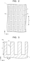
- Fig. 2 is a schematic upper view illustrating a structural example of the semiconductor wafer, illustrating a part of an X-Y plane including an X-axis of the semiconductor wafer and a Y-axis perpendicular to the X-axis
- Fig. 3 is a schematic sectional view illustrating the structural example of the semiconductor wafer, illustrating a part of an X-Z section including the X-axis and a Z-axis perpendicular to the X-axis and the Y-axis.
- a semiconductor wafer 1 is an NPW, and is used for previously evaluating and measuring film formation, etching, and other various processes in semiconductor manufacture.
- the semiconductor wafer 1 is used for evaluating and measuring a film formation process such as chemical vapor deposition (CVD) in which a source gas is made to react with a wafer surface to form a thin film or atomic layer deposition (ALD), and an etching process such as chemical dry etching (CDE) in which plasma is supplied to a wafer surface to perform etching on a thin film, atomic layer etching (ALE) in which a source gas is supplied to a surface to perform etching on a thin film, or wet etching in which liquid is supplied.
- CVD chemical vapor deposition
- ALD atomic layer deposition
- ALE atomic layer etching
- the semiconductor wafer 1 is also used for reproducibility tests for the processes, and the like.
- the semiconductor wafer 1 may be processed in the chamber together with a wafer having a semiconductor device formed thereon.
- the semiconductor wafer 1 in the embodiment can also be referred to as a dummy wafer, a test piece, or the like.
- the semiconductor wafer 1 includes a surface 10a extending in an X-axis direction and a Y-axis direction, and a surface 10b being a surface opposite to the surface 10a.
- a surface area of the surface 10a is preferably about the same as a surface area of a device formation surface of a semiconductor wafer with a semiconductor device formed thereon or in the middle of the formation of a semiconductor device.
- Examples of the semiconductor wafer 1 include a silicon wafer, a silicon carbide wafer, a glass wafer, a quartz wafer, a sapphire wafer, a compound semiconductor wafer such as a GaAs substrate, and the like.
- a shape of the semiconductor wafer 1 is not limited to the shape illustrated in Fig. 1 , and it may be, for example, a shape having an orientation flat.
- the surface 10a has a pattern including at least one recess 11.
- the recess 11 includes an inner wall surface 11a.
- the inner wall surface 11a is exposed to the surface 10a.
- the plurality of recesses 11 are juxtaposed along the X-axis direction of the surface 10a as illustrated in Fig. 2 , and are extended in a line form along the Y-axis direction of the surface 10a.
- a length L of the recess 11 in a long-side direction is, for example, 4 ⁇ m or more and is preferably 40 ⁇ m or more.
- An interval between the recesses 11 adjacent along the X-axis direction is, for example, 0.4 ⁇ m or more and 14 ⁇ m or less and is preferably 1 ⁇ m or less. End portions of the recesses 11 adjacent along the X-axis direction may be displaced from each other along the Y-axis direction.
- An aspect ratio of the recess 11 is, for example, 50 or more and 1750 or less.
- the aspect ratio is defined by a ratio of a depth D of the recess 11 to a width W of the recess 11 illustrated in Fig. 3 .
- the width W of the recess 11 is, for example, 0.4 ⁇ m or more and 14 ⁇ m or less.
- the depth D of the recess 11 is, for example, 20 ⁇ m or more and a thickness of the semiconductor wafer 1 or less, and the recess 11 may penetrate the semiconductor wafer 1.
- a surface area of the surface 10a is, for example, 50 times or more and preferably 100 times or more a surface area in a case where the recess 11 is not formed. In other words, when the recess or the like is not formed in the surface 10b, the surface area of the surface 10a is 50 times or more and preferably 100 times or more a surface area of the surface 10b.
- Examples of the recess 11 preferably has a depth D from the surface 10a of 20 ⁇ m or more and an aspect ratio of 50 or more. This increases the surface area of the surface 10a, and to form the recess 11 with which a film to be formed on the surface 10a is easily removed.
- the recess 11 may also be formed via a partition 12.
- the partition 12 functions as a beam and thereby enables to support the recess 11, thus prevent the deformation of the recess 11.
- the partition 12 is preferably provided, for example, at intervals of 100 ⁇ m or more in the Y-axis direction. Further, lengths of a plurality of partitions 12 in the Y-axis direction are preferably the same. Positions of the partitions 12 between the recesses 11 adjacent in the X-axis direction may be displaced from each other along the Y-axis direction and regions between the adjacent recesses 11 are connected via the partition 12 as illustrated in Fig. 2 .
- the recess 11 may also include a plurality of recesses which extend along mutually different directions.
- Fig. 4 is a schematic upper view illustrating a structural example of the semiconductor wafer 1, illustrating a part of the X-Y plane.
- the surface 10a of the semiconductor wafer 1 illustrated in Fig. 4 includes a region 101 and a region 102.
- the region 101 and the region 102 are alternately arranged, for example, along the X-axis direction and the Y-axis direction.
- An interval between the region 101 and the region 102 is, for example, 2 ⁇ m or more.
- Fig. 4 illustrates one shot region of a plurality of shot regions formed on the surface 10a.
- Fig. 5 is a schematic upper view illustrating an intermediate region between the region 101 and the region 102.
- the region 101 has a recess 111
- the region 102 has a recess 112.
- a plurality of recesses 111 are juxtaposed along the X-axis direction, and extended along the Y-axis direction.
- a plurality of plural recesses 112 are juxtaposed along the Y-axis direction, and extended along the X-axis direction.
- the extending direction (the length L direction) of the recess 111 and the extending direction (the length L direction) of the recess 112 are not limited to directions perpendicular to each other, but only have to be directions intersecting with each other.
- the recess 111 and the recess 112 are included in the recess 11. Therefore, for the other explanation of the recess 111 and the recess 112, the explanation of the recess 11 can be appropriately cited.
- the structure of the surface 10a explained above may also be formed on the surface 10b.
- the semiconductor wafer 1 can be used as a test piece on which a film is formed and evaluation is performed thereon.
- the semiconductor wafer 1 can also be used as a test piece on which a film is formed, etching is then performed, and evaluation is performed thereon.
- the semiconductor wafer 1 is likely to warp since it has a pair of surfaces with different surface areas and a large difference in amount of film formation on the pair of surfaces. Accordingly, if all of the plurality of recesses 11 extend in the same direction, a stress is applied in one direction, resulting in that the warpage of the semiconductor wafer 1 is likely to be increased. In contrast to this, the plurality of recesses 11 extending in the plurality of directions can disperse the directions in which the stress is applied, resulting in prevention of the warpage of the semiconductor wafer 1.
- the semiconductor wafer 1 can be repeatedly used as the test piece. Specifically, it is also possible to continuously perform film formation steps on the semiconductor wafer 1, or continuously perform a film formation step and an etching step on the semiconductor wafer 1.
- the recess 11 increases the surface area to prevent the change in surface area even when the films are continuously formed, resulting in easily removing the film even when the etching.
- the surface 10a may further have a region 103 as illustrated in Fig. 4 .
- the region 103 is preferably a flat surface having no recess 11.
- the presence of the flat surface in the region 103 enables to measure a thickness, a density, and a composition of a film to be formed on the surface 10a with a measuring device such as a spectral ellipsometer, an X-ray photoelectron spectroscopy (XPS), a fluorescent X-ray analysis, or a Fourier transform infrared spectrophotometer (FTIR), each measuring device having a minimum measurement region larger than a flat part between the recesses 11.
- An area of the region 103 may be smaller than, for example, an area of the region 101 or an area of the region 102.
- the region 103 is formed, for example, for each of the plurality of shot regions of the surface 10a.
- the strong recess 11 can be formed by controlling the shape of the recess for increasing the surface area of the semiconductor wafer 1. This recess prevents the change in surface area after repeatedly using the semiconductor wafer 1. This recess leads to provide a semiconductor wafer having a larger surface area.
- the dimension of the recess 11 explained above is preferably set according to the kind and the thickness of the film to be formed.
- Examples of the semiconductor wafer 1 can be manufactured using metal-assisted chemical etching (MACE).
- MACE metal-assisted chemical etching
- the MACE is a technique of immersing a substrate having a catalyst layer formed on a surface thereof in a chemical solution to thereby almost vertically etch only a region in contact with the catalyst layer.
- Fig. 6 to Fig. 8 are views for explaining a method example of manufacturing a semiconductor wafer.
- the method example of manufacturing the semiconductor wafer includes a catalyst layer formation step, an etching step, and a catalyst layer removal step.
- a catalyst layer 2 is formed on the surface 10a of the semiconductor wafer 1 as illustrated in Fig. 6 .
- the catalyst layer 2 contains a catalyst of noble metal such as, for example, gold, silver, platinum, iridium, or palladium.
- the catalyst layer 2 can be formed by using, for example, sputtering, a CVD method, a plating method, or the like.
- the catalyst layer 2 may contain a catalyst of a carbon material such as graphene.
- the semiconductor wafer 1 is immersed in a first chemical solution (etching solution) as illustrated in Fig. 7 .
- first chemical solution include a mixed solution of hydrofluoric acid and a hydrogen peroxide solution.
- the semiconductor wafer 1 When the semiconductor wafer 1 is immersed in the first chemical solution, a material such as silicon of the surface 10a is dissolved in the etching solution, at a contact portion between the surface 10a and the catalyst layer 2. When this reaction repeatedly occurs, the semiconductor wafer 1 is almost vertically etched. Thereby, the recess 11 can be formed.
- the shape of the recess 11 is controlled by adjusting, for example, the size of the catalyst layer 2, the etching time, or the like.
- the catalyst layer 2 is removed from the surface 10a as illustrated in Fig. 8 .
- the catalyst layer 2 is removed, for example, by impregnating the semiconductor wafer 1 with a second chemical solution.
- a second chemical solution for example, a mixed solution (aqua regia) of hydrochloric acid and nitric acid can be used.
- the use of the MACE in the manufacture of the semiconductor wafer 1, enables to easily form the recess 11 even when the recess 11 having a large length L, a large depth D, and a large aspect ratio.
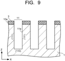
- Fig. 9 is a view for explaining another method example of manufacturing the semiconductor wafer 1. This example includes forming the surface 10a along the (110) plane of the semiconductor wafer 1, forming a mask layer 3 on the surface 10a, and etching the semiconductor wafer 1 along the (111) plane of the semiconductor wafer 1 to form the recess 11.
- the (111) plane of the semiconductor wafer 1 such as a silicon wafer is more stable than the (110) plane. Therefore, the semiconductor wafer 1 can be almost vertically etched along the (111) plane by alkaline etching using, for example, an alkaline chemical solution. This enables to easily form the recess 11 even though the recess 11 has large length L, depth D, and aspect ratio.
- Fig. 10 to Fig. 14 are schematic sectional views illustrating another structural example of the semiconductor wafer 1.
- the above explanation can be appropriately cited.
- the surface 10a of the semiconductor wafer 1 illustrated in Fig. 10 further has a protrusion 13 formed at a bottom portion of the recess 11.
- the protrusion 13 is provided in the recess 11 and extends in the Z-axis direction, for example, from the bottom surface of the recess 11.
- the protrusion 13 is, for example, needle-shaped.
- the protrusion 13 is formed, for example, by forming a through hole along the Z-axis direction in the catalyst layer 2 and then etching the semiconductor wafer 1.
- the formation of the through hole in the catalyst layer 2 facilitates etching of a region facing an opening of a contact portion between the surface 10a and the catalyst layer 2.
- a region not facing the surface 10a and the opening is unlikely to be etched and therefore remains to form the needle-shaped protrusion 13.
- the formation of the protrusion 13 can further increase the surface area of the surface 10a.
- the surface 10a of the semiconductor wafer 1 illustrated in Fig. 11 further has a porous region 14.
- the porous region 14 is formed, for example, by etching an intermediate region between adjacent recesses 11 in the semiconductor wafer 1 with a first chemical solution or a second chemical solution. The formation of the porous region 14 can further increase the surface area of the surface 10a.
- a vacancy 14a in the porous region 14 may be closed by filling the vacancy in the porous region 14 with a filler 4a.
- a protective film 4b may be formed over the entire surface 10a including the porous region 14 as illustrated in Fig. 13 .
- the semiconductor wafer 1 is repeatedly used and thereby can prevent further etching of the porous region 14.
- the filler 4a and the protective film 4b for example, a material having heat resistance and chemical resistance such as carbon, silicon, silicon nitride, or silicon oxide, and silicon carbide or silicon carbonitride is more preferable.
- the vacancy 14a in the porous region 14 may be closed by dissolving the porous region 14 by annealing under a hydrogen atmosphere.
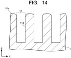
- the surface 10a after the dissolution has a curved surface as illustrated in Fig. 14 .
- the dissolution of the porous region 14 can prevent the porous region 14 from being etched.
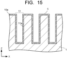
- Fig. 15 is a schematic sectional view illustrating a structural example of a semiconductor apparatus using the semiconductor wafer 1.
- the semiconductor apparatus illustrated in Fig. 15 includes a film 5 provided on the semiconductor wafer 1.
- the film 5 is formed on the surface 10a, for example, using a film-forming apparatus such as a CVD apparatus or the like.
- the film 5 functions, for example, as a base film for evaluating the film formation, such as an etching object film to be etched.
- the thickness of the film 5 is set according to the usage.
- the film 5 may be a stacked film and may be formed on the protective film 4b illustrated in Fig. 13 .
- Fig. 16 is a schematic view illustrating a configuration example of a semiconductor manufacturing apparatus.
- Fig. 16 illustrates a configuration example of LP-CVD (Low Pressure Chemical Vapor Deposition) apparatus.
- a semiconductor manufacturing apparatus 20 illustrated in Fig. 16 includes a chamber 21, and a pipe 23 for supplying a source gas 22 into the chamber 21.
- the semiconductor manufacturing apparatus 20 further includes a vacuum pump, a heater, an exhaust system, a power source, a control circuit, and so on which are not illustrated.
- the semiconductor wafer 1 as a dummy wafer may be conveyed together with a device wafer 9 into the same chamber 21 to be simultaneously processed with the device wafer 9, the device wafer 9 being a semiconductor wafer with a semiconductor device formed thereon or in the middle of the formation of a semiconductor device.
- a method example of manufacturing the semiconductor apparatus in this case includes placing the device wafer 9 into the chamber 21, placing the semiconductor wafer 1 of the embodiment into the chamber 21, and simultaneously processing the device wafer 9 and the semiconductor wafer 1 in the chamber 21.
- the device wafer 9 and the semiconductor wafer 1 are placed into the chamber 21 at the same step or different steps.
- Fig. 16 illustrates an example in which, when a plurality of device wafers 9 are processed in the chamber 21, at least one semiconductor wafer 1 is placed together with the plurality of device wafers 9 in the chamber 21, and the wafers are simultaneously subjected to film formation processing. Although at least one or more semiconductor wafers 1 only have to be placed, it is preferable to place a plurality of the semiconductor wafers 1 as illustrated in Fig. 16 . Further, the semiconductor wafer 1 is preferably arranged in at least an upper region or a lower region in the chamber 21 as illustrated in Fig. 16 .
- a semiconductor device to be formed on the device wafer 9 is, for example, a three-dimensional NAND-type flash memory.
- a film formation step in a method of manufacturing the three-dimensional NAND-type flash memory will be explained.
- Fig. 17 is a schematic view illustrating a structural example of a semiconductor device.
- the semiconductor device illustrated in Fig. 17 includes a core insulating film 91, a semiconductor channel layer 92, a memory film 93 including a tunnel insulating film 931, a charge storage layer 932, and a block insulating film 933, an electrode material layer 94, a metal layer 95, and an insulation layer 96.
- the electrode material layer 94 functions as a gate electrode (word line).
- the core insulator 91, the semiconductor channel layer 92, and the memory film 93 are formed in a memory hole H, and constitute a memory cell.
- the block insulating film 933 is, for example, a SiO 2 film (silicon oxide film).
- the charge storage layer 932 is, for example, a SiN film (silicon nitride film).
- the tunnel insulating film 931 is a stacked film including, for example, a SiO 2 film and a SiON film (silicon oxynitride film).
- the semiconductor channel layer 92 is, for example, a polysilicon layer.
- the core insulator 91 is, for example, a SiO 2 film.
- the electrode material layer 94, the metal layer 95, and the insulation layer 96 are, for example, a W layer (tungsten layer), a TiN film (titanium nitride film), and an Al 2 O 3 film (aluminum oxide film), respectively.
- the metal layer 95 functions as a barrier metal layer in the above-explained electrode layer
- the insulation layer 96 functions as a block insulating film together with the above-explained block insulating film 933.
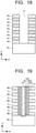
- a method example of manufacturing the semiconductor device illustrated in Fig. 17 will be explained using Fig. 18 and Fig. 19 .
- a stacked film in which a plurality of sacrificial layers 97 and a plurality of insulation layers 98 are alternately stacked is formed on a semiconductor wafer 90 such as a silicon wafer, and a memory hole H being a recess is provided in these sacrificial layers 97 and insulation layers 98.
- the sacrificial layer 97 is a region where the electrode material layer is to be formed later.
- the memory hole H is a region where the memory film 93 is to be formed later.
- the semiconductor wafer 1 is used for the formation of the memory film 93, the semiconductor channel layer 92, and the core insulator 91, or the formation of the electrode material layer 94, the metal layer 95, and the insulation layer 96, and for the modification treatment and etching process of those thin films including the sacrificial layers 97 and the insulation layers 98 constituting a side surface of the memory hole H, for example, in manufacturing the semiconductor device.
- the formation of the memory film 93 is performed by conveying, into the chamber 21, the device wafer 9 in a state where the memory hole H is formed in the stack in which the plurality of sacrificial layers 97 and the plurality of insulation layers 98 are alternately stacked illustrated in Fig. 18 and forming the block insulating film 933, the charge storage layer 932, and the tunnel insulating film 931 in this order in the memory hole H.
- the formation of the metal layer 95 and the insulation layer 96 is performed after the formation of the memory film 93, by conveying, into the chamber 21, the device wafer 9 from which the plurality of sacrificial layers have been removed and which thus has cavities C between the plurality of insulation layers 98 and forming the insulation layer 96 and the metal layer 95 in this order in the cavity C as illustrated in Fig. 19 (this is called a replacement step).
- the modification treatment includes oxidation caused by performing treatment using gas containing oxygen, nitridation caused by performing gas phase treatment using nitrogen-containing gas such as ammonia, and crystallization caused by performing heat treatment after or in the middle of the formation of respective layers or films in the formation step of, for example, the sacrificial layers 97 and the insulation layers 98, the block insulating film 933, the charge storage layer 932, the tunnel insulating film, and the semiconductor channel layer 92 in Fig. 18 and Fig. 19 .
- the modification treatment includes treatment of forming a sacrificial layer containing a desired impurity such as boron, phosphorus, or metal after the formation of the layer or film, diffusing the impurity in a targeted layer or film by performing heat treatment, and then etching the sacrificial layer to remove it. This also applies to the electrode material layer 94, the metal layer 95, and the insulation layer 96.
- a desired impurity such as boron, phosphorus, or metal
- the etching process includes a process of reducing a thickness of the layer or film, for example, for each of the sacrificial layers 97 and the insulation layers 98 in Fig. 18 , and the formed block insulating film 933, charge storage layer 932, tunnel insulating film, and semiconductor channel layer 92 in Fig. 19 after the formation of the layer or film, by using an etching gas containing halogen such as fluorine, chlorine, or bromine, or the like.
- an etching gas containing halogen such as fluorine, chlorine, or bromine, or the like.
- the same also applies to the electrode material layer 94, the metal layer 95, and the insulation layer 96.
- At least one semiconductor wafer 1 is conveyed together with the plurality of device wafers 9 into the chamber 21, and subjected to the similar processing. Consequently, when a desired processing result cannot be obtained at a specific position in the chamber 21, the semiconductor wafer 1 can be used as a dummy wafer. Plural processing may be performed.
- the semiconductor wafer 1 is formed with the plurality of recesses 11 so as to increase its surface area. Accordingly, the semiconductor wafer 1 forms dummy wafer having about the same surface area as that of the device wafer 9. Therefore, it is possible to further reduce a variation in film formation in the chamber 21 caused, for example, by a surface area difference, resulting in that uniformity of the film thickness, the film composition, the film density, and so on between the device wafers 9 or within a plane of the device wafer 9 can be further improved. Specifically, it becomes possible to manufacture a semiconductor device with further improved reliability.
- the semiconductor wafer 1 can also be applied to another semiconductor manufacturing apparatus.
- the semiconductor device is not limited to the three-dimensional NAND-type flash memory, and it is also possible to apply another semiconductor device.
Landscapes
- Chemical & Material Sciences (AREA)
- Engineering & Computer Science (AREA)
- Crystallography & Structural Chemistry (AREA)
- Materials Engineering (AREA)
- Metallurgy (AREA)
- Organic Chemistry (AREA)
- Inorganic Chemistry (AREA)
- Chemical Kinetics & Catalysis (AREA)
- General Chemical & Material Sciences (AREA)
- Weting (AREA)
- Non-Volatile Memory (AREA)
- Semiconductor Memories (AREA)
- Manufacturing & Machinery (AREA)
- Chemical Vapour Deposition (AREA)
- Mechanical Treatment Of Semiconductor (AREA)
- Crystals, And After-Treatments Of Crystals (AREA)
- Drying Of Semiconductors (AREA)
- Automation & Control Theory (AREA)
- Container, Conveyance, Adherence, Positioning, Of Wafer (AREA)
- Recrystallisation Techniques (AREA)
- Element Separation (AREA)
Abstract
Description
- Embodiments relate to a semiconductor wafer and a method of manufacturing a semiconductor apparatus.
- The manufacture of a semiconductor device may use Non Product Wafer (NPW) with no semiconductor device formed thereon. Further, known examples of a semiconductor device include memory cells three-dimensionally arranged on a semiconductor wafer.
-
- Reference 1:
WO 2015/012874 - Reference 2:
WO 2010/114887 - A problem to be solved by the inventions of the embodiments is to provide a semiconductor wafer having a larger surface area
- The semiconductor wafer of the embodiment includes a surface having at least one recess including an inner wall surface. The inner wall surface of the recess is exposed.
-
-
Fig. 1 is a schematic view of an external appearance of a semiconductor wafer. -
Fig. 2 is a schematic upper view illustrating a structural example of the semiconductor wafer. -
Fig. 3 is a schematic sectional view illustrating the structural example of the semiconductor wafer. -
Fig. 4 is a schematic upper view illustrating a structural example of a semiconductor wafer. -
Fig. 5 is a schematic upper view illustrating an intermediate region between aregion 101 and aregion 102. -
Fig. 6 is a schematic view for explaining a method example of manufacturing a semiconductor wafer. -
Fig. 7 is a schematic view for explaining the method example of manufacturing the semiconductor wafer. -
Fig. 8 is a schematic view for explaining the method example of manufacturing the semiconductor wafer. -
Fig. 9 is a schematic view for explaining another method example of manufacturing the semiconductor wafer. -
Fig. 10 is a schematic sectional view illustrating another structural example of the semiconductor wafer. -
Fig. 11 is a schematic sectional view illustrating another structural example of the semiconductor wafer. -
Fig. 12 is a schematic sectional view illustrating another structural example of the semiconductor wafer. -
Fig. 13 is a schematic sectional view illustrating another structural example of the semiconductor wafer. -
Fig. 14 is a schematic sectional view illustrating another structural example of the semiconductor wafer. -
Fig. 15 is a schematic sectional view illustrating a structural example of a semiconductor apparatus. -
Fig. 16 is a schematic view illustrating a configuration example of a semiconductor manufacturing apparatus. -
Fig. 17 is a schematic view illustrating a structural example of a semiconductor device. -
Fig. 18 is a schematic view for explaining a method example of manufacturing the semiconductor device. -
Fig. 19 is a schematic view for explaining the method example of manufacturing the semiconductor device. - Embodiments will be hereinafter explained with reference to the drawings. The relation between the thickness and the planer dimension of each constituent element, a thickness ratio among the constituent elements, and so on illustrated in the drawings may be different from actual ones. Further, in the embodiments, substantially the same constituent elements are denoted by the same reference signs, and an explanation thereof will be appropriately omitted.
-
Fig. 1 is a schematic view of an external appearance of a semiconductor wafer, andFig. 2 is a schematic upper view illustrating a structural example of the semiconductor wafer, illustrating a part of an X-Y plane including an X-axis of the semiconductor wafer and a Y-axis perpendicular to the X-axis.Fig. 3 is a schematic sectional view illustrating the structural example of the semiconductor wafer, illustrating a part of an X-Z section including the X-axis and a Z-axis perpendicular to the X-axis and the Y-axis. - A
semiconductor wafer 1 is an NPW, and is used for previously evaluating and measuring film formation, etching, and other various processes in semiconductor manufacture. For example, thesemiconductor wafer 1 is used for evaluating and measuring a film formation process such as chemical vapor deposition (CVD) in which a source gas is made to react with a wafer surface to form a thin film or atomic layer deposition (ALD), and an etching process such as chemical dry etching (CDE) in which plasma is supplied to a wafer surface to perform etching on a thin film, atomic layer etching (ALE) in which a source gas is supplied to a surface to perform etching on a thin film, or wet etching in which liquid is supplied. Alternatively, thesemiconductor wafer 1 is also used for reproducibility tests for the processes, and the like. Alternatively, thesemiconductor wafer 1 may be processed in the chamber together with a wafer having a semiconductor device formed thereon. The semiconductor wafer 1 in the embodiment can also be referred to as a dummy wafer, a test piece, or the like. - The
semiconductor wafer 1 includes asurface 10a extending in an X-axis direction and a Y-axis direction, and asurface 10b being a surface opposite to thesurface 10a. A surface area of thesurface 10a is preferably about the same as a surface area of a device formation surface of a semiconductor wafer with a semiconductor device formed thereon or in the middle of the formation of a semiconductor device. Examples of thesemiconductor wafer 1 include a silicon wafer, a silicon carbide wafer, a glass wafer, a quartz wafer, a sapphire wafer, a compound semiconductor wafer such as a GaAs substrate, and the like. A shape of thesemiconductor wafer 1 is not limited to the shape illustrated inFig. 1 , and it may be, for example, a shape having an orientation flat. - The
surface 10a has a pattern including at least onerecess 11. Therecess 11 includes aninner wall surface 11a. Theinner wall surface 11a is exposed to thesurface 10a. When a plurality ofrecesses 11 are provided, the plurality ofrecesses 11 are juxtaposed along the X-axis direction of thesurface 10a as illustrated inFig. 2 , and are extended in a line form along the Y-axis direction of thesurface 10a. A length L of therecess 11 in a long-side direction is, for example, 4 µm or more and is preferably 40 µm or more. An interval between therecesses 11 adjacent along the X-axis direction is, for example, 0.4 µm or more and 14 µm or less and is preferably 1 µm or less. End portions of therecesses 11 adjacent along the X-axis direction may be displaced from each other along the Y-axis direction. - An aspect ratio of the
recess 11 is, for example, 50 or more and 1750 or less. The aspect ratio is defined by a ratio of a depth D of therecess 11 to a width W of therecess 11 illustrated inFig. 3 . The width W of therecess 11 is, for example, 0.4 µm or more and 14 µm or less. The depth D of therecess 11 is, for example, 20 µm or more and a thickness of the semiconductor wafer 1 or less, and therecess 11 may penetrate thesemiconductor wafer 1. A surface area of thesurface 10a is, for example, 50 times or more and preferably 100 times or more a surface area in a case where therecess 11 is not formed. In other words, when the recess or the like is not formed in thesurface 10b, the surface area of thesurface 10a is 50 times or more and preferably 100 times or more a surface area of thesurface 10b. - Examples of the
recess 11 preferably has a depth D from thesurface 10a of 20 µm or more and an aspect ratio of 50 or more. This increases the surface area of thesurface 10a, and to form therecess 11 with which a film to be formed on thesurface 10a is easily removed. - The
recess 11 may also be formed via apartition 12. When the length L, the depth D, and the aspect ratio of therecess 11 become large, therecess 11 become more likely to collapse to deform. In contrast to this, thepartition 12 functions as a beam and thereby enables to support therecess 11, thus prevent the deformation of therecess 11. - In order to prevent the deformation of the
recess 11, thepartition 12 is preferably provided, for example, at intervals of 100 µm or more in the Y-axis direction. Further, lengths of a plurality ofpartitions 12 in the Y-axis direction are preferably the same. Positions of thepartitions 12 between therecesses 11 adjacent in the X-axis direction may be displaced from each other along the Y-axis direction and regions between theadjacent recesses 11 are connected via thepartition 12 as illustrated inFig. 2 . - The
recess 11 may also include a plurality of recesses which extend along mutually different directions.Fig. 4 is a schematic upper view illustrating a structural example of thesemiconductor wafer 1, illustrating a part of the X-Y plane. Thesurface 10a of thesemiconductor wafer 1 illustrated inFig. 4 includes aregion 101 and aregion 102. Theregion 101 and theregion 102 are alternately arranged, for example, along the X-axis direction and the Y-axis direction. An interval between theregion 101 and theregion 102 is, for example, 2 µm or more.Fig. 4 illustrates one shot region of a plurality of shot regions formed on thesurface 10a. -
Fig. 5 is a schematic upper view illustrating an intermediate region between theregion 101 and theregion 102. Theregion 101 has arecess 111, and theregion 102 has arecess 112. A plurality ofrecesses 111 are juxtaposed along the X-axis direction, and extended along the Y-axis direction. A plurality ofplural recesses 112 are juxtaposed along the Y-axis direction, and extended along the X-axis direction. The extending direction (the length L direction) of therecess 111 and the extending direction (the length L direction) of therecess 112 are not limited to directions perpendicular to each other, but only have to be directions intersecting with each other. Therecess 111 and therecess 112 are included in therecess 11. Therefore, for the other explanation of therecess 111 and therecess 112, the explanation of therecess 11 can be appropriately cited. The structure of thesurface 10a explained above may also be formed on thesurface 10b. - As explained above, the
semiconductor wafer 1 can be used as a test piece on which a film is formed and evaluation is performed thereon. Alternatively, thesemiconductor wafer 1 can also be used as a test piece on which a film is formed, etching is then performed, and evaluation is performed thereon. In this case, thesemiconductor wafer 1 is likely to warp since it has a pair of surfaces with different surface areas and a large difference in amount of film formation on the pair of surfaces. Accordingly, if all of the plurality ofrecesses 11 extend in the same direction, a stress is applied in one direction, resulting in that the warpage of thesemiconductor wafer 1 is likely to be increased. In contrast to this, the plurality ofrecesses 11 extending in the plurality of directions can disperse the directions in which the stress is applied, resulting in prevention of the warpage of thesemiconductor wafer 1. - The
semiconductor wafer 1 can be repeatedly used as the test piece. Specifically, it is also possible to continuously perform film formation steps on thesemiconductor wafer 1, or continuously perform a film formation step and an etching step on thesemiconductor wafer 1. Therecess 11 increases the surface area to prevent the change in surface area even when the films are continuously formed, resulting in easily removing the film even when the etching. - The
surface 10a may further have aregion 103 as illustrated inFig. 4 . Theregion 103 is preferably a flat surface having norecess 11. The presence of the flat surface in theregion 103 enables to measure a thickness, a density, and a composition of a film to be formed on thesurface 10a with a measuring device such as a spectral ellipsometer, an X-ray photoelectron spectroscopy (XPS), a fluorescent X-ray analysis, or a Fourier transform infrared spectrophotometer (FTIR), each measuring device having a minimum measurement region larger than a flat part between therecesses 11. An area of theregion 103 may be smaller than, for example, an area of theregion 101 or an area of theregion 102. Theregion 103 is formed, for example, for each of the plurality of shot regions of thesurface 10a. - As explained above, the
strong recess 11 can be formed by controlling the shape of the recess for increasing the surface area of thesemiconductor wafer 1. This recess prevents the change in surface area after repeatedly using thesemiconductor wafer 1. This recess leads to provide a semiconductor wafer having a larger surface area. The dimension of therecess 11 explained above is preferably set according to the kind and the thickness of the film to be formed. - Examples of the
semiconductor wafer 1 can be manufactured using metal-assisted chemical etching (MACE). The MACE is a technique of immersing a substrate having a catalyst layer formed on a surface thereof in a chemical solution to thereby almost vertically etch only a region in contact with the catalyst layer. -
Fig. 6 to Fig. 8 are views for explaining a method example of manufacturing a semiconductor wafer. The method example of manufacturing the semiconductor wafer includes a catalyst layer formation step, an etching step, and a catalyst layer removal step. - In the catalyst layer formation step, a
catalyst layer 2 is formed on thesurface 10a of thesemiconductor wafer 1 as illustrated inFig. 6 . Thecatalyst layer 2 contains a catalyst of noble metal such as, for example, gold, silver, platinum, iridium, or palladium. Thecatalyst layer 2 can be formed by using, for example, sputtering, a CVD method, a plating method, or the like. Thecatalyst layer 2 may contain a catalyst of a carbon material such as graphene. - In the etching step, the
semiconductor wafer 1 is immersed in a first chemical solution (etching solution) as illustrated inFig. 7 . Examples of the first chemical solution include a mixed solution of hydrofluoric acid and a hydrogen peroxide solution. - When the
semiconductor wafer 1 is immersed in the first chemical solution, a material such as silicon of thesurface 10a is dissolved in the etching solution, at a contact portion between thesurface 10a and thecatalyst layer 2. When this reaction repeatedly occurs, thesemiconductor wafer 1 is almost vertically etched. Thereby, therecess 11 can be formed. The shape of therecess 11 is controlled by adjusting, for example, the size of thecatalyst layer 2, the etching time, or the like. - In the catalyst layer removal step, the
catalyst layer 2 is removed from thesurface 10a as illustrated inFig. 8 . Thecatalyst layer 2 is removed, for example, by impregnating thesemiconductor wafer 1 with a second chemical solution. As the second chemical solution, for example, a mixed solution (aqua regia) of hydrochloric acid and nitric acid can be used. - The use of the MACE in the manufacture of the
semiconductor wafer 1, enables to easily form therecess 11 even when therecess 11 having a large length L, a large depth D, and a large aspect ratio. -
Fig. 9 is a view for explaining another method example of manufacturing thesemiconductor wafer 1. This example includes forming thesurface 10a along the (110) plane of thesemiconductor wafer 1, forming amask layer 3 on thesurface 10a, and etching thesemiconductor wafer 1 along the (111) plane of thesemiconductor wafer 1 to form therecess 11. - The (111) plane of the
semiconductor wafer 1 such as a silicon wafer is more stable than the (110) plane. Therefore, thesemiconductor wafer 1 can be almost vertically etched along the (111) plane by alkaline etching using, for example, an alkaline chemical solution. This enables to easily form therecess 11 even though therecess 11 has large length L, depth D, and aspect ratio. -
Fig. 10 to Fig. 14 are schematic sectional views illustrating another structural example of thesemiconductor wafer 1. For the same portion as the explanation for theabove semiconductor wafer 1, the above explanation can be appropriately cited. - The
surface 10a of thesemiconductor wafer 1 illustrated inFig. 10 further has aprotrusion 13 formed at a bottom portion of therecess 11. Theprotrusion 13 is provided in therecess 11 and extends in the Z-axis direction, for example, from the bottom surface of therecess 11. Theprotrusion 13 is, for example, needle-shaped. Theprotrusion 13 is formed, for example, by forming a through hole along the Z-axis direction in thecatalyst layer 2 and then etching thesemiconductor wafer 1. The formation of the through hole in thecatalyst layer 2 facilitates etching of a region facing an opening of a contact portion between thesurface 10a and thecatalyst layer 2. On the other hand, a region not facing thesurface 10a and the opening is unlikely to be etched and therefore remains to form the needle-shapedprotrusion 13. The formation of theprotrusion 13 can further increase the surface area of thesurface 10a. - The
surface 10a of thesemiconductor wafer 1 illustrated inFig. 11 further has aporous region 14. Theporous region 14 is formed, for example, by etching an intermediate region betweenadjacent recesses 11 in thesemiconductor wafer 1 with a first chemical solution or a second chemical solution. The formation of theporous region 14 can further increase the surface area of thesurface 10a. - As illustrated in
Fig. 12 , avacancy 14a in theporous region 14 may be closed by filling the vacancy in theporous region 14 with afiller 4a. Aprotective film 4b may be formed over theentire surface 10a including theporous region 14 as illustrated inFig. 13 . Thus, thesemiconductor wafer 1 is repeatedly used and thereby can prevent further etching of theporous region 14. As thefiller 4a and theprotective film 4b, for example, a material having heat resistance and chemical resistance such as carbon, silicon, silicon nitride, or silicon oxide, and silicon carbide or silicon carbonitride is more preferable. - The
vacancy 14a in theporous region 14 may be closed by dissolving theporous region 14 by annealing under a hydrogen atmosphere. Thesurface 10a after the dissolution has a curved surface as illustrated inFig. 14 . The dissolution of theporous region 14 can prevent theporous region 14 from being etched. -
Fig. 15 is a schematic sectional view illustrating a structural example of a semiconductor apparatus using thesemiconductor wafer 1. The semiconductor apparatus illustrated inFig. 15 includes afilm 5 provided on thesemiconductor wafer 1. Thefilm 5 is formed on thesurface 10a, for example, using a film-forming apparatus such as a CVD apparatus or the like. Thefilm 5 functions, for example, as a base film for evaluating the film formation, such as an etching object film to be etched. The thickness of thefilm 5 is set according to the usage. Thefilm 5 may be a stacked film and may be formed on theprotective film 4b illustrated inFig. 13 . - As a usage example of a semiconductor wafer in an embodiment, an example of using the above-explained
semiconductor wafer 1 as a dummy wafer in a manufacturing step of a semiconductor apparatus will be explained usingFig. 16 to Fig. 19 . -
Fig. 16 is a schematic view illustrating a configuration example of a semiconductor manufacturing apparatus.Fig. 16 illustrates a configuration example of LP-CVD (Low Pressure Chemical Vapor Deposition) apparatus. Asemiconductor manufacturing apparatus 20 illustrated inFig. 16 includes achamber 21, and apipe 23 for supplying asource gas 22 into thechamber 21. Thesemiconductor manufacturing apparatus 20 further includes a vacuum pump, a heater, an exhaust system, a power source, a control circuit, and so on which are not illustrated. - The
semiconductor wafer 1 as a dummy wafer may be conveyed together with adevice wafer 9 into thesame chamber 21 to be simultaneously processed with thedevice wafer 9, thedevice wafer 9 being a semiconductor wafer with a semiconductor device formed thereon or in the middle of the formation of a semiconductor device. A method example of manufacturing the semiconductor apparatus in this case includes placing thedevice wafer 9 into thechamber 21, placing thesemiconductor wafer 1 of the embodiment into thechamber 21, and simultaneously processing thedevice wafer 9 and thesemiconductor wafer 1 in thechamber 21. Thedevice wafer 9 and thesemiconductor wafer 1 are placed into thechamber 21 at the same step or different steps. -
Fig. 16 illustrates an example in which, when a plurality ofdevice wafers 9 are processed in thechamber 21, at least onesemiconductor wafer 1 is placed together with the plurality ofdevice wafers 9 in thechamber 21, and the wafers are simultaneously subjected to film formation processing. Although at least one ormore semiconductor wafers 1 only have to be placed, it is preferable to place a plurality of thesemiconductor wafers 1 as illustrated inFig. 16 . Further, thesemiconductor wafer 1 is preferably arranged in at least an upper region or a lower region in thechamber 21 as illustrated inFig. 16 . - Here, a structural example of the
device wafer 9 will be explained. A semiconductor device to be formed on thedevice wafer 9 is, for example, a three-dimensional NAND-type flash memory. Hereinafter, a film formation step in a method of manufacturing the three-dimensional NAND-type flash memory will be explained. -
Fig. 17 is a schematic view illustrating a structural example of a semiconductor device. The semiconductor device illustrated inFig. 17 includes acore insulating film 91, asemiconductor channel layer 92, amemory film 93 including atunnel insulating film 931, a charge storage layer 932, and ablock insulating film 933, anelectrode material layer 94, ametal layer 95, and aninsulation layer 96. Theelectrode material layer 94 functions as a gate electrode (word line). Thecore insulator 91, thesemiconductor channel layer 92, and thememory film 93 are formed in a memory hole H, and constitute a memory cell. Theblock insulating film 933 is, for example, a SiO2 film (silicon oxide film). The charge storage layer 932 is, for example, a SiN film (silicon nitride film). Thetunnel insulating film 931 is a stacked film including, for example, a SiO2 film and a SiON film (silicon oxynitride film). Thesemiconductor channel layer 92 is, for example, a polysilicon layer. Thecore insulator 91 is, for example, a SiO2 film. Theelectrode material layer 94, themetal layer 95, and theinsulation layer 96 are, for example, a W layer (tungsten layer), a TiN film (titanium nitride film), and an Al2O3 film (aluminum oxide film), respectively. In this case, themetal layer 95 functions as a barrier metal layer in the above-explained electrode layer, and theinsulation layer 96 functions as a block insulating film together with the above-explainedblock insulating film 933. - Next, a method example of manufacturing the semiconductor device illustrated in
Fig. 17 will be explained usingFig. 18 and Fig. 19 . InFig. 18 , a stacked film in which a plurality ofsacrificial layers 97 and a plurality of insulation layers 98 are alternately stacked is formed on asemiconductor wafer 90 such as a silicon wafer, and a memory hole H being a recess is provided in thesesacrificial layers 97 and insulation layers 98. Thesacrificial layer 97 is a region where the electrode material layer is to be formed later. The memory hole H is a region where thememory film 93 is to be formed later. - The
semiconductor wafer 1 is used for the formation of thememory film 93, thesemiconductor channel layer 92, and thecore insulator 91, or the formation of theelectrode material layer 94, themetal layer 95, and theinsulation layer 96, and for the modification treatment and etching process of those thin films including thesacrificial layers 97 and the insulation layers 98 constituting a side surface of the memory hole H, for example, in manufacturing the semiconductor device. - The formation of the
memory film 93 is performed by conveying, into thechamber 21, thedevice wafer 9 in a state where the memory hole H is formed in the stack in which the plurality ofsacrificial layers 97 and the plurality of insulation layers 98 are alternately stacked illustrated inFig. 18 and forming theblock insulating film 933, the charge storage layer 932, and thetunnel insulating film 931 in this order in the memory hole H. - The formation of the
metal layer 95 and theinsulation layer 96 is performed after the formation of thememory film 93, by conveying, into thechamber 21, thedevice wafer 9 from which the plurality of sacrificial layers have been removed and which thus has cavities C between the plurality of insulation layers 98 and forming theinsulation layer 96 and themetal layer 95 in this order in the cavity C as illustrated inFig. 19 (this is called a replacement step). - The modification treatment includes oxidation caused by performing treatment using gas containing oxygen, nitridation caused by performing gas phase treatment using nitrogen-containing gas such as ammonia, and crystallization caused by performing heat treatment after or in the middle of the formation of respective layers or films in the formation step of, for example, the
sacrificial layers 97 and the insulation layers 98, theblock insulating film 933, the charge storage layer 932, the tunnel insulating film, and thesemiconductor channel layer 92 inFig. 18 and Fig. 19 . Further, the modification treatment includes treatment of forming a sacrificial layer containing a desired impurity such as boron, phosphorus, or metal after the formation of the layer or film, diffusing the impurity in a targeted layer or film by performing heat treatment, and then etching the sacrificial layer to remove it. This also applies to theelectrode material layer 94, themetal layer 95, and theinsulation layer 96. - The etching process includes a process of reducing a thickness of the layer or film, for example, for each of the
sacrificial layers 97 and the insulation layers 98 inFig. 18 , and the formedblock insulating film 933, charge storage layer 932, tunnel insulating film, andsemiconductor channel layer 92 inFig. 19 after the formation of the layer or film, by using an etching gas containing halogen such as fluorine, chlorine, or bromine, or the like. The same also applies to theelectrode material layer 94, themetal layer 95, and theinsulation layer 96. - In each of the examples, at least one
semiconductor wafer 1 is conveyed together with the plurality ofdevice wafers 9 into thechamber 21, and subjected to the similar processing. Consequently, when a desired processing result cannot be obtained at a specific position in thechamber 21, thesemiconductor wafer 1 can be used as a dummy wafer. Plural processing may be performed. - As explained above, the
semiconductor wafer 1 is formed with the plurality ofrecesses 11 so as to increase its surface area. Accordingly, thesemiconductor wafer 1 forms dummy wafer having about the same surface area as that of thedevice wafer 9. Therefore, it is possible to further reduce a variation in film formation in thechamber 21 caused, for example, by a surface area difference, resulting in that uniformity of the film thickness, the film composition, the film density, and so on between thedevice wafers 9 or within a plane of thedevice wafer 9 can be further improved. Specifically, it becomes possible to manufacture a semiconductor device with further improved reliability. - Although the present usage example has been explained by using the LP-CVD apparatus as an example, the
semiconductor wafer 1 can also be applied to another semiconductor manufacturing apparatus. Further, the semiconductor device is not limited to the three-dimensional NAND-type flash memory, and it is also possible to apply another semiconductor device. - While certain embodiments of the present invention have been described, these embodiments have been presented by way of example only, and are not intended to limit the scope of the inventions. The novel embodiments described herein may be embodied in a variety of other forms; furthermore, various omissions, substitutions and changes may be made therein without departing from the spirit of the inventions. The accompanying claims and their equivalents are intended to cover such forms or modifications as would fall within the scope and spirit of the inventions.
Claims (23)
- A semiconductor wafer, comprisinga surface having at least one recess including an inner wall surface,the inner wall surface being exposed.
- A semiconductor wafer, comprising:a surface having at least one recess including an inner wall surface, wherein:the at least one recess includes a first recess and a second recess;the first recess extends along a first direction of the surface; andthe second recess extends along a second direction intersecting with the first direction on the surface.
- The semiconductor wafer according to claim 1 or claim 2, wherein
the recess has a depth from the surface of 20 µm or more and an aspect ratio of 50 or more. - The semiconductor wafer according to any one of claims 1 to 3, wherein
a surface area of the surface is 50 times or more a surface area of a surface opposite to the surface. - The semiconductor wafer according to any one of claims 2 to 4, wherein
the recess is provided via a partition. - The semiconductor wafer according to any one of claims 1 to 5, wherein
the surface further has a porous region. - The semiconductor wafer according to any one of claims 1 to 6, wherein
the surface further has a protrusion provided in the recess. - The semiconductor wafer according to any one of claims 1 to 7, further comprising
a film provided on the surface. - The semiconductor wafer according to claim 8, wherein
the film contains silicon carbide or silicon carbonitride. - The semiconductor wafer according to any one of claims 1 to 9, wherein
the semiconductor wafer is a silicon wafer, a silicon carbide wafer, a glass wafer, a quartz wafer, a sapphire wafer, or a compound semiconductor wafer. - A method of manufacturing a semiconductor apparatus, comprising:placing a first semiconductor wafer into a chamber, the first semiconductor wafer including a first surface and a film provided on the first surface, the film having a first recess;placing a second semiconductor wafer into the chamber, the second semiconductor including a second surface having a second recess, the second recess including an inner wall surface, and the inner wall surface being exposed; andsimultaneously processing the first and second semiconductor wafers in the chamber.
- The method according to claim 11, wherein
the film has first layers and second layers, each first layer and each second layer being alternately stacked. - The method according to claim 11 or claim 12, wherein
the simultaneous processing includes at least one processing selected from the group consisting of film formation processing, etching process, and modification treatment. - The method according to any one of claims 11 to 13, wherein
a plurality of the second semiconductor wafers are placed into the chamber. - The method according to any one of claims 11 to 14, wherein:the second recess includes a third recess and a fourth recess;the third recess extends along a first direction on the second surface; andthe fourth recess extends along a second direction intersecting with the first direction on the second surface.
- The method according to any one of claims 11 to 15, wherein
the second recess has a depth from the second surface of 20 µm or more and an aspect ratio of 50 or more. - The method according to any one of claims 11 to 16, wherein
a surface area of the second surface is 50 times or more a surface area of a surface opposite to the second surface. - The method according to any one of claims 11 to 17, wherein
the second recess is provided via a partition. - The method according to any one of claims 11 to 18, wherein
the second surface further has a porous region. - The method according to any one of claims 11 to 19, wherein the second surface further has a protrusion provided in the second recess.
- The method according to any one of claims 11 to 20, wherein
the second semiconductor wafer includes a third film provided on the second surface. - The method according to claim 21, wherein
the third film contains silicon carbide or silicon carbonitride. - The method according to any one of claims 11 to 22, wherein
the second semiconductor wafer is a silicon wafer, a silicon carbide wafer, a glass wafer, a quartz wafer, a sapphire wafer, or a compound semiconductor wafer.
Applications Claiming Priority (2)
| Application Number | Priority Date | Filing Date | Title |
|---|---|---|---|
| JP2019052867 | 2019-03-20 | ||
| PCT/JP2020/010406 WO2020189421A1 (en) | 2019-03-20 | 2020-03-10 | Semiconductor wafer and method of manufacturing semiconductor device |
Publications (3)
| Publication Number | Publication Date |
|---|---|
| EP3944288A1 true EP3944288A1 (en) | 2022-01-26 |
| EP3944288A8 EP3944288A8 (en) | 2022-03-09 |
| EP3944288A4 EP3944288A4 (en) | 2022-11-16 |
Family
ID=72519799
Family Applications (1)
| Application Number | Title | Priority Date | Filing Date |
|---|---|---|---|
| EP20773287.6A Pending EP3944288A4 (en) | 2019-03-20 | 2020-03-10 | SEMICONDUCTOR WAFER AND SEMICONDUCTOR DEVICE FABRICATION METHOD |
Country Status (8)
| Country | Link |
|---|---|
| US (1) | US12131966B2 (en) |
| EP (1) | EP3944288A4 (en) |
| JP (2) | JP7346548B2 (en) |
| KR (1) | KR102637925B1 (en) |
| CN (1) | CN113544815B (en) |
| SG (1) | SG11202109726TA (en) |
| TW (2) | TWI815242B (en) |
| WO (1) | WO2020189421A1 (en) |
Families Citing this family (3)
| Publication number | Priority date | Publication date | Assignee | Title |
|---|---|---|---|---|
| JP2021048240A (en) | 2019-09-18 | 2021-03-25 | キオクシア株式会社 | Magnetic memory |
| JP7500367B2 (en) | 2020-09-15 | 2024-06-17 | キオクシア株式会社 | Semiconductor wafer and method for manufacturing semiconductor device |
| JP2025148056A (en) * | 2024-03-25 | 2025-10-07 | 東京エレクトロン株式会社 | Etching apparatus and etching method |
Family Cites Families (34)
| Publication number | Priority date | Publication date | Assignee | Title |
|---|---|---|---|---|
| JPS5928368A (en) * | 1982-08-09 | 1984-02-15 | Hitachi Ltd | semiconductor capacitive element |
| JPH1064776A (en) * | 1996-08-15 | 1998-03-06 | Toshiba Ceramics Co Ltd | Dummy wafer |
| JP2000100675A (en) * | 1998-09-25 | 2000-04-07 | Toshiba Corp | Dummy wafer |
| US7045435B1 (en) * | 1998-11-03 | 2006-05-16 | Mosel Vitelic Inc | Shallow trench isolation method for a semiconductor wafer |
| JP4631152B2 (en) | 2000-03-16 | 2011-02-16 | 株式会社デンソー | Manufacturing method of semiconductor device using silicon substrate |
| CN100349314C (en) | 2002-01-03 | 2007-11-14 | 尼电源系统公司 | Porous fuel cell electrode structures having conformal electrically conductive layers thereon |
| JP2005340597A (en) * | 2004-05-28 | 2005-12-08 | Toshiba Ceramics Co Ltd | Silicon wafer heat treatment boat |
| US20060183055A1 (en) * | 2005-02-15 | 2006-08-17 | O'neill Mark L | Method for defining a feature on a substrate |
| JP4957050B2 (en) | 2005-04-07 | 2012-06-20 | 富士電機株式会社 | Semiconductor device and manufacturing method thereof |
| CN100424841C (en) * | 2005-10-12 | 2008-10-08 | 联华电子股份有限公司 | Method for manufacturing semiconductor device and method for removing spacer |
| JP2007214243A (en) | 2006-02-08 | 2007-08-23 | Renesas Technology Corp | Manufacturing method of semiconductor device |
| KR100809331B1 (en) | 2006-08-29 | 2008-03-05 | 삼성전자주식회사 | Mask and manufacturing method thereof |
| JP5582710B2 (en) | 2009-03-24 | 2014-09-03 | ルネサスエレクトロニクス株式会社 | Manufacturing method of semiconductor device |
| WO2010114887A1 (en) | 2009-03-31 | 2010-10-07 | Georgia Tech Research Corporation | Metal-assisted chemical etching of substrates |
| JP2012035578A (en) * | 2010-08-10 | 2012-02-23 | Sumitomo Electric Ind Ltd | Mold for nanoimprinting |
| US20130052826A1 (en) * | 2011-08-30 | 2013-02-28 | Fujifilm Corporation | High Aspect Ratio Grid for Phase Contrast X-ray Imaging and Method of Making the Same |
| US9608130B2 (en) * | 2011-12-27 | 2017-03-28 | Maxim Integrated Products, Inc. | Semiconductor device having trench capacitor structure integrated therein |
| JP5993230B2 (en) * | 2012-07-03 | 2016-09-14 | 株式会社日立ハイテクノロジーズ | Fine structure transfer device and fine structure transfer stamper |
| US9466662B2 (en) * | 2012-12-28 | 2016-10-11 | Intel Corporation | Energy storage devices formed with porous silicon |
| JP2016537210A (en) | 2013-07-25 | 2016-12-01 | ザ ボード オブ トラスティーズ オブ ザ リーランド スタンフォード ジュニア ユニバーシティ | Migration and manufacturing of wire arrays using electronic assist technology |
| JP2017022233A (en) * | 2015-07-09 | 2017-01-26 | 東京エレクトロン株式会社 | Vertical type thermal treatment apparatus and operational method for vertical type thermal treatment apparatus |
| US20150376789A1 (en) | 2014-03-11 | 2015-12-31 | Tokyo Electron Limited | Vertical heat treatment apparatus and method of operating vertical heat treatment apparatus |
| JP6211960B2 (en) * | 2014-03-13 | 2017-10-11 | 東京エレクトロン株式会社 | Control device, substrate processing apparatus, and substrate processing system |
| KR102152441B1 (en) * | 2014-05-14 | 2020-09-07 | 삼성전자주식회사 | method for depositing thin film using patterned dummy wafer |
| JP6121959B2 (en) | 2014-09-11 | 2017-04-26 | 株式会社東芝 | Etching method, article and semiconductor device manufacturing method, and etching solution |
| US9645262B2 (en) | 2014-11-26 | 2017-05-09 | Lawrence Livermore National Security, Llc | Capacitance reduction for pillar structured devices |
| JP2016146429A (en) * | 2015-02-09 | 2016-08-12 | トヨタ自動車株式会社 | Manufacturing method of semiconductor device |
| KR20170034984A (en) * | 2015-09-21 | 2017-03-30 | 삼성전자주식회사 | Dummy wafer, a method of forming thin film and a method of a semiconductor device |
| JP6495838B2 (en) | 2016-01-27 | 2019-04-03 | 東芝メモリ株式会社 | Semiconductor memory device and manufacturing method thereof |
| US10134599B2 (en) | 2016-02-24 | 2018-11-20 | The Board Of Trustees Of The University Of Illinois | Self-anchored catalyst metal-assisted chemical etching |
| JP2017201660A (en) | 2016-05-04 | 2017-11-09 | 株式会社ザイキューブ | Method for forming hole in semiconductor substrate and mask structure used therein |
| US10032728B2 (en) | 2016-06-30 | 2018-07-24 | Alpha And Omega Semiconductor Incorporated | Trench MOSFET device and the preparation method thereof |
| US10610621B2 (en) | 2017-03-21 | 2020-04-07 | International Business Machines Corporation | Antibacterial medical implant surface |
| US10276651B2 (en) * | 2017-09-01 | 2019-04-30 | Taiwan Semiconductor Manufacturing Co., Ltd. | Low warpage high density trench capacitor |
-
2020
- 2020-01-09 TW TW110146097A patent/TWI815242B/en active
- 2020-01-09 TW TW109100702A patent/TWI811513B/en active
- 2020-03-10 JP JP2021507235A patent/JP7346548B2/en active Active
- 2020-03-10 SG SG11202109726T patent/SG11202109726TA/en unknown
- 2020-03-10 WO PCT/JP2020/010406 patent/WO2020189421A1/en not_active Ceased
- 2020-03-10 EP EP20773287.6A patent/EP3944288A4/en active Pending
- 2020-03-10 KR KR1020217028485A patent/KR102637925B1/en active Active
- 2020-03-10 CN CN202080019602.5A patent/CN113544815B/en active Active
-
2021
- 2021-09-07 US US17/467,839 patent/US12131966B2/en active Active
-
2023
- 2023-04-14 JP JP2023066092A patent/JP7566966B2/en active Active
Also Published As
| Publication number | Publication date |
|---|---|
| US20210407867A1 (en) | 2021-12-30 |
| WO2020189421A1 (en) | 2020-09-24 |
| CN113544815A (en) | 2021-10-22 |
| JPWO2020189421A1 (en) | 2020-09-24 |
| EP3944288A4 (en) | 2022-11-16 |
| TW202042286A (en) | 2020-11-16 |
| JP2023089164A (en) | 2023-06-27 |
| KR20210124397A (en) | 2021-10-14 |
| EP3944288A8 (en) | 2022-03-09 |
| TW202213460A (en) | 2022-04-01 |
| TWI815242B (en) | 2023-09-11 |
| JP7566966B2 (en) | 2024-10-15 |
| SG11202109726TA (en) | 2021-10-28 |
| JP7346548B2 (en) | 2023-09-19 |
| KR102637925B1 (en) | 2024-02-20 |
| US12131966B2 (en) | 2024-10-29 |
| TWI811513B (en) | 2023-08-11 |
| CN113544815B (en) | 2024-07-26 |
Similar Documents
| Publication | Publication Date | Title |
|---|---|---|
| US12532515B2 (en) | Semiconductor substrate, method of manufacturing semiconductor device, and method of manufacturing semiconductor substrate | |
| JP7566966B2 (en) | Semiconductor wafer manufacturing method | |
| CN110678981A (en) | Method for word line separation in 3D-NAND devices | |
| US11705404B2 (en) | Semiconductor device and method of manufacturing the same | |
| US11004863B2 (en) | Non-volatile memory with gate all around thin film transistor and method of manufacturing the same | |
| TW202115270A (en) | Group vi metal deposition process | |
| JP2008182200A (en) | Polysilicon layer and layer patterning method | |
| CN110678972B (en) | Method for reducing word line resistance | |
| TW201521088A (en) | Method for forming enamel film and forming device thereof | |
| JP2014032986A (en) | Method for manufacturing semiconductor device | |
| CN119014136A (en) | Semiconductor device and method for manufacturing semiconductor device | |
| US8012863B2 (en) | Transistors with gate stacks having metal electrodes | |
| JP2002270614A (en) | SOI substrate, heat treatment method thereof, semiconductor device having the same, and method of manufacturing the same | |
| CN114121608A (en) | Semiconductor structure, forming method thereof and film deposition method | |
| CN116960054A (en) | Semiconductor device manufacturing method |
Legal Events
| Date | Code | Title | Description |
|---|---|---|---|
| STAA | Information on the status of an ep patent application or granted ep patent |
Free format text: STATUS: THE INTERNATIONAL PUBLICATION HAS BEEN MADE |
|
| PUAI | Public reference made under article 153(3) epc to a published international application that has entered the european phase |
Free format text: ORIGINAL CODE: 0009012 |
|
| STAA | Information on the status of an ep patent application or granted ep patent |
Free format text: STATUS: REQUEST FOR EXAMINATION WAS MADE |
|
| 17P | Request for examination filed |
Effective date: 20210906 |
|
| AK | Designated contracting states |
Kind code of ref document: A1 Designated state(s): AL AT BE BG CH CY CZ DE DK EE ES FI FR GB GR HR HU IE IS IT LI LT LU LV MC MK MT NL NO PL PT RO RS SE SI SK SM TR |
|
| RIN1 | Information on inventor provided before grant (corrected) |
Inventor name: SANO, MITSUO Inventor name: MATSUO, KEIICHIRO Inventor name: OBATA, SUSUMU Inventor name: KAGI, YUI Inventor name: KUGE, NOBUHITO Inventor name: YOSHIMIZU, YASUHITO Inventor name: ITO, FUYUMA |
|
| DAV | Request for validation of the european patent (deleted) | ||
| DAX | Request for extension of the european patent (deleted) | ||
| A4 | Supplementary search report drawn up and despatched |
Effective date: 20221013 |
|
| RIC1 | Information provided on ipc code assigned before grant |
Ipc: H01L 21/306 20060101ALN20221007BHEP Ipc: H01L 21/67 20060101ALN20221007BHEP Ipc: C30B 25/18 20060101ALI20221007BHEP Ipc: H01L 21/66 20060101ALI20221007BHEP Ipc: H01L 21/02 20060101AFI20221007BHEP |