EP3939244B1 - Elektronische vorrichtung mit leitender struktur eines trägerelements - Google Patents
Elektronische vorrichtung mit leitender struktur eines trägerelements Download PDFInfo
- Publication number
- EP3939244B1 EP3939244B1 EP20818138.8A EP20818138A EP3939244B1 EP 3939244 B1 EP3939244 B1 EP 3939244B1 EP 20818138 A EP20818138 A EP 20818138A EP 3939244 B1 EP3939244 B1 EP 3939244B1
- Authority
- EP
- European Patent Office
- Prior art keywords
- face
- electronic device
- housing groove
- conductive body
- side member
- Prior art date
- Legal status (The legal status is an assumption and is not a legal conclusion. Google has not performed a legal analysis and makes no representation as to the accuracy of the status listed.)
- Active
Links
Images





Classifications
-
- H—ELECTRICITY
- H05—ELECTRIC TECHNIQUES NOT OTHERWISE PROVIDED FOR
- H05K—PRINTED CIRCUITS; CASINGS OR CONSTRUCTIONAL DETAILS OF ELECTRIC APPARATUS; MANUFACTURE OF ASSEMBLAGES OF ELECTRICAL COMPONENTS
- H05K1/00—Printed circuits
- H05K1/02—Details
- H05K1/0213—Electrical arrangements not otherwise provided for
- H05K1/0215—Grounding of printed circuits by connection to external grounding means
-
- H—ELECTRICITY
- H04—ELECTRIC COMMUNICATION TECHNIQUE
- H04M—TELEPHONIC COMMUNICATION
- H04M1/00—Substation equipment, e.g. for use by subscribers
- H04M1/02—Constructional features of telephone sets
- H04M1/0202—Portable telephone sets, e.g. cordless phones, mobile phones or bar type handsets
- H04M1/0249—Details of the mechanical connection between the housing parts or relating to the method of assembly
-
- H—ELECTRICITY
- H05—ELECTRIC TECHNIQUES NOT OTHERWISE PROVIDED FOR
- H05K—PRINTED CIRCUITS; CASINGS OR CONSTRUCTIONAL DETAILS OF ELECTRIC APPARATUS; MANUFACTURE OF ASSEMBLAGES OF ELECTRICAL COMPONENTS
- H05K1/00—Printed circuits
- H05K1/02—Details
- H05K1/0213—Electrical arrangements not otherwise provided for
- H05K1/0237—High frequency adaptations
- H05K1/0243—Printed circuits associated with mounted high frequency components
-
- H—ELECTRICITY
- H01—ELECTRIC ELEMENTS
- H01Q—ANTENNAS, i.e. RADIO AERIALS
- H01Q1/00—Details of, or arrangements associated with, antennas
- H01Q1/12—Supports; Mounting means
- H01Q1/1207—Supports; Mounting means for fastening a rigid aerial element
-
- H—ELECTRICITY
- H01—ELECTRIC ELEMENTS
- H01Q—ANTENNAS, i.e. RADIO AERIALS
- H01Q1/00—Details of, or arrangements associated with, antennas
- H01Q1/36—Structural form of radiating elements, e.g. cone, spiral, umbrella; Particular materials used therewith
-
- H—ELECTRICITY
- H04—ELECTRIC COMMUNICATION TECHNIQUE
- H04M—TELEPHONIC COMMUNICATION
- H04M1/00—Substation equipment, e.g. for use by subscribers
- H04M1/02—Constructional features of telephone sets
- H04M1/0202—Portable telephone sets, e.g. cordless phones, mobile phones or bar type handsets
- H04M1/026—Details of the structure or mounting of specific components
- H04M1/0266—Details of the structure or mounting of specific components for a display module assembly
-
- H—ELECTRICITY
- H05—ELECTRIC TECHNIQUES NOT OTHERWISE PROVIDED FOR
- H05K—PRINTED CIRCUITS; CASINGS OR CONSTRUCTIONAL DETAILS OF ELECTRIC APPARATUS; MANUFACTURE OF ASSEMBLAGES OF ELECTRICAL COMPONENTS
- H05K3/00—Apparatus or processes for manufacturing printed circuits
- H05K3/30—Assembling printed circuits with electric components, e.g. with resistors
- H05K3/303—Assembling printed circuits with electric components, e.g. with resistors with surface mounted components
- H05K3/305—Affixing by adhesive
-
- H—ELECTRICITY
- H05—ELECTRIC TECHNIQUES NOT OTHERWISE PROVIDED FOR
- H05K—PRINTED CIRCUITS; CASINGS OR CONSTRUCTIONAL DETAILS OF ELECTRIC APPARATUS; MANUFACTURE OF ASSEMBLAGES OF ELECTRICAL COMPONENTS
- H05K3/00—Apparatus or processes for manufacturing printed circuits
- H05K3/30—Assembling printed circuits with electric components, e.g. with resistors
- H05K3/306—Assembling printed circuits with electric components, e.g. with resistors with lead-in-hole components
- H05K3/308—Adaptations of leads
-
- H—ELECTRICITY
- H01—ELECTRIC ELEMENTS
- H01Q—ANTENNAS, i.e. RADIO AERIALS
- H01Q1/00—Details of, or arrangements associated with, antennas
- H01Q1/12—Supports; Mounting means
- H01Q1/22—Supports; Mounting means by structural association with other equipment or articles
- H01Q1/24—Supports; Mounting means by structural association with other equipment or articles with receiving set
- H01Q1/241—Supports; Mounting means by structural association with other equipment or articles with receiving set used in mobile communications, e.g. GSM
- H01Q1/242—Supports; Mounting means by structural association with other equipment or articles with receiving set used in mobile communications, e.g. GSM specially adapted for hand-held use
- H01Q1/243—Supports; Mounting means by structural association with other equipment or articles with receiving set used in mobile communications, e.g. GSM specially adapted for hand-held use with built-in antennas
-
- H—ELECTRICITY
- H05—ELECTRIC TECHNIQUES NOT OTHERWISE PROVIDED FOR
- H05K—PRINTED CIRCUITS; CASINGS OR CONSTRUCTIONAL DETAILS OF ELECTRIC APPARATUS; MANUFACTURE OF ASSEMBLAGES OF ELECTRICAL COMPONENTS
- H05K2201/00—Indexing scheme relating to printed circuits covered by H05K1/00
- H05K2201/03—Conductive materials
- H05K2201/0302—Properties and characteristics in general
- H05K2201/0311—Metallic part with specific elastic properties, e.g. bent piece of metal as electrical contact
Definitions
- the disclosure relates to a conductive structure of a supporting member operating as an antenna radiator in a housing structure of an electronic device.
- More and more electronic devices are produced to be light in weight by adopting a pure metal or alloy material with relatively low corrosion resistance or low surface hardness such as aluminum, titanium, zinc, magnesium, or the like, or by adopting a stainless steel material with strong corrosion resistance but subject to surface oxidation or pitting corrosion during a manufacturing process.
- Such a material is advantageous in terms of structural rigidity and aesthetics in comparison with plastic products, and thus is increasingly adopted in the electronic devices of the related art.
- such an electronic device has an advantage in that, when a metal material is used as an exterior case, the entirety or part of the case can be used as an antenna radiator or a circuitry.
- Document D1 discloses convention electronic device comprising a metal case having a metal pad attached thereto.
- Document D2 KR 2016 0063214 A
- document D3 US 2015/062847 A1 ) disclose conventional electronic devices that connect the antenna with the metal case.
- a metal material for an exterior is composed of metal such as aluminum, magnesium, titanium, zinc, iron, nickel, or chromium, or an alloy material containing the metal, and may be subject to galvanic corrosion when a surface is directly in contact with a contact terminal formed of gold, or a metal material with corrosion resistance similar to gold or plated with such a material.
- an aspect of the disclosure is to provide an electronic device capable of utilizing the entirety of a conductive body as a contact portion, which is advantageous for making the electronic device light, thin, short, and small.
- Another aspect of the disclosure is to provide an electronic device supporting a thin connection structure between a printed circuit board and a conductive member operating as a radiator.
- Another aspect of the disclosure is to provide an electronic device supporting a thin connection structure between a printed circuit board and a feeding portion operating as a radiator.
- Another aspect of the disclosure is to provide an electronic device in which at least one protrusion or a contact structure having a shape similar thereto is formed on an outer face of a conductive body to be press-fitted and a contact area for a portion of a side member operating as an antenna radiator is expanded to provide connection reliability.
- Another aspect of the disclosure is to provide an electronic device in which a press-fitted conductive body is sealed by using an adhesive including conductive materials and a contact area is expanded to provide connection reliability.
- Various embodiments of the disclosure can be applied to an intermediate region between a metal structure and a non-metal structure, thereby providing an electronic device in which a degree of freedom is improved in terms of a design for constructing a connection structure of an antenna radiator.
- an electronic device includes an electronic device including a housing including a display, a front plate facing a first direction, a rear plate facing a second direction opposite to the first direction, and a side member surrounding at least part of a space between the front plate and the rear plate and operating as an antenna radiator by being formed of a metal material at least in part, a support member including a first face facing the first direction and a second face facing the second direction, disposed between the display and the rear plate, supporting the display on the first face, and bonded to part of the side member, a printed circuit board disposed between the support member and the rear plate, and supported on the second face, a housing groove formed on a first portion of the side member, a conductive body bonded to the housing groove through a press-fit process, and a connection terminal disposed on the printed circuit board and electrically coupling the press-fitted conductive body to the printed circuit board.
- At least one protrusion may be formed on an outer face of a conductive body to be press-fitted to ensure contact force or contact reliability with respect to a portion of a side member operating as an antenna radiator.
- a press-fitted conductive body may be sealed by using an adhesive including conductive materials, and a contact area may be expanded to assist connection reliability.
- An electronic device may include at least one of, for example, a smart phone, a tablet Personal Computer (PC), a mobile phone, a video phone, an e-book reader, a desktop PC, a laptop PC, a netbook computer, a workstation, a server, a Personal Digital Assistant (PDA), a Portable Multimedia Player (PMP), a Moving Picture Experts Group (MPEG-1) Audio Layer 3 (MP3) player, a mobile medical device, a camera, and a wearable device (e.g., smart glasses, a Head-Mounted Display (HMD), electronic clothes, an electronic bracelet, an electronic necklace, an electronic appcessory, an electronic tattoo, a smart mirror, or a smart watch).
- PDA Personal Digital Assistant
- PMP Portable Multimedia Player
- MP3 Moving Picture Experts Group Audio Layer 3
- FIG. 1 is a perspective view illustrating a front face of a mobile electronic device according to an embodiment of the disclosure.
- FIG. 2 is a perspective view illustrating a rear face of the electronic device of FIG. 1 according to an embodiment of the disclosure.
- an electronic device 100 may include a housing 110 including a first face (or a front face) 110A, a second face (or a rear face) 110B, and a lateral face 110C surrounding a space between the first face 100A and the second face 110B.
- the housing may refer to a structure which constitutes part of the first face 110A, second face 110B, and lateral face 110C of FIG. 1 .
- the first face 110A may be constructed of a front plate 102 (e.g., a polymer plate or a glass plate having various coating layers) which is at least partially transparent in practice.
- the second face 110B may be constructed of a rear plate 111 which is opaque in practice.
- the rear plate 111 may be constructed of coated or colored glass, ceramic, polymer, metallic materials (e.g. aluminum, stainless steel (STS), or magnesium) or a combination of at least two of these materials.
- the lateral face 110C may be constructed of a lateral bezel structure (or a lateral member) 118 bonded to the front plate 102 and the rear plate 111 and including metal and/or polymer.
- the rear plate 111 and the lateral bezel structure 118 may be constructed integrally and may include the same material (e.g., a metallic material such as aluminum).
- the front plate 102 may include two first regions 110D seamlessly extended by being bent from the first face 110A toward the rear plate 111 at both ends of a long edge of the front plate 102.
- the rear plate 111 may include two second regions 110E seamlessly extended by being bent from the second face 110B toward the front plate 102 at both ends of a long edge.
- the front plate 102 (or the rear plate 111) may include only one of the first regions 110D (or the second regions 110E). In another embodiment, some of the first regions 110D or the second regions 110E may not be included.
- the lateral bezel structure 118 may have a first thickness (or width) at a lateral face in which the first regions 110D or the second regions 110E are not included, and may have a second thickness thinner than the first thickness at a lateral face in which the first regions 110D or the second regions 110E are included.
- the electronic device 100 may include at least one or more of a display 101, audio modules 103, 107, and 114, sensor modules 104, 116, and 119, camera modules 105, 112, and 113, a key input device 117, a light emitting element 106, and connector holes 108 and 109.
- the electronic device 100 may omit at least one of components (e.g., the key input device 117 or the light emitting element 106), or other components may be additionally included.
- the display 101 may be exposed through, for example, some portions of the front plate 102. In some embodiments, at least part of the display 101 may be exposed through the first face 110A and the front plate 102 constructing the second regions 110E of the lateral face 110C. In some embodiments, a corner of the display 101 may be constructed to be substantially the same as an outer boundary adjacent to the front plate 102. In another embodiment (not shown), in order to expand an area in which the display 101 is exposed, the display 101 and the front plate 102 may be constructed to have substantially the same interval between outer boundaries thereof.
- a portion of a screen display region of the display 101 may have a recess or opening, and may include at least one or more of the audio module 114, sensor module 104, camera module 105, and light emitting element 106 which are aligned with the recess or the opening may be included.
- at least one of the audio module 114, the sensor module 104, the camera module 105, the fingerprint sensor 116, and the light emitting element 106 may be included in a rear face of the screen display region of the display 101.
- the display 101 may be disposed adjacent to or joined with a touch sensing circuit, a pressure sensor capable of measuring touch strength (pressure), and/or a digitizer for detecting a magnetic-type stylus pen.
- a touch sensing circuit capable of measuring touch strength (pressure)
- a digitizer for detecting a magnetic-type stylus pen.
- at least part of the sensor modules 104 and 119 and/or at least part of the key input device 117 may be disposed to the first regions 110D and/or the second regions 110E.
- the audio modules 103, 107, and 114 may include the microphone hole 103 and the speaker holes 107 and 114.
- the microphone hole 103 may have a microphone disposed inside thereof to acquire external sound, and in some embodiments, may have a plurality of microphones disposed to sense a sound direction.
- the speaker holes 107 and 114 may include the external speaker hole 107 and the communication receiver hole 114. In some embodiments, the speaker holes 107 and 114 and the microphone hole 103 may be implemented with one hole, or the speaker may be included without the speaker holes 107 and 114 (e.g., a Piezo speaker).
- the sensor modules 104, 116, and 119 may generate an electrical signal or data value corresponding to an internal operational state of the electronic device 100 or an external environmental state.
- the sensor modules 104, 116, and 119 may include, for example, the first sensor module 104 (e.g., a proximity sensor) and/or second sensor module (not shown) (e.g., a fingerprint sensor) disposed to the first face 110A of the housing 110, and/or the third sensor module 119 (e.g., a Heart Rate Monitoring (HRM) sensor) disposed to the second face 110B of the housing 110 and/or the fourth sensor module 116 (e.g., a fingerprint sensor).
- HRM Heart Rate Monitoring
- the fingerprint sensor may be disposed not only to the first face 110A (e.g., the display 101) but also the second face 110B of the housing 110.
- the electronic device 100 may further include at least one of senor modules (not shown), for example, a gesture sensor, a gyro sensor, an atmospheric pressure sensor, a magnetic sensor, an acceleration sensor, a grip sensor, a color sensor, an Infrared (IR) sensor, a biometric sensor, a temperature sensor, a humidity sensor, and an illuminance sensor.
- senor modules for example, a gesture sensor, a gyro sensor, an atmospheric pressure sensor, a magnetic sensor, an acceleration sensor, a grip sensor, a color sensor, an Infrared (IR) sensor, a biometric sensor, a temperature sensor, a humidity sensor, and an illuminance sensor.
- the camera modules 105, 112, and 113 may include the first camera module 105 disposed to the first face 110A of the electronic device 100, the second camera module 112 disposed to the second face 110B, and/or the flash 113.
- the camera module 105 and 112 may include one or more lenses, an image sensor, and/or an image signal processor.
- the flash 113 may include, for example, a Light Emitting Diode (LED) or a xenon lamp.
- LED Light Emitting Diode
- two or more lenses (wide angle and telephoto lenses) and image sensors may be disposed to one face of the electronic device 100.
- the key input device 117 may be disposed to the lateral face 110C of the housing 110.
- the electronic device 100 may not include the entirety or part of the aforementioned key input device 117.
- the key input device 117 which is not included, may be implemented on a display 101 in a different form such as a soft key or the like.
- the key input device may include the sensor module 116 disposed to the second face 110B of the housing 110.
- the light emitting element 106 may be disposed, for example, to the first face 110A of the housing 110.
- the light emitting element 106 may provide, for example, state information of the electronic device 100 in an optical form.
- the light emitting element 106 may provide, for example, a light source interworking with an operation of the camera module 105.
- the light emitting element 106 may include, for example, an LED, an Infrared (IR) LED, and a xenon lamp.
- the connector holes 108 and 109 may include the first connector hole 108 capable of housing a connector (e.g., a Universal Serial Bus (USB) connector) for transmitting/receiving power and/or data of an external electronic device and/or the second connector hole (e.g., earphone jack) 109 capable of housing a connector for transmitting/receiving an audio signal with respect to the external electronic device.
- a connector e.g., a Universal Serial Bus (USB) connector
- USB Universal Serial Bus
- FIG. 3 is an exploded perspective view illustrating an inner structure of the electronic device of FIG. 1 according to an embodiment of the disclosure.
- an electronic device 300 may include a lateral bezel structure 310, a first support member 311 (e.g., a bracket), a front plate 320, a display 330, a Printed Circuit Board (PCB) 340, a battery 350, a second support member 360 (e.g., a rear case), an antenna 370, and a rear plate 380.
- the electronic device 300 may omit at least one (e.g., the first support member 311) of these components, or may additionally include other components. At least one of the components of the electronic device 300 may be the same as or similar to at least one of the components of the electronic device 100 of FIG. 1 or 2 , and redundant descriptions will be omitted hereinafter.
- the first support member 311 may be coupled with the lateral bezel structure 310 by being disposed inside the electronic device 300, or may be constructed integrally with respect to the lateral bezel structure 310.
- the first support member 311 may be constructed of, for example, a metal material and/or non-metal material (e.g., polymer).
- the display 330 may be coupled to one side of the first support member 311, and the PCB 340 may be coupled to the other side thereof.
- a processor, a memory, and/or an interface may be mounted on the PCB 340.
- the processor may include, for example, one or more of a central processing unit, an application processor, a graphic processing unit, an image signal processor, a sensor hub processor, and a communication processor.
- the memory may include, for example, a volatile memory or a nonvolatile memory.
- the interface may include, for example, a High Definition Multimedia Interface (HDMI), a Universal Serial Bus (USB) interface, a Secure Digital (SD) card interface, and/or an audio interface.
- HDMI High Definition Multimedia Interface
- USB Universal Serial Bus
- SD Secure Digital
- the interface may electrically or physically couple the electronic device 300 and the external electronic device, and may include a USB connector, an SD card/MultiMedia Card (MMC) connector, or an audio connector.
- MMC MultiMedia Card
- the battery 350 may include, for example, a non-rechargeable primary cell, a rechargeable secondary cell, or a fuel cell. At least one portion of the battery 350 may be disposed on the same plane substantially with respect to, for example, the PCB 340. The battery 350 may be disposed integrally inside the electronic device 300, or may be detachably disposed with respect to the electronic device 300.
- the antenna 370 may be disposed between the rear plate 380 and the battery 350.
- the antenna 370 may include, for example, a Near Field Communication (NFC) antenna, a wireless charging antenna, and/or a Magnetic Secure Transmission (MST) antenna.
- NFC Near Field Communication
- MST Magnetic Secure Transmission
- the antenna 370 may perform NFC, for example, with the external electronic device, or may wirelessly transmit/receive power required for charging.
- an antenna structure may be constructed by at least part of the lateral bezel structure 310 and/or the first support member 311 or a combination thereof.
- FIG. 4 is a plan view illustrating a structure of a side member mounted on an electronic device of FIG. 1 according to an embodiment of the disclosure.
- an electronic device may include a housing (e.g., the housing 110 of FIG. 1 ).
- the housing may include a side member 40 (e.g., the lateral bezel structure 118 of FIG. 1 ) surrounding at least part of a space between a front plate (e.g., the front plate 102 of FIG. 1 ) and a rear plate (e.g., the rear plate 111 of FIG. 2 ).
- the side member 40 may be formed of a metal material in part and may operate as an antenna radiator. According to an embodiment, the side member 40 may include a plurality of exterior metal frames 400, and may serve as an exterior of the electronic device.
- the side member 40 may be configured in a segmented type.
- the side member 40 may include at least one exterior metal frame 400 operating as an antenna radiator along a lengthwise direction, and at least one non-metal material portion 402 disposed between the exterior metal frames 400.
- the non-metal material portion 402 may be an insulating material.
- the side member 40 may include at least one first portion 43 to operate as an antenna radiator.
- the first portion 43 may include at least one feeding portion 41 and at least one ground portion 42.
- the at least one feeding portion 41 and the at least one ground portion 42 may be electrically coupled to a printed circuit board 50.
- a connection structure may be disposed between the printed circuit board 50 and the at least one feeding portion 41 and at least one ground portion 42.
- FIG. 5 is a cross-sectional view illustrating a conductive structure disposed between a side member and a printed circuit board according to an embodiment of the disclosure.
- the side member 40 may include a first portion 43 protruding in a direction perpendicular to first and second directions 1 and 2 (e.g., the first and second directions 1 and 2 of FIG. 1 ).
- the first portion 43 may be a metal structure 430 formed to protrude from the side member 40, and may be the feeding portion 41 or the ground portion 42.
- the first portion 43 may include a first face 43a facing the first direction 1 and a second face 43b facing a second direction 2 opposite to the first direction 1.
- the second face 43b may have a housing groove 434 formed to insert a conductive body 44.
- the housing groove 434 may be recessed in the second face 43b in the first direction 1.
- the housing groove 434 may be formed with a drill tool or a Computer Numerical Control (CNC) device (not shown).
- the housing groove 434 may be formed in a cylindrical shape, a polygonal pyramid, or a conical shape.
- the conductive body 44 in the first portion 43 of a side member, may be bonded to the housing groove 434 through a press-fit process to construct a conductive structure.
- the conductive body 44 of the press-fitted conductive member may be completely housed in the housing groove 434, or may protrude in part.
- a connection structure e.g. connection terminal 46
- One face of the press-fitted conductive body 44 may be co-planar with the second face 43b of the first portion 43.
- connection structure may use the C-clip type connection terminal 46.
- the connection terminal 46 may be mounted on the printed circuit board 50 and thus maintain a state of being connected to one face of the conductive body 44.
- the connection terminal 46 disposed on a connection pad 510 of the printed circuit board 50 may maintain a state of being connected to the conductive body 44 since a free end 460 thereof has elasticity.
- a space between an inner portion of the housing groove 434 and the conductive body may be filled with an adhesive 45.
- the adhesive 45 may include a conductive material.
- a connection area may be increased between the conductive body 44 and the first portion 43 of the side member due to the adhesive including a conductive material.
- the housing groove 434 may be filled with the adhesive 45 to serve for a sealing function of the housing groove 434.
- the first portion 43, i.e., the metal structure 430, of the side member 40 may be electrically coupled to the printed circuit board 50 by means of the conductive body 44, the adhesive 45, and the connection terminal 46.
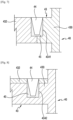
- FIG. 6 is a cross-sectional view illustrating a different conductive structure formed on a portion of a side member according to an embodiment of the disclosure.
- a conductive structure formed on the first portion 43 may be disposed between the metal structure 430 and a non-metal structure 432.
- a housing groove 4340 may be formed on a boundary portion of the metal structure 430 and the non-metal structure 423, and the conductive body 44 may be press-fitted to the housing groove 4340.
- the adhesive 45 may be applied to the housing groove 434 before the conductive member is press-fitted.
- the metal structure 430 may be a portion of a side member (e.g., the lateral bezel structure 118 of FIG. 1 ) operating as an antenna radiator
- the non-metal structure 432 may be a portion of a support member (e.g., the first support member 311 of FIG. 3 ) as a polymer material.
- FIGS. 7, 8 , 9A, and 9B are cross-sectional views illustrating different conductive structures formed on a portion of a side member according to various embodiments of the disclosure.
- a conductive structure formed on the first portion 43 of the side member 40 may be located between the metal structure 430 located at one side and the non-metal structure 432 located at the other side.
- a housing groove 4341 may be formed on a boundary portion of the metal structure 430 and the non-metal structure 432.
- the housed conductive body 44 may be electrically coupled to the metal structure 430.
- the metal structure 430 may be a portion of the side member 40 operating as an antenna radiator, and the non-metal structure 432 may be a portion of a support member as a polymer material.
- the metal structure 430 may be disposed in parallel with the non-metal structure 432, as a feeding portion (e.g., the feeding portion 41 of FIG. 4 ) or ground portion (e.g., the ground portion 42 of FIG. 4 ) of the side member 40 operating as an antenna radiator.
- a feeding portion e.g., the feeding portion 41 of FIG. 4
- ground portion e.g., the ground portion 42 of FIG. 4
- a conductive structure formed on the first portion 43 of the side member 40 may include the metal structure 430 located at an upper portion, the non-metal structure 432 located at a lower portion, a housing groove 4342 formed across the upper metal structure 430 and the non-metal structure 432, and the conductive body 44 press-fitted to the housing groove 4342.
- the metal structure 430 may be a portion of the side member 40 of the antenna radiator, and the non-metal structure 432 may be a portion of a support member as a polymer material.
- the metal structure 430 may be disposed below the non-metal structure 432, as the feeding portion 41 or ground portion 42 of the side member 40 operating as the antenna radiator.
- the metal structure 430 and the non-metal structure 432 which is located at the lower portion may be configured by changing their locations from each other.
- the conductive structure formed on the first portion 43 of the side member 40 may be located between the metal structure 430 of the stepped metal structure 430 adjacent to the side member 40 located at an exterior and the non-metal structure 432 bonded to the metal structure 430.
- a housing groove 4343 may be formed on a boundary portion of the stepped shaped metal structure 430 adjacent to the exterior and the non-metal structure 432.
- the housed conductive body 44 may be electrically coupled to the metal structure 430.
- the conductive structure may include the housing groove 4343 formed across the metal structure 430 and the non-metal structure 432, and the conductive body 44 press-fitted to the housing groove 4343.
- the metal structure 430 may be a portion of the side member 40 of the antenna radiator, and the non-metal structure 432 may be a portion of a support member as a polymer material.
- the metal structure 430 may be disposed in parallel with the non-metal structure 432, as a feeding portion (e.g., the feeding portion 41 of FIG. 4 ) or ground portion (e.g., the ground portion 42 of FIG. 4 ) operating as the antenna radiator.
- a conductive structure may be formed directly on the side member 40.
- the side member 40 may include an inner face 40a and an outer face 40b, and a housing groove 4344 to which the conductive body 44 is press-fitted may be formed on the inner face 40a.
- the housing groove 4344 may be formed to be recessed in a direction perpendicular to each of first and second directions 1 and 2.
- the housing groove 4344 may have a cylindrical shape, a conical shape, or a truncated conical shape.
- a space between an inner portion of the housing groove 4344 and the conductive body 44 may be filled with the adhesive 45.
- the adhesive 45 may include a conductive material.
- a connection area may be increased between the conductive body 44 and the side member 40 due to the adhesive 45 including the conductive material.
- the housing groove 434 may be filled with the adhesive 45 to serve for a sealing function of the housing groove 434.
- the conductive structure formed through the press-fit process between the conductive body 44 and the housing groove 434 may not only be utilized as a connection structure between a printed circuit board and a side member operating as an antenna radiator but also be equally applied to a conductive structure for an electrical connection between the printed circuit board and a circuitry, a conductive structure for an electronic connection between the printed circuit board and an antenna such as NFC, or a conductive structure for an electrical connection between the printed circuit board and a portion of a conductive structure disposed inside a housing.
- a conductive structure formed between the conductive body 44 and the housing groove 434 through the press-fit process may be equally applied to a conductive structure for an electrical connection between the printed circuit board and a metallic structure disposed to the rear side (e.g., the metallic back cover) of the electronic device.
- FIGS. 10A to 10E are cross-sectional views sequentially illustrating methods of manufacturing a conductive structure disposed to a side member according to various embodiments of the disclosure.
- the conductive structure may be a device for electrically connecting a first portion (e.g., the first portion 43 of FIG. 4 ) of a side member operating as an antenna radiator to a connection terminal (e.g., the connection terminal 46 of FIG. 5 ) mounted on the printed circuit board 50.
- the housing groove 434 may be formed on the metal structure 430 according to an embodiment through a drill (not shown) or CNC processing.
- the housing groove 434 may include a cylindrical shape.
- the reference numeral 432 may refer to a non-metal structure.
- a dispenser D may be located on the housing groove 434 according to an embodiment, and thereafter an adhesive solution B may be applied into the housing groove 434.
- the adhesive solution B to be applied is necessary in amount as much as filling part of a volume of the housing groove 434.
- the adhesive solution B may include a conductive material.
- the applied adhesive solution B may be part of a conductive structure after curing, and may be part of a sealing structure which seals the housing groove 434.
- the adhesive solution B may be cured through natural curing, moisture curing, or thermal curing.
- a prepared conductive member 440 may be picked to be disposed on the housing groove 434.
- the prepared conductive member 440 may include the conductive body 44 and a conductive inserting head 441.
- the conductive body 44 may be a portion which is conducted by being inserted to the housing groove 434, and the conductive inserting head 441 may be a portion to be inserted to a press-fit device (not shown).
- the conductive inserting head 441 may be extended from the conductive body 44.
- a diameter of the conductive inserting head 441 may be greater than a diameter of the housing groove 434.
- the conductive body 44 may be formed in any one of a cylindrical shape, a truncated conical shape, a square pillar shape, a polygonal pillar shape, and a polygonal pyramid shape.
- the conductive body 44 may use a material having lower strength or hardness than a metal structure having the housing groove 434 formed thereon.
- the conductive structure (e.g. metal structure 430) and the conductive body 44 may be formed of identical or different materials.
- a prepared conductive member may be press-fitted to the housing groove 434 by using a press-fit device.
- a press-fit process only the conductive body 44 of the conductive member may be press-fitted to the housing groove 434 and thus may be closely in contact with an inner face of the housing groove 434.
- a space between the conductive body 44 and an inner face of the housing groove 434 may be filled with the adhesive 45.
- An inner portion of the housing groove 434 may be sealed by the applied adhesive 45.
- the conductive inserting head 441 of the press-fitted conductive member 440 may be cut, and a cut face of the conductive body 44 may be a connection face.
- the cut face may be co-planner with one face of the metal structure 430.
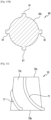
- FIG. 11A is a front view illustrating a conductive body of a conductive member according to an embodiment of the disclosure.
- FIG. 11B is a cross-sectional view, cut along the ling A-A' of FIG. 11A according to an embodiment of the disclosure.
- a conductive body 60 of a conductive member may have at least one protrusion 61 formed on an outer circumferential face 60c.
- the at least one protrusion 61 is for facilitating deformation in a press-fit process of the conductive member.
- the deformation of the protrusion 61 may result in improvement of a mechanical and electrical contact between a housing groove (e.g., the housing groove 434 of FIG. 6 ) and the conductive body 60.
- the conductive body 60 of a cylindrical shape, a square pyramid shape, a polygonal pyramid shape, or a truncated conical shape may include a first face 60a facing the housing groove and a second face 60b facing away from the first face 60a.
- the at least one protrusion 61 may be deformed by being pressed with the housing groove in a press-fit process, so that a metal structure (e.g., the metal structure 430 of FIG. 5 ) of a first portion is closely in contact with the conductive body 44.
- the at least one protrusion 61 may be extended from the first face 60a to the second face 60b. According to an embodiment, the at least one protrusion 61 may be extended in a linear shape. According to an embodiment, a thickness and width of each of the protrusions 61 may be formed to be uniform or not uniform. According to an embodiment, each of the protrusions 61 may protrude outwardly from the outer circumferential face 60c of the conductive body 60.
- the outer circumferential face of the conductive body 60 may be coated with any one material among metal with corrosion resistance, polymer having conductivity, and an inorganic material having conductivity.
- the outer face may include the first face 60a, the second face 60b, and the outer circumferential face 60c.
- FIG. 12 is a front view illustrating a conductive body of a conductive member according to an embodiment of the disclosure.
- a conductive body 70 of a conductive member may have at least one protrusion 71 formed on an outer circumferential face 70c.
- the conductive body 70 may include a first face 70a facing a housing groove and a second face 70b facing away from the first face 70a.
- the at least one protrusion 71 may be deformed by being pressed with the housing groove in a press-fit process so as to increase a contact area between a metal structure (e.g., the metal structure 430 of FIG. 5 ) and the conductive body 70.
- the at least one protrusion 71 may be extended from the first face 70a to the second face 70b. According to an embodiment, the at least one protrusion 71 may be extended in a curved shape. According to an embodiment, the at least one protrusion 71 may be formed in a spiral shape on the outer circumferential face 70c of the conductive body 70. According to an embodiment, a thickness and width of each of the protrusions 71 may be formed to be uniform or not uniform. According to an embodiment, each of the protrusions 71 may protrude outwardly from the outer circumferential face 70c of the conductive body 70.
- the outer circumferential face of the conductive body 70 may be coated with any one material among metal with corrosion resistance, polymer having conductivity, and an inorganic material having conductivity.
- the outer face may include the first face 70a, the second face 70b, and the outer circumferential face 70c.
- FIG. 13A is a front view illustrating a conductive body of a conductive member according to an embodiment of the disclosure.
- FIG. 13B is a cross-sectional view, cut along the line B-B' of FIG. 13A according to an embodiment of the disclosure.
- a conductive body 80 may include a bottom portion 80a and a top portion 80b.
- the bottom portion 80a may be formed to be flat, and thus may facilitate to ensure flatness when a housing groove is press-fitted.
- the conductive body 80 may have at least one protrusion 81 formed partially on an outer circumferential face 80c.
- four protrusions 81 may be formed symmetrically on the outer circumferential face 80c of the conductive body 80.
- the at least one protrusion 81 may be extended from the outer circumferential face 80c of the conductive body in a linear shape from the top portion 80b to the bottom portion 80a.
- each of the protrusions 81 may be formed with equal intervals on the outer circumferential face.
- the protrusion 81 may process a corner portion 81d in a round shape so that the conductive body 80 is easily deformed, and a burr shape is minimized when the conductive body 80 is deformed.
- the conductive body 80 may form a first face 81e of the protrusion 81 in a linear shape to increase a contact area with respect to a housing groove.
- the conductive body 80 may form tapered first and second inclined faces 80f and 80g to facilitate location correction when it is press-fitted with the conductive body.
- the first inclined face 80f may be produced in such a shape that a side face of the bottom portion 80a is an inclined face or a tapered face.
- the second inclined face 80g may be formed at a lower end of each of the protrusions 81.
Landscapes
- Engineering & Computer Science (AREA)
- Microelectronics & Electronic Packaging (AREA)
- Signal Processing (AREA)
- Manufacturing & Machinery (AREA)
- Computer Networks & Wireless Communication (AREA)
- Casings For Electric Apparatus (AREA)
- Telephone Set Structure (AREA)
Claims (14)
- Elektronische Vorrichtung, Folgendes umfassend:ein Gehäuse (110), Folgendes umfassend:eine Anzeige (101, 330);eine vordere Platte (102, 320), die einer ersten Richtung zugewandt ist,eine hintere Platte (111, 380), die einer zweiten, der ersten Richtung entgegengesetzten Richtung zugewandt ist, undein Seitenelement (40), das zumindest einen Teil eines Raums zwischen der vorderen Platte (320) und der hinteren Platte (380) umgibt und als Antennenstrahler wirkt, indem es zumindest teilweise aus einem Metallmaterial (400) ausgebildet ist;ein Trägerelement (311), Folgendes umfassend:eine erste Fläche, die der ersten Richtung zugewandt ist, undeine zweite, der zweiten Richtung zugewandte Fläche, die zwischen der Anzeige (330) und der hinteren Platte (380) angeordnet ist, die Anzeige auf der ersten Fläche trägt und mit einem Teil des Seitenelements (40) verbunden ist;eine Leiterplatte (340, 50), die zwischen dem Trägerelement (311) und der hinteren Platte (380) angeordnet ist und auf der zweiten Fläche gestützt wird;eine Gehäusenut (434), die an einem ersten Abschnitt (43) des Seitenelements (40) ausgebildet ist;einen leitenden Körper (44), der durch Einpressen mit der Gehäusenut (434) verbunden ist; undeine Anschlussklemme (46), die auf der Leiterplatte (50) angeordnet ist und den eingepressten leitenden Körper elektrisch mit der Leiterplatte (50) koppelt.
- Elektronische Vorrichtung nach Anspruch 1, wobei der leitende Körper (44) in einer zylindrischen Form, einer kegelstumpfförmigen Form, einer quadratischen Pyramidenform oder einer polygonalen Pyramidenform ausgebildet ist.
- Elektronische Vorrichtung nach Anspruch 1, wobei der leitende Körper (44, 60, 70) mindestens einen Vorsprung (61, 71) aufweist, der auf einer äußeren Umfangsfläche (60c, 70c) desselben ausgebildet ist.
- Elektronische Vorrichtung nach Anspruch 3,wobei beim Einpressen des leitenden Körpers (44, 60, 70) der mindestens eine Vorsprung (61) aufgrund des Pressens mit der Gehäusenut (434) verformt wird, undwobei der mindestens eine Vorsprung (61) zwischen der Gehäusenut (434) und dem leitenden Körper (44, 60, 70) angebracht ist.
- Elektronische Vorrichtung nach Anspruch 3,wobei der mindestens eine Vorsprung (61) Folgendes umfasst:eine erste Fläche (60a), die der Gehäusenut (434) zugewandt ist, undeine zweite Fläche (60b), die von der ersten Fläche (70a) abgewandt ist,wobei jeder der Vorsprünge (61) an einer äußeren Umfangsfläche (60c) des leitenden Körpers (60) ausgebildet ist, undwobei sich jeder der Vorsprünge (61) linear von der ersten Fläche (60a) zur zweiten Fläche (60b) erstreckt.
- Elektronische Vorrichtung nach Anspruch 3,wobei der mindestens eine Vorsprung (71) Folgendes umfasst:eine erste Fläche (70a), die der Gehäusenut (434) zugewandt ist, undeine zweite Fläche (70b), die von der ersten Fläche (70a) abgewandt ist,wobei der mindestens eine Vorsprung (71) an einer äußeren Umfangsfläche (70c) des leitenden Körpers (70) ausgebildet ist, undwobei sich der mindestens eine Vorsprung (71) in einer gekrümmten Form von der ersten Fläche (70a) zu der zweiten Fläche (70b) erstreckt.
- Elektronische Vorrichtung nach Anspruch 6, wobei die gekrümmte Form eine Spiralform umfasst.
- Elektronische Vorrichtung nach Anspruch 1, wobei der leitende Körper (44) mit einem von einem Metall mit Korrosionsbeständigkeit, einem Polymer mit Leitfähigkeit oder einem anorganischen Material mit Leitfähigkeit beschichtet ist.
- Elektronische Vorrichtung nach Anspruch 1, wobei die Gehäusenut (434) in einer im Wesentlichen zylindrischen Form ausgebildet ist.
- Elektronische Vorrichtung nach Anspruch 1,wobei der erste Abschnitt (43) des Seitenelements (40) Folgendes umfasst:eine erste Fläche (43a), die der ersten Richtung zugewandt ist; undeine zweite Fläche (43b), die der zweiten Richtung zugewandt ist, undwobei die Gehäusenut (434) in der ersten Richtung auf der zweiten Fläche (43b) vertieft ist.
- Elektronische Vorrichtung nach Anspruch 1, wobei die Gehäusenut (434) einen Klebstoff (45) umfasst, und wobei der Klebstoff (45) zwischen der Gehäusenut (434) und dem eingepressten leitfähigen Körper aufgebracht ist.
- Elektronische Vorrichtung nach Anspruch 11, wobei der in der Gehäusenut (434) aufgebrachte Klebstoff (45) zur Abdichtung des eingepressten leitfähigen Körpers dient,
wobei der Klebstoff (45) ein leitfähiges Material enthält. - Elektronische Vorrichtung nach Anspruch 1, wobei der erste Abschnitt (43) des Seitenelements (40) einer Richtung zugewandt ist, die senkrecht zu der ersten bzw. zweiten Richtung verläuft,wobei sich der erste Abschnitt (43) des Seitenelements (40) von dem Seitenelement (40) in Richtung des Inneren des Gehäuses erstreckt,wobei der erste Abschnitt (43) des Seitenelements (40) als Zuführungsabschnitt (41) oder als Grundabschnitt (42) wirkt.
- Elektronische Vorrichtung nach Anspruch 1,wobei der erste Abschnitt (43) des Seitenelements (40) Folgendes umfasst:eine Metallstruktur (430), die sich von dem an der Außenseite befindlichen Seitenelement in Richtung des Inneren des Gehäuses erstreckt, undeine nichtmetallische Struktur (432), die sich von der Metallstruktur (430) aus erstreckt und mit der Metallstruktur (430) verbunden ist, undwobei die Gehäusenut (434) an der Metallstruktur (430) und der Nichtmetallstruktur (432) ausgebildet ist, oder die Gehäusenut (434) an der Metallstruktur (430) ausgebildet ist.
Applications Claiming Priority (2)
| Application Number | Priority Date | Filing Date | Title |
|---|---|---|---|
| KR1020190066559A KR102752225B1 (ko) | 2019-06-05 | 2019-06-05 | 지지 부재의 도전 구조를 포함하는 전자 장치 |
| PCT/KR2020/007311 WO2020246841A1 (en) | 2019-06-05 | 2020-06-05 | Electronic device having conductive structure of supporting member |
Publications (3)
| Publication Number | Publication Date |
|---|---|
| EP3939244A1 EP3939244A1 (de) | 2022-01-19 |
| EP3939244A4 EP3939244A4 (de) | 2022-05-04 |
| EP3939244B1 true EP3939244B1 (de) | 2024-07-31 |
Family
ID=73650425
Family Applications (1)
| Application Number | Title | Priority Date | Filing Date |
|---|---|---|---|
| EP20818138.8A Active EP3939244B1 (de) | 2019-06-05 | 2020-06-05 | Elektronische vorrichtung mit leitender struktur eines trägerelements |
Country Status (4)
| Country | Link |
|---|---|
| US (1) | US11457528B2 (de) |
| EP (1) | EP3939244B1 (de) |
| KR (1) | KR102752225B1 (de) |
| WO (1) | WO2020246841A1 (de) |
Families Citing this family (5)
| Publication number | Priority date | Publication date | Assignee | Title |
|---|---|---|---|---|
| KR20220150053A (ko) * | 2021-05-03 | 2022-11-10 | 삼성전자주식회사 | 지지 부재를 포함하는 전자 장치 |
| WO2024014656A1 (ko) | 2022-07-12 | 2024-01-18 | 삼성전자 주식회사 | 서로 체결된 이종 금속들을 가지는 하우징을 포함하는 전자 장치 |
| CN220674174U (zh) * | 2023-07-31 | 2024-03-26 | 荣耀终端有限公司 | 一种中框结构件和电子设备 |
| KR20260034293A (ko) * | 2024-09-04 | 2026-03-11 | 삼성전자주식회사 | 안테나를 포함하는 전자 장치 |
| WO2026095343A1 (ko) * | 2024-10-31 | 2026-05-07 | 삼성전자 주식회사 | 전도성 접촉 부재를 포함하는 전자 장치 |
Family Cites Families (12)
| Publication number | Priority date | Publication date | Assignee | Title |
|---|---|---|---|---|
| US7933123B2 (en) * | 2008-04-11 | 2011-04-26 | Apple Inc. | Portable electronic device with two-piece housing |
| KR100935954B1 (ko) * | 2009-04-23 | 2010-01-12 | 삼성전기주식회사 | 전자장치 케이스, 그 제조방법 및 제조금형, 이동통신 단말기 |
| KR101132698B1 (ko) * | 2009-06-26 | 2012-04-03 | 주식회사 이엠따블유 | 내장형 안테나, 내장형 안테나의 접속 구조 및 그 제조 방법 |
| US9293827B2 (en) * | 2010-05-10 | 2016-03-22 | Samsung Electronics Co., Ltd. | Communication terminal and antenna apparatus thereof |
| WO2012030010A1 (ko) * | 2010-09-03 | 2012-03-08 | 엑스지 솔루션스 엘엘씨 | 모바일 기기의 송수신 감도 향상을 위한 안테나 부스터 케이스 |
| KR101400846B1 (ko) * | 2012-12-04 | 2014-05-29 | 주식회사 에이스테크놀로지 | 방수용 휴대폰에 내장되는 내장형 안테나 장치 |
| KR20150028112A (ko) * | 2013-09-05 | 2015-03-13 | 주식회사 팬택 | 부품 연결 부재, 이를 포함하는 이동 통신 단말기 및 이동 통신 단말기 제조 방법 |
| KR102208686B1 (ko) * | 2014-08-11 | 2021-01-28 | 삼성전자주식회사 | 전자 장치 및 그 제작 방법 |
| KR101624192B1 (ko) * | 2014-11-14 | 2016-05-26 | 김우중 | 금속 테두리를 갖는 이동통신 단말기용 안테나의 제작방법, 이에 의해 제조된 이동통신 단말기용 안테나 및 이를 갖는 이동통신 단말기 |
| KR101632205B1 (ko) * | 2014-11-26 | 2016-06-22 | 김우중 | 갈바닉 내부식특성을 향상시킨 이동통신 단말기용 안테나의 제작방법, 이에 의해 제조된 이동통신 단말기용 케이스 및 이를 갖는 이동통신 단말기 |
| KR102400529B1 (ko) | 2015-10-26 | 2022-05-20 | 삼성전자주식회사 | 금속 케이스를 구비한 전자기기 및 이에 사용되는 금속 케이스 |
| KR102527317B1 (ko) * | 2016-08-30 | 2023-05-03 | 삼성전자주식회사 | 금속 패드가 부착된 금속 케이스를 구비한 전자기기 |
-
2019
- 2019-06-05 KR KR1020190066559A patent/KR102752225B1/ko active Active
-
2020
- 2020-06-05 US US16/894,094 patent/US11457528B2/en active Active
- 2020-06-05 WO PCT/KR2020/007311 patent/WO2020246841A1/en not_active Ceased
- 2020-06-05 EP EP20818138.8A patent/EP3939244B1/de active Active
Also Published As
| Publication number | Publication date |
|---|---|
| US20200389970A1 (en) | 2020-12-10 |
| US11457528B2 (en) | 2022-09-27 |
| EP3939244A4 (de) | 2022-05-04 |
| WO2020246841A1 (en) | 2020-12-10 |
| KR20200139977A (ko) | 2020-12-15 |
| KR102752225B1 (ko) | 2025-01-10 |
| EP3939244A1 (de) | 2022-01-19 |
Similar Documents
| Publication | Publication Date | Title |
|---|---|---|
| US11457528B2 (en) | Electronic device having conductive structure of supporting member | |
| EP3763110B1 (de) | Elektronische vorrichtung mit gehäuse und verfahren zur herstellung des gehäuses | |
| US10972591B2 (en) | Housing, method of producing the same, and electronic device including the same | |
| US11604256B2 (en) | Electronic device with heat-radiant structure | |
| US11402872B2 (en) | Electronic device with bonding structure | |
| EP3689116B1 (de) | Elektronische vorrichtung mit wasserdichter struktur | |
| KR20200100294A (ko) | 센서 키 조립체의 방수 구조를 포함하는 전자 장치 | |
| US11146718B2 (en) | Camera assembly and electronic device including the same | |
| EP3925201B1 (de) | Elektronische vorrichtung mit anzeige | |
| US11756752B2 (en) | Electronic device | |
| KR102642314B1 (ko) | 방수구조를 갖는 전자장치 | |
| KR20220073697A (ko) | 전자 장치 | |
| EP3688980B1 (de) | Kameramodul mit elastizität und mobile vorrichtung damit | |
| US20220374051A1 (en) | Electronic device including printed circuit board | |
| US10923799B2 (en) | Antenna structure and electronic device therewith | |
| EP3755133B1 (de) | Elektronische vorrichtung mit abschirmdosenstruktur | |
| KR102929325B1 (ko) | 내충격성 보강 구조체를 포함하는 전자 장치 | |
| KR20220033181A (ko) | 안테나 및 그것을 포함하는 전자 장치 | |
| US20230028842A1 (en) | Electronic device frame and electronic device including the same | |
| KR20260007942A (ko) | 이종 소재를 포함하는 하우징 부품 |
Legal Events
| Date | Code | Title | Description |
|---|---|---|---|
| STAA | Information on the status of an ep patent application or granted ep patent |
Free format text: STATUS: THE INTERNATIONAL PUBLICATION HAS BEEN MADE |
|
| PUAI | Public reference made under article 153(3) epc to a published international application that has entered the european phase |
Free format text: ORIGINAL CODE: 0009012 |
|
| STAA | Information on the status of an ep patent application or granted ep patent |
Free format text: STATUS: REQUEST FOR EXAMINATION WAS MADE |
|
| 17P | Request for examination filed |
Effective date: 20211015 |
|
| AK | Designated contracting states |
Kind code of ref document: A1 Designated state(s): AL AT BE BG CH CY CZ DE DK EE ES FI FR GB GR HR HU IE IS IT LI LT LU LV MC MK MT NL NO PL PT RO RS SE SI SK SM TR |
|
| A4 | Supplementary search report drawn up and despatched |
Effective date: 20220404 |
|
| RIC1 | Information provided on ipc code assigned before grant |
Ipc: H05K 1/02 20060101ALI20220328BHEP Ipc: H01Q 1/36 20060101ALI20220328BHEP Ipc: H01Q 1/24 20060101AFI20220328BHEP |
|
| DAV | Request for validation of the european patent (deleted) | ||
| DAX | Request for extension of the european patent (deleted) | ||
| REG | Reference to a national code |
Ref country code: DE Ref legal event code: R079 Free format text: PREVIOUS MAIN CLASS: H04M0001020000 Ipc: H01Q0001240000 Ref country code: DE Ref legal event code: R079 Ref document number: 602020034985 Country of ref document: DE Free format text: PREVIOUS MAIN CLASS: H04M0001020000 Ipc: H01Q0001240000 |
|
| GRAP | Despatch of communication of intention to grant a patent |
Free format text: ORIGINAL CODE: EPIDOSNIGR1 |
|
| STAA | Information on the status of an ep patent application or granted ep patent |
Free format text: STATUS: GRANT OF PATENT IS INTENDED |
|
| RIC1 | Information provided on ipc code assigned before grant |
Ipc: H05K 1/02 20060101ALI20240125BHEP Ipc: H01Q 1/36 20060101ALI20240125BHEP Ipc: H01Q 1/24 20060101AFI20240125BHEP |
|
| INTG | Intention to grant announced |
Effective date: 20240214 |
|
| GRAS | Grant fee paid |
Free format text: ORIGINAL CODE: EPIDOSNIGR3 |
|
| GRAA | (expected) grant |
Free format text: ORIGINAL CODE: 0009210 |
|
| STAA | Information on the status of an ep patent application or granted ep patent |
Free format text: STATUS: THE PATENT HAS BEEN GRANTED |
|
| AK | Designated contracting states |
Kind code of ref document: B1 Designated state(s): AL AT BE BG CH CY CZ DE DK EE ES FI FR GB GR HR HU IE IS IT LI LT LU LV MC MK MT NL NO PL PT RO RS SE SI SK SM TR |
|
| REG | Reference to a national code |
Ref country code: CH Ref legal event code: EP Ref country code: GB Ref legal event code: FG4D |
|
| REG | Reference to a national code |
Ref country code: DE Ref legal event code: R096 Ref document number: 602020034985 Country of ref document: DE |
|
| REG | Reference to a national code |
Ref country code: IE Ref legal event code: FG4D |
|
| REG | Reference to a national code |
Ref country code: LT Ref legal event code: MG9D |
|
| REG | Reference to a national code |
Ref country code: NL Ref legal event code: MP Effective date: 20240731 |
|
| PG25 | Lapsed in a contracting state [announced via postgrant information from national office to epo] |
Ref country code: PT Free format text: LAPSE BECAUSE OF FAILURE TO SUBMIT A TRANSLATION OF THE DESCRIPTION OR TO PAY THE FEE WITHIN THE PRESCRIBED TIME-LIMIT Effective date: 20241202 |
|
| REG | Reference to a national code |
Ref country code: AT Ref legal event code: MK05 Ref document number: 1709381 Country of ref document: AT Kind code of ref document: T Effective date: 20240731 |
|
| PG25 | Lapsed in a contracting state [announced via postgrant information from national office to epo] |
Ref country code: PT Free format text: LAPSE BECAUSE OF FAILURE TO SUBMIT A TRANSLATION OF THE DESCRIPTION OR TO PAY THE FEE WITHIN THE PRESCRIBED TIME-LIMIT Effective date: 20241202 |
|
| PG25 | Lapsed in a contracting state [announced via postgrant information from national office to epo] |
Ref country code: NO Free format text: LAPSE BECAUSE OF FAILURE TO SUBMIT A TRANSLATION OF THE DESCRIPTION OR TO PAY THE FEE WITHIN THE PRESCRIBED TIME-LIMIT Effective date: 20241031 |
|
| PG25 | Lapsed in a contracting state [announced via postgrant information from national office to epo] |
Ref country code: FI Free format text: LAPSE BECAUSE OF FAILURE TO SUBMIT A TRANSLATION OF THE DESCRIPTION OR TO PAY THE FEE WITHIN THE PRESCRIBED TIME-LIMIT Effective date: 20240731 Ref country code: NL Free format text: LAPSE BECAUSE OF FAILURE TO SUBMIT A TRANSLATION OF THE DESCRIPTION OR TO PAY THE FEE WITHIN THE PRESCRIBED TIME-LIMIT Effective date: 20240731 Ref country code: GR Free format text: LAPSE BECAUSE OF FAILURE TO SUBMIT A TRANSLATION OF THE DESCRIPTION OR TO PAY THE FEE WITHIN THE PRESCRIBED TIME-LIMIT Effective date: 20241101 Ref country code: PL Free format text: LAPSE BECAUSE OF FAILURE TO SUBMIT A TRANSLATION OF THE DESCRIPTION OR TO PAY THE FEE WITHIN THE PRESCRIBED TIME-LIMIT Effective date: 20240731 |
|
| PG25 | Lapsed in a contracting state [announced via postgrant information from national office to epo] |
Ref country code: BG Free format text: LAPSE BECAUSE OF FAILURE TO SUBMIT A TRANSLATION OF THE DESCRIPTION OR TO PAY THE FEE WITHIN THE PRESCRIBED TIME-LIMIT Effective date: 20240731 |
|
| PG25 | Lapsed in a contracting state [announced via postgrant information from national office to epo] |
Ref country code: LV Free format text: LAPSE BECAUSE OF FAILURE TO SUBMIT A TRANSLATION OF THE DESCRIPTION OR TO PAY THE FEE WITHIN THE PRESCRIBED TIME-LIMIT Effective date: 20240731 |
|
| PG25 | Lapsed in a contracting state [announced via postgrant information from national office to epo] |
Ref country code: AT Free format text: LAPSE BECAUSE OF FAILURE TO SUBMIT A TRANSLATION OF THE DESCRIPTION OR TO PAY THE FEE WITHIN THE PRESCRIBED TIME-LIMIT Effective date: 20240731 Ref country code: IS Free format text: LAPSE BECAUSE OF FAILURE TO SUBMIT A TRANSLATION OF THE DESCRIPTION OR TO PAY THE FEE WITHIN THE PRESCRIBED TIME-LIMIT Effective date: 20241130 |
|
| PG25 | Lapsed in a contracting state [announced via postgrant information from national office to epo] |
Ref country code: HR Free format text: LAPSE BECAUSE OF FAILURE TO SUBMIT A TRANSLATION OF THE DESCRIPTION OR TO PAY THE FEE WITHIN THE PRESCRIBED TIME-LIMIT Effective date: 20240731 |
|
| PG25 | Lapsed in a contracting state [announced via postgrant information from national office to epo] |
Ref country code: RS Free format text: LAPSE BECAUSE OF FAILURE TO SUBMIT A TRANSLATION OF THE DESCRIPTION OR TO PAY THE FEE WITHIN THE PRESCRIBED TIME-LIMIT Effective date: 20241031 Ref country code: ES Free format text: LAPSE BECAUSE OF FAILURE TO SUBMIT A TRANSLATION OF THE DESCRIPTION OR TO PAY THE FEE WITHIN THE PRESCRIBED TIME-LIMIT Effective date: 20240731 |
|
| PG25 | Lapsed in a contracting state [announced via postgrant information from national office to epo] |
Ref country code: RS Free format text: LAPSE BECAUSE OF FAILURE TO SUBMIT A TRANSLATION OF THE DESCRIPTION OR TO PAY THE FEE WITHIN THE PRESCRIBED TIME-LIMIT Effective date: 20241031 Ref country code: PL Free format text: LAPSE BECAUSE OF FAILURE TO SUBMIT A TRANSLATION OF THE DESCRIPTION OR TO PAY THE FEE WITHIN THE PRESCRIBED TIME-LIMIT Effective date: 20240731 Ref country code: NO Free format text: LAPSE BECAUSE OF FAILURE TO SUBMIT A TRANSLATION OF THE DESCRIPTION OR TO PAY THE FEE WITHIN THE PRESCRIBED TIME-LIMIT Effective date: 20241031 Ref country code: NL Free format text: LAPSE BECAUSE OF FAILURE TO SUBMIT A TRANSLATION OF THE DESCRIPTION OR TO PAY THE FEE WITHIN THE PRESCRIBED TIME-LIMIT Effective date: 20240731 Ref country code: LV Free format text: LAPSE BECAUSE OF FAILURE TO SUBMIT A TRANSLATION OF THE DESCRIPTION OR TO PAY THE FEE WITHIN THE PRESCRIBED TIME-LIMIT Effective date: 20240731 Ref country code: IS Free format text: LAPSE BECAUSE OF FAILURE TO SUBMIT A TRANSLATION OF THE DESCRIPTION OR TO PAY THE FEE WITHIN THE PRESCRIBED TIME-LIMIT Effective date: 20241130 Ref country code: HR Free format text: LAPSE BECAUSE OF FAILURE TO SUBMIT A TRANSLATION OF THE DESCRIPTION OR TO PAY THE FEE WITHIN THE PRESCRIBED TIME-LIMIT Effective date: 20240731 Ref country code: GR Free format text: LAPSE BECAUSE OF FAILURE TO SUBMIT A TRANSLATION OF THE DESCRIPTION OR TO PAY THE FEE WITHIN THE PRESCRIBED TIME-LIMIT Effective date: 20241101 Ref country code: FI Free format text: LAPSE BECAUSE OF FAILURE TO SUBMIT A TRANSLATION OF THE DESCRIPTION OR TO PAY THE FEE WITHIN THE PRESCRIBED TIME-LIMIT Effective date: 20240731 Ref country code: ES Free format text: LAPSE BECAUSE OF FAILURE TO SUBMIT A TRANSLATION OF THE DESCRIPTION OR TO PAY THE FEE WITHIN THE PRESCRIBED TIME-LIMIT Effective date: 20240731 Ref country code: BG Free format text: LAPSE BECAUSE OF FAILURE TO SUBMIT A TRANSLATION OF THE DESCRIPTION OR TO PAY THE FEE WITHIN THE PRESCRIBED TIME-LIMIT Effective date: 20240731 Ref country code: AT Free format text: LAPSE BECAUSE OF FAILURE TO SUBMIT A TRANSLATION OF THE DESCRIPTION OR TO PAY THE FEE WITHIN THE PRESCRIBED TIME-LIMIT Effective date: 20240731 |
|
| PG25 | Lapsed in a contracting state [announced via postgrant information from national office to epo] |
Ref country code: RO Free format text: LAPSE BECAUSE OF FAILURE TO SUBMIT A TRANSLATION OF THE DESCRIPTION OR TO PAY THE FEE WITHIN THE PRESCRIBED TIME-LIMIT Effective date: 20240731 Ref country code: SM Free format text: LAPSE BECAUSE OF FAILURE TO SUBMIT A TRANSLATION OF THE DESCRIPTION OR TO PAY THE FEE WITHIN THE PRESCRIBED TIME-LIMIT Effective date: 20240731 Ref country code: DK Free format text: LAPSE BECAUSE OF FAILURE TO SUBMIT A TRANSLATION OF THE DESCRIPTION OR TO PAY THE FEE WITHIN THE PRESCRIBED TIME-LIMIT Effective date: 20240731 |
|
| PG25 | Lapsed in a contracting state [announced via postgrant information from national office to epo] |
Ref country code: EE Free format text: LAPSE BECAUSE OF FAILURE TO SUBMIT A TRANSLATION OF THE DESCRIPTION OR TO PAY THE FEE WITHIN THE PRESCRIBED TIME-LIMIT Effective date: 20240731 |
|
| PG25 | Lapsed in a contracting state [announced via postgrant information from national office to epo] |
Ref country code: CZ Free format text: LAPSE BECAUSE OF FAILURE TO SUBMIT A TRANSLATION OF THE DESCRIPTION OR TO PAY THE FEE WITHIN THE PRESCRIBED TIME-LIMIT Effective date: 20240731 |
|
| PG25 | Lapsed in a contracting state [announced via postgrant information from national office to epo] |
Ref country code: IT Free format text: LAPSE BECAUSE OF FAILURE TO SUBMIT A TRANSLATION OF THE DESCRIPTION OR TO PAY THE FEE WITHIN THE PRESCRIBED TIME-LIMIT Effective date: 20240731 Ref country code: SK Free format text: LAPSE BECAUSE OF FAILURE TO SUBMIT A TRANSLATION OF THE DESCRIPTION OR TO PAY THE FEE WITHIN THE PRESCRIBED TIME-LIMIT Effective date: 20240731 |
|
| REG | Reference to a national code |
Ref country code: DE Ref legal event code: R097 Ref document number: 602020034985 Country of ref document: DE |
|
| PLBE | No opposition filed within time limit |
Free format text: ORIGINAL CODE: 0009261 |
|
| STAA | Information on the status of an ep patent application or granted ep patent |
Free format text: STATUS: NO OPPOSITION FILED WITHIN TIME LIMIT |
|
| 26N | No opposition filed |
Effective date: 20250501 |
|
| PGFP | Annual fee paid to national office [announced via postgrant information from national office to epo] |
Ref country code: DE Payment date: 20250520 Year of fee payment: 6 |
|
| PGFP | Annual fee paid to national office [announced via postgrant information from national office to epo] |
Ref country code: GB Payment date: 20250520 Year of fee payment: 6 |
|
| PG25 | Lapsed in a contracting state [announced via postgrant information from national office to epo] |
Ref country code: SE Free format text: LAPSE BECAUSE OF FAILURE TO SUBMIT A TRANSLATION OF THE DESCRIPTION OR TO PAY THE FEE WITHIN THE PRESCRIBED TIME-LIMIT Effective date: 20240731 |
|
| REG | Reference to a national code |
Ref country code: CH Ref legal event code: H13 Free format text: ST27 STATUS EVENT CODE: U-0-0-H10-H13 (AS PROVIDED BY THE NATIONAL OFFICE) Effective date: 20260127 |
|
| PG25 | Lapsed in a contracting state [announced via postgrant information from national office to epo] |
Ref country code: MC Free format text: LAPSE BECAUSE OF FAILURE TO SUBMIT A TRANSLATION OF THE DESCRIPTION OR TO PAY THE FEE WITHIN THE PRESCRIBED TIME-LIMIT Effective date: 20240731 |
|
| PG25 | Lapsed in a contracting state [announced via postgrant information from national office to epo] |
Ref country code: LU Free format text: LAPSE BECAUSE OF NON-PAYMENT OF DUE FEES Effective date: 20250605 |
|
| REG | Reference to a national code |
Ref country code: BE Ref legal event code: MM Effective date: 20250630 |
|
| PG25 | Lapsed in a contracting state [announced via postgrant information from national office to epo] |
Ref country code: IE Free format text: LAPSE BECAUSE OF NON-PAYMENT OF DUE FEES Effective date: 20250605 |
|
| PG25 | Lapsed in a contracting state [announced via postgrant information from national office to epo] |
Ref country code: BE Free format text: LAPSE BECAUSE OF NON-PAYMENT OF DUE FEES Effective date: 20250630 |
|
| PG25 | Lapsed in a contracting state [announced via postgrant information from national office to epo] |
Ref country code: FR Free format text: LAPSE BECAUSE OF NON-PAYMENT OF DUE FEES Effective date: 20250630 |
|
| PG25 | Lapsed in a contracting state [announced via postgrant information from national office to epo] |
Ref country code: CH Free format text: LAPSE BECAUSE OF NON-PAYMENT OF DUE FEES Effective date: 20250630 |