EP3933507A1 - Conveyance apparatus, substrate processing apparatus, and method of manufacturing article - Google Patents
Conveyance apparatus, substrate processing apparatus, and method of manufacturing article Download PDFInfo
- Publication number
- EP3933507A1 EP3933507A1 EP21175861.0A EP21175861A EP3933507A1 EP 3933507 A1 EP3933507 A1 EP 3933507A1 EP 21175861 A EP21175861 A EP 21175861A EP 3933507 A1 EP3933507 A1 EP 3933507A1
- Authority
- EP
- European Patent Office
- Prior art keywords
- hand
- substrate
- main body
- distal end
- substrate chuck
- Prior art date
- Legal status (The legal status is an assumption and is not a legal conclusion. Google has not performed a legal analysis and makes no representation as to the accuracy of the status listed.)
- Pending
Links
- 239000000758 substrate Substances 0.000 title claims abstract description 147
- 238000012545 processing Methods 0.000 title claims description 20
- 238000004519 manufacturing process Methods 0.000 title claims description 11
- 238000001514 detection method Methods 0.000 claims description 4
- 230000003287 optical effect Effects 0.000 description 12
- 101100269850 Caenorhabditis elegans mask-1 gene Proteins 0.000 description 10
- 238000005259 measurement Methods 0.000 description 6
- 238000012986 modification Methods 0.000 description 6
- 230000004048 modification Effects 0.000 description 6
- 238000005286 illumination Methods 0.000 description 4
- 238000000034 method Methods 0.000 description 4
- 229920002120 photoresistant polymer Polymers 0.000 description 4
- 239000003795 chemical substances by application Substances 0.000 description 3
- 239000002245 particle Substances 0.000 description 3
- 238000012937 correction Methods 0.000 description 2
- 230000008021 deposition Effects 0.000 description 2
- 238000000151 deposition Methods 0.000 description 2
- 238000007599 discharging Methods 0.000 description 2
- 238000003384 imaging method Methods 0.000 description 2
- 238000007689 inspection Methods 0.000 description 2
- 239000000463 material Substances 0.000 description 2
- RYGMFSIKBFXOCR-UHFFFAOYSA-N Copper Chemical compound [Cu] RYGMFSIKBFXOCR-UHFFFAOYSA-N 0.000 description 1
- XUIMIQQOPSSXEZ-UHFFFAOYSA-N Silicon Chemical compound [Si] XUIMIQQOPSSXEZ-UHFFFAOYSA-N 0.000 description 1
- 238000007796 conventional method Methods 0.000 description 1
- 229910052802 copper Inorganic materials 0.000 description 1
- 239000010949 copper Substances 0.000 description 1
- 238000006073 displacement reaction Methods 0.000 description 1
- 238000005530 etching Methods 0.000 description 1
- 230000006870 function Effects 0.000 description 1
- 239000011521 glass Substances 0.000 description 1
- 238000001459 lithography Methods 0.000 description 1
- QSHDDOUJBYECFT-UHFFFAOYSA-N mercury Chemical compound [Hg] QSHDDOUJBYECFT-UHFFFAOYSA-N 0.000 description 1
- 229910052753 mercury Inorganic materials 0.000 description 1
- 238000007254 oxidation reaction Methods 0.000 description 1
- 238000004806 packaging method and process Methods 0.000 description 1
- 230000003252 repetitive effect Effects 0.000 description 1
- 239000011347 resin Substances 0.000 description 1
- 229920005989 resin Polymers 0.000 description 1
- 229910052594 sapphire Inorganic materials 0.000 description 1
- 239000010980 sapphire Substances 0.000 description 1
- 239000004065 semiconductor Substances 0.000 description 1
- 229910052710 silicon Inorganic materials 0.000 description 1
- 239000010703 silicon Substances 0.000 description 1
- 238000012546 transfer Methods 0.000 description 1
- 238000007740 vapor deposition Methods 0.000 description 1
Images


Classifications
-
- G—PHYSICS
- G03—PHOTOGRAPHY; CINEMATOGRAPHY; ANALOGOUS TECHNIQUES USING WAVES OTHER THAN OPTICAL WAVES; ELECTROGRAPHY; HOLOGRAPHY
- G03F—PHOTOMECHANICAL PRODUCTION OF TEXTURED OR PATTERNED SURFACES, e.g. FOR PRINTING, FOR PROCESSING OF SEMICONDUCTOR DEVICES; MATERIALS THEREFOR; ORIGINALS THEREFOR; APPARATUS SPECIALLY ADAPTED THEREFOR
- G03F7/00—Photomechanical, e.g. photolithographic, production of textured or patterned surfaces, e.g. printing surfaces; Materials therefor, e.g. comprising photoresists; Apparatus specially adapted therefor
- G03F7/70—Microphotolithographic exposure; Apparatus therefor
- G03F7/70691—Handling of masks or workpieces
- G03F7/70733—Handling masks and workpieces, e.g. exchange of workpiece or mask, transport of workpiece or mask
-
- H—ELECTRICITY
- H01—ELECTRIC ELEMENTS
- H01L—SEMICONDUCTOR DEVICES NOT COVERED BY CLASS H10
- H01L21/00—Processes or apparatus adapted for the manufacture or treatment of semiconductor or solid state devices or of parts thereof
- H01L21/67—Apparatus specially adapted for handling semiconductor or electric solid state devices during manufacture or treatment thereof; Apparatus specially adapted for handling wafers during manufacture or treatment of semiconductor or electric solid state devices or components ; Apparatus not specifically provided for elsewhere
- H01L21/677—Apparatus specially adapted for handling semiconductor or electric solid state devices during manufacture or treatment thereof; Apparatus specially adapted for handling wafers during manufacture or treatment of semiconductor or electric solid state devices or components ; Apparatus not specifically provided for elsewhere for conveying, e.g. between different workstations
- H01L21/67739—Apparatus specially adapted for handling semiconductor or electric solid state devices during manufacture or treatment thereof; Apparatus specially adapted for handling wafers during manufacture or treatment of semiconductor or electric solid state devices or components ; Apparatus not specifically provided for elsewhere for conveying, e.g. between different workstations into and out of processing chamber
- H01L21/67742—Mechanical parts of transfer devices
-
- H—ELECTRICITY
- H01—ELECTRIC ELEMENTS
- H01L—SEMICONDUCTOR DEVICES NOT COVERED BY CLASS H10
- H01L21/00—Processes or apparatus adapted for the manufacture or treatment of semiconductor or solid state devices or of parts thereof
- H01L21/67—Apparatus specially adapted for handling semiconductor or electric solid state devices during manufacture or treatment thereof; Apparatus specially adapted for handling wafers during manufacture or treatment of semiconductor or electric solid state devices or components ; Apparatus not specifically provided for elsewhere
- H01L21/683—Apparatus specially adapted for handling semiconductor or electric solid state devices during manufacture or treatment thereof; Apparatus specially adapted for handling wafers during manufacture or treatment of semiconductor or electric solid state devices or components ; Apparatus not specifically provided for elsewhere for supporting or gripping
- H01L21/687—Apparatus specially adapted for handling semiconductor or electric solid state devices during manufacture or treatment thereof; Apparatus specially adapted for handling wafers during manufacture or treatment of semiconductor or electric solid state devices or components ; Apparatus not specifically provided for elsewhere for supporting or gripping using mechanical means, e.g. chucks, clamps or pinches
- H01L21/68707—Apparatus specially adapted for handling semiconductor or electric solid state devices during manufacture or treatment thereof; Apparatus specially adapted for handling wafers during manufacture or treatment of semiconductor or electric solid state devices or components ; Apparatus not specifically provided for elsewhere for supporting or gripping using mechanical means, e.g. chucks, clamps or pinches the wafers being placed on a robot blade, or gripped by a gripper for conveyance
-
- G—PHYSICS
- G03—PHOTOGRAPHY; CINEMATOGRAPHY; ANALOGOUS TECHNIQUES USING WAVES OTHER THAN OPTICAL WAVES; ELECTROGRAPHY; HOLOGRAPHY
- G03F—PHOTOMECHANICAL PRODUCTION OF TEXTURED OR PATTERNED SURFACES, e.g. FOR PRINTING, FOR PROCESSING OF SEMICONDUCTOR DEVICES; MATERIALS THEREFOR; ORIGINALS THEREFOR; APPARATUS SPECIALLY ADAPTED THEREFOR
- G03F7/00—Photomechanical, e.g. photolithographic, production of textured or patterned surfaces, e.g. printing surfaces; Materials therefor, e.g. comprising photoresists; Apparatus specially adapted therefor
- G03F7/70—Microphotolithographic exposure; Apparatus therefor
- G03F7/70691—Handling of masks or workpieces
- G03F7/707—Chucks, e.g. chucking or un-chucking operations or structural details
-
- G—PHYSICS
- G03—PHOTOGRAPHY; CINEMATOGRAPHY; ANALOGOUS TECHNIQUES USING WAVES OTHER THAN OPTICAL WAVES; ELECTROGRAPHY; HOLOGRAPHY
- G03F—PHOTOMECHANICAL PRODUCTION OF TEXTURED OR PATTERNED SURFACES, e.g. FOR PRINTING, FOR PROCESSING OF SEMICONDUCTOR DEVICES; MATERIALS THEREFOR; ORIGINALS THEREFOR; APPARATUS SPECIALLY ADAPTED THEREFOR
- G03F7/00—Photomechanical, e.g. photolithographic, production of textured or patterned surfaces, e.g. printing surfaces; Materials therefor, e.g. comprising photoresists; Apparatus specially adapted therefor
- G03F7/70—Microphotolithographic exposure; Apparatus therefor
- G03F7/70691—Handling of masks or workpieces
- G03F7/70775—Position control, e.g. interferometers or encoders for determining the stage position
-
- G—PHYSICS
- G03—PHOTOGRAPHY; CINEMATOGRAPHY; ANALOGOUS TECHNIQUES USING WAVES OTHER THAN OPTICAL WAVES; ELECTROGRAPHY; HOLOGRAPHY
- G03F—PHOTOMECHANICAL PRODUCTION OF TEXTURED OR PATTERNED SURFACES, e.g. FOR PRINTING, FOR PROCESSING OF SEMICONDUCTOR DEVICES; MATERIALS THEREFOR; ORIGINALS THEREFOR; APPARATUS SPECIALLY ADAPTED THEREFOR
- G03F9/00—Registration or positioning of originals, masks, frames, photographic sheets or textured or patterned surfaces, e.g. automatically
- G03F9/70—Registration or positioning of originals, masks, frames, photographic sheets or textured or patterned surfaces, e.g. automatically for microlithography
- G03F9/7003—Alignment type or strategy, e.g. leveling, global alignment
- G03F9/7007—Alignment other than original with workpiece
- G03F9/7011—Pre-exposure scan; original with original holder alignment; Prealignment, i.e. workpiece with workpiece holder
-
- H—ELECTRICITY
- H01—ELECTRIC ELEMENTS
- H01L—SEMICONDUCTOR DEVICES NOT COVERED BY CLASS H10
- H01L21/00—Processes or apparatus adapted for the manufacture or treatment of semiconductor or solid state devices or of parts thereof
- H01L21/67—Apparatus specially adapted for handling semiconductor or electric solid state devices during manufacture or treatment thereof; Apparatus specially adapted for handling wafers during manufacture or treatment of semiconductor or electric solid state devices or components ; Apparatus not specifically provided for elsewhere
- H01L21/67005—Apparatus not specifically provided for elsewhere
- H01L21/67242—Apparatus for monitoring, sorting or marking
- H01L21/67259—Position monitoring, e.g. misposition detection or presence detection
- H01L21/67265—Position monitoring, e.g. misposition detection or presence detection of substrates stored in a container, a magazine, a carrier, a boat or the like
-
- H—ELECTRICITY
- H01—ELECTRIC ELEMENTS
- H01L—SEMICONDUCTOR DEVICES NOT COVERED BY CLASS H10
- H01L21/00—Processes or apparatus adapted for the manufacture or treatment of semiconductor or solid state devices or of parts thereof
- H01L21/67—Apparatus specially adapted for handling semiconductor or electric solid state devices during manufacture or treatment thereof; Apparatus specially adapted for handling wafers during manufacture or treatment of semiconductor or electric solid state devices or components ; Apparatus not specifically provided for elsewhere
- H01L21/677—Apparatus specially adapted for handling semiconductor or electric solid state devices during manufacture or treatment thereof; Apparatus specially adapted for handling wafers during manufacture or treatment of semiconductor or electric solid state devices or components ; Apparatus not specifically provided for elsewhere for conveying, e.g. between different workstations
- H01L21/67739—Apparatus specially adapted for handling semiconductor or electric solid state devices during manufacture or treatment thereof; Apparatus specially adapted for handling wafers during manufacture or treatment of semiconductor or electric solid state devices or components ; Apparatus not specifically provided for elsewhere for conveying, e.g. between different workstations into and out of processing chamber
- H01L21/67748—Apparatus specially adapted for handling semiconductor or electric solid state devices during manufacture or treatment thereof; Apparatus specially adapted for handling wafers during manufacture or treatment of semiconductor or electric solid state devices or components ; Apparatus not specifically provided for elsewhere for conveying, e.g. between different workstations into and out of processing chamber horizontal transfer of a single workpiece
-
- H—ELECTRICITY
- H01—ELECTRIC ELEMENTS
- H01L—SEMICONDUCTOR DEVICES NOT COVERED BY CLASS H10
- H01L21/00—Processes or apparatus adapted for the manufacture or treatment of semiconductor or solid state devices or of parts thereof
- H01L21/67—Apparatus specially adapted for handling semiconductor or electric solid state devices during manufacture or treatment thereof; Apparatus specially adapted for handling wafers during manufacture or treatment of semiconductor or electric solid state devices or components ; Apparatus not specifically provided for elsewhere
- H01L21/683—Apparatus specially adapted for handling semiconductor or electric solid state devices during manufacture or treatment thereof; Apparatus specially adapted for handling wafers during manufacture or treatment of semiconductor or electric solid state devices or components ; Apparatus not specifically provided for elsewhere for supporting or gripping
- H01L21/6838—Apparatus specially adapted for handling semiconductor or electric solid state devices during manufacture or treatment thereof; Apparatus specially adapted for handling wafers during manufacture or treatment of semiconductor or electric solid state devices or components ; Apparatus not specifically provided for elsewhere for supporting or gripping with gripping and holding devices using a vacuum; Bernoulli devices
-
- H—ELECTRICITY
- H01—ELECTRIC ELEMENTS
- H01L—SEMICONDUCTOR DEVICES NOT COVERED BY CLASS H10
- H01L21/00—Processes or apparatus adapted for the manufacture or treatment of semiconductor or solid state devices or of parts thereof
- H01L21/67—Apparatus specially adapted for handling semiconductor or electric solid state devices during manufacture or treatment thereof; Apparatus specially adapted for handling wafers during manufacture or treatment of semiconductor or electric solid state devices or components ; Apparatus not specifically provided for elsewhere
- H01L21/683—Apparatus specially adapted for handling semiconductor or electric solid state devices during manufacture or treatment thereof; Apparatus specially adapted for handling wafers during manufacture or treatment of semiconductor or electric solid state devices or components ; Apparatus not specifically provided for elsewhere for supporting or gripping
- H01L21/687—Apparatus specially adapted for handling semiconductor or electric solid state devices during manufacture or treatment thereof; Apparatus specially adapted for handling wafers during manufacture or treatment of semiconductor or electric solid state devices or components ; Apparatus not specifically provided for elsewhere for supporting or gripping using mechanical means, e.g. chucks, clamps or pinches
- H01L21/68714—Apparatus specially adapted for handling semiconductor or electric solid state devices during manufacture or treatment thereof; Apparatus specially adapted for handling wafers during manufacture or treatment of semiconductor or electric solid state devices or components ; Apparatus not specifically provided for elsewhere for supporting or gripping using mechanical means, e.g. chucks, clamps or pinches the wafers being placed on a susceptor, stage or support
- H01L21/68721—Apparatus specially adapted for handling semiconductor or electric solid state devices during manufacture or treatment thereof; Apparatus specially adapted for handling wafers during manufacture or treatment of semiconductor or electric solid state devices or components ; Apparatus not specifically provided for elsewhere for supporting or gripping using mechanical means, e.g. chucks, clamps or pinches the wafers being placed on a susceptor, stage or support characterised by edge clamping, e.g. clamping ring
-
- H—ELECTRICITY
- H01—ELECTRIC ELEMENTS
- H01L—SEMICONDUCTOR DEVICES NOT COVERED BY CLASS H10
- H01L23/00—Details of semiconductor or other solid state devices
- H01L23/544—Marks applied to semiconductor devices or parts, e.g. registration marks, alignment structures, wafer maps
-
- H—ELECTRICITY
- H01—ELECTRIC ELEMENTS
- H01L—SEMICONDUCTOR DEVICES NOT COVERED BY CLASS H10
- H01L2223/00—Details relating to semiconductor or other solid state devices covered by the group H01L23/00
- H01L2223/544—Marks applied to semiconductor devices or parts
- H01L2223/54426—Marks applied to semiconductor devices or parts for alignment
Definitions
- the present invention relates to a conveyance apparatus, a substrate processing apparatus, and a method of manufacturing an article.
- a conveyance apparatus that conveys a substrate or an original is used.
- the conveyance apparatus is required to perform accurate positional control of a substrate or an original as a target object.
- Japanese Patent Laid-Open No. 2000-21956 discloses a rotating stage that supports a substrate and rotates the substrate.
- Japanese Patent No. 5721453 discloses that a substrate (plate-like member) is made to float without contact by discharging gas to the substrate, and a guide which includes a tilted portion is used to relatively displace the substrate and a support portion.
- a substrate chuck conveyance apparatus will be considered here.
- an alignment mechanism as disclosed in Japanese Patent Laid-Open No. 2000-21956 is to be applied in the correction of a rotational shift of the substrate chuck, a plurality of dedicated alignment stages will be needed.
- the substrate stage will need to be drivable at large strokes in the rotational direction, and the substrate stage will need to be upsized.
- Patent No. 5721453 a large amount of gas will need to be supplied, thereby leading an increase in the size and the complexity of the apparatus.
- the present invention provides, for example, a conveyance apparatus that can advantageously perform positional correction of the rotational direction of a substrate chuck in a simple manner.
- the present invention in its first aspect provides an conveyance apparatus as specified in claims 1 to 8.
- the present invention in its second aspect provides a substrate processing apparatus as specified in claims 9 and 10.
- the present invention in its third aspect provides a method of manufacturing an article as specified in claim 11.
- a conveyance apparatus for conveying an object is used in a substrate processing apparatus for processing a substrate.
- An object to be conveyed by the conveyance apparatus can be, for example, a substrate chuck for chucking a substrate.
- the substrate processing apparatus can be any one of, for example, a lithography apparatus (an imprint apparatus, an exposure apparatus, a charged particle beam drawing apparatus, or the like), a deposition apparatus (a CVD apparatus or the like), a processing apparatus (a laser processing apparatus or the like), and an inspection apparatus (an overlay inspection apparatus or the like).
- An imprint apparatus forms a pattern on a substrate by curing an imprint material while bringing a mold (original) into contact with the imprint material supplied on the substrate.
- An exposure apparatus exposes, via an original (reticle) serving as an original mask, a photoresist supplied on a substrate to form a latent image corresponding to the pattern of an original on the photoresist.
- a charged particle beam drawing apparatus uses a charged particle beam to draw a pattern on a photoresist supplied on a substrate and form a latent image on the photoresist.
- a substrate to be processed by such substrate processing apparatuses can be, for example, a silicon wafer, but may also be a glass substrate, a copper substrate, a resin substrate, an SiC substrate, a sapphire substrate, or the like. An example in which the substrate processing apparatus is formed as an exposure apparatus will be described to provide a more specific example hereinafter.
- Fig. 1 is a schematic view showing the arrangement of an exposure apparatus 100 according to the embodiment.
- directions are indicated in an XYZ-coordinate system in which an X-Y plane is set as a horizontal plane.
- a substrate 3 is placed on a substrate stage 5 so that its surface will be parallel to the horizontal plane (X-Y plane).
- X-Y plane horizontal plane
- directions perpendicular to each other in a plane along the surface of the substrate 3 are set as the X-axis and the Y-axis
- a direction perpendicular to the X-axis and the Y-axis is set as the Z-axis.
- directions parallel to the X-axis, the Y-axis, and the Z-axis will be set as the X direction, the Y direction, and the Z direction, respectively, in the XYZ-coordinate system.
- the rotational direction about the X-axis, the rotational direction about the Y-axis, and the rotational direction about the Z-axis will be referred to as the ⁇ x direction, the ⁇ y direction, and the ⁇ z direction, respectively.
- the exposure apparatus 100 includes a mask stage 2 that holds a mask (original) 1, an illumination optical system 6 that illuminates the mask 1 held by the mask stage 2, and a projection optical system 7 that projects an image of the pattern of the mask 1 to the substrate 3.
- the exposure apparatus 100 further includes a substrate chuck 4 that chucks and holds the substrate 3 and a substrate stage 5 that can move while holding the substrate chuck 4.
- the exposure apparatus 100 also includes a controller 13 that controls the overall operation of the exposure apparatus 100.
- the controller 13 can be implemented by a computer including a CPU and a memory. Note that the controller 13 may be arranged in a chamber (not shown) that contains the various components of the above-described exposure apparatus or arranged outside of the chamber.
- the exposure apparatus 100 can be a scanning exposure apparatus (scanner) that can transfer the pattern of the mask 1 to the substrate 3 while scanning the mask 1 and the substrate 3 in synchronization with each other in a scanning direction (for example, the Y direction).
- the exposure apparatus 100 can be an exposure apparatus (stepper) that can project the pattern of the mask 1 to the substrate 3 by fixing the mask 1.
- the illumination optical system 6 illuminates the mask 1 with light (exposure light) of a uniform illumination distribution.
- the exposure light for example, the g-ray (a wavelength of approximately 436 nm) or the i-ray (a wavelength of approximately 365 nm) of a mercury lamp, a KrF excimer laser (a wavelength of approximately 248 nm), an ArF excimer laser (a wavelength of approximately 143 nm), extreme ultraviolet light (EUV light), or the like can be used.
- the mask stage 2 is formed to be able to two-dimensionally move in a plane, that is, the X-Y plane perpendicular to the optical axis of the projection optical system 7 and to be rotatable in the ⁇ z direction.
- the mask stage 2 can be driven by a driving device (not shown) such as a linear motor or the like.
- a reflecting mirror 8 is arranged on the mask stage 2.
- a laser interferometer 10 is arranged at a position facing the reflecting mirror 8. The laser interferometer 10 measures, in real time, the rotation angle and the position of the mask stage 2 in the two-dimensional direction (X-Y direction), and transmits the measurement result to the controller 13.
- the controller 13 controls the driving device of the mask stage 2 based on the measurement result from the laser interferometer 10, and positions the mask 1 held by the mask stage 2.
- the projection optical system 7 includes a plurality of optical elements, and projects the pattern of the mask 1 onto the substrate 3 at a predetermined projection magnification.
- the substrate 3 is coated with a photosensitive agent (resist), and a latent image pattern will be formed on the photosensitive agent when the image of the pattern of the mask 1 is projected onto the photosensitive agent.
- a photosensitive agent resist
- the substrate stage 5 can include a Z stage that can hold the substrate 3 via the substrate chuck 4 and move in the Z direction, an X-Y stage that can hold the Z stage and move in the X and Y directions, and a base that supports the X-Y stage.
- a driving device such as a linear motor or the like.
- the substrate chuck 4 is arranged to be detachable from the substrate stage 5.
- a reflecting mirror 9 is arranged in the substrate stage 5.
- Laser interferometers 11 and 12 are arranged at positions facing the reflecting mirror 9.
- the laser interferometer 11 measures, in real time, the positions in the X direction, the Y direction, and the ⁇ z direction of the substrate stage 5, and transmits the measurement results to the controller 13.
- the laser interferometer 12 measures, in real time, the positions in the Z direction, the ⁇ x direction, and the ⁇ y direction of the substrate stage 5, and transmits the measurement results to the controller 13.
- the controller 13 controls the driving device of the substrate stage 5 based on the measurement results of the laser interferometer 11 and the laser interferometer 12, and positions the substrate 3 held by the substrate stage 5.
- a conveyance apparatus 14 conveys the substrate chuck 4 onto the substrate stage 5.
- a detector 16 is arranged on the upper side the substrate stage 5 and the substrate chuck 4.
- the detector 16 measures each mark 18 ( Fig. 2 ) formed on the substrate chuck 4 to detect the position of the substrate chuck 4 in the rotation direction ( ⁇ z direction).
- the detector 16 can include an illumination system for illuminating the marks 18, an imaging optical system for forming an image of each mark 18 from the light from the mark 18, a sensor for capturing the image formed by the imaging optical system, and the like.
- the detector 16 can be attached to a hand proximal end portion or the like of a chamber (not shown) of the exposure apparatus 100. Alternatively, the detector 16 may be attached to the conveyance apparatus 14.
- the conveyance apparatus 14 can include a hand 15 for supporting the substrate chuck 4, a main body 159 for supporting the hand 15, and a linear motion mechanism 17 for moving the main body 159 (that is, the hand 15) in the X direction (horizontal direction) and the Z direction (vertical direction).
- the hand 15 includes two hand distal end portions 151 each including a placement surface where the substrate chuck 4 is to be placed.
- the two hand distal end portions 151 are arranged so that the substrate chuck 4 can be placed horizontally.
- the base portions of the two hand distal end portions 151 are supported by a hand proximal end portion 152.
- this hand proximal end portion 152 is supported by the main body 159.
- the main body 159 pivotally supports the hand 15 about a vertical axis (about the Z-axis, that is, in the ⁇ z direction).
- the hand proximal end portion 152 and the main body 159 are connected to each other by a bolt or the like in a manner that will not inhibit the pivotal motion of the hand 15.
- the number of the hand distal end portions included by the hand 15 need not be limited to the two hand distal end portions 151, and three or more hand distal end portions may be included. That is, the hand 15 suffices to include a plurality of the distal end portions 151.
- Figs. 3 and 4 show the main components obtained by disassembling the hand 15 and the main body 159.
- Fig. 3 shows the main components of the hand 15, and
- Fig. 4 shows the main components of the main body 159.
- An end surface 153, of the hand proximal end portion 152, which faces the main body 159 is formed in an arc shape of a circle centered about the vertical axis of a reference position 154 ( Fig. 2 ) between the two hand distal end portions 151.
- the reference position 154 corresponds to the center of the substrate chuck 4 to be placed on the hand.
- Straight portions 157 can be formed on both ends of the arcuate end surface 153.
- a guiding portion 171 for guiding the pivotal motion of the hand 15 is provided on the opposing main body 159.
- the guiding portion 171 has a guiding surface that has a shape corresponding to the end surface 153 of the hand proximal end portion 152 and can slidably contact the end surface 153.
- Straight portions 172 can be formed on both ends of the guiding surface.
- the conveyance apparatus 14 can pivot the substrate chuck 4 about the vertical axis of the reference position 154.
- the guiding portion 171 forms only a partial arc of a circle about the vertical axis of the reference position 154 in the examples shown in Figs. 2 to 4 , the guiding portion 171 may be formed as a guide along the entire circumference or almost the entire circumference of the circle.
- the conveyance apparatus 14 can include a restricting portion that restricts the hand 15 from positionally shifting in the horizontal direction with respect to the main body 159 when the hand 15 is to be pivoted about the vertical axis of the reference position 154.
- the restricting portion can include a protrusion 158 which is formed on the main body 159 and an engaging portion 155 which is formed on the hand proximal end portion 152 of the hand 15 and engages with the protrusion 158.
- the protrusion 158 can be formed by a pin, a boss, or the like.
- the engaging portion 155 can be a hole or a groove.
- the engaging portion 155 can be an arc length hole corresponding to the shape of the guiding portion 171.
- the shape of the hole or the groove can be another shape in accordance with the amount of positional shift that can be allowed.
- the engaging portion 155 may be formed on the main body 159 and the protrusion 158 may be formed on the hand proximal end portion 152 of the hand 15. That is, it is sufficient as long as the protrusion 158 is formed on one of the hand 15 and the main body 159 and the engaging portion 155 is formed on the other of the hand 15 and the main body 159.
- the hand 15 can be suppressed from positionally shifting in the horizontal direction more than necessary while the hand 15 is being pivoted.
- an engaging protrusion 156 that engages with an engagement hole, which is formed in the back surface of the substrate chuck 4, is provided on the placement surface of each of the two hand distal end portions 151.
- Each engaging protrusion 156 can be formed by a pin, a boss, or the like.
- the substrate chuck 4 can be adjusted integrally with the hand 15 when the hand 15 is rotated and adjusted.
- the reference position 154 can be set at the midpoint of a straight line connecting the respective engaging protrusions 156 of the two hand distal end portions. As described above, the reference position 154 corresponds to the center of the substrate chuck 4.
- the hand 15 can be moved linearly in the X direction and the Z direction by the linear motion mechanism 17.
- the hand 15 or the linear motion mechanism 17 is abutted against a stopper (not shown) arranged on the linear motion mechanism 17.
- the hand 15 can mount the substrate chuck 4 onto the substrate stage 5 when the substrate chuck 4 is lowered in the Z direction by the linear motion mechanism 17.
- the substrate chuck 4 can be removed by inserting the hand 15 between the substrate stage 5 and the substrate chuck 4 by the X-directional movement of the linear motion mechanism 17 and raising the hand 15 by the Z-directional movement of the linear motion mechanism 17.
- a scale representing the pivotal amount of the hand 15 can be arranged on, for example, the hand proximal end portion 152 of the hand 15.
- a set screw with a micrometer, an encoder, or the like may also be arranged instead of the scale.
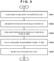
- step S501 the controller 13 controls the conveyance apparatus 14 so that the substrate chuck 4 will be placed on the hand 15 and the substrate chuck 4 will be subsequently mounted onto the substrate stage 5.
- step S502 the controller 13 measures, based on the detection result obtained by the detector 16, the position (rotational shift) of the substrate chuck 4 in the rotation direction ( ⁇ z direction). As shown in Fig. 2 , the plurality of marks 18 are formed on the substrate chuck 4.
- the controller 13 can obtain the position of the substrate chuck 4 in the rotation direction by using the detector 16 to detect the position of each mark 18 and calculating a difference between the detected position and the position of the mark 18 without the rotational shift.
- the controller 13 will adjust the position of the substrate stage 5 in the X direction and the Y direction to allow the detector 16 to detect the mark 18.
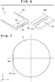
- Fig. 2 shows an example in which the plurality of marks 18 are formed on the substrate chuck 4
- a portion of the periphery of the substrate chuck 4 can be formed as a straight portion 182 (orientation flat) and this portion can be used as the mark as shown in Fig. 7 .
- the detector 16 will detect this straight portion 182. Letting a state in which the straight portion 182 is parallel to the Y direction be a state without a rotational shift, the rotational shift amount of the substrate chuck 4 can be calculated based a known length of the straight portion 182 and a shift amount ⁇ A of the straight portion 182 in the X direction.
- a back-side observation optical system (not shown) for observing the back surface side (suction surface side) of the substrate is arranged inside the substrate chuck 4
- the detector 16 will detect, via the back-side observation optical system in the substrate chuck 4, each alignment mark on the suction surface of a substrate placed on the substrate chuck 4. Since the rotational shift of the substrate chuck 4 will cause a relative positional shift between the back-side observation optical system and each alignment mark on the suction surface of the substrate, the field of view will become narrower during alignment mark detection. The rotational shift of the chuck may be calculated based on this shift amount of the field of view.
- step S503 the controller 13 controls the conveyance apparatus 14 to raise the substrate chuck 4 from the mounting surface of the substrate stage 5 by using the hand 15. This is performed to prevent friction between the substrate chuck 4 and the substrate stage 5 when the substrate chuck 4 is to be rotated in the following step S504.
- step S504 positional adjustment of the substrate chuck 4 in the rotation direction about the center axis is performed. More specifically, in step S504, the controller 13 rotates the hand 15 in the ⁇ z direction based on the measurement result of step S502. At this time, the substrate chuck 4 may be temporarily removed from the hand 15, and the substrate chuck 4 may be placed on the hand 15 again after the positional adjustment of the hand 15 has been completed. Also, the rotation driving operation may be performed manually by a human hand instead of being performed under automatic control by the controller 13.
- step S505 the conveyance apparatus 14 to place the substrate chuck 4 onto the substrate stage 5. If this operation is to be performed manually, a process for confirming whether the rotational shift of the substrate chuck 4 is within an allowable range may be performed by using the detector 16 after the substrate chuck 4 has been mounted onto the substrate stage 5.
- the hand 15 is arranged to be detachable from the main body 159.
- a rotation-adjusted chuck ⁇ is to be replaced with a chuck ⁇ different from the chuck ⁇
- a set formed by the chuck ⁇ and a rotation-adjusted rotating hand A may be replaced with a set formed by the chuck ⁇ and a rotating hand B. This will allow the processes of steps S502 to S505 to be omitted when the chuck ⁇ is to be mounted onto the substrate stage 5 again.
- a convex portion 191 which is formed in an arc shape of a circle centered about the vertical axis of the reference position 154 (see Fig. 2 ) between the two hand distal end portions 151, is formed on the back surface of the hand proximal end portion 152 of the hand 15.
- a concave portion that is shaped in the above-described arc shape of the circle and engages with the convex portion 191 is formed as the guiding portion 171 on the front surface of the main body 159. This kind of arrangement will allow the hand 15 to be pivoted accurately.
- This modification may also include a restricting portion that restricts the hand 15 from positionally shifting in the horizontal direction with respect to the main body 159 during the pivotal motion of the hand 15.
- the engaging portion 155 and the protrusion 158 similar to those shown in Figs. 3 and 4 , respectively, are shown in the example of Fig. 6 as well.
- the engaging protrusions 156 as shown in Fig. 3 can be provided on the respective placement surfaces of the two hand distal end portions 151.
- the engaging protrusions 156 are not shown in Fig. 6 since the placement surfaces of the two hand distal end portions 151 are located at the respective lower surfaces of the two hand distal end portions.
- a method of manufacturing an article according to the embodiment of the present invention is suitable for manufacturing an article such as a microdevice such as a semiconductor device or an element having a microstructure.
- the method of manufacturing an article according to the embodiment can include a step of forming a pattern of an original on a substrate by using the above-described substrate processing apparatus, and a step of processing the substrate on which the pattern has been formed in the preceding step.
- this article manufacturing method can include other well-known steps (oxidization, deposition, vapor deposition, doping, planarization, etching, resist removal, dicing, bonding, packaging, and the like).
- the method of manufacturing an article according to the embodiment is superior to a conventional method in at least one of the performance, quality, productivity, and production cost of an article.
- a conveyance apparatus for conveying a substrate chuck comprises a hand for supporting the substrate chuck, a main body for pivotally supporting the hand about a vertical axis and move in horizontal and vertical directions, and a guiding portion for guiding pivotal motion of the hand.
- the hand includes hand distal end portions and a hand proximal end portion supported by the main body, and an end surface of the hand proximal end portion facing the main body is formed in an arc shape of a circle centered about a vertical axis of a reference position between the hand distal end portions, and the guiding portion includes a guiding surface that has a shape corresponding to the end surface of the hand proximal end portion and can slidably contact the end surface.
Landscapes
- Engineering & Computer Science (AREA)
- Physics & Mathematics (AREA)
- General Physics & Mathematics (AREA)
- Power Engineering (AREA)
- Computer Hardware Design (AREA)
- Microelectronics & Electronic Packaging (AREA)
- Condensed Matter Physics & Semiconductors (AREA)
- Manufacturing & Machinery (AREA)
- Robotics (AREA)
- Container, Conveyance, Adherence, Positioning, Of Wafer (AREA)
- Exposure Of Semiconductors, Excluding Electron Or Ion Beam Exposure (AREA)
- Exposure And Positioning Against Photoresist Photosensitive Materials (AREA)
- Manipulator (AREA)
Applications Claiming Priority (1)
| Application Number | Priority Date | Filing Date | Title |
|---|---|---|---|
| JP2020111911A JP7579072B2 (ja) | 2020-06-29 | 2020-06-29 | 搬送装置、基板処理装置、および物品製造方法 |
Publications (1)
| Publication Number | Publication Date |
|---|---|
| EP3933507A1 true EP3933507A1 (en) | 2022-01-05 |
Family
ID=76137932
Family Applications (1)
| Application Number | Title | Priority Date | Filing Date |
|---|---|---|---|
| EP21175861.0A Pending EP3933507A1 (en) | 2020-06-29 | 2021-05-26 | Conveyance apparatus, substrate processing apparatus, and method of manufacturing article |
Country Status (4)
| Country | Link |
|---|---|
| US (1) | US11569119B2 (enExample) |
| EP (1) | EP3933507A1 (enExample) |
| JP (1) | JP7579072B2 (enExample) |
| CN (1) | CN113937042B (enExample) |
Families Citing this family (1)
| Publication number | Priority date | Publication date | Assignee | Title |
|---|---|---|---|---|
| US11468590B2 (en) * | 2018-04-24 | 2022-10-11 | Cyberoptics Corporation | Wireless substrate-like teaching sensor for semiconductor processing |
Citations (6)
| Publication number | Priority date | Publication date | Assignee | Title |
|---|---|---|---|---|
| JP2000021956A (ja) | 1998-07-02 | 2000-01-21 | Mecs Corp | ノッチ合わせ機 |
| WO2004077531A1 (de) * | 2003-02-25 | 2004-09-10 | Technische Universität München | Vorrichtung zum berührungsarmen greifen, halten und ausrichten von berührungsempfindlichen flachbauteilen |
| WO2014054034A2 (en) * | 2012-10-05 | 2014-04-10 | Koninklijke Philips N.V. | Rotary positioning device |
| JP5721453B2 (ja) | 2011-01-28 | 2015-05-20 | リンテック株式会社 | アライメント装置及びアライメント方法 |
| WO2015135782A1 (en) * | 2014-03-12 | 2015-09-17 | Asml Netherlands B.V. | Sensor system, substrate handling system and lithographic apparatus |
| US20170069517A1 (en) * | 2015-09-03 | 2017-03-09 | Kawasaki Jukogyo Kabushiki Kaisha | Substrate transfer device |
Family Cites Families (17)
| Publication number | Priority date | Publication date | Assignee | Title |
|---|---|---|---|---|
| US6516244B1 (en) * | 2000-08-25 | 2003-02-04 | Wafermasters, Inc. | Wafer alignment system and method |
| JP4014031B2 (ja) * | 2002-06-05 | 2007-11-28 | 東京エレクトロン株式会社 | 基板処理装置及び基板処理方法 |
| JP2004193344A (ja) * | 2002-12-11 | 2004-07-08 | Tokyo Electron Ltd | 基板搬送装置及び基板搬送方法 |
| US7654596B2 (en) * | 2003-06-27 | 2010-02-02 | Mattson Technology, Inc. | Endeffectors for handling semiconductor wafers |
| KR20060078016A (ko) * | 2004-12-30 | 2006-07-05 | 삼성전자주식회사 | 웨이퍼 에지 노광 장치 |
| US7706908B2 (en) * | 2005-02-22 | 2010-04-27 | Oc Oerlikon Balzers Ag | Method for positioning a wafer |
| JP2006351863A (ja) * | 2005-06-16 | 2006-12-28 | Nikon Corp | 物体搬送装置及び露光装置 |
| TWI638241B (zh) * | 2012-03-26 | 2018-10-11 | 日商尼康股份有限公司 | 基板處理裝置、處理裝置及元件製造方法 |
| JP6263017B2 (ja) * | 2013-12-16 | 2018-01-17 | 川崎重工業株式会社 | 基板位置合わせ装置及び基板位置合わせ装置の制御方法 |
| CN104449949A (zh) * | 2014-12-02 | 2015-03-25 | 湖南东博墨烯科技有限公司 | 一种石墨烯基纳米零价钴-铁-铜系润滑油及其制备方法 |
| JP6276317B2 (ja) * | 2016-03-31 | 2018-02-07 | 平田機工株式会社 | ハンドユニットおよび移載方法 |
| CN106590840B (zh) * | 2016-12-06 | 2019-10-11 | 重庆中领环保产业技术研究院有限公司 | 一种掺杂碳纳米类石墨烯润滑油添加剂及其制备方法 |
| KR102099110B1 (ko) * | 2017-10-12 | 2020-05-15 | 세메스 주식회사 | 기판 정렬 장치, 기판 처리 장치 및 기판 처리 방법 |
| JP7008573B2 (ja) * | 2018-05-16 | 2022-01-25 | 東京エレクトロン株式会社 | 搬送方法および搬送装置 |
| CN108822932B (zh) * | 2018-05-21 | 2021-07-23 | 上海利物盛企业集团有限公司 | 一种高速极压耐磨润滑油及其制备方法和应用 |
| US11335578B2 (en) * | 2020-02-13 | 2022-05-17 | Kawasaki Jukogyo Kabushiki Kaisha | Substrate transfer apparatus and method of measuring positional deviation of substrate |
| CN115011398A (zh) * | 2022-07-05 | 2022-09-06 | 上海中孚油品集团有限公司 | 一种石墨烯不锈钢管高速拉拔润滑油及其制备方法 |
-
2020
- 2020-06-29 JP JP2020111911A patent/JP7579072B2/ja active Active
-
2021
- 2021-05-26 EP EP21175861.0A patent/EP3933507A1/en active Pending
- 2021-06-04 US US17/338,836 patent/US11569119B2/en active Active
- 2021-06-25 CN CN202110709764.8A patent/CN113937042B/zh active Active
Patent Citations (6)
| Publication number | Priority date | Publication date | Assignee | Title |
|---|---|---|---|---|
| JP2000021956A (ja) | 1998-07-02 | 2000-01-21 | Mecs Corp | ノッチ合わせ機 |
| WO2004077531A1 (de) * | 2003-02-25 | 2004-09-10 | Technische Universität München | Vorrichtung zum berührungsarmen greifen, halten und ausrichten von berührungsempfindlichen flachbauteilen |
| JP5721453B2 (ja) | 2011-01-28 | 2015-05-20 | リンテック株式会社 | アライメント装置及びアライメント方法 |
| WO2014054034A2 (en) * | 2012-10-05 | 2014-04-10 | Koninklijke Philips N.V. | Rotary positioning device |
| WO2015135782A1 (en) * | 2014-03-12 | 2015-09-17 | Asml Netherlands B.V. | Sensor system, substrate handling system and lithographic apparatus |
| US20170069517A1 (en) * | 2015-09-03 | 2017-03-09 | Kawasaki Jukogyo Kabushiki Kaisha | Substrate transfer device |
Also Published As
| Publication number | Publication date |
|---|---|
| JP7579072B2 (ja) | 2024-11-07 |
| CN113937042B (zh) | 2025-05-23 |
| US20210407844A1 (en) | 2021-12-30 |
| US11569119B2 (en) | 2023-01-31 |
| CN113937042A (zh) | 2022-01-14 |
| JP2022011045A (ja) | 2022-01-17 |
Similar Documents
| Publication | Publication Date | Title |
|---|---|---|
| US5959721A (en) | Projection exposure apparatus and projection exposure method | |
| US5966201A (en) | Mark for position detection, and mark detecting method and apparatus | |
| EP1063186A1 (en) | Substrate transferring device and method | |
| US20090233195A1 (en) | Linewidth measuring method, image-forming-state detecting method, adjustment method, exposure method, and device manufacturing method | |
| JPH10163099A (ja) | 露光方法及び露光装置 | |
| JP6980562B2 (ja) | パターン形成装置、アライメントマークの検出方法及びパターン形成方法 | |
| JP2001274080A (ja) | 走査型投影露光装置及びその位置合わせ方法 | |
| US7990519B2 (en) | Exposure apparatus and device manufacturing method | |
| JP2001093808A (ja) | 露光方法及び露光装置 | |
| JP2004095653A (ja) | 露光装置 | |
| US11569119B2 (en) | Conveyance apparatus, substrate processing apparatus, and method of manufacturing article | |
| JP2004158610A (ja) | 露光装置および露光方法 | |
| JP2003156322A (ja) | 位置計測方法及び装置、位置決め方法、露光装置、並びにマイクロデバイスの製造方法 | |
| US20040025322A1 (en) | Waffle wafer chuck apparatus and method | |
| JP2000228347A (ja) | 位置決め方法及び露光装置 | |
| JP2003060000A (ja) | 基板搬送装置及び露光装置、並びにデバイス製造方法 | |
| JPH10189443A (ja) | 位置検出用マーク、マーク検出方法及びその装置並びに露光装置 | |
| JPH11219999A (ja) | 基板の受け渡し方法、及び該方法を使用する露光装置 | |
| JP2004235460A (ja) | 露光システム、走査型露光装置及び露光方法 | |
| JP2000077301A (ja) | 露光装置 | |
| JP4817700B2 (ja) | 露光装置及び方法、並びに、デバイス製造方法 | |
| JP2009206323A (ja) | 露光装置 | |
| US20240053686A1 (en) | Exposure apparatus, exposure method and article manufacturing method | |
| CN111123658A (zh) | 载置台装置、光刻装置及物品的制造方法 | |
| KR102817489B1 (ko) | 조명 광학계, 노광장치, 및 물품 제조방법 |
Legal Events
| Date | Code | Title | Description |
|---|---|---|---|
| PUAI | Public reference made under article 153(3) epc to a published international application that has entered the european phase |
Free format text: ORIGINAL CODE: 0009012 |
|
| STAA | Information on the status of an ep patent application or granted ep patent |
Free format text: STATUS: THE APPLICATION HAS BEEN PUBLISHED |
|
| AK | Designated contracting states |
Kind code of ref document: A1 Designated state(s): AL AT BE BG CH CY CZ DE DK EE ES FI FR GB GR HR HU IE IS IT LI LT LU LV MC MK MT NL NO PL PT RO RS SE SI SK SM TR |
|
| B565 | Issuance of search results under rule 164(2) epc |
Effective date: 20211111 |
|
| STAA | Information on the status of an ep patent application or granted ep patent |
Free format text: STATUS: REQUEST FOR EXAMINATION WAS MADE |
|
| 17P | Request for examination filed |
Effective date: 20220705 |
|
| RBV | Designated contracting states (corrected) |
Designated state(s): AL AT BE BG CH CY CZ DE DK EE ES FI FR GB GR HR HU IE IS IT LI LT LU LV MC MK MT NL NO PL PT RO RS SE SI SK SM TR |