EP3916934A1 - Laser module and electronic device - Google Patents
Laser module and electronic device Download PDFInfo
- Publication number
- EP3916934A1 EP3916934A1 EP20745019.8A EP20745019A EP3916934A1 EP 3916934 A1 EP3916934 A1 EP 3916934A1 EP 20745019 A EP20745019 A EP 20745019A EP 3916934 A1 EP3916934 A1 EP 3916934A1
- Authority
- EP
- European Patent Office
- Prior art keywords
- electrode
- side plate
- extension piece
- heat dissipation
- laser module
- Prior art date
- Legal status (The legal status is an assumption and is not a legal conclusion. Google has not performed a legal analysis and makes no representation as to the accuracy of the status listed.)
- Granted
Links
Images


Classifications
-
- H—ELECTRICITY
- H01—ELECTRIC ELEMENTS
- H01S—DEVICES USING THE PROCESS OF LIGHT AMPLIFICATION BY STIMULATED EMISSION OF RADIATION [LASER] TO AMPLIFY OR GENERATE LIGHT; DEVICES USING STIMULATED EMISSION OF ELECTROMAGNETIC RADIATION IN WAVE RANGES OTHER THAN OPTICAL
- H01S5/00—Semiconductor lasers
- H01S5/02—Structural details or components not essential to laser action
- H01S5/022—Mountings; Housings
- H01S5/02218—Material of the housings; Filling of the housings
-
- H—ELECTRICITY
- H01—ELECTRIC ELEMENTS
- H01S—DEVICES USING THE PROCESS OF LIGHT AMPLIFICATION BY STIMULATED EMISSION OF RADIATION [LASER] TO AMPLIFY OR GENERATE LIGHT; DEVICES USING STIMULATED EMISSION OF ELECTROMAGNETIC RADIATION IN WAVE RANGES OTHER THAN OPTICAL
- H01S5/00—Semiconductor lasers
- H01S5/02—Structural details or components not essential to laser action
- H01S5/022—Mountings; Housings
- H01S5/0225—Out-coupling of light
-
- H—ELECTRICITY
- H01—ELECTRIC ELEMENTS
- H01S—DEVICES USING THE PROCESS OF LIGHT AMPLIFICATION BY STIMULATED EMISSION OF RADIATION [LASER] TO AMPLIFY OR GENERATE LIGHT; DEVICES USING STIMULATED EMISSION OF ELECTROMAGNETIC RADIATION IN WAVE RANGES OTHER THAN OPTICAL
- H01S5/00—Semiconductor lasers
- H01S5/02—Structural details or components not essential to laser action
- H01S5/022—Mountings; Housings
- H01S5/0233—Mounting configuration of laser chips
- H01S5/02345—Wire-bonding
-
- H—ELECTRICITY
- H01—ELECTRIC ELEMENTS
- H01S—DEVICES USING THE PROCESS OF LIGHT AMPLIFICATION BY STIMULATED EMISSION OF RADIATION [LASER] TO AMPLIFY OR GENERATE LIGHT; DEVICES USING STIMULATED EMISSION OF ELECTROMAGNETIC RADIATION IN WAVE RANGES OTHER THAN OPTICAL
- H01S5/00—Semiconductor lasers
- H01S5/02—Structural details or components not essential to laser action
- H01S5/022—Mountings; Housings
- H01S5/0235—Method for mounting laser chips
-
- H—ELECTRICITY
- H01—ELECTRIC ELEMENTS
- H01S—DEVICES USING THE PROCESS OF LIGHT AMPLIFICATION BY STIMULATED EMISSION OF RADIATION [LASER] TO AMPLIFY OR GENERATE LIGHT; DEVICES USING STIMULATED EMISSION OF ELECTROMAGNETIC RADIATION IN WAVE RANGES OTHER THAN OPTICAL
- H01S5/00—Semiconductor lasers
- H01S5/02—Structural details or components not essential to laser action
- H01S5/024—Arrangements for thermal management
- H01S5/02469—Passive cooling, e.g. where heat is removed by the housing as a whole or by a heat pipe without any active cooling element like a TEC
-
- H—ELECTRICITY
- H01—ELECTRIC ELEMENTS
- H01S—DEVICES USING THE PROCESS OF LIGHT AMPLIFICATION BY STIMULATED EMISSION OF RADIATION [LASER] TO AMPLIFY OR GENERATE LIGHT; DEVICES USING STIMULATED EMISSION OF ELECTROMAGNETIC RADIATION IN WAVE RANGES OTHER THAN OPTICAL
- H01S5/00—Semiconductor lasers
- H01S5/02—Structural details or components not essential to laser action
- H01S5/024—Arrangements for thermal management
- H01S5/02476—Heat spreaders, i.e. improving heat flow between laser chip and heat dissipating elements
-
- H—ELECTRICITY
- H01—ELECTRIC ELEMENTS
- H01S—DEVICES USING THE PROCESS OF LIGHT AMPLIFICATION BY STIMULATED EMISSION OF RADIATION [LASER] TO AMPLIFY OR GENERATE LIGHT; DEVICES USING STIMULATED EMISSION OF ELECTROMAGNETIC RADIATION IN WAVE RANGES OTHER THAN OPTICAL
- H01S5/00—Semiconductor lasers
- H01S5/02—Structural details or components not essential to laser action
- H01S5/022—Mountings; Housings
- H01S5/02208—Mountings; Housings characterised by the shape of the housings
-
- H—ELECTRICITY
- H01—ELECTRIC ELEMENTS
- H01S—DEVICES USING THE PROCESS OF LIGHT AMPLIFICATION BY STIMULATED EMISSION OF RADIATION [LASER] TO AMPLIFY OR GENERATE LIGHT; DEVICES USING STIMULATED EMISSION OF ELECTROMAGNETIC RADIATION IN WAVE RANGES OTHER THAN OPTICAL
- H01S5/00—Semiconductor lasers
- H01S5/02—Structural details or components not essential to laser action
- H01S5/022—Mountings; Housings
- H01S5/0225—Out-coupling of light
- H01S5/02253—Out-coupling of light using lenses
-
- H—ELECTRICITY
- H01—ELECTRIC ELEMENTS
- H01S—DEVICES USING THE PROCESS OF LIGHT AMPLIFICATION BY STIMULATED EMISSION OF RADIATION [LASER] TO AMPLIFY OR GENERATE LIGHT; DEVICES USING STIMULATED EMISSION OF ELECTROMAGNETIC RADIATION IN WAVE RANGES OTHER THAN OPTICAL
- H01S5/00—Semiconductor lasers
- H01S5/02—Structural details or components not essential to laser action
- H01S5/022—Mountings; Housings
- H01S5/0225—Out-coupling of light
- H01S5/02257—Out-coupling of light using windows, e.g. specially adapted for back-reflecting light to a detector inside the housing
Definitions
- This disclosure relates to the field of laser device technologies, and in particular, to a laser module and an electronic device.
- a 3D recognition technology is widely used in fields such as face recognition for unlocking and payment.
- a laser module is an indispensable core component for 3D recognition, and is mainly used to emit ultra-short femtosecond pulses or project specific light patterns, so that a system obtains depth information.
- a laser chip plays a key role during working of the laser module.
- the laser chip is a semiconductor device sensitive to temperature. A higher temperature indicates a lower photoelectric conversion efficiency of the laser chip. The high temperature may easily damage a lattice structure of the laser chip to reduce a service life of the laser chip.
- laser chips mostly dissipate heat through circuit boards connected to the laser chips, resulting in low heat dissipation efficiency of the laser chips.
- Embodiments of this disclosure provide a laser module and an electronic device, so as to resolve a problem of low heat dissipation efficiency of a laser chip in a laser module in the related art.
- an embodiment of this disclosure provides a laser module, including:
- an embodiment of this disclosure further provides an electronic device, where the electronic device includes the laser module according to the first aspect.
- the heat dissipation structure abuts against the first electrode and the second electrode of the power supply structure, and therefore the first electrode and the second electrode can conduct heat generated by the laser chip, the first electrode, and the second electrode to the heat dissipation structure. Furthermore, the heat dissipation structure sleeved on the outer side of the packaging structure makes the heat dissipation structure have a larger heat dissipation area for heat dissipation, thereby improving heat dissipation efficiency of the laser module to ensure working performance and a service life of the laser chip. In addition, the heat dissipation structure sleeved on the outer side of the packaging structure can function to fasten and support the packaging structure.
- FIG. 1 is a sectional view of a laser module according to an embodiment of this disclosure
- FIG. 2 is a top view of the laser module in FIG. 1
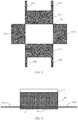
- FIG. 3 is a structural diagram of a heat dissipation body in the laser module provided in FIG. 1
- FIG. 4 is a structural diagram of a heat dissipation body that has not been installed in the laser module provided in FIG. 1
- FIG. 5 is a left side view of FIG. 4 .
- an embodiment of this disclosure provides a laser module, including an optical assembly 10, a laser chip 20, a power supply structure 30, a packaging structure 40, and a heat dissipation structure 50.
- the laser chip 20 is disposed on a side of the optical assembly 10, and the power supply structure 30 includes a first electrode 31 and a second electrode 32.
- the first electrode 31 and the second electrode 32 are both connected to the laser chip 20 for supplying power to the laser chip 20.
- An accommodating cavity is formed in the packaging structure 40 and the optical assembly 10 is at least partially received in the accommodating cavity.
- the heat dissipation structure 50 is sleeved on the outer side of the packaging structure 40, and the heat dissipation structure 50 abuts against the first electrode 31 and the second electrode 32.
- the heat dissipation structure 50 abuts against the first electrode 31 and the second electrode 32, and therefore the first electrode 31 and the second electrode 32 can conduct heat generated by the laser chip 20, the first electrode 31, and the second electrode 32 to the heat dissipation structure 50. Furthermore, the heat dissipation structure 50 sleeved on the outer side of the packaging structure 40 makes the heat dissipation structure 50 have a larger heat dissipation area for heat dissipation, thereby improving heat dissipation efficiency of the laser module to ensure working performance and a service life of the laser chip 20.
- the heat dissipation structure 50 sleeved on the outer side of the packaging structure 40 can function to fasten and support the packaging structure 40.
- the heat dissipation structure 50 may be a tubular structure that sleeves an outer surface of the packaging structure 40 to surround the packaging structure 40, thereby fastening the packaging structure 40.
- the heat dissipation structure 50 may be a material with relatively optimal thermal conductivity but no electrical conductivity, so as to ensure the heat dissipation performance of the heat dissipation structure 50 and further prevent the power supply structure 30 from leaking electricity through the heat dissipation structure 50, thereby ensuring use safety of the laser module.
- the power supply structure 30 may be disposed on a side of the laser chip 20 away from the optical assembly 10.
- the power supply structure 30 may be a circuit board, and the laser chip 20 may be attached to the circuit board, so that the laser chip 20 and the power supply structure 30 have a larger contact area, to improve heat transfer efficiency between the power supply structure 30 and the laser chip 20 and further help improve heat dissipation efficiency of the laser chip 20.
- the laser chip 20 and the power supply structure 30 may be located outside the packaging structure 40.
- the laser chip 20 and the power supply structure 30 may be located inside the packaging structure 40, so that the laser chip 20 and the power supply structure 30 can be fastened by the packaging structure 40, further ensuring overall stability of the laser module.
- the heat dissipation structure 50 includes a heat dissipation body 51 and a heat conductor 52, and the heat dissipation body 51 is sleeved on the outer side of the packaging structure 40.
- One side of the heat conductor 52 abuts against the heat dissipation body 51, and another side of the heat conductor 52 abuts against the first electrode 31 and the second electrode 32.
- the heat conductor 52 is disposed between the power supply structure 30 and the heat dissipation body 51.
- the heat conductor 52 may have a ring structure, with an inner wall of the heat conductor 52 abutting against the first electrode 31 and the second electrode 32, and an outer wall of the heat conductor 52 abutting against the heat dissipation body 51.
- the first electrode 31 and the second electrode 32 each have a larger contact area with the heat conductor 52, so that the heat conductor 52 can absorb more quickly the heat that is conducted to the first electrode 31 and the second electrode 32 from the first electrode 31, the second electrode 32, and the laser chip 20, thereby improving the heat dissipation efficiency of the laser module.
- the heat conductor 52 is made of an electrically non-conductive material, and the heat dissipation body 51 is made of a metal material.
- the heat conductor 52 made of the electrically non-conductive material does not have electrical conductivity, so as to further prevent the power supply structure 30 from leaking electricity through the heat conductor 52, thereby ensuring use safety of the laser module.
- the heat dissipation body 51 made of the metal material has better thermal conductivity, and the heat dissipation body 51 made of the metal material has a better electromagnetic shielding effect.
- the material of the heat dissipation body 51 may be copper, and copper has a relatively high thermal conductivity coefficient and features good stability and low costs, thereby reducing manufacturing costs of the laser module.
- the heat dissipation body 51 is sleeved on the outer side of the packaging structure 40, and as shown in FIG. 1 , the laser chip 20 is received in the accommodating cavity of the packaging structure 40. Therefore, the heat dissipation body 51 made of the metal material can reduce electromagnetic interference of the laser module to other components of the electronic device.
- the heat dissipation body 51 includes a substrate 511 and an extension piece 512.
- the substrate 511 is sleeved on the outer side of the packaging structure 40, and the substrate 511 includes a first end and a second end opposite to each other, where the first end abuts against the heat conductor 52, and the second end is connected to the extension piece 512.
- the extension piece 512 is located on a side of the optical assembly 10 away from the laser chip 20.
- the substrate 511 may be a tubular structure that is sleeved on the outer surface of the packaging structure 40.
- the substrate 511 of the tubular structure includes the first end and the second end opposite to and facing away from each other.
- the first end abuts against the heat conductor 52 to absorb the heat of the heat conductor 52.
- the second end is close to the optical assembly 10, and the extension piece 512 is disposed on the second end.
- the extension piece 512 is located on the side of the optical assembly 10 away from the laser chip 20, to fasten the optical assembly 10, thereby ensuring installation stability of the optical assembly 10.
- the substrate 511 includes a first side plate 5111, a second side plate 5112, a third side plate 5113, and a fourth side plate 5114 that are sequentially connected.
- a first through hole 513 is surrounded by the first side plate 5111, the second side plate 5112, the third side plate 5113, and the fourth side plate 5114.
- the packaging structure 40 is located in the first through hole 513, and the extension piece 512 is disposed on the first side plate 5111 and/or the third side plate 5113.
- the through hole is square, and the packaging structure 40 is also a square structure.
- the first side plate 5111, the second side plate 5112, the third side plate 5113, and the fourth side plate 5114 are sequentially connected to form the square-shaped substrate 511, and the substrate 511 may be an outer surface that covers the packaging structure 40, so that the substrate 511 has a larger surface area to increase the heat dissipation area of the heat dissipation body 51, thereby improving the heat dissipation efficiency of the laser module and better supporting and fastening the packaging structure 40.
- the extension piece 512 may be disposed on the first side plate 5111 or the third side plate 5113, or the extension piece 512 is disposed on the first side plate 5111 and the third side plate 5113 each.
- the extension piece 512 is disposed on the first side plate 5111, with the extension piece 512 connected to the third side plate 5113, so that the extension piece 512 is attached to the optical assembly 10, to press the optical assembly 10, thereby fastening the optical assembly 10.
- the extension piece 512 is disposed on the first side plate 5111, the second side plate 5112, the third side plate 5113, and the fourth side plate 5114 each, and the extension pieces 512 are attached to the side of the optical assembly 10 away from the laser chip 20.
- the extension piece 512 can function to fasten the optical assembly 10.
- a first extension piece 5121 and a second extension piece 5122 are disposed on the first side plate 5111, and a third extension piece 5123 and a fourth extension piece 5124 are disposed on the third side plate 5113.
- the first extension piece 5121 is connected to the third extension piece 5123 and the second side plate 5112.
- the third extension piece 5123 is connected to the second side plate 5112
- the second extension piece 5122 is connected to the fourth extension piece 5124 and the fourth side plate 5114
- the fourth extension piece 5124 is connected to the fourth side plate 5114.
- first side plate 5111, the second side plate 5112, the third side plate 5113, and the fourth side plate 5114 are welded to form a hollow quadrangular prism structure, and the packaging structure 40 and part of the optical assembly 10 are all received in the quadrangular prism structure.
- the first extension piece 5121 and the third extension piece 5123 are both welded to the top end of the second side plate 5112, and the second extension piece 5122 and the fourth extension piece 5124 are both welded to the top end of the fourth side plate 5114.
- a top view of the laser module is shown in FIG. 2 .
- the first extension piece 5121, the third extension piece 5123, the second extension piece 5122, and the fourth extension piece 5124 also press on the top of the optical assembly 10, to further fasten the optical assembly 10, preventing the optical assembly 10 from falling off and ensuring stability of the laser module.
- additional fixing parts are not required to fasten the optical assembly 10, thereby reducing hardware costs of the laser module.
- a second through hole is formed in the heat conductor 52, the first electrode 31 and the second electrode 32 are located in the second through hole, and the first electrode 31 and the second electrode 32 both abut against the inner wall of the heat conductor 52.
- the first electrode 31 may be a positive electrode
- the second electrode 32 may be a negative electrode, so as to supply power to the laser chip 20.
- the first electrode 31 and the second electrode 32 may have a plate-like structure, and the first electrode 31 and the second electrode 32 may be packaged in the packaging structure 40.
- the laser chip 20 is attached to the first electrode 31, so that the laser chip 20 and the first electrode 31 have a larger contact area. In this way, the heat generated by the laser chip 20 can be conducted faster to the first electrode 31, and then conducted to the heat conductor 52 through the first electrode 31.
- the optical assembly 10 includes an optical element 11 and a collimating element 12.
- the collimating element 12 is disposed on a side of the laser chip 20, and the collimating element 12 is received in the accommodating cavity.
- the optical element 11 is disposed on a side of the collimating element 12 away from the laser chip 20, and the extension piece 512 abuts against a side of the optical element 11 away from the collimating element 12. It can be understood that the laser light emitted by the laser chip 20 passes through the collimating element 12 and is then projected to the optical element 11 in the form of parallel light.
- the optical element 11 is used to project the parallel light in the form of scattered light, so that the laser light emitted by the laser chip 20 can have a larger coverage.
- a light divergence element 13 is disposed on a side of the optical element facing the collimating element.
- the light divergence element 13 is used to diverge the laser light emitted by the laser chip 20, so that the laser light emitted by the light divergence element 13 has a larger emission angle.
- the light divergent element 13 may be a micro galvanometer.
- a process flow for components of the laser module may be as follows: first attach the laser chip 20 to the first electrode 31, and connect the laser chip 20 and the second electrode 32 through a wire; dispose the heat conductor 52 on the outer side of the first electrode 31 and on the outer side of the second electrode 32; package the first electrode 31, the second electrode 32, the heat conductor 52, and the laser chip 20 by using a packaging material to form the packaging structure 40; mount the collimating element 12 on the side of the laser chip 20 away from the first electrode 31; mount the optical element 11 on the side of the collimating element 12 away from the laser chip 20; bend the substrate 511 and the extension piece 512, attach the substrate 511 to the outer wall of the packaging structure 40, and attach the extension piece 512 to the optical element 11; and then weld the substrate 511 and the extension piece 512.
- the laser module provided in this embodiment of this disclosure has a simpler process flow and lower costs.
- the heat generated by the laser chip 20 can be conducted to the heat conductor 52 through the power supply structure 30, and then conducted to the heat dissipation body 51 through the heat conductor 52.
- the heat dissipation body 51 sleeved on the outer side of the packaging structure 40 has a larger overall area, and therefore has a larger heat dissipation area for heat dissipation, improving the heat dissipation efficiency of the laser module and ensuring the working performance and service life of the laser chip 20.
- the higher heat dissipation efficiency is also good for development of high-power laser modules to apply 3D recognition to long-distance photographing.
- An embodiment of this disclosure further provides an electronic device.
- the electronic device includes the laser module in the embodiment described in FIG. 1 to FIG. 5 , and has all technical features of the laser module in the foregoing embodiment, with the same technical effects achieved. Details are not be repeated herein.
- the electronic device may include at least one of a mobile phone, a tablet computer, an e-book reader, an MP3 player, an MP4 player, a digital camera, a laptop computer, an in-vehicle computer, a desktop computer, a set-top box, a smart TV, a wearable device, and a smart home appliance.
Landscapes
- Physics & Mathematics (AREA)
- Condensed Matter Physics & Semiconductors (AREA)
- General Physics & Mathematics (AREA)
- Electromagnetism (AREA)
- Optics & Photonics (AREA)
- Semiconductor Lasers (AREA)
Abstract
Description
- This application claims priority to
Chinese Patent Application No. 201910073154.6 - This disclosure relates to the field of laser device technologies, and in particular, to a laser module and an electronic device.
- A 3D recognition technology is widely used in fields such as face recognition for unlocking and payment. A laser module is an indispensable core component for 3D recognition, and is mainly used to emit ultra-short femtosecond pulses or project specific light patterns, so that a system obtains depth information. As one of the most important components in the laser module, a laser chip plays a key role during working of the laser module.
- The laser chip is a semiconductor device sensitive to temperature. A higher temperature indicates a lower photoelectric conversion efficiency of the laser chip. The high temperature may easily damage a lattice structure of the laser chip to reduce a service life of the laser chip. However, for laser modules in the related art, laser chips mostly dissipate heat through circuit boards connected to the laser chips, resulting in low heat dissipation efficiency of the laser chips.
- Embodiments of this disclosure provide a laser module and an electronic device, so as to resolve a problem of low heat dissipation efficiency of a laser chip in a laser module in the related art.
- In order to resolve the foregoing technical problem, this disclosure is implemented as follows:
- According to a first aspect, an embodiment of this disclosure provides a laser module, including:
- an optical assembly;
- a laser chip, disposed on a side of the optical assembly;
- a power supply structure, including a first electrode and a second electrode, where the first electrode and the second electrode are both connected to the laser chip;
- a packaging structure in which an accommodating cavity is formed, where the optical assembly is at least partially received in the accommodating cavity; and
- a heat dissipation structure, sleeved on an outer side of the packaging structure, where the heat dissipation structure abuts against the first electrode and the second electrode.
- According to a second aspect, an embodiment of this disclosure further provides an electronic device, where the electronic device includes the laser module according to the first aspect.
- According to the technical solutions provided in the embodiments of this disclosure, the heat dissipation structure abuts against the first electrode and the second electrode of the power supply structure, and therefore the first electrode and the second electrode can conduct heat generated by the laser chip, the first electrode, and the second electrode to the heat dissipation structure. Furthermore, the heat dissipation structure sleeved on the outer side of the packaging structure makes the heat dissipation structure have a larger heat dissipation area for heat dissipation, thereby improving heat dissipation efficiency of the laser module to ensure working performance and a service life of the laser chip. In addition, the heat dissipation structure sleeved on the outer side of the packaging structure can function to fasten and support the packaging structure.
- To describe the technical solutions in the embodiments of this disclosure more clearly, the following briefly introduces the accompanying drawings required for describing the embodiments of this disclosure. Apparently, the accompanying drawings in the following description show merely some embodiments of this disclosure, and a person of ordinary skill in the art may still derive other drawings from these accompanying drawings without creative efforts.
-
FIG. 1 is a sectional view of a laser module according to an embodiment of this disclosure; -
FIG. 2 is a top view of the laser module inFIG. 1 ; -
FIG. 3 is a structural diagram of a heat dissipation body in the laser module provided inFIG. 1 ; -
FIG. 4 is a structural diagram of a heat dissipation body that has not been installed in the laser module provided inFIG. 1 ; and -
FIG. 5 is a left side view ofFIG. 4 . - The following clearly and completely describes the technical solutions in the embodiments of this disclosure with reference to the accompanying drawings in the embodiments of this disclosure. Apparently, the described embodiments are some but not all of the embodiments of this disclosure. All other embodiments obtained by a person of ordinary skill in the art based on the embodiments of this disclosure without creative efforts shall fall within the protection scope of this disclosure.
- Referring to
FIG. 1 to FIG. 5 ,FIG. 1 is a sectional view of a laser module according to an embodiment of this disclosure;FIG. 2 is a top view of the laser module inFIG. 1 ;FIG. 3 is a structural diagram of a heat dissipation body in the laser module provided inFIG. 1 ;FIG. 4 is a structural diagram of a heat dissipation body that has not been installed in the laser module provided inFIG. 1 ; andFIG. 5 is a left side view ofFIG. 4 . - Specifically referring to
FIG. 1 , an embodiment of this disclosure provides a laser module, including anoptical assembly 10, alaser chip 20, apower supply structure 30, apackaging structure 40, and aheat dissipation structure 50. Thelaser chip 20 is disposed on a side of theoptical assembly 10, and thepower supply structure 30 includes afirst electrode 31 and asecond electrode 32. Thefirst electrode 31 and thesecond electrode 32 are both connected to thelaser chip 20 for supplying power to thelaser chip 20. An accommodating cavity is formed in thepackaging structure 40 and theoptical assembly 10 is at least partially received in the accommodating cavity. Theheat dissipation structure 50 is sleeved on the outer side of thepackaging structure 40, and theheat dissipation structure 50 abuts against thefirst electrode 31 and thesecond electrode 32. - According to the technical solutions provided in the embodiments of this disclosure, the
heat dissipation structure 50 abuts against thefirst electrode 31 and thesecond electrode 32, and therefore thefirst electrode 31 and thesecond electrode 32 can conduct heat generated by thelaser chip 20, thefirst electrode 31, and thesecond electrode 32 to theheat dissipation structure 50. Furthermore, theheat dissipation structure 50 sleeved on the outer side of thepackaging structure 40 makes theheat dissipation structure 50 have a larger heat dissipation area for heat dissipation, thereby improving heat dissipation efficiency of the laser module to ensure working performance and a service life of thelaser chip 20. - In addition, the
heat dissipation structure 50 sleeved on the outer side of thepackaging structure 40 can function to fasten and support thepackaging structure 40. For example, in a case that thepackaging structure 40 is a columnar structure, theheat dissipation structure 50 may be a tubular structure that sleeves an outer surface of thepackaging structure 40 to surround thepackaging structure 40, thereby fastening thepackaging structure 40. - The
heat dissipation structure 50 may be a material with relatively optimal thermal conductivity but no electrical conductivity, so as to ensure the heat dissipation performance of theheat dissipation structure 50 and further prevent thepower supply structure 30 from leaking electricity through theheat dissipation structure 50, thereby ensuring use safety of the laser module. - Optionally, the
power supply structure 30 may be disposed on a side of thelaser chip 20 away from theoptical assembly 10. For example, thepower supply structure 30 may be a circuit board, and thelaser chip 20 may be attached to the circuit board, so that thelaser chip 20 and thepower supply structure 30 have a larger contact area, to improve heat transfer efficiency between thepower supply structure 30 and thelaser chip 20 and further help improve heat dissipation efficiency of thelaser chip 20. - The
laser chip 20 and thepower supply structure 30 may be located outside thepackaging structure 40. Alternatively, as shown inFIG. 1 , thelaser chip 20 and thepower supply structure 30 may be located inside thepackaging structure 40, so that thelaser chip 20 and thepower supply structure 30 can be fastened by thepackaging structure 40, further ensuring overall stability of the laser module. - In an optional implementation, the
heat dissipation structure 50 includes aheat dissipation body 51 and aheat conductor 52, and theheat dissipation body 51 is sleeved on the outer side of thepackaging structure 40. One side of theheat conductor 52 abuts against theheat dissipation body 51, and another side of theheat conductor 52 abuts against thefirst electrode 31 and thesecond electrode 32. In other words, theheat conductor 52 is disposed between thepower supply structure 30 and theheat dissipation body 51. For example, theheat conductor 52 may have a ring structure, with an inner wall of theheat conductor 52 abutting against thefirst electrode 31 and thesecond electrode 32, and an outer wall of theheat conductor 52 abutting against theheat dissipation body 51. In this case, thefirst electrode 31 and thesecond electrode 32 each have a larger contact area with theheat conductor 52, so that theheat conductor 52 can absorb more quickly the heat that is conducted to thefirst electrode 31 and thesecond electrode 32 from thefirst electrode 31, thesecond electrode 32, and thelaser chip 20, thereby improving the heat dissipation efficiency of the laser module. - The
heat conductor 52 is made of an electrically non-conductive material, and theheat dissipation body 51 is made of a metal material. Theheat conductor 52 made of the electrically non-conductive material does not have electrical conductivity, so as to further prevent thepower supply structure 30 from leaking electricity through theheat conductor 52, thereby ensuring use safety of the laser module. - The
heat dissipation body 51 made of the metal material has better thermal conductivity, and theheat dissipation body 51 made of the metal material has a better electromagnetic shielding effect. For example, the material of theheat dissipation body 51 may be copper, and copper has a relatively high thermal conductivity coefficient and features good stability and low costs, thereby reducing manufacturing costs of the laser module. - In addition, the
heat dissipation body 51 is sleeved on the outer side of thepackaging structure 40, and as shown inFIG. 1 , thelaser chip 20 is received in the accommodating cavity of thepackaging structure 40. Therefore, theheat dissipation body 51 made of the metal material can reduce electromagnetic interference of the laser module to other components of the electronic device. - Optionally, the
heat dissipation body 51 includes asubstrate 511 and anextension piece 512. Thesubstrate 511 is sleeved on the outer side of thepackaging structure 40, and thesubstrate 511 includes a first end and a second end opposite to each other, where the first end abuts against theheat conductor 52, and the second end is connected to theextension piece 512. Theextension piece 512 is located on a side of theoptical assembly 10 away from thelaser chip 20. - For example, when the
packaging structure 40 is a hollow columnar structure, and thesubstrate 511 may be a tubular structure that is sleeved on the outer surface of thepackaging structure 40. Thesubstrate 511 of the tubular structure includes the first end and the second end opposite to and facing away from each other. The first end abuts against theheat conductor 52 to absorb the heat of theheat conductor 52. The second end is close to theoptical assembly 10, and theextension piece 512 is disposed on the second end. Theextension piece 512 is located on the side of theoptical assembly 10 away from thelaser chip 20, to fasten theoptical assembly 10, thereby ensuring installation stability of theoptical assembly 10. - Referring to
FIG. 3 to FIG. 5 , in a specific implementation, thesubstrate 511 includes afirst side plate 5111, asecond side plate 5112, athird side plate 5113, and afourth side plate 5114 that are sequentially connected. A first throughhole 513 is surrounded by thefirst side plate 5111, thesecond side plate 5112, thethird side plate 5113, and thefourth side plate 5114. Thepackaging structure 40 is located in the first throughhole 513, and theextension piece 512 is disposed on thefirst side plate 5111 and/or thethird side plate 5113. The through hole is square, and thepackaging structure 40 is also a square structure. Thefirst side plate 5111, thesecond side plate 5112, thethird side plate 5113, and thefourth side plate 5114 are sequentially connected to form the square-shapedsubstrate 511, and thesubstrate 511 may be an outer surface that covers thepackaging structure 40, so that thesubstrate 511 has a larger surface area to increase the heat dissipation area of theheat dissipation body 51, thereby improving the heat dissipation efficiency of the laser module and better supporting and fastening thepackaging structure 40. - The
extension piece 512 may be disposed on thefirst side plate 5111 or thethird side plate 5113, or theextension piece 512 is disposed on thefirst side plate 5111 and thethird side plate 5113 each. For example, theextension piece 512 is disposed on thefirst side plate 5111, with theextension piece 512 connected to thethird side plate 5113, so that theextension piece 512 is attached to theoptical assembly 10, to press theoptical assembly 10, thereby fastening theoptical assembly 10. - Alternatively, the
extension piece 512 is disposed on thefirst side plate 5111, thesecond side plate 5112, thethird side plate 5113, and thefourth side plate 5114 each, and theextension pieces 512 are attached to the side of theoptical assembly 10 away from thelaser chip 20. In other words, theextension piece 512 can function to fasten theoptical assembly 10. - Specifically, referring to
FIG. 2 andFIG. 3 , afirst extension piece 5121 and asecond extension piece 5122 are disposed on thefirst side plate 5111, and athird extension piece 5123 and afourth extension piece 5124 are disposed on thethird side plate 5113. Thefirst extension piece 5121 is connected to thethird extension piece 5123 and thesecond side plate 5112. Thethird extension piece 5123 is connected to thesecond side plate 5112, thesecond extension piece 5122 is connected to thefourth extension piece 5124 and thefourth side plate 5114, and thefourth extension piece 5124 is connected to thefourth side plate 5114. - In this embodiment, the
first side plate 5111, thesecond side plate 5112, thethird side plate 5113, and thefourth side plate 5114 are welded to form a hollow quadrangular prism structure, and thepackaging structure 40 and part of theoptical assembly 10 are all received in the quadrangular prism structure. Thefirst extension piece 5121 and thethird extension piece 5123 are both welded to the top end of thesecond side plate 5112, and thesecond extension piece 5122 and thefourth extension piece 5124 are both welded to the top end of thefourth side plate 5114. A top view of the laser module is shown inFIG. 2 . In this way, thefirst extension piece 5121, thethird extension piece 5123, thesecond extension piece 5122, and thefourth extension piece 5124 also press on the top of theoptical assembly 10, to further fasten theoptical assembly 10, preventing theoptical assembly 10 from falling off and ensuring stability of the laser module. In addition, with such disposition, additional fixing parts are not required to fasten theoptical assembly 10, thereby reducing hardware costs of the laser module. - Referring to
FIG. 1 again, a second through hole is formed in theheat conductor 52, thefirst electrode 31 and thesecond electrode 32 are located in the second through hole, and thefirst electrode 31 and thesecond electrode 32 both abut against the inner wall of theheat conductor 52. Thefirst electrode 31 may be a positive electrode, and thesecond electrode 32 may be a negative electrode, so as to supply power to thelaser chip 20. Thefirst electrode 31 and thesecond electrode 32 may have a plate-like structure, and thefirst electrode 31 and thesecond electrode 32 may be packaged in thepackaging structure 40. - Optionally, the
laser chip 20 is attached to thefirst electrode 31, so that thelaser chip 20 and thefirst electrode 31 have a larger contact area. In this way, the heat generated by thelaser chip 20 can be conducted faster to thefirst electrode 31, and then conducted to theheat conductor 52 through thefirst electrode 31. - Optionally, the
optical assembly 10 includes anoptical element 11 and acollimating element 12. Thecollimating element 12 is disposed on a side of thelaser chip 20, and thecollimating element 12 is received in the accommodating cavity. Theoptical element 11 is disposed on a side of thecollimating element 12 away from thelaser chip 20, and theextension piece 512 abuts against a side of theoptical element 11 away from thecollimating element 12. It can be understood that the laser light emitted by thelaser chip 20 passes through thecollimating element 12 and is then projected to theoptical element 11 in the form of parallel light. Theoptical element 11 is used to project the parallel light in the form of scattered light, so that the laser light emitted by thelaser chip 20 can have a larger coverage. - In addition, a
light divergence element 13 is disposed on a side of the optical element facing the collimating element. Thelight divergence element 13 is used to diverge the laser light emitted by thelaser chip 20, so that the laser light emitted by thelight divergence element 13 has a larger emission angle. Optionally, the lightdivergent element 13 may be a micro galvanometer. - In this embodiment, a process flow for components of the laser module may be as follows: first attach the
laser chip 20 to thefirst electrode 31, and connect thelaser chip 20 and thesecond electrode 32 through a wire; dispose theheat conductor 52 on the outer side of thefirst electrode 31 and on the outer side of thesecond electrode 32; package thefirst electrode 31, thesecond electrode 32, theheat conductor 52, and thelaser chip 20 by using a packaging material to form thepackaging structure 40; mount thecollimating element 12 on the side of thelaser chip 20 away from thefirst electrode 31; mount theoptical element 11 on the side of thecollimating element 12 away from thelaser chip 20; bend thesubstrate 511 and theextension piece 512, attach thesubstrate 511 to the outer wall of thepackaging structure 40, and attach theextension piece 512 to theoptical element 11; and then weld thesubstrate 511 and theextension piece 512. The laser module provided in this embodiment of this disclosure has a simpler process flow and lower costs. - According to the technical solution provided in this embodiment of this disclosure, the heat generated by the
laser chip 20 can be conducted to theheat conductor 52 through thepower supply structure 30, and then conducted to theheat dissipation body 51 through theheat conductor 52. Theheat dissipation body 51 sleeved on the outer side of thepackaging structure 40 has a larger overall area, and therefore has a larger heat dissipation area for heat dissipation, improving the heat dissipation efficiency of the laser module and ensuring the working performance and service life of thelaser chip 20. Furthermore, the higher heat dissipation efficiency is also good for development of high-power laser modules to apply 3D recognition to long-distance photographing. - An embodiment of this disclosure further provides an electronic device. The electronic device includes the laser module in the embodiment described in
FIG. 1 to FIG. 5 , and has all technical features of the laser module in the foregoing embodiment, with the same technical effects achieved. Details are not be repeated herein. - The electronic device may include at least one of a mobile phone, a tablet computer, an e-book reader, an MP3 player, an MP4 player, a digital camera, a laptop computer, an in-vehicle computer, a desktop computer, a set-top box, a smart TV, a wearable device, and a smart home appliance.
- The foregoing descriptions are merely specific implementations of this disclosure, but are not intended to limit the protection scope of this disclosure. Any variation or replacement readily figured out by a person skilled in the art within the technical scope disclosed in this disclosure shall fall within the protection scope of this disclosure. Therefore, the protection scope of this disclosure shall be subject to the protection scope of the claims.
Claims (8)
- A laser module, comprising:an optical assembly;a laser chip, disposed on a side of the optical assembly;a power supply structure, comprising a first electrode and a second electrode, wherein the first electrode and the second electrode are both connected to the laser chip;a packaging structure in which an accommodating cavity is formed, wherein the optical assembly is at least partially received in the accommodating cavity; anda heat dissipation structure, sleeved on an outer side of the packaging structure, wherein the heat dissipation structure abuts against the first electrode and the second electrode;the heat dissipation structure comprises a heat dissipation body and a heat conductor, wherein the heat dissipation body is sleeved on the outer side of the packaging structure, one side of the heat conductor abuts against the heat dissipation body, and another side of the heat conductor abuts against the first electrode and the second electrode; andthe heat dissipation body comprises a substrate and an extension piece, wherein the substrate is sleeved on the outer side of the packaging structure, the substrate comprises a first end and a second end opposite to and facing away from each other, the first end abuts against the heat conductor, the second end is connected to the extension piece, and the extension piece is located on a side of the optical assembly away from the laser chip.
- The laser module according to claim 1, wherein the substrate comprises a first side plate, a second side plate, a third side plate, and a fourth side plate that are sequentially connected; a first through hole is surrounded by the first side plate, the second side plate, the third side plate, and the fourth side plate; the packaging structure is located in the first through hole; and the extension piece is disposed on the first side plate and/or the third side plate.
- The laser module according to claim 2, wherein a first extension piece and a second extension piece are disposed on the first side plate; a third extension piece and a fourth extension piece are disposed on the third side plate; the first extension piece is connected to the third extension piece and the second side plate; the third extension piece is connected to the second side plate; the second extension piece is connected to the fourth extension piece and the fourth side plate; and the fourth extension piece is connected to the fourth side plate.
- The laser module according to claim 2, wherein a second through hole is formed in the heat conductor; the first electrode and the second electrode are located in the second through hole; and the first electrode and the second electrode both abut against an inner wall of the heat conductor.
- The laser module according to claim 1, wherein the optical assembly comprises an optical element and a collimating element; the collimating element is disposed on a side of the laser chip, and the collimating element is received in the accommodating cavity; the optical element is disposed on a side of the collimating element away from the laser chip; and the extension piece abuts against a side of the optical element away from the collimating element.
- The laser module according to claim 5, wherein a light divergence element is disposed on a side of the optical element facing the collimating element.
- The laser module according to claim 1, wherein the heat conductor is made of an electrically non-conductive material, and the heat dissipation body is made of a metal material.
- An electronic device, comprising the laser module according to any one of claims 1 to 7.
Applications Claiming Priority (2)
| Application Number | Priority Date | Filing Date | Title |
|---|---|---|---|
| CN201910073154.6A CN109586165B (en) | 2019-01-25 | 2019-01-25 | Laser module and electronic equipment |
| PCT/CN2020/071689 WO2020151515A1 (en) | 2019-01-25 | 2020-01-13 | Laser module and electronic device |
Publications (3)
| Publication Number | Publication Date |
|---|---|
| EP3916934A1 true EP3916934A1 (en) | 2021-12-01 |
| EP3916934A4 EP3916934A4 (en) | 2022-03-23 |
| EP3916934B1 EP3916934B1 (en) | 2024-09-18 |
Family
ID=65917413
Family Applications (1)
| Application Number | Title | Priority Date | Filing Date |
|---|---|---|---|
| EP20745019.8A Active EP3916934B1 (en) | 2019-01-25 | 2020-01-13 | Laser module and electronic device |
Country Status (7)
| Country | Link |
|---|---|
| US (1) | US12015241B2 (en) |
| EP (1) | EP3916934B1 (en) |
| JP (1) | JP7208407B2 (en) |
| KR (1) | KR102507604B1 (en) |
| CN (1) | CN109586165B (en) |
| ES (1) | ES2994073T3 (en) |
| WO (1) | WO2020151515A1 (en) |
Families Citing this family (2)
| Publication number | Priority date | Publication date | Assignee | Title |
|---|---|---|---|---|
| CN109586165B (en) * | 2019-01-25 | 2020-04-07 | 维沃移动通信有限公司 | Laser module and electronic equipment |
| CN110190503A (en) | 2019-04-23 | 2019-08-30 | 维沃移动通信有限公司 | Fixing seat, laser projection mould group and electronic equipment |
Family Cites Families (23)
| Publication number | Priority date | Publication date | Assignee | Title |
|---|---|---|---|---|
| JPS55132088A (en) * | 1979-03-30 | 1980-10-14 | Canon Inc | Semiconductor laser device |
| US4918702A (en) * | 1987-12-02 | 1990-04-17 | Canon Kabushiki Kaisha | Laser unit |
| JP2560135B2 (en) * | 1990-06-14 | 1996-12-04 | ローム株式会社 | Method for filling transparent resin in semiconductor laser device |
| JP2560136B2 (en) * | 1990-06-14 | 1996-12-04 | ローム株式会社 | Semiconductor laser device |
| EP1282206A1 (en) * | 2001-07-30 | 2003-02-05 | Agilent Technologies, Inc. (a Delaware corporation) | Method and apparatus for cooling electronic or optoelectronic devices |
| JP3972814B2 (en) | 2002-12-26 | 2007-09-05 | ソニー株式会社 | Semiconductor integrated device |
| US7492798B2 (en) * | 2005-12-20 | 2009-02-17 | Finisar Corporation | Modular transistor outline can with internal components |
| JP5106094B2 (en) * | 2007-02-22 | 2012-12-26 | シャープ株式会社 | Surface mount type light emitting diode and method for manufacturing the same |
| KR20090017246A (en) * | 2007-08-14 | 2009-02-18 | 김정수 | Laser Diode Package with Heat Dissipation |
| US7855394B2 (en) * | 2009-06-18 | 2010-12-21 | Bridgelux, Inc. | LED array package covered with a highly thermal conductive plate |
| US8811439B2 (en) * | 2009-11-23 | 2014-08-19 | Seminex Corporation | Semiconductor laser assembly and packaging system |
| US8482924B2 (en) * | 2010-10-11 | 2013-07-09 | Richard Redpath | Heat spreader facet plane apparatus |
| DE102011116534B4 (en) * | 2011-10-20 | 2022-06-23 | OSRAM Opto Semiconductors Gesellschaft mit beschränkter Haftung | Radiation-emitting component |
| CN104303380A (en) * | 2012-05-01 | 2015-01-21 | 三菱电机株式会社 | Semiconductor package |
| JP6135032B2 (en) * | 2013-02-19 | 2017-05-31 | スタンレー電気株式会社 | Light emitting device, vehicle lamp, and stress relief part molding method |
| US9625671B2 (en) * | 2013-10-23 | 2017-04-18 | Lasermax, Inc. | Laser module and system |
| CN107454985B (en) * | 2015-03-30 | 2020-08-21 | 亮锐控股有限公司 | Peripheral Heat Dissipation Arrangement for High Brightness Lighting Device |
| JP6296024B2 (en) | 2015-08-28 | 2018-03-20 | 日亜化学工業株式会社 | Semiconductor laser device |
| JP6319257B2 (en) * | 2015-09-30 | 2018-05-09 | ウシオ電機株式会社 | Semiconductor laser device |
| JPWO2018173913A1 (en) * | 2017-03-21 | 2019-06-27 | 日本特殊陶業株式会社 | Light emitting device |
| JP6881248B2 (en) * | 2017-11-14 | 2021-06-02 | 日亜化学工業株式会社 | Optical member holding device, manufacturing method of optical member holding device and semiconductor laser device |
| JP7037043B2 (en) * | 2017-12-25 | 2022-03-16 | 日亜化学工業株式会社 | Abnormality detection method of light emitting device and light emitting device |
| CN109586165B (en) * | 2019-01-25 | 2020-04-07 | 维沃移动通信有限公司 | Laser module and electronic equipment |
-
2019
- 2019-01-25 CN CN201910073154.6A patent/CN109586165B/en active Active
-
2020
- 2020-01-13 WO PCT/CN2020/071689 patent/WO2020151515A1/en not_active Ceased
- 2020-01-13 EP EP20745019.8A patent/EP3916934B1/en active Active
- 2020-01-13 JP JP2021543259A patent/JP7208407B2/en active Active
- 2020-01-13 ES ES20745019T patent/ES2994073T3/en active Active
- 2020-01-13 KR KR1020217026756A patent/KR102507604B1/en active Active
-
2021
- 2021-07-21 US US17/381,536 patent/US12015241B2/en active Active
Also Published As
| Publication number | Publication date |
|---|---|
| CN109586165A (en) | 2019-04-05 |
| US12015241B2 (en) | 2024-06-18 |
| KR102507604B1 (en) | 2023-03-09 |
| EP3916934B1 (en) | 2024-09-18 |
| CN109586165B (en) | 2020-04-07 |
| WO2020151515A1 (en) | 2020-07-30 |
| KR20210116627A (en) | 2021-09-27 |
| JP2022520020A (en) | 2022-03-28 |
| ES2994073T3 (en) | 2025-01-16 |
| US20210351565A1 (en) | 2021-11-11 |
| EP3916934A4 (en) | 2022-03-23 |
| JP7208407B2 (en) | 2023-01-18 |
Similar Documents
| Publication | Publication Date | Title |
|---|---|---|
| EP3200226B1 (en) | Heat dissipation shielding structure and communication product | |
| US20170354057A1 (en) | Junction Box Thermal Management | |
| TWI475271B (en) | Intergrated sealed opto-electronic device | |
| US12015241B2 (en) | Laser module and electronic device | |
| US20150201530A1 (en) | Heat Spreading Packaging Apparatus | |
| EP3264870B1 (en) | Optical module | |
| TW201500789A (en) | Opto-electronic device assembly | |
| EP4081006B1 (en) | Heat dissipation device, circuit board assembly, and electronic apparatus | |
| US20100084180A1 (en) | Electronic device with a shielding member | |
| TWI495423B (en) | Thermal module and electronic device using the same | |
| US6707675B1 (en) | EMI containment device and method | |
| WO2023098503A1 (en) | Shielding structure, package body, board-level architecture, radiator, and electronic device | |
| CN110636701A (en) | Circuit board assembly and electronic equipment | |
| CN202121492U (en) | Power source and power source casing thereof | |
| CN221057156U (en) | Nuclear power plant radiation protection device | |
| CN105578706B (en) | circuit board assembly | |
| CN205611067U (en) | Electron device's installation device and subrack | |
| JP5072522B2 (en) | Connection structure | |
| US10130010B2 (en) | Internal heat-dissipation terminal | |
| KR20220025560A (en) | Printed Circuit Board module and Electronic device having the same | |
| CN204595282U (en) | A kind of optical transceiver module | |
| US20150001693A1 (en) | Leadframe pocket | |
| JP3162593U (en) | Heat dissipation device | |
| CN209979847U (en) | A laser transmitter, camera device and electronic device | |
| CN213151722U (en) | PCBA with wireless power supply module |
Legal Events
| Date | Code | Title | Description |
|---|---|---|---|
| STAA | Information on the status of an ep patent application or granted ep patent |
Free format text: STATUS: THE INTERNATIONAL PUBLICATION HAS BEEN MADE |
|
| PUAI | Public reference made under article 153(3) epc to a published international application that has entered the european phase |
Free format text: ORIGINAL CODE: 0009012 |
|
| STAA | Information on the status of an ep patent application or granted ep patent |
Free format text: STATUS: REQUEST FOR EXAMINATION WAS MADE |
|
| 17P | Request for examination filed |
Effective date: 20210823 |
|
| AK | Designated contracting states |
Kind code of ref document: A1 Designated state(s): AL AT BE BG CH CY CZ DE DK EE ES FI FR GB GR HR HU IE IS IT LI LT LU LV MC MK MT NL NO PL PT RO RS SE SI SK SM TR |
|
| A4 | Supplementary search report drawn up and despatched |
Effective date: 20220223 |
|
| RIC1 | Information provided on ipc code assigned before grant |
Ipc: H01S 5/022 20210101ALI20220217BHEP Ipc: H01S 5/024 20060101AFI20220217BHEP |
|
| DAV | Request for validation of the european patent (deleted) | ||
| DAX | Request for extension of the european patent (deleted) | ||
| GRAP | Despatch of communication of intention to grant a patent |
Free format text: ORIGINAL CODE: EPIDOSNIGR1 |
|
| GRAP | Despatch of communication of intention to grant a patent |
Free format text: ORIGINAL CODE: EPIDOSNIGR1 |
|
| STAA | Information on the status of an ep patent application or granted ep patent |
Free format text: STATUS: GRANT OF PATENT IS INTENDED |
|
| INTG | Intention to grant announced |
Effective date: 20240614 |
|
| GRAS | Grant fee paid |
Free format text: ORIGINAL CODE: EPIDOSNIGR3 |
|
| GRAA | (expected) grant |
Free format text: ORIGINAL CODE: 0009210 |
|
| STAA | Information on the status of an ep patent application or granted ep patent |
Free format text: STATUS: THE PATENT HAS BEEN GRANTED |
|
| AK | Designated contracting states |
Kind code of ref document: B1 Designated state(s): AL AT BE BG CH CY CZ DE DK EE ES FI FR GB GR HR HU IE IS IT LI LT LU LV MC MK MT NL NO PL PT RO RS SE SI SK SM TR |
|
| REG | Reference to a national code |
Ref country code: GB Ref legal event code: FG4D |
|
| REG | Reference to a national code |
Ref country code: CH Ref legal event code: EP |
|
| REG | Reference to a national code |
Ref country code: DE Ref legal event code: R096 Ref document number: 602020037944 Country of ref document: DE |
|
| REG | Reference to a national code |
Ref country code: IE Ref legal event code: FG4D |
|
| REG | Reference to a national code |
Ref country code: NL Ref legal event code: FP |
|
| REG | Reference to a national code |
Ref country code: LT Ref legal event code: MG9D |
|
| PG25 | Lapsed in a contracting state [announced via postgrant information from national office to epo] |
Ref country code: NO Free format text: LAPSE BECAUSE OF FAILURE TO SUBMIT A TRANSLATION OF THE DESCRIPTION OR TO PAY THE FEE WITHIN THE PRESCRIBED TIME-LIMIT Effective date: 20241218 |
|
| PG25 | Lapsed in a contracting state [announced via postgrant information from national office to epo] |
Ref country code: GR Free format text: LAPSE BECAUSE OF FAILURE TO SUBMIT A TRANSLATION OF THE DESCRIPTION OR TO PAY THE FEE WITHIN THE PRESCRIBED TIME-LIMIT Effective date: 20241219 Ref country code: FI Free format text: LAPSE BECAUSE OF FAILURE TO SUBMIT A TRANSLATION OF THE DESCRIPTION OR TO PAY THE FEE WITHIN THE PRESCRIBED TIME-LIMIT Effective date: 20240918 |
|
| REG | Reference to a national code |
Ref country code: ES Ref legal event code: FG2A Ref document number: 2994073 Country of ref document: ES Kind code of ref document: T3 Effective date: 20250116 |
|
| PG25 | Lapsed in a contracting state [announced via postgrant information from national office to epo] |
Ref country code: BG Free format text: LAPSE BECAUSE OF FAILURE TO SUBMIT A TRANSLATION OF THE DESCRIPTION OR TO PAY THE FEE WITHIN THE PRESCRIBED TIME-LIMIT Effective date: 20240918 |
|
| PG25 | Lapsed in a contracting state [announced via postgrant information from national office to epo] |
Ref country code: LV Free format text: LAPSE BECAUSE OF FAILURE TO SUBMIT A TRANSLATION OF THE DESCRIPTION OR TO PAY THE FEE WITHIN THE PRESCRIBED TIME-LIMIT Effective date: 20240918 |
|
| PG25 | Lapsed in a contracting state [announced via postgrant information from national office to epo] |
Ref country code: HR Free format text: LAPSE BECAUSE OF FAILURE TO SUBMIT A TRANSLATION OF THE DESCRIPTION OR TO PAY THE FEE WITHIN THE PRESCRIBED TIME-LIMIT Effective date: 20240918 |
|
| PG25 | Lapsed in a contracting state [announced via postgrant information from national office to epo] |
Ref country code: RS Free format text: LAPSE BECAUSE OF FAILURE TO SUBMIT A TRANSLATION OF THE DESCRIPTION OR TO PAY THE FEE WITHIN THE PRESCRIBED TIME-LIMIT Effective date: 20241218 |
|
| PG25 | Lapsed in a contracting state [announced via postgrant information from national office to epo] |
Ref country code: RS Free format text: LAPSE BECAUSE OF FAILURE TO SUBMIT A TRANSLATION OF THE DESCRIPTION OR TO PAY THE FEE WITHIN THE PRESCRIBED TIME-LIMIT Effective date: 20241218 Ref country code: NO Free format text: LAPSE BECAUSE OF FAILURE TO SUBMIT A TRANSLATION OF THE DESCRIPTION OR TO PAY THE FEE WITHIN THE PRESCRIBED TIME-LIMIT Effective date: 20241218 Ref country code: LV Free format text: LAPSE BECAUSE OF FAILURE TO SUBMIT A TRANSLATION OF THE DESCRIPTION OR TO PAY THE FEE WITHIN THE PRESCRIBED TIME-LIMIT Effective date: 20240918 Ref country code: HR Free format text: LAPSE BECAUSE OF FAILURE TO SUBMIT A TRANSLATION OF THE DESCRIPTION OR TO PAY THE FEE WITHIN THE PRESCRIBED TIME-LIMIT Effective date: 20240918 Ref country code: GR Free format text: LAPSE BECAUSE OF FAILURE TO SUBMIT A TRANSLATION OF THE DESCRIPTION OR TO PAY THE FEE WITHIN THE PRESCRIBED TIME-LIMIT Effective date: 20241219 Ref country code: FI Free format text: LAPSE BECAUSE OF FAILURE TO SUBMIT A TRANSLATION OF THE DESCRIPTION OR TO PAY THE FEE WITHIN THE PRESCRIBED TIME-LIMIT Effective date: 20240918 Ref country code: BG Free format text: LAPSE BECAUSE OF FAILURE TO SUBMIT A TRANSLATION OF THE DESCRIPTION OR TO PAY THE FEE WITHIN THE PRESCRIBED TIME-LIMIT Effective date: 20240918 |
|
| REG | Reference to a national code |
Ref country code: AT Ref legal event code: MK05 Ref document number: 1725498 Country of ref document: AT Kind code of ref document: T Effective date: 20240918 |
|
| PG25 | Lapsed in a contracting state [announced via postgrant information from national office to epo] |
Ref country code: IS Free format text: LAPSE BECAUSE OF FAILURE TO SUBMIT A TRANSLATION OF THE DESCRIPTION OR TO PAY THE FEE WITHIN THE PRESCRIBED TIME-LIMIT Effective date: 20250118 Ref country code: PT Free format text: LAPSE BECAUSE OF FAILURE TO SUBMIT A TRANSLATION OF THE DESCRIPTION OR TO PAY THE FEE WITHIN THE PRESCRIBED TIME-LIMIT Effective date: 20250120 |
|
| PG25 | Lapsed in a contracting state [announced via postgrant information from national office to epo] |
Ref country code: RO Free format text: LAPSE BECAUSE OF FAILURE TO SUBMIT A TRANSLATION OF THE DESCRIPTION OR TO PAY THE FEE WITHIN THE PRESCRIBED TIME-LIMIT Effective date: 20240918 Ref country code: SM Free format text: LAPSE BECAUSE OF FAILURE TO SUBMIT A TRANSLATION OF THE DESCRIPTION OR TO PAY THE FEE WITHIN THE PRESCRIBED TIME-LIMIT Effective date: 20240918 |
|
| PG25 | Lapsed in a contracting state [announced via postgrant information from national office to epo] |
Ref country code: EE Free format text: LAPSE BECAUSE OF FAILURE TO SUBMIT A TRANSLATION OF THE DESCRIPTION OR TO PAY THE FEE WITHIN THE PRESCRIBED TIME-LIMIT Effective date: 20240918 Ref country code: AT Free format text: LAPSE BECAUSE OF FAILURE TO SUBMIT A TRANSLATION OF THE DESCRIPTION OR TO PAY THE FEE WITHIN THE PRESCRIBED TIME-LIMIT Effective date: 20240918 |
|
| PG25 | Lapsed in a contracting state [announced via postgrant information from national office to epo] |
Ref country code: CZ Free format text: LAPSE BECAUSE OF FAILURE TO SUBMIT A TRANSLATION OF THE DESCRIPTION OR TO PAY THE FEE WITHIN THE PRESCRIBED TIME-LIMIT Effective date: 20240918 Ref country code: PL Free format text: LAPSE BECAUSE OF FAILURE TO SUBMIT A TRANSLATION OF THE DESCRIPTION OR TO PAY THE FEE WITHIN THE PRESCRIBED TIME-LIMIT Effective date: 20240918 |
|
| PG25 | Lapsed in a contracting state [announced via postgrant information from national office to epo] |
Ref country code: SK Free format text: LAPSE BECAUSE OF FAILURE TO SUBMIT A TRANSLATION OF THE DESCRIPTION OR TO PAY THE FEE WITHIN THE PRESCRIBED TIME-LIMIT Effective date: 20240918 |
|
| REG | Reference to a national code |
Ref country code: DE Ref legal event code: R097 Ref document number: 602020037944 Country of ref document: DE |
|
| PG25 | Lapsed in a contracting state [announced via postgrant information from national office to epo] |
Ref country code: DK Free format text: LAPSE BECAUSE OF FAILURE TO SUBMIT A TRANSLATION OF THE DESCRIPTION OR TO PAY THE FEE WITHIN THE PRESCRIBED TIME-LIMIT Effective date: 20240918 |
|
| PLBE | No opposition filed within time limit |
Free format text: ORIGINAL CODE: 0009261 |
|
| STAA | Information on the status of an ep patent application or granted ep patent |
Free format text: STATUS: NO OPPOSITION FILED WITHIN TIME LIMIT |
|
| 26N | No opposition filed |
Effective date: 20250619 |
|
| REG | Reference to a national code |
Ref country code: CH Ref legal event code: PL |
|
| PG25 | Lapsed in a contracting state [announced via postgrant information from national office to epo] |
Ref country code: SE Free format text: LAPSE BECAUSE OF FAILURE TO SUBMIT A TRANSLATION OF THE DESCRIPTION OR TO PAY THE FEE WITHIN THE PRESCRIBED TIME-LIMIT Effective date: 20240918 |
|
| PG25 | Lapsed in a contracting state [announced via postgrant information from national office to epo] |
Ref country code: MC Free format text: LAPSE BECAUSE OF FAILURE TO SUBMIT A TRANSLATION OF THE DESCRIPTION OR TO PAY THE FEE WITHIN THE PRESCRIBED TIME-LIMIT Effective date: 20240918 Ref country code: LU Free format text: LAPSE BECAUSE OF NON-PAYMENT OF DUE FEES Effective date: 20250113 |
|
| PG25 | Lapsed in a contracting state [announced via postgrant information from national office to epo] |
Ref country code: BE Free format text: LAPSE BECAUSE OF NON-PAYMENT OF DUE FEES Effective date: 20250131 |
|
| PG25 | Lapsed in a contracting state [announced via postgrant information from national office to epo] |
Ref country code: CH Free format text: LAPSE BECAUSE OF NON-PAYMENT OF DUE FEES Effective date: 20250131 |
|
| REG | Reference to a national code |
Ref country code: BE Ref legal event code: MM Effective date: 20250131 |
|
| PGFP | Annual fee paid to national office [announced via postgrant information from national office to epo] |
Ref country code: GB Payment date: 20251127 Year of fee payment: 7 |
|
| PGFP | Annual fee paid to national office [announced via postgrant information from national office to epo] |
Ref country code: FR Payment date: 20251128 Year of fee payment: 7 Ref country code: NL Payment date: 20251215 Year of fee payment: 7 |
|
| PG25 | Lapsed in a contracting state [announced via postgrant information from national office to epo] |
Ref country code: IE Free format text: LAPSE BECAUSE OF NON-PAYMENT OF DUE FEES Effective date: 20250113 |
|
| PGFP | Annual fee paid to national office [announced via postgrant information from national office to epo] |
Ref country code: ES Payment date: 20260213 Year of fee payment: 7 |
|
| PGFP | Annual fee paid to national office [announced via postgrant information from national office to epo] |
Ref country code: DE Payment date: 20251203 Year of fee payment: 7 |
|
| PGFP | Annual fee paid to national office [announced via postgrant information from national office to epo] |
Ref country code: IT Payment date: 20251219 Year of fee payment: 7 |