EP3905351A1 - Terahertz detector and manufacturing method therefor - Google Patents
Terahertz detector and manufacturing method therefor Download PDFInfo
- Publication number
- EP3905351A1 EP3905351A1 EP19901843.3A EP19901843A EP3905351A1 EP 3905351 A1 EP3905351 A1 EP 3905351A1 EP 19901843 A EP19901843 A EP 19901843A EP 3905351 A1 EP3905351 A1 EP 3905351A1
- Authority
- EP
- European Patent Office
- Prior art keywords
- substrate
- channel material
- terahertz detector
- dimensional graphene
- detection unit
- Prior art date
- Legal status (The legal status is an assumption and is not a legal conclusion. Google has not performed a legal analysis and makes no representation as to the accuracy of the status listed.)
- Granted
Links
Images


Classifications
-
- H—ELECTRICITY
- H10—SEMICONDUCTOR DEVICES; ELECTRIC SOLID-STATE DEVICES NOT OTHERWISE PROVIDED FOR
- H10N—ELECTRIC SOLID-STATE DEVICES NOT OTHERWISE PROVIDED FOR
- H10N15/00—Thermoelectric devices without a junction of dissimilar materials; Thermomagnetic devices, e.g. using the Nernst-Ettingshausen effect
- H10N15/10—Thermoelectric devices using thermal change of the dielectric constant, e.g. working above and below the Curie point
- H10N15/15—Thermoelectric active materials
-
- G—PHYSICS
- G01—MEASURING; TESTING
- G01J—MEASUREMENT OF INTENSITY, VELOCITY, SPECTRAL CONTENT, POLARISATION, PHASE OR PULSE CHARACTERISTICS OF INFRARED, VISIBLE OR ULTRAVIOLET LIGHT; COLORIMETRY; RADIATION PYROMETRY
- G01J5/00—Radiation pyrometry, e.g. infrared or optical thermometry
- G01J5/10—Radiation pyrometry, e.g. infrared or optical thermometry using electric radiation detectors
- G01J5/12—Radiation pyrometry, e.g. infrared or optical thermometry using electric radiation detectors using thermoelectric elements, e.g. thermocouples
-
- G—PHYSICS
- G01—MEASURING; TESTING
- G01J—MEASUREMENT OF INTENSITY, VELOCITY, SPECTRAL CONTENT, POLARISATION, PHASE OR PULSE CHARACTERISTICS OF INFRARED, VISIBLE OR ULTRAVIOLET LIGHT; COLORIMETRY; RADIATION PYROMETRY
- G01J5/00—Radiation pyrometry, e.g. infrared or optical thermometry
- G01J5/10—Radiation pyrometry, e.g. infrared or optical thermometry using electric radiation detectors
- G01J5/34—Radiation pyrometry, e.g. infrared or optical thermometry using electric radiation detectors using capacitors, e.g. pyroelectric capacitors
-
- H—ELECTRICITY
- H10—SEMICONDUCTOR DEVICES; ELECTRIC SOLID-STATE DEVICES NOT OTHERWISE PROVIDED FOR
- H10N—ELECTRIC SOLID-STATE DEVICES NOT OTHERWISE PROVIDED FOR
- H10N15/00—Thermoelectric devices without a junction of dissimilar materials; Thermomagnetic devices, e.g. using the Nernst-Ettingshausen effect
-
- H—ELECTRICITY
- H10—SEMICONDUCTOR DEVICES; ELECTRIC SOLID-STATE DEVICES NOT OTHERWISE PROVIDED FOR
- H10N—ELECTRIC SOLID-STATE DEVICES NOT OTHERWISE PROVIDED FOR
- H10N15/00—Thermoelectric devices without a junction of dissimilar materials; Thermomagnetic devices, e.g. using the Nernst-Ettingshausen effect
- H10N15/10—Thermoelectric devices using thermal change of the dielectric constant, e.g. working above and below the Curie point
-
- G—PHYSICS
- G01—MEASURING; TESTING
- G01J—MEASUREMENT OF INTENSITY, VELOCITY, SPECTRAL CONTENT, POLARISATION, PHASE OR PULSE CHARACTERISTICS OF INFRARED, VISIBLE OR ULTRAVIOLET LIGHT; COLORIMETRY; RADIATION PYROMETRY
- G01J5/00—Radiation pyrometry, e.g. infrared or optical thermometry
- G01J5/10—Radiation pyrometry, e.g. infrared or optical thermometry using electric radiation detectors
- G01J5/12—Radiation pyrometry, e.g. infrared or optical thermometry using electric radiation detectors using thermoelectric elements, e.g. thermocouples
- G01J2005/126—Thermoelectric black plate and thermocouple
Definitions
- the present disclosure relates to a field of terahertz detection technology, and in particular to a terahertz detector and a method of manufacturing a terahertz detector.
- Terahertz wave is a general term for electromagnetic waves in a specific band, generally referring to electromagnetic waves with an oscillation frequency between 0.1 THz and 10 THz. Due to a special position in an electromagnetic spectrum, terahertz wave has characteristics of good penetration, low single-photon energy and rich spectral information, and has an important application value in security imaging, spectral detection, information communication and other fields.
- room temperature terahertz detector includes field effect tube detector, Schottky detector, and terahertz detector.
- the Schottky detector and the field effect tube detector may achieve high detection sensitivity, but have a spectral response range currently limited to a band below 1 THz, and have high requirements for processing technology.
- the terahertz detector has advantages of wide response frequency, good stability, and easy array integration. It is a room temperature terahertz detector closest to commercial applications and has received extensive attention from scientific researchers.
- a channel material has low absorption efficiency for terahertz wave and slow response to thermal effect, and generally has problems such as insufficient gain magnification, complex processing technology, and difficult application to terahertz wave.
- traditional photothermoelectric detector generally requires a terahertz field to irradiate both sides of the channel material asymmetrically in order to obtain an asymmetric temperature field distribution, which severely limits practicability and integration of the detector.
- An objective of the present disclosure is to solve at least one aspect of the problems and defects existing in a related art described above.
- a terahertz detector including:
- the three-dimensional graphene is in direct or indirect thermal contact with one end of the channel material.
- the three-dimensional graphene is arranged at a contact between the channel material and the electrode.
- the substrate has a U-shaped structure, both ends of the channel material in the longitudinal direction are respectively fixed on both side portions of the U-shaped structure, and the three-dimensional graphene is arranged between a bottom of the U-shaped structure and the channel material.
- the three-dimensional graphene is adhered to the channel material.
- each electrode has two ends that extend to an outside of the channel material in a direction perpendicular to the longitudinal direction of the channel material and that are connected to the substrate.
- the three-dimensional graphene has a cuboid structure with a long side parallel to the longitudinal direction of the channel material.
- the substrate includes a first substrate and a second substrate arranged at a distance from the first substrate, the channel material of each detection unit has a first end in the longitudinal direction that is connected to the first substrate, and a second end in the longitudinal direction that protrudes from a side of the second substrate away from the first substrate, both electrodes of each detection unit are respectively arranged on the first substrate and the second substrate, and the three-dimensional graphene is arranged on the second substrate and is in thermal contact with the second end of the channel material protruding from the second substrate.
- the substrate includes a first substrate and at least one second substrate arranged at a distance from the first substrate, the at least one detection unit is arranged in a one-to-one correspondence with the at least one second substrate; the channel material of each detection unit is arranged on the second substrate, first ends of both electrodes of each detection unit are connected to the first substrate and protrude from a side of the first substrate away from the second substrate, and second ends of both electrodes of the each detection unit are in ohmic contact with both ends of the channel material arranged on the second substrate in the longitudinal direction, and the three-dimensional graphene is arranged on the second substrate.
- the terahertz detector further includes an insulating and thermally conductive layer arranged between the channel material and the three-dimensional graphene.
- the first end of each electrode is provided with a tapered pin structure.
- the plurality of detection units are arranged in a plane array or a linear array.
- a method of manufacturing a terahertz detector including:
- the problem of insufficient absorption of terahertz wave by the channel material may be solved by using the three-dimensional graphene in direct or indirect contact with the channel material as an absorber for the terahertz wave, so that a response sensitivity of the detector may be effectively improved.
- the three-dimensional graphene may achieve efficient absorption of terahertz waves of full band, large incident angle and arbitrary polarization state, the terahertz detector has advantages of wide operation bandwidth, strong angle adaptability, and no difference in polarization.
- a terahertz detector including a substrate and at least one detection unit.
- Each detection unit includes: a channel material arranged on the substrate, two electrodes respectively in ohmic contact with both ends of the channel material in a longitudinal direction, and three-dimensional graphene in direct or indirect thermal contact with the channel material.
- FIG. 1 shows a schematic structural diagram of a terahertz detector according to an exemplary embodiment of the present disclosure.
- the terahertz detector includes a substrate 2 and a detection unit.
- the substrate 2 is suitable for providing a stable mechanical support for the entire terahertz detector. It is a single-layer cuboid sheet formed of suitable thermoelectric materials including but are not limited to high-resistance silicon, silicon nitride, silicon dioxide, silicate glass, and so on.
- the detection unit includes a channel material 1, two electrodes 3 and 4, and a three-dimensional graphene 5.
- the channel material 1 is located on the substrate 2 and is used to convert heat conducted from the three-dimensional graphene 5 into an electrical signal that is convenient for direct detection.
- the channel material 1 may be formed of materials with good thermoelectric properties, including but not limited to graphene, carbon nanotubes, transition metal chalcogenides, and so on.
- the electrodes 3 and 4 are respectively located at both ends of the channel material 1 in the longitudinal direction, and form a good ohmic contact with the channel material 1, so as to transmit the electrical signal generated by the channel material 1 to an electrical detection instrument (not shown)) for measurement.
- the electrodes 3 and 4 may be made of metal materials with good electrical conductivity.
- the three-dimensional graphene 5 is connected to the substrate 2 and is located above a contact between the electrode 3 and the channel material 1, and is in direct thermal contact with the electrode 3 and the channel material 1.
- the terahertz detector When in use, the terahertz detector is firstly fixed on a firm and reliable optical support to face a terahertz wave 6 to be measured.
- the terahertz wave 6 to be measured irradiates a surface of the detector, the three-dimensional graphene 5 may absorb the terahertz wave 6 to be measured and transfer energy to the channel material 1 in the form of heat, which may cause an increase of a temperature at an end of the channel material 1 close to the electrode 3.
- a temperature difference is formed at both ends of the channel material 1, which leads to a photothermoelectric effect and generates a thermoelectromotive force between the electrodes 3 and 4.
- an intensity of the terahertz wave 6 to be measured may be obtained.
- the three-dimensional graphene 5 is formed of thin layers of graphene densely staggered in a three-dimensional space and has a certain mechanical strength.
- many pore structures of varying sizes are formed between the thin layers of graphene.
- the size of these pores is on the order of tens of microns to hundreds of microns, which corresponds to a wavelength of the terahertz wave. Therefore, the terahertz wave incident on the surface of the three-dimensional graphene 5 may be strongly scattered and diffracted, and repeatedly oscillate in the three-dimensional graphene 5, and thus largely absorbed by the three-dimensional graphene.
- absorptivity of the three-dimensional graphene 5 in the terahertz band may generally reach more than 99%.
- the detector proposed in the present disclosure may solve the problem of insufficient absorption of the terahertz wave 6 to be measured by the channel material 1, so that the response sensitivity of the detector may be effectively improved.
- the three-dimensional graphene 5 may achieve efficient absorption of terahertz waves of full band, large incident angle and arbitrary polarization state, as long as the terahertz wave 6 irradiates a front of the device. Therefore, the terahertz detector has advantages of wide operation bandwidth, strong angle adaptability, and no difference in polarization, so that the terahertz detector may have a broader application range and better stability than a detector that relies on an antenna to collect the terahertz wave 6.
- the three-dimensional graphene 5 is in direct or indirect thermal contact with one end of the channel material 1 in the longitudinal direction so as to obtain an asymmetrical absorption effect.
- the detector may operate in a uniform terahertz field environment, which makes the detector easy to integrate and more practical.
- a shape, a size and a position of the three-dimensional graphene 5 may be flexibly adjusted, which provides convenience for overcoming shortcomings of detection mechanism and improving performance of the detection device.
- FIG. 2 shows a terahertz detector according to another exemplary embodiment of the present disclosure.
- the terahertz detector includes a substrate 2 and a detection unit.
- the substrate 2 has a U-shaped structure, and both ends of the channel material 1 are respectively fixed on two side portions 22 of the U-shaped structure, so that a middle portion of the channel material 1 is suspended, that is, not in contact with the substrate 2.
- the three-dimensional graphene 5 is arranged between a bottom 21 of the U-shaped structure and the channel material 1.
- a bottom of the three-dimensional graphene 5 is firmly connected to the bottom 21 of the substrate, and a top of the three-dimensional graphene 5 is in thermal contact with the channel material 1.
- the three-dimensional graphene 5 may be adhered to the channel material 1 through conductive silica gel.
- both ends of the electrodes 3 and 4 extend to the outside of the channel material 1 in a direction perpendicular to the longitudinal direction of the channel material 1, and are connected (for example, adhered) to the substrate 2.
- the three-dimensional graphene 5 has a cuboid shape with a long side parallel to the longitudinal direction of the channel material 1, so as to increase a contact area with the channel material 1. It should be noted that in some other embodiments of the present disclosure, the three-dimensional graphene 5 may also be implemented to have other shapes, such as a shape with an isosceles trapezoid cross section.
- FIG. 3 and FIG. 4 show a terahertz detector according to another exemplary embodiment of the present disclosure.
- the terahertz detector includes a substrate 2 and a plurality of detection units arranged in a linear array.
- the substrate 2 includes a first substrate 2-1 and a second substrate 2-2 substantially parallel to and arranged at a certain distance from the first substrate 2-1.
- the channel material 1 of each detection unit has a first end in the longitudinal direction that is connected to the first substrate 2-1, and a second end in the longitudinal direction that is connected to the second substrate 2-2 and protrudes from a side of the second substrate 2-2 away from the first substrate 2-1.
- the electrode 4 is arranged on the first substrate 2-1 and forms a good ohmic contact with the first end of the channel material 1.
- the electrode 3 is arranged on the second substrate 2-2 and forms a good ohmic contact with the second end of the channel material 1.
- the three-dimensional graphene 5 is arranged on the second substrate 2-2 and forms good thermal contact with the second end of the channel material 1.
- the three-dimensional graphene 5 may completely cover the second end of the channel material 1 and a part of the electrode 3.
- FIG. 5 and FIG. 6 show a terahertz detector according to yet another exemplary embodiment of the present disclosure.
- the terahertz detector includes a substrate 2 and a plurality of detection units arranged in a plane array.
- the substrate 2 includes a first substrate 2-1 and a plurality of second substrates 2-2' substantially parallel to and arranged at a certain distance from the first substrate 2-1.
- the plurality of detection units are arranged in one-to-one correspondence with the plurality of second substrates 2-2', and the channel material 1 of each detection unit is arranged on the second substrate 2-2'.
- First ends of the electrodes 3 and 4 of each detection unit have first ends are connected to the first substrate 2-1 and protrude from the side of the first substrate 2-1 away from the second substrate 2-2', and second ends of the electrodes 3 and 4 of each detection unit are connected to the second substrate 2-2' and are respectively in good ohmic contact with both ends of the channel material 1 arranged on the second substrate 2-2' in the longitudinal direction.
- the three-dimensional graphene 5 is arranged on the second substrate 2-2' and is in indirect thermal contact with the channel material 1.
- the terahertz detector may perform the detection through pyroelectric effect.
- the three-dimensional graphene 5 may absorb the terahertz wave 6 and transfer energy to the channel material 1 in the form of heat to causes an increase of the temperature of the channel material 1, which leads to a pyroelectric effect and generates thermoelectromotive force between the electrodes 3 and 4.
- an intensity of the terahertz wave 6 to be measured may be obtained
- each second substrate 2-2' is further provided with an insulating and thermally conductive layer 7 covering the channel material 1, and the three-dimensional graphene 5 is arranged on a side of the insulating and thermally conductive layer 7 away from the channel material 1.
- the insulating and thermally conductive layer 7 has a good thermal contact with the three-dimensional graphene 5 and the channel material 1, so that an indirect thermal contact is formed between the three-dimensional graphene 5 and the channel material 1.
- the insulating and thermally conductive layer 7 may not be provided, so that the channel material 1 is in direct thermal contact with the three-dimensional graphene 5.
- the first ends of the electrodes 3 and 4 protruding from the side of the first substrate 2-1 away from the second substrate 2-2' are provided with tapered pin structures 31 and 34, to facilitate connection with a circuit.
- the terahertz detector further includes a wire or a chip suitable for connecting the electrodes 3 and 4 of each detection unit with a positive probe and a negative probe of the electrical detection device, so that the intensity of the terahertz wave 6 to be measured may be obtained by reading an electrical quantity change on the electrical detection device.
- the electrical quantities that may be measured include but are not limited to voltage, current, resistance, capacitance, and so on.
- the electrical detection device here includes, but is not limited to, digital source meter, oscilloscope, and lock-in amplifier.
- the terahertz detector includes a plurality of detector units arranged in a linear array or a plane array
- the terahertz detector may further include a corresponding electrical signal processing module used to process electrical signals of the plurality of detection units.
- the present disclosure further provides a method of manufacturing the terahertz detector described above, including following steps.
- the channel material 1 is prepared.
- the channel material 1 may be used to grow a single layer of graphene, for example, by a chemical vapor deposition method.
- the single layer of graphene may be then transferred to filter paper, and the filter paper may be cut into narrow strips of appropriate size as the channel material 1.
- step 2 the cut channel material 1 is transferred to the substrate 2.
- step 3 a mask is drawn, and two electrodes 3 and 4 are made on both ends of the channel material 1 by using a mask evaporation method.
- the three-dimensional graphene 5 is prepared.
- a three-dimensional graphene block may be prepared by a hydration heat method, and cut into a shape with an appropriate size by using a laser cutting method.
- the three-dimensional graphene 5 may be fixed to the channel material 1, for example, by using thermally conductive silica gel with good thermal conductivity.
- a resistivity between the electrodes 3 and 4 may be measured by using a digital source meter so as to check whether the terahertz detector is turned on.
Landscapes
- Physics & Mathematics (AREA)
- General Physics & Mathematics (AREA)
- Spectroscopy & Molecular Physics (AREA)
- Engineering & Computer Science (AREA)
- Power Engineering (AREA)
- Photometry And Measurement Of Optical Pulse Characteristics (AREA)
- Investigating Or Analysing Materials By Optical Means (AREA)
Abstract
Description
- This application claims priority to
Chinese patent Application No. 201811631501.4, filed on December 28, 2018 - The present disclosure relates to a field of terahertz detection technology, and in particular to a terahertz detector and a method of manufacturing a terahertz detector.
- Terahertz wave is a general term for electromagnetic waves in a specific band, generally referring to electromagnetic waves with an oscillation frequency between 0.1 THz and 10 THz. Due to a special position in an electromagnetic spectrum, terahertz wave has characteristics of good penetration, low single-photon energy and rich spectral information, and has an important application value in security imaging, spectral detection, information communication and other fields.
- At present, widely used room temperature terahertz detector includes field effect tube detector, Schottky detector, and terahertz detector. The Schottky detector and the field effect tube detector may achieve high detection sensitivity, but have a spectral response range currently limited to a band below 1 THz, and have high requirements for processing technology. The terahertz detector has advantages of wide response frequency, good stability, and easy array integration. It is a room temperature terahertz detector closest to commercial applications and has received extensive attention from scientific researchers. However, in current terahertz detector, a channel material has low absorption efficiency for terahertz wave and slow response to thermal effect, and generally has problems such as insufficient gain magnification, complex processing technology, and difficult application to terahertz wave. In addition, traditional photothermoelectric detector generally requires a terahertz field to irradiate both sides of the channel material asymmetrically in order to obtain an asymmetric temperature field distribution, which severely limits practicability and integration of the detector.
- An objective of the present disclosure is to solve at least one aspect of the problems and defects existing in a related art described above.
- According to an embodiment of an aspect of the present disclosure, there is provided a terahertz detector, including:
- a substrate; and
- at least one detection unit, wherein each detection unit includes:
- a channel material arranged on the substrate;
- two electrodes respectively in ohmic contact with both ends of the channel material in a longitudinal direction; and
- a three-dimensional graphene in direct or indirect thermal contact with the channel material.
- In some embodiments, the three-dimensional graphene is in direct or indirect thermal contact with one end of the channel material.
- In some embodiments, the three-dimensional graphene is arranged at a contact between the channel material and the electrode.
- In some embodiments, the substrate has a U-shaped structure, both ends of the channel material in the longitudinal direction are respectively fixed on both side portions of the U-shaped structure, and the three-dimensional graphene is arranged between a bottom of the U-shaped structure and the channel material.
- In some embodiments, the three-dimensional graphene is adhered to the channel material.
- In some embodiments, each electrode has two ends that extend to an outside of the channel material in a direction perpendicular to the longitudinal direction of the channel material and that are connected to the substrate.
- In some embodiments, the three-dimensional graphene has a cuboid structure with a long side parallel to the longitudinal direction of the channel material.
- In some embodiments, the substrate includes a first substrate and a second substrate arranged at a distance from the first substrate, the channel material of each detection unit has a first end in the longitudinal direction that is connected to the first substrate, and a second end in the longitudinal direction that protrudes from a side of the second substrate away from the first substrate, both electrodes of each detection unit are respectively arranged on the first substrate and the second substrate, and the three-dimensional graphene is arranged on the second substrate and is in thermal contact with the second end of the channel material protruding from the second substrate.
- In some embodiments, the substrate includes a first substrate and at least one second substrate arranged at a distance from the first substrate, the at least one detection unit is arranged in a one-to-one correspondence with the at least one second substrate; the channel material of each detection unit is arranged on the second substrate, first ends of both electrodes of each detection unit are connected to the first substrate and protrude from a side of the first substrate away from the second substrate, and second ends of both electrodes of the each detection unit are in ohmic contact with both ends of the channel material arranged on the second substrate in the longitudinal direction, and the three-dimensional graphene is arranged on the second substrate.
- In some embodiments, the terahertz detector further includes an insulating and thermally conductive layer arranged between the channel material and the three-dimensional graphene.
- In some embodiments, the first end of each electrode is provided with a tapered pin structure.
- In some embodiments, the plurality of detection units are arranged in a plane array or a linear array.
- According to an embodiment of another aspect of the present disclosure, there is provided a method of manufacturing a terahertz detector, including:
- preparing a channel material;
- transferring the channel material to a substrate;
- making two electrodes on both ends of the channel material;
- preparing a three-dimensional graphene; and
- fixing the three-dimensional graphene to the channel material.
- In the terahertz detector and the method of manufacturing the terahertz detector described according to the embodiments of the present disclosure, the problem of insufficient absorption of terahertz wave by the channel material may be solved by using the three-dimensional graphene in direct or indirect contact with the channel material as an absorber for the terahertz wave, so that a response sensitivity of the detector may be effectively improved. In addition, since the three-dimensional graphene may achieve efficient absorption of terahertz waves of full band, large incident angle and arbitrary polarization state, the terahertz detector has advantages of wide operation bandwidth, strong angle adaptability, and no difference in polarization.
-
-
FIG. 1 shows a schematic structural diagram of a terahertz detector according to an exemplary embodiment of the present disclosure. -
FIG. 2 shows a schematic structural diagram of a terahertz detector according to another exemplary embodiment of the present disclosure. -
FIG. 3 shows a schematic structural diagram of a terahertz detector according to another exemplary embodiment of the present disclosure, where the terahertz detector includes a plurality of detection units arranged in a linear array. -
FIG. 4 shows a schematic structural diagram of a detection unit of the terahertz detector shown inFIG. 3 . -
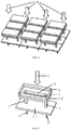
FIG. 5 shows a schematic structural diagram of a terahertz detector according to another exemplary embodiment of the present disclosure, where the terahertz detector includes a plurality of detection units arranged in a plane array. -
FIG. 6 shows a schematic structural diagram of a detection unit of the terahertz detector shown inFIG. 5 . - Although the present disclosure will be fully described with reference to the drawings containing the preferred embodiments of the present disclosure, it should be understood that those skilled in the art may modify the present disclosure while obtaining the technical effects of the present disclosure. Therefore, it should be understood that the above description is a broad disclosure for those ordinary skilled in the art, and its content is not intended to limit the exemplary embodiments described in the present disclosure.
- In addition, in the following detailed description, for the convenience of explanation, many specific details are set forth to provide a comprehensive understanding of the embodiments of the present disclosure. Obviously, however, one or more embodiments may also be implemented without these specific details. In other cases, well-known structures and devices are shown in diagrammatic form to simplify the drawings.
- According to a general inventive concept of the present disclosure, there is provided a terahertz detector, including a substrate and at least one detection unit. Each detection unit includes: a channel material arranged on the substrate, two electrodes respectively in ohmic contact with both ends of the channel material in a longitudinal direction, and three-dimensional graphene in direct or indirect thermal contact with the channel material.
-
FIG. 1 shows a schematic structural diagram of a terahertz detector according to an exemplary embodiment of the present disclosure. As shown inFIG. 1 , the terahertz detector includes asubstrate 2 and a detection unit. Thesubstrate 2 is suitable for providing a stable mechanical support for the entire terahertz detector. It is a single-layer cuboid sheet formed of suitable thermoelectric materials including but are not limited to high-resistance silicon, silicon nitride, silicon dioxide, silicate glass, and so on. The detection unit includes achannel material 1, twoelectrodes dimensional graphene 5. Thechannel material 1 is located on thesubstrate 2 and is used to convert heat conducted from the three-dimensional graphene 5 into an electrical signal that is convenient for direct detection. Thechannel material 1 may be formed of materials with good thermoelectric properties, including but not limited to graphene, carbon nanotubes, transition metal chalcogenides, and so on. Theelectrodes channel material 1 in the longitudinal direction, and form a good ohmic contact with thechannel material 1, so as to transmit the electrical signal generated by thechannel material 1 to an electrical detection instrument (not shown)) for measurement. Theelectrodes dimensional graphene 5 is connected to thesubstrate 2 and is located above a contact between theelectrode 3 and thechannel material 1, and is in direct thermal contact with theelectrode 3 and thechannel material 1. - When in use, the terahertz detector is firstly fixed on a firm and reliable optical support to face a
terahertz wave 6 to be measured. When theterahertz wave 6 to be measured irradiates a surface of the detector, the three-dimensional graphene 5 may absorb theterahertz wave 6 to be measured and transfer energy to thechannel material 1 in the form of heat, which may cause an increase of a temperature at an end of thechannel material 1 close to theelectrode 3. As a result, a temperature difference is formed at both ends of thechannel material 1, which leads to a photothermoelectric effect and generates a thermoelectromotive force between theelectrodes terahertz wave 6 to be measured may be obtained. - The three-
dimensional graphene 5 is formed of thin layers of graphene densely staggered in a three-dimensional space and has a certain mechanical strength. In the three-dimensional graphene 5, many pore structures of varying sizes are formed between the thin layers of graphene. The size of these pores is on the order of tens of microns to hundreds of microns, which corresponds to a wavelength of the terahertz wave. Therefore, the terahertz wave incident on the surface of the three-dimensional graphene 5 may be strongly scattered and diffracted, and repeatedly oscillate in the three-dimensional graphene 5, and thus largely absorbed by the three-dimensional graphene. According to statistics, absorptivity of the three-dimensional graphene 5 in the terahertz band may generally reach more than 99%. By using the three-dimensional graphene 5 as an absorber, the detector proposed in the present disclosure may solve the problem of insufficient absorption of theterahertz wave 6 to be measured by thechannel material 1, so that the response sensitivity of the detector may be effectively improved. - In addition, the three-
dimensional graphene 5 may achieve efficient absorption of terahertz waves of full band, large incident angle and arbitrary polarization state, as long as theterahertz wave 6 irradiates a front of the device. Therefore, the terahertz detector has advantages of wide operation bandwidth, strong angle adaptability, and no difference in polarization, so that the terahertz detector may have a broader application range and better stability than a detector that relies on an antenna to collect theterahertz wave 6. - In the terahertz detector provided by this embodiment, the three-
dimensional graphene 5 is in direct or indirect thermal contact with one end of thechannel material 1 in the longitudinal direction so as to obtain an asymmetrical absorption effect. In this way, the detector may operate in a uniform terahertz field environment, which makes the detector easy to integrate and more practical. Moreover, a shape, a size and a position of the three-dimensional graphene 5 may be flexibly adjusted, which provides convenience for overcoming shortcomings of detection mechanism and improving performance of the detection device. - It should be noted that although the terahertz detector in the embodiments described above performs detection through the photothermalelectric effect, those skilled in the art should understand that in some other embodiments of the present disclosure, radiant thermal effect and pyroelectric effect may also be used.
-
FIG. 2 shows a terahertz detector according to another exemplary embodiment of the present disclosure. As shown inFIG. 2 , the terahertz detector includes asubstrate 2 and a detection unit. Different from the embodiment shown inFIG. 1 , thesubstrate 2 has a U-shaped structure, and both ends of thechannel material 1 are respectively fixed on twoside portions 22 of the U-shaped structure, so that a middle portion of thechannel material 1 is suspended, that is, not in contact with thesubstrate 2. The three-dimensional graphene 5 is arranged between a bottom 21 of the U-shaped structure and thechannel material 1. - As shown in
FIG. 2 , in an exemplary embodiment, a bottom of the three-dimensional graphene 5 is firmly connected to the bottom 21 of the substrate, and a top of the three-dimensional graphene 5 is in thermal contact with thechannel material 1. For example, the three-dimensional graphene 5 may be adhered to thechannel material 1 through conductive silica gel. - As shown in
FIG. 1 and FIG. 2 , in some embodiments, both ends of theelectrodes channel material 1 in a direction perpendicular to the longitudinal direction of thechannel material 1, and are connected (for example, adhered) to thesubstrate 2. - As shown in
FIG. 1 and FIG. 2 , in some embodiments, the three-dimensional graphene 5 has a cuboid shape with a long side parallel to the longitudinal direction of thechannel material 1, so as to increase a contact area with thechannel material 1. It should be noted that in some other embodiments of the present disclosure, the three-dimensional graphene 5 may also be implemented to have other shapes, such as a shape with an isosceles trapezoid cross section. -
FIG. 3 and FIG. 4 show a terahertz detector according to another exemplary embodiment of the present disclosure. As shown inFIG. 3 and FIG. 4 , the terahertz detector includes asubstrate 2 and a plurality of detection units arranged in a linear array. Thesubstrate 2 includes a first substrate 2-1 and a second substrate 2-2 substantially parallel to and arranged at a certain distance from the first substrate 2-1. Thechannel material 1 of each detection unit has a first end in the longitudinal direction that is connected to the first substrate 2-1, and a second end in the longitudinal direction that is connected to the second substrate 2-2 and protrudes from a side of the second substrate 2-2 away from the first substrate 2-1. Theelectrode 4 is arranged on the first substrate 2-1 and forms a good ohmic contact with the first end of thechannel material 1. Theelectrode 3 is arranged on the second substrate 2-2 and forms a good ohmic contact with the second end of thechannel material 1. The three-dimensional graphene 5 is arranged on the second substrate 2-2 and forms good thermal contact with the second end of thechannel material 1. The three-dimensional graphene 5 may completely cover the second end of thechannel material 1 and a part of theelectrode 3. - Although a plurality of detection units arranged in a linear array are shown in this embodiment, it should be noted that in some other embodiments of the present disclosure, it is also possible to provide only one such detection unit or a plurality of such detection units arranged in a plane array.
-
FIG. 5 and FIG. 6 show a terahertz detector according to yet another exemplary embodiment of the present disclosure. As shown inFIG. 5 and FIG. 6 , the terahertz detector includes asubstrate 2 and a plurality of detection units arranged in a plane array. Thesubstrate 2 includes a first substrate 2-1 and a plurality of second substrates 2-2' substantially parallel to and arranged at a certain distance from the first substrate 2-1. The plurality of detection units are arranged in one-to-one correspondence with the plurality of second substrates 2-2', and thechannel material 1 of each detection unit is arranged on the second substrate 2-2'. First ends of theelectrodes electrodes channel material 1 arranged on the second substrate 2-2' in the longitudinal direction. The three-dimensional graphene 5 is arranged on the second substrate 2-2' and is in indirect thermal contact with thechannel material 1. The terahertz detector may perform the detection through pyroelectric effect. When theterahertz wave 6 to be measured irradiates the surface of the detector, the three-dimensional graphene 5 may absorb theterahertz wave 6 and transfer energy to thechannel material 1 in the form of heat to causes an increase of the temperature of thechannel material 1, which leads to a pyroelectric effect and generates thermoelectromotive force between theelectrodes terahertz wave 6 to be measured may be obtained - As shown in
FIG. 6 , each second substrate 2-2' is further provided with an insulating and thermallyconductive layer 7 covering thechannel material 1, and the three-dimensional graphene 5 is arranged on a side of the insulating and thermallyconductive layer 7 away from thechannel material 1. In this way, the insulating and thermallyconductive layer 7 has a good thermal contact with the three-dimensional graphene 5 and thechannel material 1, so that an indirect thermal contact is formed between the three-dimensional graphene 5 and thechannel material 1. It should be noted that in some other embodiments of the present disclosure, the insulating and thermallyconductive layer 7 may not be provided, so that thechannel material 1 is in direct thermal contact with the three-dimensional graphene 5. - Although a plurality of detection units arranged in a plane array are shown in this embodiment, it should be noted that in some other embodiments of the present disclosure, it is also possible to provide only one such detection unit or a plurality of such detection units arranged in a linear array.
- As shown in
FIG. 6 , in an exemplary embodiment, the first ends of theelectrodes pin structures 31 and 34, to facilitate connection with a circuit. - In an exemplary embodiment not shown in the present disclosure, the terahertz detector further includes a wire or a chip suitable for connecting the
electrodes terahertz wave 6 to be measured may be obtained by reading an electrical quantity change on the electrical detection device. According to specific detection principles, the electrical quantities that may be measured include but are not limited to voltage, current, resistance, capacitance, and so on. The electrical detection device here includes, but is not limited to, digital source meter, oscilloscope, and lock-in amplifier. It should be noted that in a case that the terahertz detector includes a plurality of detector units arranged in a linear array or a plane array, the terahertz detector may further include a corresponding electrical signal processing module used to process electrical signals of the plurality of detection units. - The present disclosure further provides a method of manufacturing the terahertz detector described above, including following steps.
- In
step 1, thechannel material 1 is prepared. Thechannel material 1 may be used to grow a single layer of graphene, for example, by a chemical vapor deposition method. The single layer of graphene may be then transferred to filter paper, and the filter paper may be cut into narrow strips of appropriate size as thechannel material 1. - In
step 2, thecut channel material 1 is transferred to thesubstrate 2. - In
step 3, a mask is drawn, and twoelectrodes channel material 1 by using a mask evaporation method. - In
step 4, the three-dimensional graphene 5 is prepared. For example, a three-dimensional graphene block may be prepared by a hydration heat method, and cut into a shape with an appropriate size by using a laser cutting method. - In
step 5, the three-dimensional graphene 5 may be fixed to thechannel material 1, for example, by using thermally conductive silica gel with good thermal conductivity. - After the preparation is completed, a resistivity between the
electrodes - Those skilled in the art may understand that the embodiments described above are exemplary, and those skilled in the art may make improvements. The structures described in the embodiments may be combined freely without conflicts in structure or principle.
- After describing the preferred embodiments of the present disclosure in detail, those skilled in the art may clearly understand that various changes and modifications may be made without departing from the scope and spirit of the appended claims, and the present disclosure is not limited to implementations of the exemplary embodiments described in the present disclosure.
Claims (13)
- A terahertz detector, comprising:a substrate; andat least one detection unit, wherein each detection unit comprises:a channel material arranged on the substrate,two electrodes respectively in ohmic contact with both ends of the channel material in a longitudinal direction, anda three-dimensional graphene in direct or indirect thermal contact with the channel material.
- The terahertz detector of claim 1, wherein the three-dimensional graphene is in direct or indirect thermal contact with one end of the channel material.
- The terahertz detector of claim 2, wherein the three-dimensional graphene is arranged at a contact between the channel material and the electrode.
- The terahertz detector of claim 1, wherein the substrate has a U-shaped structure, both ends of the channel material in the longitudinal direction are respectively fixed on both side portions of the U-shaped structure, and the three-dimensional graphene is arranged between a bottom of the U-shaped structure and the channel material.
- The terahertz detector of claim 1, wherein the three-dimensional graphene is adhered to the channel material.
- The terahertz detector of claim 1, wherein each electrode has two ends that extend to an outside of the channel material in a direction perpendicular to the longitudinal direction of the channel material and that are connected to the substrate.
- The terahertz detector of any one of claims 1 to 6, wherein the three-dimensional graphene has a cuboid structure with a long side parallel to the longitudinal direction of the channel
- The terahertz detector of claim 1, wherein the substrate comprises a first substrate and a second substrate arranged at a distance from the first substrate, the channel material of each detection unit has a first end in the longitudinal direction that is connected to the first substrate, and a second end in the longitudinal direction protruding from a side of the second substrate away from the first substrate, both electrodes of each detection unit are respectively arranged on the first substrate and the second substrate, and the three-dimensional graphene is arranged on the second substrate and is in thermal contact with the second end of the channel material protruding from the second substrate.
- The terahertz detector of claim 1, wherein the substrate comprises a first substrate and at least one second substrate arranged at a distance from the first substrate, the at least one detection unit is arranged in a one-to-one correspondence with the at least one second substrate; wherein the channel material of each detection unit is arranged on the second substrate, first ends of both electrodes of each detection unit are connected to the first substrate and protrude from a side of the first substrate away from the second substrate, and second ends of both electrodes of the each detection unit are in ohmic contact with both ends of the channel material arranged on the second substrate in the longitudinal direction, and the three-dimensional graphene is arranged on the second substrate.
- The terahertz detector of claim 9, further comprising an insulating and thermally conductive layer arranged between the channel material and the three-dimensional graphene.
- The terahertz detector of claim 9, wherein the first end of each electrode is provided with a tapered pin structure.
- The terahertz detector of any one of claims 8 to 11, wherein the plurality of detection units are arranged in a plane array or a linear array.
- A method of manufacturing a terahertz detector, comprising:preparing a channel material;transferring the channel material to a substrate;making two electrodes on both ends of the channel material;preparing a three-dimensional graphene; andfixing the three-dimensional graphene to the channel material.
Applications Claiming Priority (2)
| Application Number | Priority Date | Filing Date | Title |
|---|---|---|---|
| CN201811631501.4A CN109494293B (en) | 2018-12-28 | 2018-12-28 | Terahertz detector and method for manufacturing the same |
| PCT/CN2019/110339 WO2020134327A1 (en) | 2018-12-28 | 2019-10-10 | Terahertz detector and manufacturing method therefor |
Publications (3)
| Publication Number | Publication Date |
|---|---|
| EP3905351A1 true EP3905351A1 (en) | 2021-11-03 |
| EP3905351A4 EP3905351A4 (en) | 2022-12-21 |
| EP3905351B1 EP3905351B1 (en) | 2025-11-19 |
Family
ID=65713208
Family Applications (1)
| Application Number | Title | Priority Date | Filing Date |
|---|---|---|---|
| EP19901843.3A Active EP3905351B1 (en) | 2018-12-28 | 2019-10-10 | Terahertz detector and manufacturing method therefor |
Country Status (4)
| Country | Link |
|---|---|
| US (1) | US12004426B2 (en) |
| EP (1) | EP3905351B1 (en) |
| CN (1) | CN109494293B (en) |
| WO (1) | WO2020134327A1 (en) |
Families Citing this family (6)
| Publication number | Priority date | Publication date | Assignee | Title |
|---|---|---|---|---|
| CN109494293B (en) | 2018-12-28 | 2024-09-13 | 同方威视技术股份有限公司 | Terahertz detector and method for manufacturing the same |
| CN110044476B (en) * | 2019-04-04 | 2021-02-12 | 中国科学院上海技术物理研究所 | Terahertz detector based on antiferromagnetic nonmagnetic metal heterojunction |
| CN110148643B (en) * | 2019-06-06 | 2021-05-04 | 上海纳米技术及应用国家工程研究中心有限公司 | Construction of semiconductor quantum dot/graphene van der Waals junction flexible devices |
| CN110687358B (en) * | 2019-10-14 | 2022-05-13 | 云南师范大学 | Capacitive electromagnetic wave detector and system based on pyroelectric material |
| CN110767769B (en) * | 2019-10-29 | 2025-12-16 | 清华大学 | Detection unit, ultra-wideband light detector and detection method |
| CN113175991A (en) * | 2021-03-19 | 2021-07-27 | 清华大学 | Detection device and method for realizing terahertz wave detection |
Family Cites Families (17)
| Publication number | Priority date | Publication date | Assignee | Title |
|---|---|---|---|---|
| JP5691524B2 (en) * | 2011-01-05 | 2015-04-01 | ソニー株式会社 | Graphene film transfer method and transparent conductive film manufacturing method |
| CN103575407A (en) | 2012-07-18 | 2014-02-12 | 北京大学 | Terahertz radiation detector |
| GB2516443A (en) * | 2013-07-22 | 2015-01-28 | Nokia Corp | An apparatus for sensing |
| US9797779B2 (en) * | 2013-12-05 | 2017-10-24 | National University Of Singapore | Pyroelectric detector using graphene electrode |
| CN104465850B (en) * | 2014-11-28 | 2016-09-21 | 电子科技大学 | Pyroelectric infrared detector based on Graphene absorbed layer and manufacture method thereof |
| CN104993056A (en) * | 2015-06-11 | 2015-10-21 | 上海电力学院 | Wide-spectrum flexible photoelectric detector and making method thereof |
| WO2016209666A2 (en) * | 2015-06-15 | 2016-12-29 | University Of Maryland, College Park | Hybrid metal-graphene terahertz optoelectronic system with tunable plasmonic resonance and method of fabrication |
| EP3220113B1 (en) * | 2016-03-16 | 2019-05-01 | Centre National de la Recherche Scientifique - CNRS - | Optomechanical transducer for terahertz electromagnetic waves |
| US10969335B2 (en) * | 2016-04-28 | 2021-04-06 | Tokyo Institute Of Technology | Terahertz wave detection device and array sensor |
| CN105957955B (en) * | 2016-07-19 | 2018-10-23 | 中国科学院重庆绿色智能技术研究院 | A kind of photodetector based on graphene planes knot |
| US10121926B2 (en) * | 2016-08-22 | 2018-11-06 | Shahid Rajaee Teacher Training University | Graphene-based detector for W-band and terahertz radiations |
| EP3296028A1 (en) * | 2016-09-15 | 2018-03-21 | Paul Scherrer Institut | Transducer for electromagnetic and thermo-acoustic wave based on three dimensional graphene structure |
| JP7149536B2 (en) * | 2017-05-09 | 2022-10-07 | 国立大学法人東京工業大学 | Carbon nanotube film, terahertz wave detector, and method for forming PN junction of carbon nanotube film |
| CN107482109A (en) * | 2017-07-02 | 2017-12-15 | 中国科学院上海微系统与信息技术研究所 | A room temperature terahertz detector based on graphene pyroelectric effect and its preparation method |
| CN107720728A (en) * | 2017-09-15 | 2018-02-23 | 南开大学 | A kind of terahertz electromagnetic wave stealth material based on graphene |
| CN209232819U (en) * | 2018-12-28 | 2019-08-09 | 同方威视技术股份有限公司 | Terahertz detector |
| CN109494293B (en) * | 2018-12-28 | 2024-09-13 | 同方威视技术股份有限公司 | Terahertz detector and method for manufacturing the same |
-
2018
- 2018-12-28 CN CN201811631501.4A patent/CN109494293B/en active Active
-
2019
- 2019-10-10 EP EP19901843.3A patent/EP3905351B1/en active Active
- 2019-10-10 US US17/418,967 patent/US12004426B2/en active Active
- 2019-10-10 WO PCT/CN2019/110339 patent/WO2020134327A1/en not_active Ceased
Also Published As
| Publication number | Publication date |
|---|---|
| EP3905351B1 (en) | 2025-11-19 |
| US20220115576A1 (en) | 2022-04-14 |
| EP3905351A4 (en) | 2022-12-21 |
| CN109494293B (en) | 2024-09-13 |
| US12004426B2 (en) | 2024-06-04 |
| CN109494293A (en) | 2019-03-19 |
| WO2020134327A1 (en) | 2020-07-02 |
Similar Documents
| Publication | Publication Date | Title |
|---|---|---|
| US12004426B2 (en) | Terahertz detector and method of manufacturing terahertz detector | |
| JP5684487B2 (en) | Bolometer detector for detecting electromagnetic radiation in the infrared to terahertz frequency band, and array detection apparatus having such a detector | |
| CN105514128B (en) | A kind of graphene room temperature terahertz wave detector and preparation method | |
| KR102040149B1 (en) | Infrared detector | |
| US7851761B2 (en) | Multi-band terahertz receiver and imaging device | |
| WO2016140946A1 (en) | Plasmon-enhanced terahertz graphene-based photodetector and method of fabrication | |
| US20250283762A1 (en) | Photodetector pixel, photodetector and methods of forming the same | |
| CN111060466B (en) | Portable optical gas sensor | |
| CN215418202U (en) | Terahertz detector that room temperature binary channels can be regulated and control | |
| Li et al. | Design strategies toward plasmon-enhanced 2-dimensional material photodetectors | |
| CN113049096A (en) | Nickel telluride terahertz detector integrated with room-temperature periodic logarithmic antenna and preparation method | |
| CN114784128A (en) | Topology-enhanced antimony telluride terahertz photoelectric detector based on butterfly antenna structure and preparation method thereof | |
| US9052231B2 (en) | Bolometric detector of an electromagnetic radiation in the terahertz range | |
| CN110767769B (en) | Detection unit, ultra-wideband light detector and detection method | |
| Chen et al. | Monolithic multiparameter terahertz nano/microdetector based on plasmon polariton atomic cavity | |
| CN110246914A (en) | A kind of enhanced terahertz detector of etching based on indium antimonide and preparation method | |
| CN209232819U (en) | Terahertz detector | |
| CN110864805B (en) | Ultra-wideband spectrum detection device and method | |
| CN113363344A (en) | Room-temperature dual-channel adjustable terahertz detector and preparation method thereof | |
| CN114689179A (en) | Surface plasmon metamaterial pyroelectric hyperspectral imaging system | |
| Xiong et al. | Design of a Broadband Microwave Power Detector Based on Metasurfaces With Linear Response and Thermal Sensing | |
| CN210956702U (en) | Detection unit and ultra-wideband photodetector | |
| Zhang et al. | Active and accurate temperature control of terahertz functional devices using a micro-hotplate system | |
| CN105182462B (en) | A kind of middle infrared polarization converter based on double-rod antenna structure | |
| CN108508267A (en) | Micro-nano electronic mechanical system direct-heating type microwave radiometer based on clamped beam |
Legal Events
| Date | Code | Title | Description |
|---|---|---|---|
| STAA | Information on the status of an ep patent application or granted ep patent |
Free format text: STATUS: THE INTERNATIONAL PUBLICATION HAS BEEN MADE |
|
| PUAI | Public reference made under article 153(3) epc to a published international application that has entered the european phase |
Free format text: ORIGINAL CODE: 0009012 |
|
| STAA | Information on the status of an ep patent application or granted ep patent |
Free format text: STATUS: REQUEST FOR EXAMINATION WAS MADE |
|
| 17P | Request for examination filed |
Effective date: 20210727 |
|
| AK | Designated contracting states |
Kind code of ref document: A1 Designated state(s): AL AT BE BG CH CY CZ DE DK EE ES FI FR GB GR HR HU IE IS IT LI LT LU LV MC MK MT NL NO PL PT RO RS SE SI SK SM TR |
|
| DAV | Request for validation of the european patent (deleted) | ||
| DAX | Request for extension of the european patent (deleted) | ||
| A4 | Supplementary search report drawn up and despatched |
Effective date: 20221118 |
|
| RIC1 | Information provided on ipc code assigned before grant |
Ipc: G01J 5/12 20060101ALI20221114BHEP Ipc: H01L 37/02 20060101AFI20221114BHEP |
|
| REG | Reference to a national code |
Ref country code: DE Ref legal event code: R079 Free format text: PREVIOUS MAIN CLASS: H01L0037020000 Ipc: H10N0015200000 Ref document number: 602019078379 Country of ref document: DE |
|
| RIC1 | Information provided on ipc code assigned before grant |
Ipc: G01J 5/12 20060101ALI20250522BHEP Ipc: H10N 15/20 20230101AFI20250522BHEP |
|
| REG | Reference to a national code |
Ref country code: DE Ref legal event code: R079 Free format text: PREVIOUS MAIN CLASS: H10N0015200000 Ipc: H10N0015000000 Ref document number: 602019078379 Country of ref document: DE |
|
| RIC1 | Information provided on ipc code assigned before grant |
Ipc: H10N 15/20 20230101AFI20250606BHEP Ipc: G01J 5/34 20060101ALI20250606BHEP |
|
| GRAP | Despatch of communication of intention to grant a patent |
Free format text: ORIGINAL CODE: EPIDOSNIGR1 |
|
| STAA | Information on the status of an ep patent application or granted ep patent |
Free format text: STATUS: GRANT OF PATENT IS INTENDED |
|
| RIC1 | Information provided on ipc code assigned before grant |
Ipc: H10N 15/00 20230101AFI20250630BHEP Ipc: G01J 5/34 20060101ALI20250630BHEP |
|
| INTG | Intention to grant announced |
Effective date: 20250729 |
|
| GRAS | Grant fee paid |
Free format text: ORIGINAL CODE: EPIDOSNIGR3 |
|
| GRAA | (expected) grant |
Free format text: ORIGINAL CODE: 0009210 |
|
| STAA | Information on the status of an ep patent application or granted ep patent |
Free format text: STATUS: THE PATENT HAS BEEN GRANTED |
|
| AK | Designated contracting states |
Kind code of ref document: B1 Designated state(s): AL AT BE BG CH CY CZ DE DK EE ES FI FR GB GR HR HU IE IS IT LI LT LU LV MC MK MT NL NO PL PT RO RS SE SI SK SM TR |
|
| REG | Reference to a national code |
Ref country code: CH Ref legal event code: F10 Free format text: ST27 STATUS EVENT CODE: U-0-0-F10-F00 (AS PROVIDED BY THE NATIONAL OFFICE) Effective date: 20251119 Ref country code: GB Ref legal event code: FG4D |
|
| REG | Reference to a national code |
Ref country code: DE Ref legal event code: R096 Ref document number: 602019078379 Country of ref document: DE |
|
| REG | Reference to a national code |
Ref country code: IE Ref legal event code: FG4D |
|
| REG | Reference to a national code |
Ref country code: NL Ref legal event code: MP Effective date: 20251119 |
|
| PG25 | Lapsed in a contracting state [announced via postgrant information from national office to epo] |
Ref country code: ES Free format text: LAPSE BECAUSE OF FAILURE TO SUBMIT A TRANSLATION OF THE DESCRIPTION OR TO PAY THE FEE WITHIN THE PRESCRIBED TIME-LIMIT Effective date: 20251119 |
|
| REG | Reference to a national code |
Ref country code: LT Ref legal event code: MG9D |
|
| PG25 | Lapsed in a contracting state [announced via postgrant information from national office to epo] |
Ref country code: NO Free format text: LAPSE BECAUSE OF FAILURE TO SUBMIT A TRANSLATION OF THE DESCRIPTION OR TO PAY THE FEE WITHIN THE PRESCRIBED TIME-LIMIT Effective date: 20260219 |
|
| PG25 | Lapsed in a contracting state [announced via postgrant information from national office to epo] |
Ref country code: HR Free format text: LAPSE BECAUSE OF FAILURE TO SUBMIT A TRANSLATION OF THE DESCRIPTION OR TO PAY THE FEE WITHIN THE PRESCRIBED TIME-LIMIT Effective date: 20251119 Ref country code: FI Free format text: LAPSE BECAUSE OF FAILURE TO SUBMIT A TRANSLATION OF THE DESCRIPTION OR TO PAY THE FEE WITHIN THE PRESCRIBED TIME-LIMIT Effective date: 20251119 Ref country code: AT Free format text: LAPSE BECAUSE OF FAILURE TO SUBMIT A TRANSLATION OF THE DESCRIPTION OR TO PAY THE FEE WITHIN THE PRESCRIBED TIME-LIMIT Effective date: 20251119 |
|
| REG | Reference to a national code |
Ref country code: AT Ref legal event code: MK05 Ref document number: 1860074 Country of ref document: AT Kind code of ref document: T Effective date: 20251119 |
|
| PG25 | Lapsed in a contracting state [announced via postgrant information from national office to epo] |
Ref country code: NL Free format text: LAPSE BECAUSE OF FAILURE TO SUBMIT A TRANSLATION OF THE DESCRIPTION OR TO PAY THE FEE WITHIN THE PRESCRIBED TIME-LIMIT Effective date: 20251119 |
|
| PG25 | Lapsed in a contracting state [announced via postgrant information from national office to epo] |
Ref country code: RS Free format text: LAPSE BECAUSE OF FAILURE TO SUBMIT A TRANSLATION OF THE DESCRIPTION OR TO PAY THE FEE WITHIN THE PRESCRIBED TIME-LIMIT Effective date: 20260219 |
|
| PG25 | Lapsed in a contracting state [announced via postgrant information from national office to epo] |
Ref country code: IS Free format text: LAPSE BECAUSE OF FAILURE TO SUBMIT A TRANSLATION OF THE DESCRIPTION OR TO PAY THE FEE WITHIN THE PRESCRIBED TIME-LIMIT Effective date: 20260319 |
|
| PG25 | Lapsed in a contracting state [announced via postgrant information from national office to epo] |
Ref country code: PT Free format text: LAPSE BECAUSE OF FAILURE TO SUBMIT A TRANSLATION OF THE DESCRIPTION OR TO PAY THE FEE WITHIN THE PRESCRIBED TIME-LIMIT Effective date: 20260319 |
|
| PG25 | Lapsed in a contracting state [announced via postgrant information from national office to epo] |
Ref country code: PL Free format text: LAPSE BECAUSE OF FAILURE TO SUBMIT A TRANSLATION OF THE DESCRIPTION OR TO PAY THE FEE WITHIN THE PRESCRIBED TIME-LIMIT Effective date: 20251119 |
|
| PG25 | Lapsed in a contracting state [announced via postgrant information from national office to epo] |
Ref country code: LV Free format text: LAPSE BECAUSE OF FAILURE TO SUBMIT A TRANSLATION OF THE DESCRIPTION OR TO PAY THE FEE WITHIN THE PRESCRIBED TIME-LIMIT Effective date: 20251119 |
|
| PG25 | Lapsed in a contracting state [announced via postgrant information from national office to epo] |
Ref country code: BG Free format text: LAPSE BECAUSE OF FAILURE TO SUBMIT A TRANSLATION OF THE DESCRIPTION OR TO PAY THE FEE WITHIN THE PRESCRIBED TIME-LIMIT Effective date: 20251119 |