EP3899690B1 - Aufrechterhaltung der richtigen spannungssequenz bei plötzlichem stromausfall - Google Patents
Aufrechterhaltung der richtigen spannungssequenz bei plötzlichem stromausfall Download PDFInfo
- Publication number
- EP3899690B1 EP3899690B1 EP19898065.8A EP19898065A EP3899690B1 EP 3899690 B1 EP3899690 B1 EP 3899690B1 EP 19898065 A EP19898065 A EP 19898065A EP 3899690 B1 EP3899690 B1 EP 3899690B1
- Authority
- EP
- European Patent Office
- Prior art keywords
- voltage
- output
- capacitor
- circuit
- time
- Prior art date
- Legal status (The legal status is an assumption and is not a legal conclusion. Google has not performed a legal analysis and makes no representation as to the accuracy of the status listed.)
- Active
Links
Images


Classifications
-
- G—PHYSICS
- G01—MEASURING; TESTING
- G01R—MEASURING ELECTRIC VARIABLES; MEASURING MAGNETIC VARIABLES
- G01R19/00—Arrangements for measuring currents or voltages or for indicating presence or sign thereof
- G01R19/165—Indicating that current or voltage is either above or below a predetermined value or within or outside a predetermined range of values
- G01R19/16533—Indicating that current or voltage is either above or below a predetermined value or within or outside a predetermined range of values characterised by the application
- G01R19/16538—Indicating that current or voltage is either above or below a predetermined value or within or outside a predetermined range of values characterised by the application in AC or DC supplies
- G01R19/16552—Indicating that current or voltage is either above or below a predetermined value or within or outside a predetermined range of values characterised by the application in AC or DC supplies in I.C. power supplies
-
- G—PHYSICS
- G05—CONTROLLING; REGULATING
- G05F—SYSTEMS FOR REGULATING ELECTRIC OR MAGNETIC VARIABLES
- G05F1/00—Automatic systems in which deviations of an electric quantity from one or more predetermined values are detected at the output of the system and fed back to a device within the system to restore the detected quantity to its predetermined value or values, i.e. retroactive systems
- G05F1/10—Regulating voltage or current
- G05F1/46—Regulating voltage or current wherein the variable actually regulated by the final control device is DC
- G05F1/56—Regulating voltage or current wherein the variable actually regulated by the final control device is DC using semiconductor devices in series with the load as final control devices
- G05F1/565—Regulating voltage or current wherein the variable actually regulated by the final control device is DC using semiconductor devices in series with the load as final control devices sensing a condition of the system or its load in addition to means responsive to deviations in the output of the system, e.g. current, voltage, power factor
- G05F1/569—Regulating voltage or current wherein the variable actually regulated by the final control device is DC using semiconductor devices in series with the load as final control devices sensing a condition of the system or its load in addition to means responsive to deviations in the output of the system, e.g. current, voltage, power factor for protection
-
- G—PHYSICS
- G06—COMPUTING OR CALCULATING; COUNTING
- G06F—ELECTRIC DIGITAL DATA PROCESSING
- G06F1/00—Details not covered by groups G06F3/00 - G06F13/00 and G06F21/00
- G06F1/26—Power supply means, e.g. regulation thereof
-
- G—PHYSICS
- G06—COMPUTING OR CALCULATING; COUNTING
- G06F—ELECTRIC DIGITAL DATA PROCESSING
- G06F1/00—Details not covered by groups G06F3/00 - G06F13/00 and G06F21/00
- G06F1/26—Power supply means, e.g. regulation thereof
- G06F1/28—Supervision thereof, e.g. detecting power-supply failure by out of limits supervision
-
- G—PHYSICS
- G06—COMPUTING OR CALCULATING; COUNTING
- G06F—ELECTRIC DIGITAL DATA PROCESSING
- G06F1/00—Details not covered by groups G06F3/00 - G06F13/00 and G06F21/00
- G06F1/26—Power supply means, e.g. regulation thereof
- G06F1/30—Means for acting in the event of power-supply failure or interruption, e.g. power-supply fluctuations
-
- H—ELECTRICITY
- H02—GENERATION; CONVERSION OR DISTRIBUTION OF ELECTRIC POWER
- H02J—ELECTRIC POWER NETWORKS; CIRCUIT ARRANGEMENTS OR SYSTEMS FOR SUPPLYING OR DISTRIBUTING ELECTRIC POWER; SYSTEMS FOR STORING ELECTRIC ENERGY
- H02J1/00—Circuit arrangements for DC mains or DC distribution networks
- H02J1/14—Balancing load and power generation in DC networks
Definitions
- Various embodiments of the invention relate to controlling power to digital integrated circuits with an intention of avoiding damage to the integrated circuits as a result of a sudden loss of the source power.
- EP2003532A2 relates to a power supply apparatus that supplies an operating voltage to a microcomputer.
- the power supply apparatus is to reliably reset the microcomputer before operation becomes unstable when an external power supply voltage decreases due to interruption.
- An externally supplied power supply voltage is stepped down to generate an intermediate voltage.
- the intermediate voltage is stepped down to generate an operating voltage for a micro-computer core.
- the intermediate voltage is stepped down to generate an operating voltage for an I/O port.
- the power supply apparatus outputs a reset signal to the microcomputer.
- the microcomputer can reliably reset and the core can be prevented from operating erratically before the voltage becomes lower than a minimum core operating voltage.
- EP3410591A1 relates to an energy supply system for a multi-voltage electronic device.
- references to “one embodiment”, “an embodiment”, “example embodiment”, “various embodiments”, etc., indicate that the embodiment(s) of the invention so described may include particular features, structures, or characteristics, but not every embodiment necessarily includes the particular features, structures, or characteristics. Further, some embodiments may have some or all of the features described for other embodiments.
- Fig. 1A shows a circuit to produce multiple voltage rails, without various improvements of the invention.
- a source voltage VIN powers two voltage regulators 110 and 150, which provide power to a device 160.
- the term 'source voltage' refers to the common input voltage for the multiple voltage regulators.
- An example of the indicated source voltage is shown as +12V DC, but other values may be used.
- Only two voltage regulators are shown, with VR 1 being represented as outputing the higher voltage V H , and VR 2 outputing the lower voltage V L . Other numbers of voltage regulators may be used, but these two serve illustrate one example.
- inductors L 1 and L 2 are shown at the output of voltage regulators VR 1 and VR 2 , respectively, and may be used to smooth out ripples in those two outputs. Other embodiments may not have these inductors.
- Capacitors C 1 and C 2 are shown at the output of the inductors (or alternately at the outputs of the voltage regulators), and may be used to further smooth out voltages V H and VL , and to provide charge storage capacity on those outputs. These voltage may then provided to the loads.
- the loads are in a device 160, which is shown as a central processing unit (CPU) or dual in-line memory module (DIMM), but other devices may be used.
- CPU central processing unit
- DIMM dual in-line memory module
- Fig.1B shows a diagram of voltage rails after a loss of source power to the circuit of Fig. 1A .
- the diagram shows V H and V L at constant levels until time t 1 , at which point source voltage VIN may be lost. This in turn may cause V H and V L to begin dropping as shown.
- V H may drop faster than V L until is drops lower than V L at time t 2 and beyond. This reverse-voltage condition may cause damage to sensitive circuit components in the load.
- Fig. 2A shows a circuit to produce multiple voltage rails, with protective circuitry according to an embodiment of the invention.
- the general components VR 1 and VR 2 , L 1 and L 2 , C 1 , and C 2 , and CPU or DIMM may be as shown in Fig. 1A .
- Power Loss Trigger Generator Circuit 210 may be used to detect a loss of source voltage VIN, and use that detection to generate an Event Trigger Signal.
- the event trigger signal in this case may be a signal to the Sequence Control Circuit 250 indicating that source voltage VIN has been lost, and this signal may be then be used to activate the Sequence Control Circuit 250.
- VIN may cause a loss of input power VIN 1 to VR 1 and VIN 2 to VR 2
- two components may be added to cause VIN 1 and VIN 2 to react differently.
- Capacitor C hold-up may cause VIN 1 to drop more slowly than VIN 2 . Without more, this might keep V H from dropping as quickly as it did in Fig. 1A .
- the amount of time it takes V H to drop below V L may be longer than in Fig. 1B . However, V H may still evenually drop below V L , so the problem may be delayed but not prevented.
- diode D hold-up may be used to keep VIN 1 from draining down into the input of VR 2 ,which could have indeterminate effects on the relationship of V H and V L .
- D hold-up and resistor R 1 may also be used to maintain the proper voltage relationships on switch SW1 so that once switch SW1 closes, it will stay closed as long as VIN is missing.
- Sequence Control Circuit 250 is connected between high rail V H and low rail V L .
- Sequence Control Circuit 250 may be as simple as a resistor R 2 in series with a switch SW 2 ., but some embodiments may use other components. For example, another embodiment may have a Schottky diode in series with the resistor.
- switch SW2 may be open during normal operation, but closed when it receives the Event Trigger signal. This may effectively couple the V H rail to the V L rail immediately, through resistor R 2 . Resistor R2 may prevent two different voltages from being completely shorted together, but current may flow from C 1 to C 2 between the two rails through R2.
- V H and V L may reach a state of equilibrium and be at the same voltage level. At this point, the flow of current through R2 may stop, which effectively shorts V H to V L . By shorting V H and V L together, V H is prevented from dropping below V L , and a potentially damaging reverse voltage condition may be prevented. After V H and V L reach equilibrium, capacitors C 1 and C 2 may continue to drain together into their respective loads until there is no charge left in them.
- Event Trigger Signal may be connected directly to the gate of switch SW2, in some embodiments it may be coupled indirectly to SW2 through logic 240.
- Logic 240 may serve various purposes, such as delaying the Event Trigger Signal from reaching the Sequence Control Circuit too quickly. This delay might serve various purposes, such as but not limited to allowing a short glitch at VIN from starting the Sequence Control process if the power outage is too short for its effects to feed through the voltage regulators.
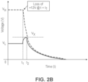
- Fig. 2B shows a diagram of voltage rails after a loss of source power to the circuit of Fig. 2A , according to an embodiment of the invention.
- the diagram shows V H and V L at constant levels until time t 1 .
- Time t 1 may be the point at which switch SW2 in Fig. 2A closes, coupling rail V H to V L through resistor R2. Since V H and V L are now coupled together through R2, capacitors C 1 and C 2 may cause the higher voltage level V H to pull up the voltage level V L as shown until they reach equilibrium voltage level V X at time t 2 .
- the time it takes to from t 1 to t 2 may depend the storage capacitance of C 1 and C 2 , the resistance in resistor R2, and the loads placed on V H and V L , respectively.
- R2 may be sized to make sure that V X does not exceed the maximum voltage of any circuitry powered by V L
- V H and V L may continue to drop in unison until they reach zero volts. In this manner, V H is prevented from dropping below V L throught the powder-down procces. Beyond t 2, with a voltage differential of zero volts, the circuitry of the load may essentially be in the same condition as it is when it has no voltage applied to it, so there should be no problem with damaging voltage differences or with having enough voltage to operate the circuitry in an unknown state.
- V H and V L may drop rapidly, causing the circuitry of the load to see a rapidly decreasing voltage at its power inputs. Since there will not be any revers voltage condition at these inputs, there should not be any damaging voltage conditions.
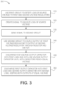
- Fig. 3 shows a flow diagram of a method of operations in the circuitry of Fig. 2A .
- a first circuit may detect a loss of the source voltage that is converted to multiple voltage rails through multiple voltage regulators.At 320 the first circuit may output a signal indicating the source voltage has been lost.
- the first may be sent to a second circuit. In some embodiments the signal may be sent directly. In other embodiments the signal may go through other components before it reaches the second circuit.
- the second circuit may close a switch to connect the first voltage rail to the second voltage rail through a resistor. Due to the resistor connection, at 350 a capacitor connected to the higher voltage rail may discharge into the higher voltage load and may also discharge into a capacitor on the lower voltage rail until both capacitors have the same voltage. At 360, both capacitors may discharge into their respective loads, with their respctive voltages remaining equal. When both capacitors are fully discharged , power-down of the voltage rails may be complete.
- VIN may provide a source voltage for four VRs, labeled VR 1 , VR 2 , VR 3 , and VR 4 , which provide four different voltages to Load 1, Load 2, Load 3, and Load 4, respectively.
- VR 1 may be greater than the output voltage from VR 2 , which is greater than the output voltage of VR 3 , which is greater than the output voltage of VR 4 .
- other configurations may also be used.
- the various Sequence Control circuits (see Fig. 2A ) are indicated as SC XY , where x and y indicate the two VRs whose outputs are connected by that particular Sequence Control circuit.
- the specific outputs that are to be connected in this way may depend on the relative needs of the various loads.
Landscapes
- Engineering & Computer Science (AREA)
- Theoretical Computer Science (AREA)
- Physics & Mathematics (AREA)
- General Physics & Mathematics (AREA)
- General Engineering & Computer Science (AREA)
- Electromagnetism (AREA)
- Radar, Positioning & Navigation (AREA)
- Automation & Control Theory (AREA)
- Power Engineering (AREA)
- Dc-Dc Converters (AREA)
Claims (15)
- Mehrfachspannungserzeugungsschaltung zum Erzeugen mehrerer Spannungsschienen, umfassend:einen ersten Spannungsregler (110) zum Umwandeln einer Eingangsspannung in eine erste Ausgangsspannung an einem ersten Ausgang;einen zweiten Spannungsregler (150) zum Umwandeln der Eingangsspannung in eine zweite Ausgangsspannung an einem zweiten Ausgang, wobei die zweite Ausgangsspannung vor einer ersten Zeit kleiner als die erste Ausgangsspannung sein soll;eine Detektionsschaltung (210) zum Detektieren eines Verlusts der Eingangsspannung und zum Erzeugen eines Signals als Reaktion auf diesen Verlust zu der ersten Zeit; und gekennzeichnet durcheine Sequenzsteuerschaltung (250), die zwischen den ersten Ausgang und den zweiten Ausgang geschaltet ist;wobei die Sequenzsteuerschaltung (250) einen Schalter zum Verbinden des ersten Ausgangs über einen Widerstand mit dem zweiten Ausgang als Reaktion auf das Signal.
- Mehrfachspannungserzeugungsschaltung nach Anspruch 1, wobei die Sequenzsteuerschaltung (250) eine Schottky-Diode in Reihe mit dem Widerstand aufweist.
- Mehrfachspannungserzeugungsschaltung nach Anspruch 1, wobei das Signal den Schalter schließen soll, wenn die Eingangsspannung verloren ist.
- Mehrfachspannungserzeugungsschaltung nach Anspruch 3, ferner umfassend einen ersten Kondensator, der mit dem ersten Ausgang verbunden ist, und einen zweiten Kondensator, der mit dem zweiten Ausgang verbunden ist.
- Mehrfachspannungserzeugungsschaltung nach Anspruch 4, wobei der Schalter bei Empfang des Signals durch die Sequenzsteuerschaltung (250) geschlossen werden soll, um die erste Ausgangsspannung bis zu einer zweiten Zeit größer oder gleich der zweiten Ausgangsspannung zu halten.
- Mehrfachspannungserzeugungsschaltung nach Anspruch 5, wobei der erste Kondensator zwischen dem Schließen des Schalters und der zweiten Zeit in den zweiten Kondensator entladen soll, und nach der zweiten Zeit der erste Kondensator in eine erste Last entladen soll und der zweite Kondensator in eine zweite Last entladen soll.
- Mehrfachspannungserzeugungsschaltung nach Anspruch 1, wobei die Detektionsschaltung (210) eine Diode aufweist, die zwischen einen Eingang des ersten Spannungsreglers (110) und einen Eingang des zweiten Spannungsreglers (150) geschaltet ist.
- System, umfassend:
eine elektronische Vorrichtung (160) mit einem ersten und einem zweiten Lasteingang; und eine Mehrfachspannungserzeugungsschaltung nach Anspruch 1, wobei der erste Ausgang mit dem ersten Lasteingang gekoppelt ist und der zweite Ausgang mit dem zweiten Lasteingang gekoppelt ist. - System nach Anspruch 8, wobei das Signal den Schalter als Reaktion auf die Detektion schließen soll.
- System nach Anspruch 8, wobei das Signal den Schalter schließen soll, wenn die gemeinsame Eingangsspannung verloren ist.
- System nach Anspruch 8, ferner umfassend einen ersten Kondensator, der mit dem ersten Ausgang verbunden ist, und einen zweiten Kondensator, der mit dem zweiten Ausgang verbunden ist.
- System nach Anspruch 11, das derart ausgelegt ist, dass der erste Kondensator in den zweiten Kondensator entladen soll, wenn der Schalter geschlossen ist, bis eine erste Spannung am ersten Ausgang gleich oder größer als eine zweite Spannung am zweiten Ausgang zu einer zweiten Zeit ist.
- System nach Anspruch 12, das derart ausgelegt ist, dass eine Spannung am ersten Kondensator und eine Spannung am zweiten Kondensator nach der zweiten Zeit gleiche Spannungen aufweisen sollen.
- Verfahren zum Betreiben einer Schaltung zum Erzeugen einer ersten und einer zweiten Spannungsschiene, umfassend:Verwenden (310) einer ersten Schaltung zum Detektieren eines Verlusts einer Quellspannung an einen ersten und einen zweiten Spannungsregler;Erzeugung (320) eines Signals als Reaktion auf die Detektion;Senden (330) des Signals an eine zweite Schaltung;Verbinden (340) eines Ausgangs des ersten Spannungsreglers mit einem Ausgang des zweiten Spannungsreglers zu einer ersten Zeit als Reaktion auf den Empfang des Signals durch die zweite Schaltung;wobei das Verbinden Verbinden über einen Widerstand und einen Schalter umfasst.
- Verfahren nach Anspruch 14, wobei das Verbinden Folgendes umfasst:Entladen (350) eines ersten Kondensators am Ausgang des ersten Spannungsreglers in einen zweiten Kondensator am Ausgang des zweiten Spannungsreglers, bis die erste Ausgangsspannung der zweiten Ausgangsspannung zu einer zweiten Zeit entspricht;Aufrechterhalten (350) gleicher Spannungen am ersten und zweiten Kondensator nach der zweiten Zeit; undEntladen (360) des ersten Kondensators in eine erste Last und Entladen des zweiten Kondensators in eine zweite Last nach der zweiten Zeit.
Applications Claiming Priority (2)
| Application Number | Priority Date | Filing Date | Title |
|---|---|---|---|
| US16/225,047 US10908665B2 (en) | 2018-12-19 | 2018-12-19 | Maintaining proper voltage sequence during sudden power loss |
| PCT/US2019/062160 WO2020131278A1 (en) | 2018-12-19 | 2019-11-19 | Maintaining proper voltage sequence during sudden power loss |
Publications (4)
| Publication Number | Publication Date |
|---|---|
| EP3899690A1 EP3899690A1 (de) | 2021-10-27 |
| EP3899690A4 EP3899690A4 (de) | 2022-09-21 |
| EP3899690B1 true EP3899690B1 (de) | 2024-12-18 |
| EP3899690C0 EP3899690C0 (de) | 2024-12-18 |
Family
ID=66243860
Family Applications (1)
| Application Number | Title | Priority Date | Filing Date |
|---|---|---|---|
| EP19898065.8A Active EP3899690B1 (de) | 2018-12-19 | 2019-11-19 | Aufrechterhaltung der richtigen spannungssequenz bei plötzlichem stromausfall |
Country Status (4)
| Country | Link |
|---|---|
| US (1) | US10908665B2 (de) |
| EP (1) | EP3899690B1 (de) |
| PL (1) | PL3899690T3 (de) |
| WO (1) | WO2020131278A1 (de) |
Families Citing this family (2)
| Publication number | Priority date | Publication date | Assignee | Title |
|---|---|---|---|---|
| US10908665B2 (en) * | 2018-12-19 | 2021-02-02 | Intel Corporation | Maintaining proper voltage sequence during sudden power loss |
| US20250251777A1 (en) * | 2024-02-06 | 2025-08-07 | Google Llc | Power sequence control circuit |
Family Cites Families (11)
| Publication number | Priority date | Publication date | Assignee | Title |
|---|---|---|---|---|
| JP2007288974A (ja) | 2006-04-19 | 2007-11-01 | Matsushita Electric Ind Co Ltd | 電源装置及び電源供給方法 |
| JP4345845B2 (ja) * | 2007-05-16 | 2009-10-14 | 株式会社デンソー | 電源装置 |
| US9823719B2 (en) * | 2013-05-31 | 2017-11-21 | Intel Corporation | Controlling power delivery to a processor via a bypass |
| US9564804B2 (en) | 2013-06-28 | 2017-02-07 | Intel Corporation | Electronic device having plurality of voltage rails |
| US9645591B2 (en) | 2014-01-09 | 2017-05-09 | Qualcomm Incorporated | Charge sharing linear voltage regulator |
| US9882383B2 (en) * | 2014-12-23 | 2018-01-30 | Intel Corporation | Smart power delivery network |
| US9857859B2 (en) | 2015-12-21 | 2018-01-02 | Intel Corporation | Techniques to power down output power rails for a storage device |
| US10627839B2 (en) | 2016-03-02 | 2020-04-21 | Qualcomm Incorporated | Multiple input multiple output regulator controller system |
| US10903828B2 (en) * | 2017-04-14 | 2021-01-26 | Intel Corporation | Voltage regulator phase duty cycle control apparatus and method |
| EP3410591B1 (de) * | 2017-06-01 | 2020-03-25 | Vestel Elektronik Sanayi ve Ticaret A.S. | Energiezufuhrsystem und energiezufuhrverfahren |
| US10908665B2 (en) | 2018-12-19 | 2021-02-02 | Intel Corporation | Maintaining proper voltage sequence during sudden power loss |
-
2018
- 2018-12-19 US US16/225,047 patent/US10908665B2/en active Active
-
2019
- 2019-11-19 PL PL19898065.8T patent/PL3899690T3/pl unknown
- 2019-11-19 WO PCT/US2019/062160 patent/WO2020131278A1/en not_active Ceased
- 2019-11-19 EP EP19898065.8A patent/EP3899690B1/de active Active
Also Published As
| Publication number | Publication date |
|---|---|
| EP3899690A4 (de) | 2022-09-21 |
| US10908665B2 (en) | 2021-02-02 |
| PL3899690T3 (pl) | 2025-04-14 |
| WO2020131278A1 (en) | 2020-06-25 |
| EP3899690C0 (de) | 2024-12-18 |
| EP3899690A1 (de) | 2021-10-27 |
| US20190129487A1 (en) | 2019-05-02 |
Similar Documents
| Publication | Publication Date | Title |
|---|---|---|
| CN211086970U (zh) | 一种多电源上下电控制电路 | |
| US6836100B2 (en) | Method and phase redundant regulator apparatus for implementing redundancy at a phase level | |
| US7741820B2 (en) | Switching voltage regulator pulse width modulation controller and method | |
| US5768115A (en) | Voltage booster with an acceleration circuit | |
| US10452113B2 (en) | Power supply switch with programmable switching decision | |
| US8120411B1 (en) | Charge pump with ramp rate control | |
| US20130207695A1 (en) | Power supply circuits with discharge capability and methods of operating same | |
| US7995317B2 (en) | Dual voltage hot swap module power control | |
| US9627962B2 (en) | Fast blocking switch | |
| US7248026B2 (en) | Single-pin tracking/soft-start function with timer control | |
| US8054125B2 (en) | Charge pump with low power, high voltage protection circuitry | |
| US10186961B2 (en) | System and method for output voltage overshoot suppression | |
| US10910820B2 (en) | Fast over voltage and surge detection for high speed and load switches | |
| US9690344B2 (en) | System and method for a power sequencing circuit | |
| EP3899690B1 (de) | Aufrechterhaltung der richtigen spannungssequenz bei plötzlichem stromausfall | |
| DE102018112766A1 (de) | Controllereinrichtung für leistungselektronikschaltung | |
| US10333511B2 (en) | Dual-level power-on reset (POR) circuit | |
| US20110140678A1 (en) | Current limit recovery circuit | |
| US9985431B2 (en) | Bidirectional current limiter | |
| US9343966B1 (en) | Voltage switching system for integrated circuit | |
| JP2006502689A (ja) | 電源制御回路 | |
| CN216052961U (zh) | 一种掉电时序控制电路 | |
| US12132307B2 (en) | Current limiting circuits capable of adjusting current limiting value | |
| US7388356B2 (en) | System and method for providing voltage regulation in a multi-voltage power system | |
| US10158224B1 (en) | Minimizing voltage drop due to current surge at input to a voltage regulator upon turn-on of the voltage regulator |
Legal Events
| Date | Code | Title | Description |
|---|---|---|---|
| STAA | Information on the status of an ep patent application or granted ep patent |
Free format text: STATUS: THE INTERNATIONAL PUBLICATION HAS BEEN MADE |
|
| PUAI | Public reference made under article 153(3) epc to a published international application that has entered the european phase |
Free format text: ORIGINAL CODE: 0009012 |
|
| STAA | Information on the status of an ep patent application or granted ep patent |
Free format text: STATUS: REQUEST FOR EXAMINATION WAS MADE |
|
| 17P | Request for examination filed |
Effective date: 20201214 |
|
| AK | Designated contracting states |
Kind code of ref document: A1 Designated state(s): AL AT BE BG CH CY CZ DE DK EE ES FI FR GB GR HR HU IE IS IT LI LT LU LV MC MK MT NL NO PL PT RO RS SE SI SK SM TR |
|
| DAV | Request for validation of the european patent (deleted) | ||
| DAX | Request for extension of the european patent (deleted) | ||
| A4 | Supplementary search report drawn up and despatched |
Effective date: 20220819 |
|
| RIC1 | Information provided on ipc code assigned before grant |
Ipc: G01R 19/165 20060101ALI20220812BHEP Ipc: G05F 1/569 20060101ALI20220812BHEP Ipc: G06F 1/26 20060101ALI20220812BHEP Ipc: G06F 1/28 20060101ALI20220812BHEP Ipc: G06F 1/30 20060101AFI20220812BHEP |
|
| GRAP | Despatch of communication of intention to grant a patent |
Free format text: ORIGINAL CODE: EPIDOSNIGR1 |
|
| STAA | Information on the status of an ep patent application or granted ep patent |
Free format text: STATUS: GRANT OF PATENT IS INTENDED |
|
| INTG | Intention to grant announced |
Effective date: 20240715 |
|
| GRAS | Grant fee paid |
Free format text: ORIGINAL CODE: EPIDOSNIGR3 |
|
| GRAA | (expected) grant |
Free format text: ORIGINAL CODE: 0009210 |
|
| STAA | Information on the status of an ep patent application or granted ep patent |
Free format text: STATUS: THE PATENT HAS BEEN GRANTED |
|
| AK | Designated contracting states |
Kind code of ref document: B1 Designated state(s): AL AT BE BG CH CY CZ DE DK EE ES FI FR GB GR HR HU IE IS IT LI LT LU LV MC MK MT NL NO PL PT RO RS SE SI SK SM TR |
|
| REG | Reference to a national code |
Ref country code: CH Ref legal event code: EP |
|
| REG | Reference to a national code |
Ref country code: DE Ref legal event code: R096 Ref document number: 602019063814 Country of ref document: DE |
|
| REG | Reference to a national code |
Ref country code: IE Ref legal event code: FG4D |
|
| U01 | Request for unitary effect filed |
Effective date: 20250115 |
|
| U07 | Unitary effect registered |
Designated state(s): AT BE BG DE DK EE FI FR IT LT LU LV MT NL PT RO SE SI Effective date: 20250121 |
|
| PG25 | Lapsed in a contracting state [announced via postgrant information from national office to epo] |
Ref country code: HR Free format text: LAPSE BECAUSE OF FAILURE TO SUBMIT A TRANSLATION OF THE DESCRIPTION OR TO PAY THE FEE WITHIN THE PRESCRIBED TIME-LIMIT Effective date: 20241218 |
|
| PG25 | Lapsed in a contracting state [announced via postgrant information from national office to epo] |
Ref country code: NO Free format text: LAPSE BECAUSE OF FAILURE TO SUBMIT A TRANSLATION OF THE DESCRIPTION OR TO PAY THE FEE WITHIN THE PRESCRIBED TIME-LIMIT Effective date: 20250318 |
|
| PG25 | Lapsed in a contracting state [announced via postgrant information from national office to epo] |
Ref country code: GR Free format text: LAPSE BECAUSE OF FAILURE TO SUBMIT A TRANSLATION OF THE DESCRIPTION OR TO PAY THE FEE WITHIN THE PRESCRIBED TIME-LIMIT Effective date: 20250319 |
|
| PG25 | Lapsed in a contracting state [announced via postgrant information from national office to epo] |
Ref country code: RS Free format text: LAPSE BECAUSE OF FAILURE TO SUBMIT A TRANSLATION OF THE DESCRIPTION OR TO PAY THE FEE WITHIN THE PRESCRIBED TIME-LIMIT Effective date: 20250318 |
|
| PG25 | Lapsed in a contracting state [announced via postgrant information from national office to epo] |
Ref country code: SM Free format text: LAPSE BECAUSE OF FAILURE TO SUBMIT A TRANSLATION OF THE DESCRIPTION OR TO PAY THE FEE WITHIN THE PRESCRIBED TIME-LIMIT Effective date: 20241218 |
|
| PG25 | Lapsed in a contracting state [announced via postgrant information from national office to epo] |
Ref country code: ES Free format text: LAPSE BECAUSE OF FAILURE TO SUBMIT A TRANSLATION OF THE DESCRIPTION OR TO PAY THE FEE WITHIN THE PRESCRIBED TIME-LIMIT Effective date: 20241218 |
|
| PG25 | Lapsed in a contracting state [announced via postgrant information from national office to epo] |
Ref country code: IS Free format text: LAPSE BECAUSE OF FAILURE TO SUBMIT A TRANSLATION OF THE DESCRIPTION OR TO PAY THE FEE WITHIN THE PRESCRIBED TIME-LIMIT Effective date: 20250418 |
|
| PG25 | Lapsed in a contracting state [announced via postgrant information from national office to epo] |
Ref country code: SK Free format text: LAPSE BECAUSE OF FAILURE TO SUBMIT A TRANSLATION OF THE DESCRIPTION OR TO PAY THE FEE WITHIN THE PRESCRIBED TIME-LIMIT Effective date: 20241218 |
|
| PG25 | Lapsed in a contracting state [announced via postgrant information from national office to epo] |
Ref country code: CZ Free format text: LAPSE BECAUSE OF FAILURE TO SUBMIT A TRANSLATION OF THE DESCRIPTION OR TO PAY THE FEE WITHIN THE PRESCRIBED TIME-LIMIT Effective date: 20241218 |
|
| PLBE | No opposition filed within time limit |
Free format text: ORIGINAL CODE: 0009261 |
|
| STAA | Information on the status of an ep patent application or granted ep patent |
Free format text: STATUS: NO OPPOSITION FILED WITHIN TIME LIMIT |
|
| 26N | No opposition filed |
Effective date: 20250919 |
|
| U20 | Renewal fee for the european patent with unitary effect paid |
Year of fee payment: 7 Effective date: 20251023 |
|
| PGFP | Annual fee paid to national office [announced via postgrant information from national office to epo] |
Ref country code: GB Payment date: 20251016 Year of fee payment: 7 |
|
| PGFP | Annual fee paid to national office [announced via postgrant information from national office to epo] |
Ref country code: PL Payment date: 20251029 Year of fee payment: 7 |