EP3893371B1 - Dcdc-wandler - Google Patents
Dcdc-wandler Download PDFInfo
- Publication number
- EP3893371B1 EP3893371B1 EP19907291.9A EP19907291A EP3893371B1 EP 3893371 B1 EP3893371 B1 EP 3893371B1 EP 19907291 A EP19907291 A EP 19907291A EP 3893371 B1 EP3893371 B1 EP 3893371B1
- Authority
- EP
- European Patent Office
- Prior art keywords
- switch
- voltage
- capacitor
- circuit
- inductor
- Prior art date
- Legal status (The legal status is an assumption and is not a legal conclusion. Google has not performed a legal analysis and makes no representation as to the accuracy of the status listed.)
- Active
Links
Images





Classifications
-
- H—ELECTRICITY
- H02—GENERATION; CONVERSION OR DISTRIBUTION OF ELECTRIC POWER
- H02M—APPARATUS FOR CONVERSION BETWEEN AC AND AC, BETWEEN AC AND DC, OR BETWEEN DC AND DC, AND FOR USE WITH MAINS OR SIMILAR POWER SUPPLY SYSTEMS; CONVERSION OF DC OR AC INPUT POWER INTO SURGE OUTPUT POWER; CONTROL OR REGULATION THEREOF
- H02M1/00—Details of apparatus for conversion
- H02M1/0095—Hybrid converter topologies, e.g. NPC mixed with flying capacitor, thyristor converter mixed with MMC or charge pump mixed with buck
-
- H—ELECTRICITY
- H02—GENERATION; CONVERSION OR DISTRIBUTION OF ELECTRIC POWER
- H02M—APPARATUS FOR CONVERSION BETWEEN AC AND AC, BETWEEN AC AND DC, OR BETWEEN DC AND DC, AND FOR USE WITH MAINS OR SIMILAR POWER SUPPLY SYSTEMS; CONVERSION OF DC OR AC INPUT POWER INTO SURGE OUTPUT POWER; CONTROL OR REGULATION THEREOF
- H02M1/00—Details of apparatus for conversion
- H02M1/0048—Circuits or arrangements for reducing losses
- H02M1/0054—Transistor switching losses
-
- H—ELECTRICITY
- H02—GENERATION; CONVERSION OR DISTRIBUTION OF ELECTRIC POWER
- H02M—APPARATUS FOR CONVERSION BETWEEN AC AND AC, BETWEEN AC AND DC, OR BETWEEN DC AND DC, AND FOR USE WITH MAINS OR SIMILAR POWER SUPPLY SYSTEMS; CONVERSION OF DC OR AC INPUT POWER INTO SURGE OUTPUT POWER; CONTROL OR REGULATION THEREOF
- H02M1/00—Details of apparatus for conversion
- H02M1/0083—Converters characterised by their input or output configuration
-
- H—ELECTRICITY
- H02—GENERATION; CONVERSION OR DISTRIBUTION OF ELECTRIC POWER
- H02M—APPARATUS FOR CONVERSION BETWEEN AC AND AC, BETWEEN AC AND DC, OR BETWEEN DC AND DC, AND FOR USE WITH MAINS OR SIMILAR POWER SUPPLY SYSTEMS; CONVERSION OF DC OR AC INPUT POWER INTO SURGE OUTPUT POWER; CONTROL OR REGULATION THEREOF
- H02M3/00—Conversion of DC power input into DC power output
- H02M3/02—Conversion of DC power input into DC power output without intermediate conversion into AC
- H02M3/04—Conversion of DC power input into DC power output without intermediate conversion into AC by static converters
- H02M3/06—Conversion of DC power input into DC power output without intermediate conversion into AC by static converters using resistors or capacitors, e.g. potential divider
- H02M3/07—Conversion of DC power input into DC power output without intermediate conversion into AC by static converters using resistors or capacitors, e.g. potential divider using capacitors charged and discharged alternately by semiconductor devices with control electrode, e.g. charge pumps
-
- H—ELECTRICITY
- H02—GENERATION; CONVERSION OR DISTRIBUTION OF ELECTRIC POWER
- H02M—APPARATUS FOR CONVERSION BETWEEN AC AND AC, BETWEEN AC AND DC, OR BETWEEN DC AND DC, AND FOR USE WITH MAINS OR SIMILAR POWER SUPPLY SYSTEMS; CONVERSION OF DC OR AC INPUT POWER INTO SURGE OUTPUT POWER; CONTROL OR REGULATION THEREOF
- H02M3/00—Conversion of DC power input into DC power output
- H02M3/02—Conversion of DC power input into DC power output without intermediate conversion into AC
- H02M3/04—Conversion of DC power input into DC power output without intermediate conversion into AC by static converters
- H02M3/10—Conversion of DC power input into DC power output without intermediate conversion into AC by static converters using discharge tubes with control electrode or semiconductor devices with control electrode
- H02M3/145—Conversion of DC power input into DC power output without intermediate conversion into AC by static converters using discharge tubes with control electrode or semiconductor devices with control electrode using devices of a triode or transistor type requiring continuous application of a control signal
- H02M3/155—Conversion of DC power input into DC power output without intermediate conversion into AC by static converters using discharge tubes with control electrode or semiconductor devices with control electrode using devices of a triode or transistor type requiring continuous application of a control signal using semiconductor devices only
- H02M3/156—Conversion of DC power input into DC power output without intermediate conversion into AC by static converters using discharge tubes with control electrode or semiconductor devices with control electrode using devices of a triode or transistor type requiring continuous application of a control signal using semiconductor devices only with automatic control of output voltage or current, e.g. switching regulators
- H02M3/158—Conversion of DC power input into DC power output without intermediate conversion into AC by static converters using discharge tubes with control electrode or semiconductor devices with control electrode using devices of a triode or transistor type requiring continuous application of a control signal using semiconductor devices only with automatic control of output voltage or current, e.g. switching regulators including plural semiconductor devices as final control devices for a single load
-
- H—ELECTRICITY
- H02—GENERATION; CONVERSION OR DISTRIBUTION OF ELECTRIC POWER
- H02M—APPARATUS FOR CONVERSION BETWEEN AC AND AC, BETWEEN AC AND DC, OR BETWEEN DC AND DC, AND FOR USE WITH MAINS OR SIMILAR POWER SUPPLY SYSTEMS; CONVERSION OF DC OR AC INPUT POWER INTO SURGE OUTPUT POWER; CONTROL OR REGULATION THEREOF
- H02M3/00—Conversion of DC power input into DC power output
- H02M3/02—Conversion of DC power input into DC power output without intermediate conversion into AC
- H02M3/04—Conversion of DC power input into DC power output without intermediate conversion into AC by static converters
- H02M3/06—Conversion of DC power input into DC power output without intermediate conversion into AC by static converters using resistors or capacitors, e.g. potential divider
- H02M3/07—Conversion of DC power input into DC power output without intermediate conversion into AC by static converters using resistors or capacitors, e.g. potential divider using capacitors charged and discharged alternately by semiconductor devices with control electrode, e.g. charge pumps
- H02M3/072—Conversion of DC power input into DC power output without intermediate conversion into AC by static converters using resistors or capacitors, e.g. potential divider using capacitors charged and discharged alternately by semiconductor devices with control electrode, e.g. charge pumps adapted to generate an output voltage whose value is lower than the input voltage
-
- H—ELECTRICITY
- H02—GENERATION; CONVERSION OR DISTRIBUTION OF ELECTRIC POWER
- H02M—APPARATUS FOR CONVERSION BETWEEN AC AND AC, BETWEEN AC AND DC, OR BETWEEN DC AND DC, AND FOR USE WITH MAINS OR SIMILAR POWER SUPPLY SYSTEMS; CONVERSION OF DC OR AC INPUT POWER INTO SURGE OUTPUT POWER; CONTROL OR REGULATION THEREOF
- H02M3/00—Conversion of DC power input into DC power output
- H02M3/02—Conversion of DC power input into DC power output without intermediate conversion into AC
- H02M3/04—Conversion of DC power input into DC power output without intermediate conversion into AC by static converters
- H02M3/10—Conversion of DC power input into DC power output without intermediate conversion into AC by static converters using discharge tubes with control electrode or semiconductor devices with control electrode
- H02M3/145—Conversion of DC power input into DC power output without intermediate conversion into AC by static converters using discharge tubes with control electrode or semiconductor devices with control electrode using devices of a triode or transistor type requiring continuous application of a control signal
- H02M3/155—Conversion of DC power input into DC power output without intermediate conversion into AC by static converters using discharge tubes with control electrode or semiconductor devices with control electrode using devices of a triode or transistor type requiring continuous application of a control signal using semiconductor devices only
- H02M3/156—Conversion of DC power input into DC power output without intermediate conversion into AC by static converters using discharge tubes with control electrode or semiconductor devices with control electrode using devices of a triode or transistor type requiring continuous application of a control signal using semiconductor devices only with automatic control of output voltage or current, e.g. switching regulators
- H02M3/1566—Conversion of DC power input into DC power output without intermediate conversion into AC by static converters using discharge tubes with control electrode or semiconductor devices with control electrode using devices of a triode or transistor type requiring continuous application of a control signal using semiconductor devices only with automatic control of output voltage or current, e.g. switching regulators with means for compensating against rapid load changes, e.g. with auxiliary current source, with dual mode control or with inductance variation
-
- H—ELECTRICITY
- H02—GENERATION; CONVERSION OR DISTRIBUTION OF ELECTRIC POWER
- H02M—APPARATUS FOR CONVERSION BETWEEN AC AND AC, BETWEEN AC AND DC, OR BETWEEN DC AND DC, AND FOR USE WITH MAINS OR SIMILAR POWER SUPPLY SYSTEMS; CONVERSION OF DC OR AC INPUT POWER INTO SURGE OUTPUT POWER; CONTROL OR REGULATION THEREOF
- H02M7/00—Conversion of AC power input into DC power output; Conversion of DC power input into AC power output
- H02M7/42—Conversion of DC power input into AC power output without possibility of reversal
- H02M7/44—Conversion of DC power input into AC power output without possibility of reversal by static converters
- H02M7/48—Conversion of DC power input into AC power output without possibility of reversal by static converters using discharge tubes with control electrode or semiconductor devices with control electrode
- H02M7/483—Converters with outputs that each can have more than two voltages levels
- H02M7/4837—Flying capacitor converters
-
- Y—GENERAL TAGGING OF NEW TECHNOLOGICAL DEVELOPMENTS; GENERAL TAGGING OF CROSS-SECTIONAL TECHNOLOGIES SPANNING OVER SEVERAL SECTIONS OF THE IPC; TECHNICAL SUBJECTS COVERED BY FORMER USPC CROSS-REFERENCE ART COLLECTIONS [XRACs] AND DIGESTS
- Y02—TECHNOLOGIES OR APPLICATIONS FOR MITIGATION OR ADAPTATION AGAINST CLIMATE CHANGE
- Y02B—CLIMATE CHANGE MITIGATION TECHNOLOGIES RELATED TO BUILDINGS, e.g. HOUSING, HOUSE APPLIANCES OR RELATED END-USER APPLICATIONS
- Y02B70/00—Technologies for an efficient end-user side electric power management and consumption
- Y02B70/10—Technologies improving the efficiency by using switched-mode power supplies [SMPS], i.e. efficient power electronics conversion e.g. power factor correction or reduction of losses in power supplies or efficient standby modes
Definitions
- Embodiments of this application relate to direct current-direct current technologies, and in particular, to a DC-DC converter.
- a direct current-direct current (DC-DC) converter is a common voltage converter.
- the DC-DC converter may implement buck, boost, buck-boost, and the like.
- DC-DC converters that can implement a buck function include a buck converter implemented by using an inductor, an SC converter implemented by using a switched capacitor (SC), and a three-order hybrid converter implemented by using an inductor and a capacitor.
- SC switched capacitor
- the DC-DC converters described above have poor voltage conversion efficiency and poor transient performance.
- US2008/239772 discloses a switched capacitor converter according to the preamble of claim 1.
- US2014/184189 discloses a similar DC-DC converter adapted for converting a plurality of input voltages to a plurality of output voltages.
- US 2016/344214 A1 discloses a voltage or current regulated power converter for charging batteries, is described.
- the power converter comprises an inductor, a capacitor cell, switches and a controller.
- the controller controls the switches such that a commutation cycle of the power converter comprises a first phase, during which the capacitor cell and the inductor are arranged in series and during which a voltage across the serial arrangement of the capacitor cell and the inductor corresponds to V in -V out ; a second phase, during which the capacitor cell and the inductor are arranged in series and during which the voltage across the serial arrangement of the capacitor cell and the inductor corresponds to -V out ; and a third phase, during which the capacitor cell is floating and during which the voltage across the inductor corresponds to V in -V out or to -V out .
- LIYONGJUN ET AL "An AC-coupled stacked dual active bridge hybrid DC-DC converter for battery-to-processor power delivery with 87.2% peak efficiency and high accuracy loadline regulation", 2018 IEEE CUSTOM INTEGRATED CIRCUITS CONFERENCE (CICC), IEEE, 8 April 2018 (2018-04-08), pages 1-4 , discloses a 3-phase AC-coupled stacked DAB DC-DC converter topology.
- the converter can operate under a common Li-ion battery voltage of 3.2V-4.2V and achieve continuous output regulation of 0.8V-1.5V.
- Embodiments of this application provide a direct current-direct current DC-DC converter, to improve transient performance while providing voltage conversion efficiency.
- the invention is defined by a DC-DC converter according to claim 1.
- the DC-DC converter is configured to receive input voltage from a voltage input end, and output voltage to a voltage output end.
- the DC-DC converter includes a first capacitor, a second capacitor, a switched capacitor SC circuit, and an inductor circuit.
- An input end of the SC circuit is coupled to the voltage input end, and an output end of the SC circuit is coupled to the voltage output end.
- the first capacitor and the second capacitor are sequentially connected in series between the voltage input end and the voltage output end.
- One end of the inductor circuit is selectively coupled between the first capacitor and the second capacitor or to a ground end, and the other end of the inductor circuit is coupled to the voltage output end.
- the SC circuit works in an open-loop mode, and voltage conversion efficiency is relatively high.
- the output voltage at the voltage output end is adjusted by a buck structure implemented by using the inductor circuit, so that transient performance of the DC-DC converter can be ensured.
- the DC-DC converter has high voltage conversion efficiency and good transient performance.
- the SC circuit includes a third capacitor and a fourth capacitor.
- One end of the third capacitor is selectively coupled to the voltage input end or the voltage output end, and the other end of the third capacitor is selectively coupled to the voltage output end or the ground end.
- One end of the fourth capacitor is selectively coupled to the voltage input end or the voltage output end, and the other end of the fourth capacitor is selectively coupled between the first capacitor and the second capacitor or to the ground end.
- the DC-DC converter provided in this embodiment has high voltage conversion efficiency and good transient performance.
- the SC circuit further includes a first switch, a second switch, a third switch, a fourth switch, a fifth switch, a sixth switch, and a seventh switch.
- a first end of the first switch is coupled to the ground end
- a first end of the second switch is coupled to the voltage output end
- a second end of the first switch is coupled to a first end of the third capacitor
- a second end of the second switch is coupled to the first end of the third capacitor.
- a first end of the third switch is coupled to the ground end
- a first end of the fourth switch is coupled to a second end of the first capacitor
- a second end of the third switch is coupled to a first end of the fourth capacitor
- a second end of the fourth switch is coupled to the first end of the fourth capacitor.
- a second end of the third capacitor is coupled to a first end of the fifth switch, a second end of the fifth switch is coupled to the voltage output end, a second end of the fourth capacitor is coupled to a first end of the sixth switch, and a second end of the sixth switch is coupled to the first end of the fifth switch.
- a first end of the seventh switch is coupled to the voltage input end, and a second end of the seventh switch is coupled to the second end of the fourth capacitor.
- a first end of the first capacitor is coupled to the voltage input end, the second end of the first capacitor is coupled to a first end of the second capacitor, and a second end of the second capacitor is coupled to the ground end.
- the SC circuit is implemented by using a 2:1 SC circuit, and the DC-DC converter is further obtained based on the SC circuit and the inductor circuit, so as to implement a DC-DC converter that improves transient performance while improving voltage conversion efficiency.
- the inductor circuit includes an inductor.
- a first end of the eighth switch is coupled to the first end of the second capacitor, a second end of the eighth switch is coupled to a first end of the ninth switch, a second end of the ninth switch is coupled to the ground end, a first end of the inductor is coupled to the first end of the ninth switch, and a second end of the inductor is coupled to the voltage output end.
- the output voltage at the voltage output end of the DC-DC converter is adjusted by using the inductor circuit, so as to implement a DC-DC converter that improves transient performance while improving voltage conversion efficiency.
- the DC-DC converter provided in the embodiments of this application includes the first capacitor, the second capacitor, the switched capacitor SC circuit, and the inductor circuit.
- the input end of the SC circuit is coupled to the voltage input end, and the output end of the SC circuit is coupled to the voltage output end.
- the first capacitor and the second capacitor are sequentially connected in series between the voltage input end and the voltage output end.
- One end of the inductor circuit is selectively coupled between the first capacitor and the second capacitor or to the ground end, and the other end of the inductor circuit is coupled to the voltage output end.
- the SC circuit works in an open-loop mode, and voltage conversion efficiency is relatively high.
- the output voltage at the voltage output end is adjusted by a buck structure implemented by using the inductor circuit, so that transient performance of the DC-DC converter can be ensured.
- the DC-DC converter has high voltage conversion efficiency and good transient performance.
- conventional DC-DC converters that can implement a buck function include a buck converter implemented by using an inductor, an SC converter implemented by using a capacitor, and a three-order hybrid (hybrid) converter implemented by using an inductor and a capacitor.
- the three converters are separately described below in detail. For example, reference may be made to FIG. 1A , FIG. 1B , FIG. 1C , and FIG. 1D .
- FIG. 1A is a circuit of a buck converter implemented by using an inductor.
- a P-type metal-oxide semiconductor p-type metal-oxide semiconductor, PMOS
- an N-type metal-oxide semiconductor n-type metal-oxide semiconductor, NMOS
- input voltage VDD is connected to the PMOS.
- the PMOS and the NMOS are alternately turned on and turned off under driving of a PG signal and an NG signal provided by a drive circuit.
- An alternating-current signal that is output at an output node LX is used to enable an inductor L to store energy, so as to provide direct-current output voltage VO to two ends of a capacitor.
- a load resistor connected to the output end is connected to the drive circuit to form a closed-loop feedback, and consequently the inductor has a magnetic loss.
- FIG. 1B is an SC converter implemented by using a capacitor.
- a switch M1 and a switch M4 are turned on, a switch M2 and a switch M3 are turned off, and input voltage VDD directly charges a fly capacitor C F and an output capacitor C L .
- the switch M1 and the switch M4 are turned off, the switch M2 and the switch M3 are turned on, the fly capacitor C F and the output capacitor C L are connected in parallel, and the fly capacitor C F discharges electricity to the output capacitor C L .
- the SC converter works in an open-loop state, and voltage between two ends of the non-capacitor C F is VO. VO is about half of the input voltage VDD.
- the SC converter works in a closed-loop state, it is difficult to improve overall conversion efficiency because a conductive impedance of a switch tube in a channel needs to be adjusted. Therefore, the SC converter usually works in an open-loop state, and theoretical conversion efficiency may be close to 100%, but overall transient performance is relatively poor because there is no loop adjustment feature.
- FIG. 1C is a schematic module diagram of a hybrid converter
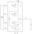
- FIG. 1D is a circuit of a hybrid converter
- the hybrid converter includes a high-efficiency SC architecture implemented by using a capacitor and a buck structure implemented by using an inductor, and the SC architecture and the buck architecture are connected in series.
- the hybrid converter includes two PMOSs and two NMOSs, which are respectively P1, P2, N1, and N2 shown in the figure.
- a drive circuit is configured to provide a PG1, a PG2, an NG1, and an NG2, which are respectively used to control P1, P2, N1, and N2 to be turned on and turned off.
- the PG1 is connected to input voltage VDD.
- a 1/4 period P1 and N2 are turned on, and P2 and N1 are turned off, VDD supplies power to an output end by using a fly capacitor C F and an inductor L.
- N1 and N2 are turned on, P1 and P2 are turned off, and power is supplied to the output end by using the ground and the inductor L.
- P1 and N2 are turned off, P2 and N1 are turned on, and the fly capacitor C F supplies power to the output end by using the inductor L.
- N1 and N2 are turned on, P1 and P2 are turned off, and energy is provided to the output end by using the ground and the inductor L.
- embodiments of this application provide a direct current-direct current DC-DC converter, to improve transient performance while providing voltage conversion efficiency.
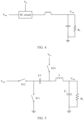
- FIG. 2 is a schematic structural diagram of a DC-DC converter according to an embodiment of this application.
- the DC-DC converter provided in this embodiment of this application is configured to receive input voltage from a voltage input end, and output voltage to a voltage output end.
- the DC-DC converter includes a first capacitor C1, a second capacitor C2, an SC circuit, and an inductor circuit.
- An input end of the SC circuit is coupled to the voltage input end, and an output end of the SC circuit is coupled to the voltage output end.
- the first capacitor C1 and the second capacitor C2 are sequentially connected in series between the voltage input end and the voltage output end.
- One end of the inductor circuit is selectively coupled between the first capacitor and the second capacitor or to a ground end, and the other end of the inductor circuit is coupled to the voltage output end.
- the SC circuit works in an open-loop mode, and the inductor circuit including an inductor works in a closed-loop mode.
- the DC-DC converter provided in this embodiment of this application includes the first capacitor, the second capacitor, the switched capacitor SC circuit, and the inductor circuit.
- the input end of the SC circuit is coupled to the voltage input end, and the output end of the SC circuit is coupled to the voltage output end.
- the first capacitor and the second capacitor are sequentially connected in series between the voltage input end and the voltage output end.
- One end of the inductor circuit is selectively coupled between the first capacitor and the second capacitor or to the ground end, and the other end of the inductor circuit is coupled to the voltage output end.
- the SC circuit works in an open-loop mode, and voltage conversion efficiency is relatively high.
- the output voltage at the voltage output end is adjusted by a buck structure implemented by using the inductor circuit, so that transient performance of the DC-DC converter can be ensured.
- the DC-DC converter has high voltage conversion efficiency and good transient performance.
- the SC circuit includes a third capacitor C3 and a fourth capacitor C4.
- One end of the third capacitor is selectively coupled to the voltage input end or the voltage output end, and the other end of the third capacitor C3 is selectively coupled to the voltage output end or the ground end.
- One end of the fourth capacitor C4 is selectively coupled to the voltage input end or the voltage output end, and the other end of the fourth capacitor C4 is selectively coupled between the first capacitor C1 and the second capacitor C2 or to the ground end.
- FIG. 3 is a circuit diagram of another DC-DC converter according to an embodiment of this application.
- the SC circuit includes a first switch S1, a second switch S2, a third switch S3, a fourth switch S4, a fifth switch S5, a sixth switch S6, a seventh switch S7, a third capacitor C3, and a fourth capacitor C4.
- a first end of the first switch S1 is coupled to the ground end
- a first end of the second switch S2 is coupled to the voltage output end
- a second end of the first switch S1 is coupled to a first end of the third capacitor C3, and a second end of the second switch S2 is coupled to the first end of the third capacitor C3.
- a first end of the third switch S3 is coupled to the ground end, a first end of the fourth switch S4 is coupled to a second end of the first capacitor C1, a second end of the third switch S3 is coupled to a first end of the fourth capacitor C4, a second end of the fourth switch S4 is coupled to the first end of the fourth capacitor C4.
- a second end of the third capacitor C3 is coupled to a first end of the fifth switch S5, a second end of the fifth switch S5 is coupled to the voltage output end, a second end of the fourth capacitor C4 is coupled to a first end of the sixth switch S6, a second end of the sixth switch S6 is coupled to the first end of the fifth switch S5, a first end of the seventh switch S7 is coupled to the voltage input end, and a second end of the seventh switch S7 is coupled to the second end of the fourth capacitor C4.
- a first end of the first capacitor C1 is coupled to the voltage input end
- the second end of the first capacitor C1 is coupled to a first end of the second capacitor C2
- a second end of the second capacitor C2 is coupled to the ground end.
- the DC-DC converter implements voltage conversion in which the input voltage Vin at the voltage input end is converted to the output voltage Vout at the voltage output end.
- the DC-DC converter provided in this embodiment is applied to a scenario in which a duty cycle of output-input conversion is less than 50%.
- a working principle is as follows:
- the SC circuit is a 2:1 SC circuit, and the 2:1 SC circuit includes the first switch S1, the second switch S2, the third switch S3, the fifth switch S5, the sixth switch S6, and the third capacitor C3.
- the inductor circuit works in a closed-loop mode, and the SC circuit works in an open-loop mode.
- Input voltage of the SC circuit and that of the inductor circuit are connected in series to the voltage input end, and voltage output ends of the SC circuit and the inductor circuit both are coupled to the voltage output end.
- the first switch S1, the fourth switch S4, the fifth switch S5, and the seventh switch S7 are turned on, and the second switch S2, the third switch S3, and the sixth switch S6 are turned off.
- a charge on the first capacitor C1 is directly discharged to the fourth capacitor C4, the fourth capacitor C4 is in a charging state, the third capacitor C3 discharges energy to the voltage output end, and the third capacitor C3 discharges.
- the first switch S1, the fourth switch S4, the fifth switch S5, and the seventh switch S7 are turned off, and the second switch S2, the third switch S3, and the sixth switch S6 are turned on.
- the third capacitor C3 and the fourth capacitor C4 are connected in series and are coupled to the voltage output end, energy of the fourth capacitor C4 is directly discharged to the voltage output end by using the third capacitor C3, the fourth capacitor C4 discharges energy, and the third capacitor C3 stores energy.
- the SC circuit is implemented by using a 2:1 SC circuit, and the DC-DC converter is further obtained based on the SC circuit and the inductor circuit, so as to implement a DC-DC converter that improves transient performance while improving voltage conversion efficiency.
- the inductor circuit includes an eighth switch S8, a ninth switch S9, and an inductor L.
- a first end of the eighth switch S8 is coupled to the first end of the second capacitor C2
- a second end of the eighth switch S8 is coupled to a first end of the ninth switch S9
- a second end of the ninth switch S9 is coupled to the ground end
- a first end of the inductor L is coupled to the first end of the ninth switch S9
- a second end of the inductor L is coupled to the voltage output end.
- Vmid is an input power supply of the inductor circuit
- the eighth switch S8 and the ninth switch S9 are alternately turned on or turned off.
- the eighth switch S8 and the ninth switch S9 are independent of statuses of the first switch S1, the second switch S2, the third switch S3, the fourth switch S4, the fifth switch S5, the sixth switch S6, and the seventh switch S7.
- the inductor circuit In a working process of the DC-DC converter, based on the inductor circuit, when the output voltage Vout at the voltage output end is lower than the target voltage, the inductor circuit begins to perform adjustment to prolong on duration of the eighth switch S8 and shorten on duration of the ninth switch S9, so that a current drawn from the voltage end Vmid becomes larger. After the current is drawn, the voltage Vmid is decreased, and in this case, the input voltage V1 of the SC circuit is increased. In addition, because the SC circuit works in an open-loop state, the SC circuit provides energy to the voltage output end, thereby increasing the output voltage at the voltage output end.
- the inductor circuit performs reverse adjustment, that is, shortens the on duration of the eighth switch S8 and prolongs the on duration of the ninth switch S9, so that a current drawn from the voltage output end becomes smaller.
- the voltage Vmid is increased, and voltage between the two ends of the first capacitor C1 is decreased, and the output voltage Vout at the voltage output end is decreased.
- Voltage conversion efficiency of the DC-DC converter shown in FIG. 3 is better than voltage conversion efficiency of a conventional DC-DC converter, because the SC circuit works in an open-loop mode, and there is no magnetic loss of an inductor of a conventional DC-DC converter implemented by using the inductor and no switch overlapping loss of a power tube.
- efficiency of conversion from V1 to Vout can easily be over 90%, or even may be over 95%. It is assumed that conversion efficiency of the SC circuit is ⁇ SC .
- a proportion of conversion in which the input voltage is decreased from Vin to V2 is much smaller.
- the inductor circuit in this embodiment of this application has a lower magnetic loss.
- switch losses of the eighth switch S8 and the ninth switch S9 in this embodiment of this application are lower than those of a PMOS and an NMOS in the conventional DC-DC converter implemented by using an inductor.
- the eighth switch S8 and the ninth switch S9 may be switch tubes with a low withstand voltage. A figure of merit (figure of merit, FOM) value is smaller, and a related loss also becomes smaller.
- the inductor circuit including the eighth switch S8, the ninth switch S9, and the inductor L implements voltage conversion from V2 to the output voltage Vout.
- Vout/V1 Compared with voltage conversion directly from the input voltage Vin to the output voltage Vout, a value of Vout/V1 is greater than a value of Vout/Vin, and therefore voltage conversion efficiency is high.
- conversion efficiency of the inductor circuit is ⁇ bk
- conversion efficiency of the DC-DC converter is ⁇ SC ⁇ V 1 + ⁇ bk ⁇ V 2 V 1 + V 2 . Because both ⁇ SC and ⁇ bk are higher than efficiency of conventional conversion from Vin to Vout, the DC-DC converter has high voltage conversion efficiency.
- the output voltage at the voltage output end of the DC-DC converter is adjusted by using the inductor circuit, so as to implement a DC-DC converter that improves transient performance while improving voltage conversion efficiency.
- the inductor circuit adjusts the output voltage at the voltage output end in the foregoing embodiment is described below in detail.
- the on duration of the eighth switch is prolonged, so that the SC circuit reaches a stable state.
- the on duration of the ninth switch is prolonged, so that the SC circuit reaches a stable state.
- the eighth switch S8 and the ninth switch S9 are alternately turned on or turned off.
- the on duration of the eighth switch S8 is prolonged, and the on duration of the ninth switch S9 is shortened, so that the SC circuit reaches a stable state.
- the on duration of the ninth switch S9 is prolonged, and the on duration of the eighth switch S8 is shortened, so that the SC circuit reaches a stable state.
- duration of a period is 10 seconds.
- duration in which the eighth switch S8 is turned on and the ninth switch S9 is turned off is 5 seconds
- duration in which the eighth switch S8 is turned off and the ninth switch S9 is turned on is 5 seconds.
- the on duration of the eighth switch S8 is prolonged to 7 seconds
- the on duration of the ninth switch S9 is shortened to 3 seconds. In this case, because the on duration of the eighth switch S8 is prolonged, energy provided by the inductor circuit to the voltage output end is also increased. Therefore, the output voltage at the voltage output end can be increased.
- the current drawn from Vmid is also increased, the voltage at Vmid is decreased, and the voltage between the two ends of the first capacitor C1 is increased, so that the input voltage of the SC circuit is increased, and the output voltage at the SC circuit is inevitably increased. It may be learned from this that both the output voltage of the SC circuit and the output voltage of the inductor circuit are increased. In addition, the output ends of the SC circuit and the inductor circuit both are coupled to the voltage output end, and therefore the output voltage at the voltage output end is inevitably increased. When the output voltage at the voltage output end is higher than the target voltage, the on duration of the eighth switch S8 is shortened to 4 seconds, and the on duration of the ninth switch S9 is prolonged to 6 seconds.
- the on duration of the eighth switch and that of the ninth switch in the inductor circuit are adjusted, so as to adjust the output voltage at the voltage output end of the DC-DC converter.
- FIG. 4 is a structural diagram of still another DC-DC converter according to an embodiment of this application.
- the DC-DC converter is configured to receive input voltage from a voltage input end, and output voltage to a voltage output end.
- the DC-DC converter includes a switched capacitor SC circuit and an inductor.
- An input end of the SC circuit is coupled to the voltage input end.
- Output ends of the SC circuit include a first output end and a second output end. The first output end is coupled to the voltage output end, the second output end is coupled to one end of the inductor, and the other end of the inductor is coupled to an output end.
- a capacitor included in the SC circuit is selectively adjusted to be connected in parallel or in series to the inductor.
- the DC-DC converter works, and the SC circuit is in an energy storage state or an energy discharging state, the SC circuit and the inductor are connected in parallel.
- the SC circuit and the inductor are connected in parallel, because the SC circuit is configured to improve voltage conversion efficiency, and the inductor is configured to improve transient performance, conversion efficiency of the DC-DC converter is equal to the sum of conversion efficiency of the SC circuit and conversion efficiency of the inductor, instead of conversion efficiency of a conventional hybrid DC-DC converter that is equal to a product of the conversion efficiency of the SC circuit and the conversion efficiency of the inductor. Therefore, the DC-DC converter provided in this embodiment of this application can improve voltage conversion efficiency.
- the DC-DC converter in FIG. 4 is described below in detail by using two examples. For example, reference may be made to FIG. 5 and FIG. 6 .
- FIG. 5 is a structural diagram of still another DC-DC converter.
- the capacitor included in the SC circuit is a fifth capacitor C5
- the SC circuit further includes a tenth switch S10, an eleventh switch S11, and a twelfth switch S12.
- a first end of the tenth switch S10 is coupled to the voltage input end, a second end of the tenth switch S10 is coupled to a first end of the fifth capacitor C5, a second end of the fifth capacitor C5 is coupled to a first end of the eleventh switch S11, a second end of the eleventh switch S11 is coupled to a ground end, the first end of the eleventh switch S11 is coupled to a first end of the twelfth switch S12, a second end of the twelfth switch S12 is coupled to the voltage output end, the first end of the fifth capacitor C5 is coupled to a first end of the inductor L, and a second end of the inductor L is coupled to the voltage output end.
- the voltage output end is connected to a load capacitor C L , a load resistor R L , or the like.
- the SC circuit included in the DC-DC converter is an open-loop SC architecture, and a buck circuit including the inductor L works in a closed-loop mode.
- the DC-DC converter provided in this embodiment is applied to a scenario in which a duty cycle of output-input conversion is greater than 50%.
- a working principle is as follows: When the tenth switch S10 and the twelfth switch S12 are turned on, and the eleventh switch S11 is turned off, in one aspect, the voltage input end provides energy to the voltage output end by using the inductor L, and a current direction is from the voltage input end to the inductor L and then to the voltage output end.
- the voltage input end charges the fifth capacitor C5 while providing energy to the voltage output end by using the fifth capacitor C5, and a current direction is from the voltage input end to the fifth capacitor C5 and then to the voltage output end.
- the SC circuit is an open-loop SC architecture, a switch voltage drop of the SC circuit is smaller than that of a power supply, and conversion efficiency of the entire SC is relatively high.
- the SC works in an open-loop state, and voltage drops at the two ends of the inductor L are relatively small, so that a magnetic loss of the inductor L is relatively small. Therefore, conversion efficiency of the DC-DC converter is relatively high overall.
- the tenth switch S10 and the twelfth switch S12 are in an open state, which is equivalent to that the input voltage at the voltage input end is turned off and that only the fifth capacitor C5 provides energy to the voltage output end by using the inductor L. Therefore, the output voltage at the voltage output end can be decreased, and the SC circuit reaches a stable state.
- voltage between the two ends of the fifth capacitor C5 is the same as the output voltage at the voltage output end.
- the on duration of the switch in the DCDC circuit is adjusted, so as to adjust the output voltage at the voltage output end of the DC-DC converter.
- the SC circuit may further include another switch.
- the switch is disposed between the tenth switch S10 and the inductor L, that is, between the fifth capacitor C5 and the inductor L.
- the switch may be omitted due to existence of the inductor L, so that the SC circuit includes only the tenth switch S10, the eleventh switch S11, the twelfth switch S12, and the fifth capacitor C5.
- FIG. 6 is a structural diagram of still another DC-DC converter.
- the capacitor included in the SC circuit is a sixth capacitor, and the SC circuit further includes a thirteenth switch S13, a fourteenth switch S14, and a fifteenth switch S15.
- a first end of the thirteenth switch S13 is coupled to the voltage output end, a second end of the thirteenth switch S13 is coupled to a first end of the sixth capacitor C6, a second end of the sixth capacitor C6 is coupled to a first end of the fourteenth switch S14, a second end of the fourteenth switch S14 is coupled to a ground end, the first end of the sixth capacitor C6 is coupled to a first end of the fifteenth switch S15, a second end of the fifteenth switch S15 is coupled to an output end, the second end of the sixth capacitor C6 is coupled to a first end of the inductor L, and a second end of the inductor L is coupled to the voltage output end.
- the voltage output end is connected to a load capacitor CL, a load resistor RL, or the like.
- the SC circuit included in the DC-DC converter is an open-loop SC architecture.
- the DC-DC converter provided in this embodiment is applied to a scenario in which a duty cycle of output-input conversion is less than 50%.
- a working principle is as follows: When the thirteenth switch S13 is turned on, and the fourteenth switch S14 and the fifteenth switch S15 are turned off, the voltage input end provides energy to the voltage output end by using the sixth capacitor C6 and the inductor L. In this case, the sixth capacitor C6 is in a charging state, and a current flows from the voltage input end to the voltage output end through the thirteenth switch S13, the sixth capacitor C6, and the inductor L.
- the inductor L provides energy to the voltage output end.
- the sixth capacitor C6 provides energy to the voltage output end by using the fifteenth switch S15, and the sixth capacitor C6 is in a discharging state.
- Vc Vout.
- the SC circuit works in an open-loop mode, a switch voltage drop of the SC circuit is smaller than that of a power supply, and conversion efficiency of the entire SC is relatively high.
- the SC works in an open-loop state, and voltage drops at the two ends of the inductor L are relatively small, so that a magnetic loss of the inductor L is relatively small. Therefore, conversion efficiency of the DC-DC converter is relatively high overall.
- FIG. 7 is a schematic diagram of a relationship between a high-transient module and a high-efficiency module when the SC circuit in FIG. 6 is in an energy discharging state.
- conversion efficiency of the DC-DC converter is the sum of conversion efficiency of the SC circuit and conversion efficiency of a buck circuit formed by using the inductor, instead of conversion efficiency of a conventional hybrid DC-DC converter that is equal to a product of the conversion efficiency of the SC circuit and the conversion efficiency of the inductor. Therefore, the DC-DC converter provided in this embodiment of this application can improve voltage conversion efficiency.
- the DC-DC converter provided in this embodiment of this application can improve transient performance while improving voltage conversion efficiency.
- the SC circuit may further include another switch.
- the switch is disposed between the fourteenth switch S 14 and the inductor L, that is, between the sixth capacitor C6 and the inductor L.
- the switch may be omitted due to existence of the inductor L, so that the SC circuit includes only the thirteenth switch S13, the fourteenth switch S14, the fifteenth switch S15, and the sixth capacitor C6.
Landscapes
- Engineering & Computer Science (AREA)
- Power Engineering (AREA)
- Dc-Dc Converters (AREA)
Claims (3)
- Gleichstrom-Gleichstrom-Wandler, ausgelegt zum Empfangen einer Eingangsspannung von einem Spannungseingangsende und zum Bereitstellen einer Ausgangsspannung an einem Spannungsausgangsende, wobei der Gleichstrom-Gleichstrom-Wandler einen ersten Kondensator (C1), einen zweiten Kondensator (C2), eine Switched-Capacitor- bzw. SC-Schaltung und eine Induktivitätsschaltung umfasst, ein Eingangsende der SC-Schaltung mit dem Spannungseingangsende gekoppelt ist und ein Ausgangsende der SC-Schaltung mit dem Spannungsausgangsende gekoppelt ist; der erste Kondensator (C1) und der zweite Kondensator (C2) zwischen dem Spannungseingangsende und einem Masseende in Reihe geschaltet sind, ein Ende der Induktivitätsschaltung selektiv entweder mittels eines achten Schalters (S8) mit einem Mittelpunkt des ersten Kondensators (C1) und des zweiten Kondensators (C2) oder mittels eines neunten Schalters (S9) mit dem Masseende verbindbar ist und das andere Ende der Induktivitätsschaltung mit dem Spannungsausgangsende gekoppelt ist,
wobei die SC-Schaltung einen dritten Kondensator (C3) und einen vierten Kondensator (C4) umfasst, ein erstes Ende des dritten Kondensators (C3) selektiv entweder mittels eines sechsten Schalters (S6) mit einem ersten Ende des vierten Kondensators (C4) oder mittels eines fünften Schalters (S5) mit dem Spannungsausgangsende verbindbar ist und das andere Ende des dritten Kondensators (C3) selektiv entweder mittels eines zweiten Schalters (S2) mit dem Spannungsausgangsende oder mittels eines ersten Schalters (S1) mit dem Masseende verbindbar ist, das erste Ende des vierten Kondensators (C4) selektiv entweder mittels eines siebten Schalters (S7) mit dem Spannungseingangsende oder mittels des sechsten Schalters (S6) mit dem ersten Ende des dritten Kondensators (C3) verbindbar ist und das andere Ende des vierten Kondensators (C4) selektiv entweder mittels eines vierten Schalters (S4) mit dem Mittelpunkt des ersten Kondensators (C1) und des zweiten Kondensators (C2) oder mittels eines dritten Schalters (S3) mit dem Masseende verbindbar ist und wobei der Gleichstrom-Gleichstrom-Wandler ausgelegt ist zum Implementieren eines Modus offener Schleife für die SC-Schaltung mit den folgenden zwei Zuständen:Schaltzustand 1: wenn der erste Schalter (S1), der vierte Schalter (S4), der fünfte Schalter (S5) und der siebte Schalter (S7) eingeschaltet sind, sind der zweite Schalter (S2), der dritte Schalter (S3) und der sechste Schalter (S6) ausgeschaltet, undSchaltzustand 2: wenn der erste Schalter (S1), der vierte Schalter (S4), der fünfte Schalter (S5) und der siebte Schalter (S7) ausgeschaltet sind, sind der zweite Schalter (S2), der dritte Schalter (S3) und der sechste Schalter (S6) eingeschaltet. - Gleichstrom-Gleichstrom-Wandler nach Anspruch 1, wobei die Induktivitätsschaltung eine Induktivität (L) umfasst, wobei
ein erstes Ende des achten Schalters (S8) mit dem ersten Ende des zweiten Kondensators (C2) gekoppelt ist, ein zweites Ende des achten Schalters (S8) mit einem ersten Ende des neunten Schalters (S9) gekoppelt ist, ein zweites Ende des neunten Schalters (S9) mit dem Masseende gekoppelt ist, ein erstes Ende der Induktivität (L) mit dem ersten Ende des neunten Schalters (S9) gekoppelt ist und ein zweites Ende der Induktivität (L) mit dem Spannungsausgangsende gekoppelt ist. - Gleichstrom-Gleichstrom-Wandler nach Anspruch 2, wobei der Gleichstrom-Gleichstrom-Wandler für Folgendes ausgelegt ist:wenn die Ausgangsspannung am Spannungsausgangsende kleiner als eine Zielspannung ist, Verlängern der Ein-Dauer des achten Schalters (S8), sodass die SC-Schaltung einen stabilen Zustand erreicht; oderwenn die Ausgangsspannung am Spannungsausgangsende höher als die Zielspannung ist, Verlängern der Ein-Dauer des neunten Schalters (S9), sodass die SC-Schaltung einen stabilen Zustand erreicht; undwenn die SC-Schaltung einen stabilen Zustand erreicht, ist die Spannung zwischen den zwei Enden des ersten Kondensators (C1) zweimal die Ausgangsspannung am Spannungsausgangsende, und die Spannung zwischen den zwei Enden des zweiten Kondensators (C2) ist eine Differenz zwischen der Eingangsspannung und der Spannung zwischen den zwei Enden des ersten Kondensators (C1).
Applications Claiming Priority (1)
| Application Number | Priority Date | Filing Date | Title |
|---|---|---|---|
| PCT/CN2019/070392 WO2020140256A1 (zh) | 2019-01-04 | 2019-01-04 | Dcdc变换器 |
Publications (3)
| Publication Number | Publication Date |
|---|---|
| EP3893371A1 EP3893371A1 (de) | 2021-10-13 |
| EP3893371A4 EP3893371A4 (de) | 2021-12-01 |
| EP3893371B1 true EP3893371B1 (de) | 2024-11-27 |
Family
ID=71406687
Family Applications (1)
| Application Number | Title | Priority Date | Filing Date |
|---|---|---|---|
| EP19907291.9A Active EP3893371B1 (de) | 2019-01-04 | 2019-01-04 | Dcdc-wandler |
Country Status (4)
| Country | Link |
|---|---|
| US (1) | US11876451B2 (de) |
| EP (1) | EP3893371B1 (de) |
| CN (1) | CN113228486B (de) |
| WO (1) | WO2020140256A1 (de) |
Families Citing this family (9)
| Publication number | Priority date | Publication date | Assignee | Title |
|---|---|---|---|---|
| CN111293882B (zh) * | 2019-01-28 | 2021-07-23 | 展讯通信(上海)有限公司 | 升降压电路及控制方法 |
| US12348120B2 (en) * | 2021-11-12 | 2025-07-01 | Southchip Semiconductor Technology (Shanghai) Co., Ltd. | Switched capacitor voltage converter |
| US12483124B2 (en) * | 2021-11-23 | 2025-11-25 | Mediatek Inc. | Buck converter with high power efficiency |
| TWI811085B (zh) * | 2021-11-26 | 2023-08-01 | 立錡科技股份有限公司 | 混合型切換式電源轉換器 |
| CN114400890B (zh) | 2022-03-24 | 2022-06-17 | 伏达半导体(合肥)有限公司 | 功率转换结构、系统、方法包括其的电子设备及芯片单元 |
| WO2024031184A1 (en) * | 2022-08-11 | 2024-02-15 | Smartd Technologies Inc. | Constant-frequency single-carrier sensor-less modulation for the three level flying capacitor multicell converter |
| CN115313848B (zh) * | 2022-08-26 | 2026-04-07 | 杭州艾诺半导体有限公司 | 并联型混合功率变换器 |
| KR102778645B1 (ko) * | 2022-10-12 | 2025-03-07 | 고려대학교산학협력단 | 전환형 인덕터를 포함하는 이중 출력 공진형 스위치드 커패시터 dc-dc 컨버터 |
| CN115800730A (zh) | 2022-11-22 | 2023-03-14 | 上海南芯半导体科技股份有限公司 | 一种开关电容电压转换电路、电压转换器和芯片 |
Family Cites Families (13)
| Publication number | Priority date | Publication date | Assignee | Title |
|---|---|---|---|---|
| JP4305935B2 (ja) * | 2000-07-07 | 2009-07-29 | 横河電機株式会社 | スイッチング電源 |
| US7696735B2 (en) * | 2007-03-30 | 2010-04-13 | Intel Corporation | Switched capacitor converters |
| CN101860206B (zh) * | 2010-05-12 | 2012-08-22 | 矽力杰半导体技术(杭州)有限公司 | 三电平降压型变换器 |
| US20140184189A1 (en) * | 2013-01-02 | 2014-07-03 | Loai Galal Bahgat Salem | Inductively assisted switched capacitor dc-dc converter |
| CN105556820B (zh) * | 2013-04-11 | 2018-08-03 | 莱恩半导体股份有限公司 | 用于提供混合式电压调节器的设备、系统和方法 |
| CN104506036B (zh) * | 2015-01-04 | 2017-05-31 | 无锡市产品质量监督检验中心 | 适用于光伏发电场合的双电源输入直流‑直流变换器 |
| US10084384B1 (en) * | 2015-04-22 | 2018-09-25 | Sridhar Kotikalapoodi | Method and apparatus for switched capacitor and inductor based-switch mode power supply |
| DE102015209330A1 (de) * | 2015-05-21 | 2016-11-24 | Dialog Semiconductor (Uk) Limited | Hocheffiziente schaltende Ladevorrichtung mit verringerter Eingangsspannungswelligkeit |
| WO2017156638A1 (en) * | 2016-03-17 | 2017-09-21 | The Governing Council Of The University Of Toronto | Low-volume hybrid step-down dc-dc converter |
| US9991794B2 (en) * | 2016-03-22 | 2018-06-05 | Texas Instruments Incorporated | Hybrid capacitive-inductive voltage converter |
| CN106026643B (zh) * | 2016-07-15 | 2019-03-29 | 安徽工业大学 | 一种混合开关电容与耦合电感的高电压增益dc-dc变换器 |
| CN106787736B (zh) * | 2017-03-08 | 2019-03-15 | 广东工业大学 | 一种双开关高升压比pwm直流变换器 |
| CN113765368B (zh) * | 2021-07-30 | 2024-07-30 | 华为技术有限公司 | 一种三电平直流转换器、电源系统及芯片 |
-
2019
- 2019-01-04 EP EP19907291.9A patent/EP3893371B1/de active Active
- 2019-01-04 WO PCT/CN2019/070392 patent/WO2020140256A1/zh not_active Ceased
- 2019-01-04 CN CN201980086942.7A patent/CN113228486B/zh active Active
-
2021
- 2021-07-02 US US17/366,405 patent/US11876451B2/en active Active
Non-Patent Citations (1)
| Title |
|---|
| LI YONGJUN ET AL: "An AC-coupled stacked dual active bridge hybrid DC-DC converter for battery-to-processor power delivery with 87.2% peak efficiency and high accuracy loadline regulation", 2018 IEEE CUSTOM INTEGRATED CIRCUITS CONFERENCE (CICC), IEEE, 8 April 2018 (2018-04-08), pages 1 - 4, XP033339127, DOI: 10.1109/CICC.2018.8357020 * |
Also Published As
| Publication number | Publication date |
|---|---|
| CN113228486A (zh) | 2021-08-06 |
| US20210336541A1 (en) | 2021-10-28 |
| EP3893371A4 (de) | 2021-12-01 |
| WO2020140256A1 (zh) | 2020-07-09 |
| EP3893371A1 (de) | 2021-10-13 |
| CN113228486B (zh) | 2023-02-14 |
| US11876451B2 (en) | 2024-01-16 |
Similar Documents
| Publication | Publication Date | Title |
|---|---|---|
| US11876451B2 (en) | DC-DC converter | |
| US8853888B2 (en) | Multiple-input DC-DC converter | |
| Baek et al. | 11.7 a voltage-tolerant three-level buck-boost dc-dc converter with continuous transfer current and flying capacitor soft charger achieving 96.8% power efficiency and 0.87 µs/v dvs rate | |
| EP3893372A1 (de) | Gleichspannungswandler | |
| CN114498866B (zh) | 双电池充电装置、方法及其控制器 | |
| US8854019B1 (en) | Hybrid DC/DC power converter with charge-pump and buck converter | |
| US20150097546A1 (en) | Bidirectional dc-dc converter | |
| US20220255433A1 (en) | Charging circuit and charging system | |
| US20150131330A1 (en) | Bidirectional dc-dc converter system and circuit thereof | |
| US11742756B2 (en) | Hybrid bi-directional DC-DC power converter and methods of operation thereof | |
| US20230155495A1 (en) | Biphasic dickson switched capacitor converter | |
| US20230155493A1 (en) | Cascade switched capacitor converter | |
| US20250317060A1 (en) | Buck-boost converter and power supply system | |
| CN114793059A (zh) | 降压电路的电压控制电路、降压装置及电子设备 | |
| Hardy et al. | 8.3 A 10.9 W 93.4%-efficient (27W 97%-efficient) flying-inductor hybrid DC-DC converter suitable for 1-cell (2-cell) battery charging applications | |
| KR20230004649A (ko) | Dc-dc 컨버터 어셈블리 | |
| EP2360826B1 (de) | Gleichstrom-Gleichstrom-Wandleranordnung | |
| Chen et al. | A new bidirectional DC-DC converter with a high step-up/down conversion ratio for renewable energy applications | |
| CN114172366A (zh) | 直流转换器及电子设备 | |
| Jin et al. | A 97.3%-peak-efficiency always-dual-path buck-boost converter with single-mode operation and fast transient responses | |
| Moo et al. | Operation of battery power modules with series output | |
| US9882478B2 (en) | Power device | |
| CN117578882B (zh) | 单模式双电流通路的降压-升压转换器的控制电路及方法 | |
| Cao et al. | A dual-input Boost-Buck converter with coupled inductors for TEG applications | |
| Nguyen et al. | A 3.3 V 0.1–1 A hybrid buck-boost converter with 85–97% power efficiency range highly-suited for battery-powered devices using low-profile high-DCR inductor |
Legal Events
| Date | Code | Title | Description |
|---|---|---|---|
| STAA | Information on the status of an ep patent application or granted ep patent |
Free format text: STATUS: THE INTERNATIONAL PUBLICATION HAS BEEN MADE |
|
| PUAI | Public reference made under article 153(3) epc to a published international application that has entered the european phase |
Free format text: ORIGINAL CODE: 0009012 |
|
| STAA | Information on the status of an ep patent application or granted ep patent |
Free format text: STATUS: REQUEST FOR EXAMINATION WAS MADE |
|
| 17P | Request for examination filed |
Effective date: 20210708 |
|
| AK | Designated contracting states |
Kind code of ref document: A1 Designated state(s): AL AT BE BG CH CY CZ DE DK EE ES FI FR GB GR HR HU IE IS IT LI LT LU LV MC MK MT NL NO PL PT RO RS SE SI SK SM TR |
|
| A4 | Supplementary search report drawn up and despatched |
Effective date: 20211029 |
|
| RIC1 | Information provided on ipc code assigned before grant |
Ipc: H02M 3/07 20060101AFI20211025BHEP |
|
| DAV | Request for validation of the european patent (deleted) | ||
| DAX | Request for extension of the european patent (deleted) | ||
| STAA | Information on the status of an ep patent application or granted ep patent |
Free format text: STATUS: EXAMINATION IS IN PROGRESS |
|
| 17Q | First examination report despatched |
Effective date: 20230221 |
|
| REG | Reference to a national code |
Ref country code: DE Ref legal event code: R079 Free format text: PREVIOUS MAIN CLASS: H02M0003070000 Ipc: H02M0001000000 Ref country code: DE Ref legal event code: R079 Ref document number: 602019062774 Country of ref document: DE Free format text: PREVIOUS MAIN CLASS: H02M0003070000 Ipc: H02M0001000000 |
|
| GRAP | Despatch of communication of intention to grant a patent |
Free format text: ORIGINAL CODE: EPIDOSNIGR1 |
|
| STAA | Information on the status of an ep patent application or granted ep patent |
Free format text: STATUS: GRANT OF PATENT IS INTENDED |
|
| INTG | Intention to grant announced |
Effective date: 20240715 |
|
| RIC1 | Information provided on ipc code assigned before grant |
Ipc: H02M 7/483 20070101ALN20240708BHEP Ipc: H02M 3/156 20060101ALN20240708BHEP Ipc: H02M 3/158 20060101ALI20240708BHEP Ipc: H02M 3/07 20060101ALI20240708BHEP Ipc: H02M 1/00 20060101AFI20240708BHEP |
|
| P01 | Opt-out of the competence of the unified patent court (upc) registered |
Free format text: CASE NUMBER: APP_48730/2024 Effective date: 20240827 |
|
| GRAS | Grant fee paid |
Free format text: ORIGINAL CODE: EPIDOSNIGR3 |
|
| GRAA | (expected) grant |
Free format text: ORIGINAL CODE: 0009210 |
|
| STAA | Information on the status of an ep patent application or granted ep patent |
Free format text: STATUS: THE PATENT HAS BEEN GRANTED |
|
| AK | Designated contracting states |
Kind code of ref document: B1 Designated state(s): AL AT BE BG CH CY CZ DE DK EE ES FI FR GB GR HR HU IE IS IT LI LT LU LV MC MK MT NL NO PL PT RO RS SE SI SK SM TR |
|
| REG | Reference to a national code |
Ref country code: GB Ref legal event code: FG4D |
|
| REG | Reference to a national code |
Ref country code: CH Ref legal event code: EP |
|
| REG | Reference to a national code |
Ref country code: DE Ref legal event code: R096 Ref document number: 602019062774 Country of ref document: DE |
|
| REG | Reference to a national code |
Ref country code: IE Ref legal event code: FG4D |
|
| REG | Reference to a national code |
Ref country code: LT Ref legal event code: MG9D |
|
| REG | Reference to a national code |
Ref country code: NL Ref legal event code: MP Effective date: 20241127 |
|
| PG25 | Lapsed in a contracting state [announced via postgrant information from national office to epo] |
Ref country code: HR Free format text: LAPSE BECAUSE OF FAILURE TO SUBMIT A TRANSLATION OF THE DESCRIPTION OR TO PAY THE FEE WITHIN THE PRESCRIBED TIME-LIMIT Effective date: 20241127 Ref country code: PT Free format text: LAPSE BECAUSE OF FAILURE TO SUBMIT A TRANSLATION OF THE DESCRIPTION OR TO PAY THE FEE WITHIN THE PRESCRIBED TIME-LIMIT Effective date: 20250327 Ref country code: IS Free format text: LAPSE BECAUSE OF FAILURE TO SUBMIT A TRANSLATION OF THE DESCRIPTION OR TO PAY THE FEE WITHIN THE PRESCRIBED TIME-LIMIT Effective date: 20250327 |
|
| PG25 | Lapsed in a contracting state [announced via postgrant information from national office to epo] |
Ref country code: FI Free format text: LAPSE BECAUSE OF FAILURE TO SUBMIT A TRANSLATION OF THE DESCRIPTION OR TO PAY THE FEE WITHIN THE PRESCRIBED TIME-LIMIT Effective date: 20241127 Ref country code: NL Free format text: LAPSE BECAUSE OF FAILURE TO SUBMIT A TRANSLATION OF THE DESCRIPTION OR TO PAY THE FEE WITHIN THE PRESCRIBED TIME-LIMIT Effective date: 20241127 |
|
| REG | Reference to a national code |
Ref country code: AT Ref legal event code: MK05 Ref document number: 1746683 Country of ref document: AT Kind code of ref document: T Effective date: 20241127 |
|
| PG25 | Lapsed in a contracting state [announced via postgrant information from national office to epo] |
Ref country code: BG Free format text: LAPSE BECAUSE OF FAILURE TO SUBMIT A TRANSLATION OF THE DESCRIPTION OR TO PAY THE FEE WITHIN THE PRESCRIBED TIME-LIMIT Effective date: 20241127 |
|
| PG25 | Lapsed in a contracting state [announced via postgrant information from national office to epo] |
Ref country code: ES Free format text: LAPSE BECAUSE OF FAILURE TO SUBMIT A TRANSLATION OF THE DESCRIPTION OR TO PAY THE FEE WITHIN THE PRESCRIBED TIME-LIMIT Effective date: 20241127 |
|
| PG25 | Lapsed in a contracting state [announced via postgrant information from national office to epo] |
Ref country code: NO Free format text: LAPSE BECAUSE OF FAILURE TO SUBMIT A TRANSLATION OF THE DESCRIPTION OR TO PAY THE FEE WITHIN THE PRESCRIBED TIME-LIMIT Effective date: 20250227 |
|
| PG25 | Lapsed in a contracting state [announced via postgrant information from national office to epo] |
Ref country code: LV Free format text: LAPSE BECAUSE OF FAILURE TO SUBMIT A TRANSLATION OF THE DESCRIPTION OR TO PAY THE FEE WITHIN THE PRESCRIBED TIME-LIMIT Effective date: 20241127 Ref country code: GR Free format text: LAPSE BECAUSE OF FAILURE TO SUBMIT A TRANSLATION OF THE DESCRIPTION OR TO PAY THE FEE WITHIN THE PRESCRIBED TIME-LIMIT Effective date: 20250228 Ref country code: AT Free format text: LAPSE BECAUSE OF FAILURE TO SUBMIT A TRANSLATION OF THE DESCRIPTION OR TO PAY THE FEE WITHIN THE PRESCRIBED TIME-LIMIT Effective date: 20241127 |
|
| PG25 | Lapsed in a contracting state [announced via postgrant information from national office to epo] |
Ref country code: PL Free format text: LAPSE BECAUSE OF FAILURE TO SUBMIT A TRANSLATION OF THE DESCRIPTION OR TO PAY THE FEE WITHIN THE PRESCRIBED TIME-LIMIT Effective date: 20241127 |
|
| PG25 | Lapsed in a contracting state [announced via postgrant information from national office to epo] |
Ref country code: RS Free format text: LAPSE BECAUSE OF FAILURE TO SUBMIT A TRANSLATION OF THE DESCRIPTION OR TO PAY THE FEE WITHIN THE PRESCRIBED TIME-LIMIT Effective date: 20250227 |
|
| PG25 | Lapsed in a contracting state [announced via postgrant information from national office to epo] |
Ref country code: SM Free format text: LAPSE BECAUSE OF FAILURE TO SUBMIT A TRANSLATION OF THE DESCRIPTION OR TO PAY THE FEE WITHIN THE PRESCRIBED TIME-LIMIT Effective date: 20241127 |
|
| PG25 | Lapsed in a contracting state [announced via postgrant information from national office to epo] |
Ref country code: DK Free format text: LAPSE BECAUSE OF FAILURE TO SUBMIT A TRANSLATION OF THE DESCRIPTION OR TO PAY THE FEE WITHIN THE PRESCRIBED TIME-LIMIT Effective date: 20241127 |
|
| PG25 | Lapsed in a contracting state [announced via postgrant information from national office to epo] |
Ref country code: EE Free format text: LAPSE BECAUSE OF FAILURE TO SUBMIT A TRANSLATION OF THE DESCRIPTION OR TO PAY THE FEE WITHIN THE PRESCRIBED TIME-LIMIT Effective date: 20241127 |
|
| PG25 | Lapsed in a contracting state [announced via postgrant information from national office to epo] |
Ref country code: RO Free format text: LAPSE BECAUSE OF FAILURE TO SUBMIT A TRANSLATION OF THE DESCRIPTION OR TO PAY THE FEE WITHIN THE PRESCRIBED TIME-LIMIT Effective date: 20241127 |
|
| PG25 | Lapsed in a contracting state [announced via postgrant information from national office to epo] |
Ref country code: SK Free format text: LAPSE BECAUSE OF FAILURE TO SUBMIT A TRANSLATION OF THE DESCRIPTION OR TO PAY THE FEE WITHIN THE PRESCRIBED TIME-LIMIT Effective date: 20241127 |
|
| PG25 | Lapsed in a contracting state [announced via postgrant information from national office to epo] |
Ref country code: CZ Free format text: LAPSE BECAUSE OF FAILURE TO SUBMIT A TRANSLATION OF THE DESCRIPTION OR TO PAY THE FEE WITHIN THE PRESCRIBED TIME-LIMIT Effective date: 20241127 |
|
| PG25 | Lapsed in a contracting state [announced via postgrant information from national office to epo] |
Ref country code: IT Free format text: LAPSE BECAUSE OF FAILURE TO SUBMIT A TRANSLATION OF THE DESCRIPTION OR TO PAY THE FEE WITHIN THE PRESCRIBED TIME-LIMIT Effective date: 20241127 |
|
| REG | Reference to a national code |
Ref country code: DE Ref legal event code: R097 Ref document number: 602019062774 Country of ref document: DE |
|
| REG | Reference to a national code |
Ref country code: CH Ref legal event code: PL |
|
| PG25 | Lapsed in a contracting state [announced via postgrant information from national office to epo] |
Ref country code: SE Free format text: LAPSE BECAUSE OF FAILURE TO SUBMIT A TRANSLATION OF THE DESCRIPTION OR TO PAY THE FEE WITHIN THE PRESCRIBED TIME-LIMIT Effective date: 20241127 |
|
| PG25 | Lapsed in a contracting state [announced via postgrant information from national office to epo] |
Ref country code: LU Free format text: LAPSE BECAUSE OF NON-PAYMENT OF DUE FEES Effective date: 20250104 Ref country code: MC Free format text: LAPSE BECAUSE OF FAILURE TO SUBMIT A TRANSLATION OF THE DESCRIPTION OR TO PAY THE FEE WITHIN THE PRESCRIBED TIME-LIMIT Effective date: 20241127 |
|
| PLBE | No opposition filed within time limit |
Free format text: ORIGINAL CODE: 0009261 |
|
| STAA | Information on the status of an ep patent application or granted ep patent |
Free format text: STATUS: NO OPPOSITION FILED WITHIN TIME LIMIT |
|
| PG25 | Lapsed in a contracting state [announced via postgrant information from national office to epo] |
Ref country code: BE Free format text: LAPSE BECAUSE OF NON-PAYMENT OF DUE FEES Effective date: 20250131 |
|
| PG25 | Lapsed in a contracting state [announced via postgrant information from national office to epo] |
Ref country code: CH Free format text: LAPSE BECAUSE OF NON-PAYMENT OF DUE FEES Effective date: 20250131 |
|
| REG | Reference to a national code |
Ref country code: BE Ref legal event code: MM Effective date: 20250131 |
|
| GBPC | Gb: european patent ceased through non-payment of renewal fee |
Effective date: 20250227 |
|
| 26N | No opposition filed |
Effective date: 20250828 |
|
| PG25 | Lapsed in a contracting state [announced via postgrant information from national office to epo] |
Ref country code: GB Free format text: LAPSE BECAUSE OF NON-PAYMENT OF DUE FEES Effective date: 20250227 |
|
| PGFP | Annual fee paid to national office [announced via postgrant information from national office to epo] |
Ref country code: FR Payment date: 20251208 Year of fee payment: 8 |
|
| PG25 | Lapsed in a contracting state [announced via postgrant information from national office to epo] |
Ref country code: IE Free format text: LAPSE BECAUSE OF NON-PAYMENT OF DUE FEES Effective date: 20250104 |
|
| PGFP | Annual fee paid to national office [announced via postgrant information from national office to epo] |
Ref country code: DE Payment date: 20251203 Year of fee payment: 8 |