EP3890190A1 - Gate driver circuit with reduced power semiconductor conduction loss - Google Patents
Gate driver circuit with reduced power semiconductor conduction loss Download PDFInfo
- Publication number
- EP3890190A1 EP3890190A1 EP20193398.3A EP20193398A EP3890190A1 EP 3890190 A1 EP3890190 A1 EP 3890190A1 EP 20193398 A EP20193398 A EP 20193398A EP 3890190 A1 EP3890190 A1 EP 3890190A1
- Authority
- EP
- European Patent Office
- Prior art keywords
- voltage
- circuit
- gate driver
- driver circuit
- terminal
- Prior art date
- Legal status (The legal status is an assumption and is not a legal conclusion. Google has not performed a legal analysis and makes no representation as to the accuracy of the status listed.)
- Pending
Links
Images


Classifications
-
- H—ELECTRICITY
- H03—ELECTRONIC CIRCUITRY
- H03K—PULSE TECHNIQUE
- H03K17/00—Electronic switching or gating, i.e. not by contact-making and –breaking
- H03K17/06—Modifications for ensuring a fully conducting state
-
- H—ELECTRICITY
- H03—ELECTRONIC CIRCUITRY
- H03K—PULSE TECHNIQUE
- H03K17/00—Electronic switching or gating, i.e. not by contact-making and –breaking
- H03K17/28—Modifications for introducing a time delay before switching
-
- H—ELECTRICITY
- H03—ELECTRONIC CIRCUITRY
- H03K—PULSE TECHNIQUE
- H03K17/00—Electronic switching or gating, i.e. not by contact-making and –breaking
- H03K17/08—Modifications for protecting switching circuit against overcurrent or overvoltage
- H03K17/081—Modifications for protecting switching circuit against overcurrent or overvoltage without feedback from the output circuit to the control circuit
- H03K17/0812—Modifications for protecting switching circuit against overcurrent or overvoltage without feedback from the output circuit to the control circuit by measures taken in the control circuit
- H03K17/08128—Modifications for protecting switching circuit against overcurrent or overvoltage without feedback from the output circuit to the control circuit by measures taken in the control circuit in composite switches
-
- H—ELECTRICITY
- H03—ELECTRONIC CIRCUITRY
- H03K—PULSE TECHNIQUE
- H03K17/00—Electronic switching or gating, i.e. not by contact-making and –breaking
- H03K17/10—Modifications for increasing the maximum permissible switched voltage
-
- H—ELECTRICITY
- H03—ELECTRONIC CIRCUITRY
- H03K—PULSE TECHNIQUE
- H03K17/00—Electronic switching or gating, i.e. not by contact-making and –breaking
- H03K17/10—Modifications for increasing the maximum permissible switched voltage
- H03K17/102—Modifications for increasing the maximum permissible switched voltage in field-effect transistor switches
-
- H—ELECTRICITY
- H03—ELECTRONIC CIRCUITRY
- H03K—PULSE TECHNIQUE
- H03K17/00—Electronic switching or gating, i.e. not by contact-making and –breaking
- H03K17/28—Modifications for introducing a time delay before switching
- H03K17/284—Modifications for introducing a time delay before switching in field effect transistor switches
-
- H—ELECTRICITY
- H03—ELECTRONIC CIRCUITRY
- H03K—PULSE TECHNIQUE
- H03K17/00—Electronic switching or gating, i.e. not by contact-making and –breaking
- H03K17/51—Electronic switching or gating, i.e. not by contact-making and –breaking characterised by the components used
- H03K17/56—Electronic switching or gating, i.e. not by contact-making and –breaking characterised by the components used by the use, as active elements, of semiconductor devices
- H03K17/567—Circuits characterised by the use of more than one type of semiconductor device, e.g. BIMOS, composite devices such as IGBT
-
- H—ELECTRICITY
- H03—ELECTRONIC CIRCUITRY
- H03K—PULSE TECHNIQUE
- H03K17/00—Electronic switching or gating, i.e. not by contact-making and –breaking
- H03K17/51—Electronic switching or gating, i.e. not by contact-making and –breaking characterised by the components used
- H03K17/56—Electronic switching or gating, i.e. not by contact-making and –breaking characterised by the components used by the use, as active elements, of semiconductor devices
- H03K17/687—Electronic switching or gating, i.e. not by contact-making and –breaking characterised by the components used by the use, as active elements, of semiconductor devices the devices being field-effect transistors
- H03K17/689—Electronic switching or gating, i.e. not by contact-making and –breaking characterised by the components used by the use, as active elements, of semiconductor devices the devices being field-effect transistors with galvanic isolation between the control circuit and the output circuit
-
- H—ELECTRICITY
- H03—ELECTRONIC CIRCUITRY
- H03K—PULSE TECHNIQUE
- H03K2217/00—Indexing scheme related to electronic switching or gating, i.e. not by contact-making or -breaking covered by H03K17/00
- H03K2217/0081—Power supply means, e.g. to the switch driver
Definitions
- the present invention relates to driver circuits for power semiconductor devices, such as driver circuits for insulated-gate bipolar transistors (IGBTs) or metal-oxide-semiconductor field-effect transistors (MOSFETs) in high-voltage, high-current applications.
- IGBTs insulated-gate bipolar transistors
- MOSFETs metal-oxide-semiconductor field-effect transistors
- FIG. 1 shows a conventional gate driver circuit 100 for driving a gate terminal of a power semiconductor device 101.
- the power semiconductor device 101 is exemplified by an IGBT; however, the power semiconductor device 101 may be any one of numerous other devices (e.g., a MOSFET).
- the conventional gate driver circuit 100 often includes also signal isolation, power supply, monitoring and protection circuits. These other circuits are omitted from FIG. 1 , for clarity of illustration. As shown in FIG.
- the gate driver circuit 100 includes (i) a buffer stage 108 formed, for example, by bipolar junction transistors (BJTs) NPN BJT Q 1 and PNP BJT Q 2 ; and (ii) turn-on and turn-off gate resistors Ron and Roff.
- the buffer stage 108 is connected between a power supply circuit 109 (e.g., + 15 volts) and the ground reference.
- the gate driver circuit 100 receives an input control signal 106 (e.g., an input control signal from a microprocessor) and provides an output signal at the gate terminal 102 of the IGBT 101.
- the input control signal 106 causes the buffer stage 108 to turn on either the NPN BJT Q 1 or the PNP BJT Q 2 to charge or discharge the gate terminal 102 of the IGBT 101.
- the NPN BJT Q 1 and PNP BJT Q 2 are used to illustrate the buffer stage 108, other switching devices, such as MOSFETs, may also be used to implement the buffer stage 108.
- MOSFETs may also be used to implement the buffer stage 108.
- the input control signal 106 is at a high voltage
- the NPN BJT Q 1 is conducting, thereby charging the capacitance of the gate terminal 102 of the IGBT 101 to the voltage of the power supply circuit 109 through the resistor Ron.
- the PNP BJT Q 2 is conducting, thereby discharging the capacitance at the gate terminal 102 of the IGBT 101 to ground through the resistor Roff.
- the higher gate-emitter voltage causes the collector current i C to increase more rapidly than when a lower gate-emitter voltage is present. Also, as the gate terminal 102 is fully charged, the collector current i C has a higher value, as the IGBT 101 is operating at a higher desaturation current level. Taking all these factors into consideration, the output voltage of the power supply circuit 109 is usually selected, as a tradeoff, to be +15 volts.
- U.S. Patent 7,265,601 entitled “Adaptive Gate Drive Voltage Circuit” discloses a method that reduces losses in a DC/DC converter by optimizing gate drive voltage.
- the driver circuit adjusts the gate voltage based on the output load current; specifically, the gate voltage is reduced at a low load current and increased at a high load current.
- U.S. Patent 9,444,448 entitled “High performance IGBT gate drive” discloses applying one or more intermediate voltages near the IGBT's threshold voltage to control the rate of change of the collector-emitter voltage and the rate of change of the collector current during turn-off. Wagoner's scheme optimizes for reducing switching loss.
- a gate driver circuit receiving an input control signal and providing a voltage at a gate terminal of a semiconductor switching device may include: (i) a first voltage source providing a first voltage; (ii) a second voltage source providing a second voltage, wherein the first voltage is higher than the second voltage; and (iii) a selector circuit selecting either the first voltage or the second voltage to be placed on the gate terminal of the semiconductor switching device based on the input control signal's logic state.
- the selector circuit may delay the input control signal by a predetermined time interval.
- the selector circuit includes (i) a first transistor providing the first voltage source to the gate terminal of the semiconductor switching device in a conducting state, the first transistor having a gate terminal that receives an enable signal that causes it to switch between the conducting state and a non-conducting state; and (ii) a second transistor receiving the input control signal and providing the enable signal to the gate terminal of the first transistor according to the input control signal's logic state.
- An RC circuit may be provided in the signal path of the enable signal, such that, when the first transistor connects the first voltage source to the gate terminal of the semiconductor switching device, the voltage at the gate terminal of the semiconductor switching device rises to the first voltage at a slew rate determined by the RC circuit.
- a buffer stage is connected between a power supply terminal and a ground reference, wherein the selector circuit provides the selected voltage at the power supply terminal of the buffer stage, and wherein the buffer stage has an output terminal coupled to the gate terminal of the semiconductor switching device, and wherein the buffer stage provides the voltage at its power supply terminal to its output terminal based on the input control signal's logic state.
- the output terminal of the buffer stage may be coupled to the gate terminal of the semiconductor switching device by a resistor.
- the second voltage source may include a voltage regulator that receives the first voltage as an input voltage, and wherein the voltage regulator provides the second voltage as a regulated output voltage.
- the circuitry in the gate driver circuit is divided into a high-voltage domain and a low-voltage domain that are isolated from each other, wherein the first and the second voltages are signals in the high-voltage domain and wherein the input control signal is a signal in the low-voltage domain.
- the input control signal may be provided from a control circuit, such as a microprocessor.
- the present invention provides a gate driver circuit that provides an adjustable output power supply voltage for driving a gate terminal of a power semiconductor device.
- the adjustable output power supply voltage reduces the saturation voltage in the power semiconductor device during turn-on, without compromising its desirable short-circuit current characteristics.
- FIG. 2 shows a gate driver circuit 200 in accordance with one embodiment of the present invention.
- the gate driver circuit 200 in addition to a power supply circuit 109, buffer stage 108, turn-on and turn-off resistors Ron and Roff of FIG. 1 , the gate driver circuit 200 also includes a higher-voltage power supply circuit 202, a power supply selection circuit 201, a power supply selector circuit 203 and a control circuit 204.
- the power supply selector circuit 203 causes the power supply selection circuit 201 to select the output voltage of either the power supply circuit 109 or the higher-voltage power supply circuit 202 to place at a terminal 112 as the power supply voltage to drive a gate terminal 102 of an IGBT 101, during different times of the IGBT operations.
- the higher-voltage power supply circuit 202 provides at the terminal 112 a higher voltage (e.g., 18.5 volts) than the voltage (e.g., 15 volts) supplied by the power supply circuit 109.
- the power supply selection circuit 201 may be implemented by one or more semiconductor switches and the power supply selector circuit 203 may be implemented by a logic circuit that operates the switches in the power supply selection circuit 201.
- FIG. 3 illustrates an operation of the power supply selector circuit 203 in accordance with one embodiment of the present invention.
- waveform 351 represents an input control signal 106 received into the buffer stage 108 and the power supply selector circuit 203.
- Waveform 352 represents the voltage waveform at the gate terminal 102.
- the IGBT 101 is turned off, the voltage at the terminal 112 is provided by the power supply circuit 109 (i.e., 15 volts).
- the input control signal 106 goes high at time t 0
- turn-on transistor Q 1 turns on and the gate terminal 102 of the IGBT 101 goes to the lower supply voltage (i.e., 15 volts), such that collector current i C increases at a limited slew rate. Therefore, if a short-circuit condition exists at this time, the short-circuit current is limited by the lower power supply voltage. With the lower power supply voltage at its gate terminal 102, the desaturation current in the IGBT 101 is also limited.
- the power supply selector circuit 203 After a predetermined delay (i.e., time interval (t 1 - t 0 )), the power supply selector circuit 203 causes the voltage at the terminal 112 to be sourced from the higher-voltage power supply 202 (e.g., at 18.5 volts), which increases the voltage at the gate terminal 102 of the IGBT 101. At this higher voltage, the IGBT 101's saturation voltage across a collector terminal 103 and an emitter terminal 104 (i.e., V CE ) is reduced. When the input control signal 106 returns to low, the power supply selector circuit 203 causes the voltage at the terminal 112 to be sourced from the power supply circuit 109 (i.e., returning the voltage at the terminal 112 to 15 volts).
- the higher-voltage power supply 202 e.g., at 18.5 volts
- V CE emitter terminal
- the transition between the power supply circuit 109 to the higher-voltage power supply circuit 202 can occur gradually over a predetermined time period.
- the transition can be controlled by an RC circuit; in that case, the voltage at the terminal 112 rises or falls at a rate that may be characterized by a time constant.
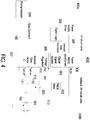
- FIG. 4 shows a gate driver circuit 400, which is one implementation of the gate driver circuit 200 of FIG. 2 .
- the circuitry of the gate driver circuit 400 is divided into a low-voltage domain 400a and a high-voltage domain 400b.
- the low-voltage domain 400a includes logic circuits that provide the control functions of the gate driver circuit 400
- the high-voltage domain 400b includes a high-voltage circuitry that drives the gate terminal 102 of the IGBT 101.
- Circuitry in the low-voltage domain 400a may be isolated from circuitry in the high-voltage domain 400b using conventional isolation techniques, such as optical isolation or other semiconductor devices.
- a power supply transformer 308 implements the higher supply voltage (e.g., 18.5 volts) of the higher-voltage power supply circuit 202 of FIG. 2 .
- the power supply transformer 308 is enabled and initialized by a low-voltage logic circuit (i.e., power supply driver 305).
- the control circuit 204 of FIG. 2 is implemented in the gate driver circuit 400 by a microprocessor 204, which issues the input control signal 106 to a logic circuit 306 and an isolated gate driver integrated circuit 307.
- the isolated gate driver integrated circuit 307 which receives the higher supply voltage from the higher-voltage power supply circuit 202, includes a voltage regulator 309 which provides a regulated output voltage (e.g., 15 volts) on the terminal 112.
- the isolated gate driver integrated circuit 307 implements the power supply circuit 109.
- the buffer stage 108 is also implemented in the isolated gate driver integrated circuit 307 by supplying the voltage at the terminal 112 to a terminal 110 during turn-on and by grounding terminal 111 during turn-off.
- the isolated gate driver integrated circuit 307 may be implemented by, for example, an MC33GD3100 integrated circuit from NXP semiconductors N.V.
- the digital logic circuit 306 delays the input control signal 106 by the predetermine delay (e.g., time interval (t 1 - t 0 ) in FIG. 3 ).
- the delayed input control signal 106 enters the high-voltage domain 400b through the digital signal isolator circuit 301 to turn on PMOS driver 302 which, in turn, turns on a PMOS transistor 303.
- Conducting the PMOS transistor 303 places the higher supply voltage of the power supply transformer 308 on the terminal 112.
- the PMOS driver 302 may be implemented by a bipolar transistor (e.g., a un2217 bipolar transistor) driving an RC circuit that achieves a more gradual slew rate (i.e., with an RC time constant) to transition to the higher supply voltage.
- the voltage regulator 309 turns off, and the higher supply voltage is provided on the terminal 110 of the turn-on resistor Ron.
- the PMOS driver 302 turns off the PMOS transistor 303 and the terminal 112 returns to the regulated output voltage of the voltage regulator 309.
- the method of the present invention drives the gate terminal of a power semiconductor device at a higher power supply voltage to achieve a reduced saturation voltage in the power semiconductor device during conduction.
- the trade-off in a conventional gate driver circuit between a lower saturation voltage when the power semiconductor device is conducting and a high short-circuit current is avoided. Since the voltage at the gate terminal of the power semiconductor device is increased during its conducting state, the power semiconductor device's conduction loss is reduced, thereby resulting in both enhanced system efficiency and a reduced thermal stress.
Abstract

Description
- The present invention relates to driver circuits for power semiconductor devices, such as driver circuits for insulated-gate bipolar transistors (IGBTs) or metal-oxide-semiconductor field-effect transistors (MOSFETs) in high-voltage, high-current applications.
-
FIG. 1 shows a conventionalgate driver circuit 100 for driving a gate terminal of apower semiconductor device 101. InFIG. 1 , thepower semiconductor device 101 is exemplified by an IGBT; however, thepower semiconductor device 101 may be any one of numerous other devices (e.g., a MOSFET). As known to those of ordinary skill in the art, the conventionalgate driver circuit 100 often includes also signal isolation, power supply, monitoring and protection circuits. These other circuits are omitted fromFIG. 1 , for clarity of illustration. As shown inFIG. 1 , thegate driver circuit 100 includes (i) abuffer stage 108 formed, for example, by bipolar junction transistors (BJTs) NPN BJT Q1 and PNP BJT Q2; and (ii) turn-on and turn-off gate resistors Ron and Roff. Thebuffer stage 108 is connected between a power supply circuit 109 (e.g., + 15 volts) and the ground reference. Thegate driver circuit 100 receives an input control signal 106 (e.g., an input control signal from a microprocessor) and provides an output signal at thegate terminal 102 of the IGBT 101. Theinput control signal 106 causes thebuffer stage 108 to turn on either the NPN BJT Q1 or the PNP BJT Q2 to charge or discharge thegate terminal 102 of theIGBT 101. Although the NPN BJT Q1 and PNP BJT Q2 are used to illustrate thebuffer stage 108, other switching devices, such as MOSFETs, may also be used to implement thebuffer stage 108. When theinput control signal 106 is at a high voltage, the NPN BJT Q1 is conducting, thereby charging the capacitance of thegate terminal 102 of theIGBT 101 to the voltage of thepower supply circuit 109 through the resistor Ron. Conversely, when theinput control signal 106 is at a low voltage, the PNP BJT Q2 is conducting, thereby discharging the capacitance at thegate terminal 102 of theIGBT 101 to ground through the resistor Roff. - Because of the transconductance of the
IGBT 101, current iC at acollector terminal 103 of theIGBT 101 is determined by the gate-emitter voltage (VGE) across thegate terminal 102 and anemitter terminal 104 of theIGBT 101. The higher voltage VGE is, the higher is current iC, which results in a lower collector-emitter voltage (VCE) at which current iC becomes saturated. To achieve the lowest possible conduction losses, a high voltage from thepower supply circuit 109 is preferred. However, the resulting higher gate-emitter voltage VGE may result in a correspondingly higher short-circuit current, if a short-circuit condition occurs. This is because, under a short circuit condition, the higher gate-emitter voltage (VGE) causes the collector current iC to increase more rapidly than when a lower gate-emitter voltage is present. Also, as thegate terminal 102 is fully charged, the collector current iC has a higher value, as the IGBT 101 is operating at a higher desaturation current level. Taking all these factors into consideration, the output voltage of thepower supply circuit 109 is usually selected, as a tradeoff, to be +15 volts. - Various schemes to improve the gate driver circuit of a power semiconductor device are known in the prior art. For example,
U.S. Patent 7,265,601 ("Ahmad "), entitled "Adaptive Gate Drive Voltage Circuit", discloses a method that reduces losses in a DC/DC converter by optimizing gate drive voltage. In Ahmad, the driver circuit adjusts the gate voltage based on the output load current; specifically, the gate voltage is reduced at a low load current and increased at a high load current. As another example,U.S. Patent 9,444,448 ("Wagoner - According to one embodiment of the present invention, a gate driver circuit receiving an input control signal and providing a voltage at a gate terminal of a semiconductor switching device (e.g., an IGBT) may include: (i) a first voltage source providing a first voltage; (ii) a second voltage source providing a second voltage, wherein the first voltage is higher than the second voltage; and (iii) a selector circuit selecting either the first voltage or the second voltage to be placed on the gate terminal of the semiconductor switching device based on the input control signal's logic state. The selector circuit may delay the input control signal by a predetermined time interval.
- In one embodiment, the selector circuit includes (i) a first transistor providing the first voltage source to the gate terminal of the semiconductor switching device in a conducting state, the first transistor having a gate terminal that receives an enable signal that causes it to switch between the conducting state and a non-conducting state; and (ii) a second transistor receiving the input control signal and providing the enable signal to the gate terminal of the first transistor according to the input control signal's logic state. An RC circuit may be provided in the signal path of the enable signal, such that, when the first transistor connects the first voltage source to the gate terminal of the semiconductor switching device, the voltage at the gate terminal of the semiconductor switching device rises to the first voltage at a slew rate determined by the RC circuit.
- In one embodiment, a buffer stage is connected between a power supply terminal and a ground reference, wherein the selector circuit provides the selected voltage at the power supply terminal of the buffer stage, and wherein the buffer stage has an output terminal coupled to the gate terminal of the semiconductor switching device, and wherein the buffer stage provides the voltage at its power supply terminal to its output terminal based on the input control signal's logic state. The output terminal of the buffer stage may be coupled to the gate terminal of the semiconductor switching device by a resistor.
- In one embodiment, the second voltage source may include a voltage regulator that receives the first voltage as an input voltage, and wherein the voltage regulator provides the second voltage as a regulated output voltage.
- In one embodiment, the circuitry in the gate driver circuit is divided into a high-voltage domain and a low-voltage domain that are isolated from each other, wherein the first and the second voltages are signals in the high-voltage domain and wherein the input control signal is a signal in the low-voltage domain.
- The input control signal may be provided from a control circuit, such as a microprocessor.
- The present invention is better understood upon consideration of the detailed description below in conjunction with the drawings.
-
-
FIG. 1 shows a conventionalgate driver circuit 100 for driving a gate terminal of apower semiconductor device 101; -
FIG. 2 shows agate driver circuit 200 in accordance with one embodiment of the present invention; -
FIG. 3 illustrates an operation of a powersupply selector circuit 203 in accordance with one embodiment of the present invention; and -
FIG. 4 shows agate driver circuit 400, which is one implementation of thegate driver circuit 200 ofFIG. 2 . - To facilitate cross-referencing among the FIG.s, like elements are assigned like reference numerals.
- The present disclosure will now be described more specifically with reference to the following embodiments. It is to be noted that the following descriptions of preferred embodiments of this disclosure are presented herein for purpose of illustration and description only. It is not intended to be exhaustive or to be limited to the precise form disclosed.
- The present invention provides a gate driver circuit that provides an adjustable output power supply voltage for driving a gate terminal of a power semiconductor device. The adjustable output power supply voltage reduces the saturation voltage in the power semiconductor device during turn-on, without compromising its desirable short-circuit current characteristics.
FIG. 2 shows agate driver circuit 200 in accordance with one embodiment of the present invention. InFIG. 2 , in addition to apower supply circuit 109,buffer stage 108, turn-on and turn-off resistors Ron and Roff ofFIG. 1 , thegate driver circuit 200 also includes a higher-voltagepower supply circuit 202, a powersupply selection circuit 201, a powersupply selector circuit 203 and acontrol circuit 204. In thegate driver circuit 200, the powersupply selector circuit 203 causes the powersupply selection circuit 201 to select the output voltage of either thepower supply circuit 109 or the higher-voltagepower supply circuit 202 to place at aterminal 112 as the power supply voltage to drive agate terminal 102 of anIGBT 101, during different times of the IGBT operations. The higher-voltagepower supply circuit 202 provides at the terminal 112 a higher voltage (e.g., 18.5 volts) than the voltage (e.g., 15 volts) supplied by thepower supply circuit 109. The powersupply selection circuit 201 may be implemented by one or more semiconductor switches and the powersupply selector circuit 203 may be implemented by a logic circuit that operates the switches in the powersupply selection circuit 201. -
FIG. 3 illustrates an operation of the powersupply selector circuit 203 in accordance with one embodiment of the present invention. As shown inFIG. 3 ,waveform 351 represents aninput control signal 106 received into thebuffer stage 108 and the powersupply selector circuit 203.Waveform 352 represents the voltage waveform at thegate terminal 102. When the IGBT 101 is turned off, the voltage at theterminal 112 is provided by the power supply circuit 109 (i.e., 15 volts). When theinput control signal 106 goes high at time t0, turn-on transistor Q1 turns on and thegate terminal 102 of theIGBT 101 goes to the lower supply voltage (i.e., 15 volts), such that collector current iC increases at a limited slew rate. Therefore, if a short-circuit condition exists at this time, the short-circuit current is limited by the lower power supply voltage. With the lower power supply voltage at itsgate terminal 102, the desaturation current in the IGBT 101 is also limited. - After a predetermined delay (i.e., time interval (t1 - t0)), the power
supply selector circuit 203 causes the voltage at theterminal 112 to be sourced from the higher-voltage power supply 202 (e.g., at 18.5 volts), which increases the voltage at thegate terminal 102 of theIGBT 101. At this higher voltage, theIGBT 101's saturation voltage across acollector terminal 103 and an emitter terminal 104 (i.e., VCE) is reduced. When theinput control signal 106 returns to low, the powersupply selector circuit 203 causes the voltage at theterminal 112 to be sourced from the power supply circuit 109 (i.e., returning the voltage at theterminal 112 to 15 volts). In some embodiments, the transition between thepower supply circuit 109 to the higher-voltage power supply circuit 202 (i.e., from 15 volts to 18.5 volts), and vice versa, can occur gradually over a predetermined time period. For example, the transition can be controlled by an RC circuit; in that case, the voltage at the terminal 112 rises or falls at a rate that may be characterized by a time constant. -
FIG. 4 shows agate driver circuit 400, which is one implementation of thegate driver circuit 200 ofFIG. 2 . As shown inFIG. 4 , the circuitry of thegate driver circuit 400 is divided into a low-voltage domain 400a and a high-voltage domain 400b. The low-voltage domain 400a includes logic circuits that provide the control functions of thegate driver circuit 400, and the high-voltage domain 400b includes a high-voltage circuitry that drives thegate terminal 102 of theIGBT 101. Circuitry in the low-voltage domain 400a may be isolated from circuitry in the high-voltage domain 400b using conventional isolation techniques, such as optical isolation or other semiconductor devices. - As show in
FIG. 4 , apower supply transformer 308 implements the higher supply voltage (e.g., 18.5 volts) of the higher-voltagepower supply circuit 202 ofFIG. 2 . Thepower supply transformer 308 is enabled and initialized by a low-voltage logic circuit (i.e., power supply driver 305). Thecontrol circuit 204 ofFIG. 2 is implemented in thegate driver circuit 400 by amicroprocessor 204, which issues theinput control signal 106 to alogic circuit 306 and an isolated gate driver integratedcircuit 307. The isolated gate driver integratedcircuit 307, which receives the higher supply voltage from the higher-voltagepower supply circuit 202, includes avoltage regulator 309 which provides a regulated output voltage (e.g., 15 volts) on theterminal 112. In this manner, the isolated gate driver integratedcircuit 307 implements thepower supply circuit 109. In addition, thebuffer stage 108 is also implemented in the isolated gate driver integratedcircuit 307 by supplying the voltage at the terminal 112 to a terminal 110 during turn-on and by grounding terminal 111 during turn-off. The isolated gate driver integratedcircuit 307 may be implemented by, for example, an MC33GD3100 integrated circuit from NXP semiconductors N.V. - In one embodiment, the
digital logic circuit 306 delays theinput control signal 106 by the predetermine delay (e.g., time interval (t1 - t0) inFIG. 3 ). The delayedinput control signal 106 enters the high-voltage domain 400b through the digitalsignal isolator circuit 301 to turn onPMOS driver 302 which, in turn, turns on aPMOS transistor 303. Conducting thePMOS transistor 303 places the higher supply voltage of thepower supply transformer 308 on theterminal 112. ThePMOS driver 302 may be implemented by a bipolar transistor (e.g., a un2217 bipolar transistor) driving an RC circuit that achieves a more gradual slew rate (i.e., with an RC time constant) to transition to the higher supply voltage. As the voltage at the terminal 112 rises, thevoltage regulator 309 turns off, and the higher supply voltage is provided on theterminal 110 of the turn-on resistor Ron. During turn-off, thePMOS driver 302 turns off thePMOS transistor 303 and the terminal 112 returns to the regulated output voltage of thevoltage regulator 309. - Without impacting short-circuit performance, the method of the present invention drives the gate terminal of a power semiconductor device at a higher power supply voltage to achieve a reduced saturation voltage in the power semiconductor device during conduction. In this manner, the trade-off in a conventional gate driver circuit between a lower saturation voltage when the power semiconductor device is conducting and a high short-circuit current is avoided. Since the voltage at the gate terminal of the power semiconductor device is increased during its conducting state, the power semiconductor device's conduction loss is reduced, thereby resulting in both enhanced system efficiency and a reduced thermal stress.
Claims (11)
- A gate driver circuit (200, 400) receiving an input control signal (106) and providing a voltage at a gate terminal (102) of a semiconductor switching device (101), comprising:a first voltage source (202) providing a first voltage;a second voltage source (109) providing a second voltage, wherein the first voltage is higher than the second voltage;a selector circuit (203) selecting either the first voltage or the second voltage to be placed on the gate terminal (102) of the semiconductor switching device (101) based on the input control signal's logic state.
- The gate driver circuit (200, 400) of Claim 1, wherein the selector circuit (203) delays the input control signal (106) by a predetermined time interval.
- The gate driver circuit (200, 400) of Claim 1, wherein the selector circuit (203) comprises:a first transistor (303) providing the first voltage source (202) to the gate terminal (102) of the semiconductor switching device (101) in a conducting state, the first transistor (303) having a gate terminal that receives an enable signal that causes it to switch between the conducting state and a non-conducting state; anda second transistor (302) receiving the input control signal (106) and providing the enable signal to the gate terminal of the first transistor (303) according to the input control signal's logic state.
- The gate driver circuit (200, 400) of Claim 3, further comprising an RC circuit in the signal path of the enable signal, such that when the first transistor (303) connects the first voltage source (202) to the gate terminal (102) of the semiconductor switching device (101), the voltage at the gate terminal (102) of the semiconductor switching device (101) rises to the first voltage at a slew rate determined by the RC circuit.
- The gate driver circuit (200, 400) of Claim 1, further comprising a buffer stage (108) connected between a power supply terminal (112) and a ground reference, wherein the selector circuit (203) provides the selected voltage at the power supply terminal (112) of the buffer stage (108).
- The gate driver circuit (200, 400) of Claim 5, wherein the buffer stage (108) has an output terminal coupled to the gate terminal (102) of the semiconductor switching device (101), and wherein the buffer stage (108) provides the voltage at its power supply terminal (112) to its output terminal based on the input control signal's logic state.
- The gate driver circuit (200, 400) of Claim 6, wherein the output terminal of the buffer stage (108) is coupled to the gate terminal (102) of the semiconductor switching device (101) by a resistor (Ron, Roff).
- The gate driver circuit (200, 400) of Claim 1, wherein the second voltage source (109) comprises a voltage regulator (309) receiving the first voltage as an input voltage, and wherein the voltage regulator (309) provides the second voltage as a regulated output voltage.
- The gate driver circuit (200, 400) of Claim 1, comprising a high-voltage domain (400b) and a low-voltage domain (400a) that are isolated from each other, wherein the first and the second voltages are signals in the high-voltage domain (400b) and wherein the input control signal (106) is a signal in the low-voltage domain (400a).
- The gate driver circuit (200, 400) of Claim 1, wherein the input control signal (106) is received from a control circuit (204).
- The gate driver circuit (200, 400) of Claim 10, wherein the control circuit (204) comprises a microprocessor (204).
Applications Claiming Priority (1)
| Application Number | Priority Date | Filing Date | Title |
|---|---|---|---|
| US16/837,896 US11165422B2 (en) | 2020-04-01 | 2020-04-01 | Gate driver circuit with reduced power semiconductor conduction loss |
Publications (1)
| Publication Number | Publication Date |
|---|---|
| EP3890190A1 true EP3890190A1 (en) | 2021-10-06 |
Family
ID=72290935
Family Applications (1)
| Application Number | Title | Priority Date | Filing Date |
|---|---|---|---|
| EP20193398.3A Pending EP3890190A1 (en) | 2020-04-01 | 2020-08-28 | Gate driver circuit with reduced power semiconductor conduction loss |
Country Status (3)
| Country | Link |
|---|---|
| US (1) | US11165422B2 (en) |
| EP (1) | EP3890190A1 (en) |
| CN (1) | CN113497610A (en) |
Families Citing this family (4)
| Publication number | Priority date | Publication date | Assignee | Title |
|---|---|---|---|---|
| IT201900011544A1 (en) | 2019-07-11 | 2021-01-11 | St Microelectronics Srl | PILOTING CIRCUIT FOR A HALF-BRIDGE |
| IT201900023787A1 (en) * | 2019-12-12 | 2021-06-12 | St Microelectronics Srl | HALF-BRIDGE CIRCUIT |
| JP2023037933A (en) * | 2021-09-06 | 2023-03-16 | 三菱電機株式会社 | Semiconductor element drive circuit and semiconductor element drive device |
| US20230111154A1 (en) * | 2021-10-08 | 2023-04-13 | Semiconductor Components Industries, Llc | Gate driver |
Citations (6)
| Publication number | Priority date | Publication date | Assignee | Title |
|---|---|---|---|---|
| US6333665B1 (en) * | 1999-02-26 | 2001-12-25 | Kabushiki Kaisha Toshiba | Gate circuit for insulated gate semiconductor device |
| US7265601B2 (en) | 2004-08-23 | 2007-09-04 | International Rectifier Corporation | Adaptive gate drive voltage circuit |
| US20090066402A1 (en) * | 2007-09-12 | 2009-03-12 | Mitsubishi Electric Corporation | Gate drive circuit |
| JP2012049946A (en) * | 2010-08-30 | 2012-03-08 | Toyota Motor Corp | Driving device driving voltage driving-type element |
| US20160226386A1 (en) * | 2015-01-30 | 2016-08-04 | Denso Corporation | Driving device for semiconductor switching element and control system for power converter |
| US9444448B2 (en) | 2013-12-10 | 2016-09-13 | General Electric Company | High performance IGBT gate drive |
Family Cites Families (50)
| Publication number | Priority date | Publication date | Assignee | Title |
|---|---|---|---|---|
| US3291999A (en) | 1961-05-15 | 1966-12-13 | Westinghouse Electric Corp | Isolated multiple output circuit |
| US3335291A (en) | 1965-03-11 | 1967-08-08 | Gen Electric | Zero voltage switching circuit using gate controlled conducting devices |
| US3631528A (en) | 1970-08-14 | 1971-12-28 | Robert S Green | Low-power consumption complementary driver and complementary bipolar buffer circuits |
| US3710062A (en) | 1971-04-06 | 1973-01-09 | Environment One Corp | Metal base cookware induction heating apparatus having improved power supply and gating control circuit using infra-red temperature sensor and improved induction heating coil arrangement |
| US3953783A (en) | 1971-04-06 | 1976-04-27 | Environment/One Corporation | Low cast chopper inverter power supply and gating circuit therefor |
| US3889195A (en) | 1973-02-12 | 1975-06-10 | Texas Instruments Inc | Interlocked plural channel switches and controllable switch devices for use therein |
| JPS57186833A (en) | 1981-05-13 | 1982-11-17 | Hitachi Ltd | Switching element |
| JPH04280475A (en) | 1991-03-08 | 1992-10-06 | Fuji Electric Co Ltd | Semiconductor switching device |
| US5504449A (en) | 1992-04-09 | 1996-04-02 | Harris Corporation | Power driver circuit |
| US5656966A (en) | 1994-03-09 | 1997-08-12 | Cooper Industries, Inc. | Turbine engine ignition exciter circuit including low voltage lockout control |
| DE19634612A1 (en) | 1996-08-27 | 1998-03-12 | Siemens Ag | Method and device for optimizing the switch-off process of a non-latching, switchable power semiconductor switch |
| JP3267189B2 (en) | 1997-05-14 | 2002-03-18 | 富士電機株式会社 | Device steady-state current balance control circuit of power converter |
| US6097582A (en) | 1999-02-12 | 2000-08-01 | Wisconsin Alumni Research Foundation | Short circuit protection of IGBTs and other power switching devices |
| JP4592040B2 (en) | 1999-11-11 | 2010-12-01 | キヤノン株式会社 | Power supply device for image forming apparatus, image forming apparatus using the same, and fixing device |
| US6400579B2 (en) | 2000-03-24 | 2002-06-04 | Slobodan Cuk | Lossless switching DC to DC converter with DC transformer |
| JP3542313B2 (en) | 2000-03-30 | 2004-07-14 | 株式会社ルネサステクノロジ | Driving method of semiconductor switching element and power supply device |
| US6304460B1 (en) | 2000-05-05 | 2001-10-16 | Slobodan Cuk | Switching DC-to-DC converter utilizing a soft switching technique |
| ES2302695T3 (en) | 2000-07-13 | 2008-08-01 | Ct-Concept Technologie Ag | PROCEDURE AND DEVICE TO REGULATE, IN FUNCTION OF THE STATE, THE TRANSITORY BEHAVIOR OF POWER SEMICONDUCTOR SWITCHES. |
| JP2005006381A (en) | 2003-06-10 | 2005-01-06 | Hitachi Ltd | Drive circuit of switching element |
| CA2565453C (en) | 2004-04-26 | 2015-06-23 | Gary Pace | Adaptive gate drive for switching devices of inverter |
| JP4118252B2 (en) | 2004-05-20 | 2008-07-16 | 三菱電機株式会社 | Power semiconductor switching device |
| JP4804142B2 (en) | 2005-12-21 | 2011-11-02 | 東洋電機製造株式会社 | High-speed gate drive circuit |
| JP4816182B2 (en) * | 2006-03-23 | 2011-11-16 | 株式会社日立製作所 | Switching element drive circuit |
| JP2009219017A (en) | 2008-03-12 | 2009-09-24 | Yazaki Corp | Load control apparatus, and method of generating input pulse therefor |
| JP5284077B2 (en) | 2008-12-26 | 2013-09-11 | 株式会社日立製作所 | Semiconductor device and power conversion device using the same |
| US8598920B2 (en) * | 2009-05-19 | 2013-12-03 | Mitsubishi Electric Corporation | Gate driving circuit |
| JP5423378B2 (en) | 2009-12-15 | 2014-02-19 | 三菱電機株式会社 | Power semiconductor device for igniter |
| JP5423377B2 (en) | 2009-12-15 | 2014-02-19 | 三菱電機株式会社 | Power semiconductor device for igniter |
| EP2555397A1 (en) * | 2010-04-01 | 2013-02-06 | Hitachi Automotive Systems, Ltd. | Power converter device |
| JP5627512B2 (en) | 2011-03-04 | 2014-11-19 | 三菱電機株式会社 | Power module |
| GB2497968A (en) | 2011-12-23 | 2013-07-03 | Amantys Ltd | Switching very large numbers of power semiconductor devices in synchronisation |
| GB201206921D0 (en) | 2012-04-20 | 2012-06-06 | Amantys Ltd | Communication protocol |
| DE102012207147B4 (en) * | 2012-04-27 | 2016-01-21 | Infineon Technologies Ag | Method for driving power semiconductor switches |
| US9345112B2 (en) | 2013-03-09 | 2016-05-17 | Chia-Teh Chen | Microcontroller-based multifunctional electronic switch and lighting apparatus having the same |
| TWI554034B (en) | 2012-10-15 | 2016-10-11 | 陳家德 | Infrared ray on/off switch with automatic dimming capacity |
| CN103973277B (en) * | 2013-02-05 | 2017-06-09 | 通用电气公司 | The short-circuit protection circuit and method of insulated gate bipolar transistor |
| EP2773032A1 (en) | 2013-03-01 | 2014-09-03 | GE Energy Power Conversion Technology Ltd | Current source converter with gate turn off semiconductor elements and a special commutation mode |
| WO2014199818A1 (en) * | 2013-06-14 | 2014-12-18 | 富士電機株式会社 | Gate-driving circuit |
| GB201311997D0 (en) | 2013-07-04 | 2013-08-21 | Amantys Ltd | Synchronising parallel power switches |
| US9503072B2 (en) | 2013-08-07 | 2016-11-22 | Mitsubishi Electric Corporation | Semiconductor switching device |
| US9742272B2 (en) | 2014-06-24 | 2017-08-22 | Fuji Electric Co., Ltd. | AC-DC converter |
| JP6528575B2 (en) | 2015-07-17 | 2019-06-12 | 富士電機株式会社 | Semiconductor switching device |
| CN108337922B (en) | 2015-10-19 | 2020-12-18 | 三菱电机株式会社 | Semiconductor device drive circuit and inverter device |
| US9564891B1 (en) | 2015-10-28 | 2017-02-07 | Crydom, Inc. | Low conducted emission solid state switch |
| JP2017118717A (en) | 2015-12-24 | 2017-06-29 | 株式会社安川電機 | Gate drive circuit, inverter circuit and motor control device |
| JP6524020B2 (en) | 2016-05-19 | 2019-06-05 | 三菱電機株式会社 | Delay time correction circuit, semiconductor device drive circuit and semiconductor device |
| DE102016211403B4 (en) | 2016-06-24 | 2018-03-29 | Vincotech Gmbh | HIGH-SET CIRCUITS AND INVERTER TOPOLOGIES WITH TANDEM DIODE CIRCUIT |
| CN106208720B (en) * | 2016-09-28 | 2019-06-11 | 杰华特微电子(杭州)有限公司 | Synchronous commutating control circuit, method and switch flyback switch circuit |
| JP2019011700A (en) | 2017-06-30 | 2019-01-24 | 富士電機株式会社 | Semiconductor device for igniting internal combustion engine |
| US10778206B2 (en) * | 2018-03-20 | 2020-09-15 | Analog Devices Global Unlimited Company | Biasing of radio frequency switches for fast switching |
-
2020
- 2020-04-01 US US16/837,896 patent/US11165422B2/en active Active
- 2020-08-28 EP EP20193398.3A patent/EP3890190A1/en active Pending
- 2020-08-31 CN CN202010899269.3A patent/CN113497610A/en active Pending
Patent Citations (6)
| Publication number | Priority date | Publication date | Assignee | Title |
|---|---|---|---|---|
| US6333665B1 (en) * | 1999-02-26 | 2001-12-25 | Kabushiki Kaisha Toshiba | Gate circuit for insulated gate semiconductor device |
| US7265601B2 (en) | 2004-08-23 | 2007-09-04 | International Rectifier Corporation | Adaptive gate drive voltage circuit |
| US20090066402A1 (en) * | 2007-09-12 | 2009-03-12 | Mitsubishi Electric Corporation | Gate drive circuit |
| JP2012049946A (en) * | 2010-08-30 | 2012-03-08 | Toyota Motor Corp | Driving device driving voltage driving-type element |
| US9444448B2 (en) | 2013-12-10 | 2016-09-13 | General Electric Company | High performance IGBT gate drive |
| US20160226386A1 (en) * | 2015-01-30 | 2016-08-04 | Denso Corporation | Driving device for semiconductor switching element and control system for power converter |
Also Published As
| Publication number | Publication date |
|---|---|
| CN113497610A (en) | 2021-10-12 |
| US20210313980A1 (en) | 2021-10-07 |
| US11165422B2 (en) | 2021-11-02 |
Similar Documents
| Publication | Publication Date | Title |
|---|---|---|
| EP3890190A1 (en) | Gate driver circuit with reduced power semiconductor conduction loss | |
| US8610485B2 (en) | Gate drive circuit | |
| US8598920B2 (en) | Gate driving circuit | |
| US8994413B2 (en) | Method for driving power semiconductor switches | |
| US20010015670A1 (en) | Semiconductor power converting apparatus | |
| WO2015183482A1 (en) | Cascode switching circuit | |
| US8461881B2 (en) | High power, high speed solid state relay | |
| EP2801153B1 (en) | Apparatus and method for control of semiconductor switching devices | |
| CN112117887A (en) | Adaptive threshold control system for detecting and adjusting duration of operating region during turn-on and turn-off of transistor | |
| CN111917403A (en) | Gate driver circuit for reducing dead time inefficiency | |
| Frank | Simple slew-rate control technique cuts switching losses | |
| US10985752B2 (en) | Hybrid drive circuit | |
| JP6706876B2 (en) | Power module | |
| EP1361652A2 (en) | Switching circuit | |
| US20240097671A1 (en) | Semiconductor device | |
| US20230053929A1 (en) | Driving apparatus | |
| WO2023162032A1 (en) | Gate drive circuit and power conversion device using same | |
| JP7052409B2 (en) | Pulse current application circuit and its control method | |
| US20230412154A1 (en) | Gate drive circuit, and semiconductor breaker | |
| US20230188134A1 (en) | Gate driver circuits with independently tunable performance characteristics | |
| TWI676355B (en) | Hybrid drive circuit | |
| JP6312946B1 (en) | Power semiconductor element drive circuit and motor drive device | |
| CN114696595A (en) | Drive device | |
| CN116683752A (en) | Drive control circuit and control method | |
| KR20230103987A (en) | Current Changeable MOSFET Gate Drive Circuit |
Legal Events
| Date | Code | Title | Description |
|---|---|---|---|
| PUAI | Public reference made under article 153(3) epc to a published international application that has entered the european phase |
Free format text: ORIGINAL CODE: 0009012 |
|
| STAA | Information on the status of an ep patent application or granted ep patent |
Free format text: STATUS: THE APPLICATION HAS BEEN PUBLISHED |
|
| AK | Designated contracting states |
Kind code of ref document: A1 Designated state(s): AL AT BE BG CH CY CZ DE DK EE ES FI FR GB GR HR HU IE IS IT LI LT LU LV MC MK MT NL NO PL PT RO RS SE SI SK SM TR |
|
| STAA | Information on the status of an ep patent application or granted ep patent |
Free format text: STATUS: REQUEST FOR EXAMINATION WAS MADE |
|
| 17P | Request for examination filed |
Effective date: 20220321 |
|
| RBV | Designated contracting states (corrected) |
Designated state(s): AL AT BE BG CH CY CZ DE DK EE ES FI FR GB GR HR HU IE IS IT LI LT LU LV MC MK MT NL NO PL PT RO RS SE SI SK SM TR |
|
| STAA | Information on the status of an ep patent application or granted ep patent |
Free format text: STATUS: EXAMINATION IS IN PROGRESS |
|
| 17Q | First examination report despatched |
Effective date: 20230825 |