EP3890008A1 - Semiconductor module assembly comprising a joint layer with an elastic grid between a semiconductor die and a substrate and manufacturing process of such assembly - Google Patents
Semiconductor module assembly comprising a joint layer with an elastic grid between a semiconductor die and a substrate and manufacturing process of such assembly Download PDFInfo
- Publication number
- EP3890008A1 EP3890008A1 EP20315090.9A EP20315090A EP3890008A1 EP 3890008 A1 EP3890008 A1 EP 3890008A1 EP 20315090 A EP20315090 A EP 20315090A EP 3890008 A1 EP3890008 A1 EP 3890008A1
- Authority
- EP
- European Patent Office
- Prior art keywords
- grid
- die
- substrate
- cells
- paste
- Prior art date
- Legal status (The legal status is an assumption and is not a legal conclusion. Google has not performed a legal analysis and makes no representation as to the accuracy of the status listed.)
- Withdrawn
Links
Images



Classifications
-
- H—ELECTRICITY
- H10—SEMICONDUCTOR DEVICES; ELECTRIC SOLID-STATE DEVICES NOT OTHERWISE PROVIDED FOR
- H10W—GENERIC PACKAGES, INTERCONNECTIONS, CONNECTORS OR OTHER CONSTRUCTIONAL DETAILS OF DEVICES COVERED BY CLASS H10
- H10W72/00—Interconnections or connectors in packages
- H10W72/071—Connecting or disconnecting
- H10W72/073—Connecting or disconnecting of die-attach connectors
-
- H—ELECTRICITY
- H10—SEMICONDUCTOR DEVICES; ELECTRIC SOLID-STATE DEVICES NOT OTHERWISE PROVIDED FOR
- H10W—GENERIC PACKAGES, INTERCONNECTIONS, CONNECTORS OR OTHER CONSTRUCTIONAL DETAILS OF DEVICES COVERED BY CLASS H10
- H10W72/00—Interconnections or connectors in packages
- H10W72/01—Manufacture or treatment
- H10W72/013—Manufacture or treatment of die-attach connectors
-
- H—ELECTRICITY
- H10—SEMICONDUCTOR DEVICES; ELECTRIC SOLID-STATE DEVICES NOT OTHERWISE PROVIDED FOR
- H10W—GENERIC PACKAGES, INTERCONNECTIONS, CONNECTORS OR OTHER CONSTRUCTIONAL DETAILS OF DEVICES COVERED BY CLASS H10
- H10W72/00—Interconnections or connectors in packages
- H10W72/01—Manufacture or treatment
- H10W72/013—Manufacture or treatment of die-attach connectors
- H10W72/01321—Manufacture or treatment of die-attach connectors using local deposition
- H10W72/01323—Manufacture or treatment of die-attach connectors using local deposition in liquid form, e.g. by dispensing droplets or by screen printing
-
- H—ELECTRICITY
- H10—SEMICONDUCTOR DEVICES; ELECTRIC SOLID-STATE DEVICES NOT OTHERWISE PROVIDED FOR
- H10W—GENERIC PACKAGES, INTERCONNECTIONS, CONNECTORS OR OTHER CONSTRUCTIONAL DETAILS OF DEVICES COVERED BY CLASS H10
- H10W72/00—Interconnections or connectors in packages
- H10W72/01—Manufacture or treatment
- H10W72/013—Manufacture or treatment of die-attach connectors
- H10W72/01321—Manufacture or treatment of die-attach connectors using local deposition
- H10W72/01325—Manufacture or treatment of die-attach connectors using local deposition in solid form
-
- H—ELECTRICITY
- H10—SEMICONDUCTOR DEVICES; ELECTRIC SOLID-STATE DEVICES NOT OTHERWISE PROVIDED FOR
- H10W—GENERIC PACKAGES, INTERCONNECTIONS, CONNECTORS OR OTHER CONSTRUCTIONAL DETAILS OF DEVICES COVERED BY CLASS H10
- H10W72/00—Interconnections or connectors in packages
- H10W72/071—Connecting or disconnecting
- H10W72/073—Connecting or disconnecting of die-attach connectors
- H10W72/07321—Aligning
- H10W72/07323—Active alignment, e.g. using optical alignment using marks or sensors
-
- H—ELECTRICITY
- H10—SEMICONDUCTOR DEVICES; ELECTRIC SOLID-STATE DEVICES NOT OTHERWISE PROVIDED FOR
- H10W—GENERIC PACKAGES, INTERCONNECTIONS, CONNECTORS OR OTHER CONSTRUCTIONAL DETAILS OF DEVICES COVERED BY CLASS H10
- H10W72/00—Interconnections or connectors in packages
- H10W72/071—Connecting or disconnecting
- H10W72/073—Connecting or disconnecting of die-attach connectors
- H10W72/07331—Connecting techniques
-
- H—ELECTRICITY
- H10—SEMICONDUCTOR DEVICES; ELECTRIC SOLID-STATE DEVICES NOT OTHERWISE PROVIDED FOR
- H10W—GENERIC PACKAGES, INTERCONNECTIONS, CONNECTORS OR OTHER CONSTRUCTIONAL DETAILS OF DEVICES COVERED BY CLASS H10
- H10W72/00—Interconnections or connectors in packages
- H10W72/071—Connecting or disconnecting
- H10W72/073—Connecting or disconnecting of die-attach connectors
- H10W72/07331—Connecting techniques
- H10W72/07336—Soldering or alloying
-
- H—ELECTRICITY
- H10—SEMICONDUCTOR DEVICES; ELECTRIC SOLID-STATE DEVICES NOT OTHERWISE PROVIDED FOR
- H10W—GENERIC PACKAGES, INTERCONNECTIONS, CONNECTORS OR OTHER CONSTRUCTIONAL DETAILS OF DEVICES COVERED BY CLASS H10
- H10W72/00—Interconnections or connectors in packages
- H10W72/071—Connecting or disconnecting
- H10W72/073—Connecting or disconnecting of die-attach connectors
- H10W72/07351—Connecting or disconnecting of die-attach connectors characterised by changes in properties of the die-attach connectors during connecting
- H10W72/07352—Connecting or disconnecting of die-attach connectors characterised by changes in properties of the die-attach connectors during connecting changes in structures or sizes
-
- H—ELECTRICITY
- H10—SEMICONDUCTOR DEVICES; ELECTRIC SOLID-STATE DEVICES NOT OTHERWISE PROVIDED FOR
- H10W—GENERIC PACKAGES, INTERCONNECTIONS, CONNECTORS OR OTHER CONSTRUCTIONAL DETAILS OF DEVICES COVERED BY CLASS H10
- H10W72/00—Interconnections or connectors in packages
- H10W72/30—Die-attach connectors
- H10W72/321—Structures or relative sizes of die-attach connectors
-
- H—ELECTRICITY
- H10—SEMICONDUCTOR DEVICES; ELECTRIC SOLID-STATE DEVICES NOT OTHERWISE PROVIDED FOR
- H10W—GENERIC PACKAGES, INTERCONNECTIONS, CONNECTORS OR OTHER CONSTRUCTIONAL DETAILS OF DEVICES COVERED BY CLASS H10
- H10W72/00—Interconnections or connectors in packages
- H10W72/30—Die-attach connectors
- H10W72/321—Structures or relative sizes of die-attach connectors
- H10W72/325—Die-attach connectors having a filler embedded in a matrix
-
- H—ELECTRICITY
- H10—SEMICONDUCTOR DEVICES; ELECTRIC SOLID-STATE DEVICES NOT OTHERWISE PROVIDED FOR
- H10W—GENERIC PACKAGES, INTERCONNECTIONS, CONNECTORS OR OTHER CONSTRUCTIONAL DETAILS OF DEVICES COVERED BY CLASS H10
- H10W72/00—Interconnections or connectors in packages
- H10W72/30—Die-attach connectors
- H10W72/331—Shapes of die-attach connectors
-
- H—ELECTRICITY
- H10—SEMICONDUCTOR DEVICES; ELECTRIC SOLID-STATE DEVICES NOT OTHERWISE PROVIDED FOR
- H10W—GENERIC PACKAGES, INTERCONNECTIONS, CONNECTORS OR OTHER CONSTRUCTIONAL DETAILS OF DEVICES COVERED BY CLASS H10
- H10W72/00—Interconnections or connectors in packages
- H10W72/30—Die-attach connectors
- H10W72/351—Materials of die-attach connectors
- H10W72/352—Materials of die-attach connectors comprising metals or metalloids, e.g. solders
-
- H—ELECTRICITY
- H10—SEMICONDUCTOR DEVICES; ELECTRIC SOLID-STATE DEVICES NOT OTHERWISE PROVIDED FOR
- H10W—GENERIC PACKAGES, INTERCONNECTIONS, CONNECTORS OR OTHER CONSTRUCTIONAL DETAILS OF DEVICES COVERED BY CLASS H10
- H10W72/00—Interconnections or connectors in packages
- H10W72/30—Die-attach connectors
- H10W72/351—Materials of die-attach connectors
- H10W72/353—Materials of die-attach connectors not comprising solid metals or solid metalloids, e.g. ceramics
-
- H—ELECTRICITY
- H10—SEMICONDUCTOR DEVICES; ELECTRIC SOLID-STATE DEVICES NOT OTHERWISE PROVIDED FOR
- H10W—GENERIC PACKAGES, INTERCONNECTIONS, CONNECTORS OR OTHER CONSTRUCTIONAL DETAILS OF DEVICES COVERED BY CLASS H10
- H10W72/00—Interconnections or connectors in packages
- H10W72/30—Die-attach connectors
- H10W72/351—Materials of die-attach connectors
- H10W72/353—Materials of die-attach connectors not comprising solid metals or solid metalloids, e.g. ceramics
- H10W72/354—Materials of die-attach connectors not comprising solid metals or solid metalloids, e.g. ceramics comprising polymers
-
- H—ELECTRICITY
- H10—SEMICONDUCTOR DEVICES; ELECTRIC SOLID-STATE DEVICES NOT OTHERWISE PROVIDED FOR
- H10W—GENERIC PACKAGES, INTERCONNECTIONS, CONNECTORS OR OTHER CONSTRUCTIONAL DETAILS OF DEVICES COVERED BY CLASS H10
- H10W72/00—Interconnections or connectors in packages
- H10W72/851—Dispositions of multiple connectors or interconnections
- H10W72/874—On different surfaces
- H10W72/884—Die-attach connectors and bond wires
-
- H—ELECTRICITY
- H10—SEMICONDUCTOR DEVICES; ELECTRIC SOLID-STATE DEVICES NOT OTHERWISE PROVIDED FOR
- H10W—GENERIC PACKAGES, INTERCONNECTIONS, CONNECTORS OR OTHER CONSTRUCTIONAL DETAILS OF DEVICES COVERED BY CLASS H10
- H10W72/00—Interconnections or connectors in packages
- H10W72/90—Bond pads, in general
- H10W72/931—Shapes of bond pads
-
- H—ELECTRICITY
- H10—SEMICONDUCTOR DEVICES; ELECTRIC SOLID-STATE DEVICES NOT OTHERWISE PROVIDED FOR
- H10W—GENERIC PACKAGES, INTERCONNECTIONS, CONNECTORS OR OTHER CONSTRUCTIONAL DETAILS OF DEVICES COVERED BY CLASS H10
- H10W74/00—Encapsulations, e.g. protective coatings
-
- H—ELECTRICITY
- H10—SEMICONDUCTOR DEVICES; ELECTRIC SOLID-STATE DEVICES NOT OTHERWISE PROVIDED FOR
- H10W—GENERIC PACKAGES, INTERCONNECTIONS, CONNECTORS OR OTHER CONSTRUCTIONAL DETAILS OF DEVICES COVERED BY CLASS H10
- H10W90/00—Package configurations
- H10W90/701—Package configurations characterised by the relative positions of pads or connectors relative to package parts
- H10W90/731—Package configurations characterised by the relative positions of pads or connectors relative to package parts of die-attach connectors
- H10W90/734—Package configurations characterised by the relative positions of pads or connectors relative to package parts of die-attach connectors between a chip and a stacked insulating package substrate, interposer or RDL
-
- H—ELECTRICITY
- H10—SEMICONDUCTOR DEVICES; ELECTRIC SOLID-STATE DEVICES NOT OTHERWISE PROVIDED FOR
- H10W—GENERIC PACKAGES, INTERCONNECTIONS, CONNECTORS OR OTHER CONSTRUCTIONAL DETAILS OF DEVICES COVERED BY CLASS H10
- H10W90/00—Package configurations
- H10W90/701—Package configurations characterised by the relative positions of pads or connectors relative to package parts
- H10W90/751—Package configurations characterised by the relative positions of pads or connectors relative to package parts of bond wires
- H10W90/754—Package configurations characterised by the relative positions of pads or connectors relative to package parts of bond wires between a chip and a stacked insulating package substrate, interposer or RDL
Definitions
- the present disclosure concerns a semiconductor module assembly comprising an improved joint layer between a semiconductor die and a substrate and a manufacturing process for such a semiconductor module assembly.
- Power semiconductor modules usually comprise one or more power semiconductor module assemblies comprising a die or dies attached to a substrate or substrates with a joint layer.
- the power semiconductor dies need to be connected to external circuits by the both faces.
- Current die attach techniques with such interconnections are based on soldering and/or sintering.
- a classical soldering/sintering process is used to connect the die/die to a lead frame or DBC (Direct Bonded Copper) substrate. This connection is commonly called a die attach.
- DBC Direct Bonded Copper
- This connection is commonly called a die attach.
- a paste including metal particles is deposed on the substrate, heated until melting or sintering and solidified during cooling down.
- the other face of the die is normally connected through wire bonding or direct copper connections.
- the power die is attached mechanically to a substrate that usually contains a metallic layer.
- This connection called die attach, formed by a joint layer, ensures the electrical connection of a drain pad in a case of a Mosfet, a collector pad in a case of an IGBT, a cathode pad in a case of a diode to the external pinout of the power module. Furthermore, the heat created by the semiconductor is dissipated through this connection.
- This connection is formed with a joint using a paste that contains powder of metals and additives.
- the paste is deposed on the substrate layer, with a thickness inferior to 200 ⁇ m, then the die is positioned on the paste layer and temperature and some pressure is applied to the structure in order to melt or sinter the paste and finally the paste is cooled and solidifies to form the joint layer.
- the paste has a melting point higher than the temperature of operation of the power semiconductor so that the joint does remains solid during operation of the semiconductor.
- One of the main causes of power module failure is the deterioration of the joint layer.
- the joint layer ensures an electrical and thermal connection of the die to the external environment. Then, this interface is placed between two materials with different coefficient of thermal expansion (CTE), one being a semiconductor, e.g. Si (with a linear CTE of 2.56e-6/K) and other being a metal, e.g. Cu (with a linear CTE of 17e-6/K).
- CTE coefficient of thermal expansion
- the temperature swings create thermal/mechanical stress on the structure made of the die, the joint layer and the substrate that lead to formation and propagation of cracks in the joint layer that limits the lifetime of the power module.
- the present invention aims to limit propagation of cracks in the joint layer an therefore proposes a power module assembly comprising a power die attached to a substrate through a joint layer comprising solid pads of metal alloy material connecting electrically and thermally said power die to said substrate, wherein said pads are located within cells of a grid made of an elastic material and having cell walls extending between the surface of the substrate and the surface of the die facing each other.
- a grid prevents crack propagation within the joint layer while providing little thermal resistance.
- the grid may be a honeycomb shaped or square shaped lattice.
- the cells of the grid may be shaped through laser cutting.
- the elastic grid may be in formed as a tape with adhesive on both sides and be glued on both the substrate and the die;
- the elastic grid may be placed and attached on the substrate with a screen printing technique using an ink charged with high thermal conductive particles.
- the assembly of the present disclosure may be used to manufacture a power module in which the die is connected mechanically and electrically to the substrate.
- the present disclosure concerns a power module assembly which comprises a power semiconductor die or chip, a substrate such as a stack of ceramic and copper on which the die or dies are to be mechanically attached and electrically and thermally connected and a joint layer comprising paste, which is solidified through a heating and cooling process to attach said die to said stack.
- Such power modules assemblies can be used in power modules such as IGBT modules e.g. IGBT Modules S1 series of the company Mitsubishi Electric
- FIG. 1 A schematic example of prior art power module assembly with attachment of a die 5 to a substrate through a prior art joint layer 40 is given in figure 1 .
- Such attachment may be the object of cracks while ageing, as represented in figures 1 and 2 .
- Figure 1 provides a side view of a prior art assembly of a die 5 on a substrate 1 such as a copper layer which is itself attached to a base plate 11 e.g. a ceramic electrically insulating layer to form a stack as said here above.
- the die 5 is attached to the substrate 1 through the joint layer 40 where after time several cracks 45 start from a side of the joint layer.
- FIG 2 viewed from above a crack 45 initiated at a corner 43 of the joint layer propagates itself in a direction 42 along a diagonal and as time goes on has its length increasing above millimeters.
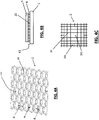
- the present disclosure proposes to incorporate a grid such as represented in figure 4A and made with an elastic material.
- the grid is in the form of a lattice having cells open in a direction perpendicular to the faces to be joined of the substrate and die.
- step D of figure 3 paste 9 is deposited in the cells of the grid 2, between the walls 20 of such grid in order to fill such cells and attach the die 5 to the substrate 1 after solidification of the paste.
- Figure 4B shows the joint layer 41 with solidified paste pads 4 and cell walls 20 of a grid in lateral cut view.
- the paste is usually an Ag paste or Cu paste or Sn based paste as known in the field of the invention and is a paste having particles of metal alloys and additives. When it is heated at a certain temperature, the paste becomes solid paste.
- the grid placed in the joint layer limits the propagation of cracks in the joint layer by confining the cracks in the interior of the grid cells with the grid walls acting as an elastic barrier that stops the cracks.
- the die 5 is assembled with the substrate through the joint layer 41 made from paste 9 in the cells of the grid 2 and the assembly is heated either to melt the metal particles of the paste in a reflow process or to sinter the particle so that such paste solidifies to provide solid pads embedded in the grid cells when the assembly is cooled.
- the die side remote from the substrate can be processed as in traditional power semiconductors manufacturing.
- the grid pattern may be a hexagonal pavement shape.
- an effective prevention of propagation of cracks starting from any point of the cell is obtained.
- Small grid wall width are achievable compared to other geometries, enabling limited reduction of thermal and electrical impedance of the joint layer, therefore limiting the increase of junction temperature of the semiconductor die, and extending its lifetime.
- a grid with a square pavement shape could also be used as described hereunder.
- the grid 2 is formed as a lattice having hexagonal cells 200 separated by walls 20 and typically the cells maximum width is typically at least ten times bigger than the width of the walls separating the cells.
- the width D of the grid cells 200 is defined as being at least 10 times larger than the width d of the grid walls, and the wall grid width is larger or equal than half the height H of the walls of the grid.
- Typical dimensions are about 500 ⁇ m to 1000 ⁇ m for the cell width D, 50 ⁇ m to 70 ⁇ m for the wall width d and 10 ⁇ m to 80 ⁇ m for the wall height H.
- the thermal resistance of the joint layer is increased by the presence of the grid in the joint layer at worse by less than 10%. This is small compared with the degradation of the thermal resistance during the lifetime of conventional power modules which is typically 30%.
- peripheral grid cells 201 of a grid 2' may be smaller than 500 ⁇ m on the borders of the joint layer, e.g. on a few rows since cracks often start from the borders or the corners of the joint layer. Reducing the width of the cells at these positions is of interest to further limit propagation of crack especially with respect to horizontal cracks that often starts from the corners.
- d 70 ⁇ m
- H 25 ⁇ m
- the cracks cannot grow from the sides or corners more than the width of the reduced width cells while inner cells may be larger to reduce the degradation of the overall thermal resistance.
- the area potentially affected by cracks is limited to a marginal portion of the die/substrate attach surface and the power module has better reliability and longer lifetime.
- the temperature of the die being smaller on the periphery of the die, the increase of the thermal resistance in this region helps to equalize the temperature over the die surface.
- the grid material is chosen to provide the capability to contract with an increase of temperature. First this helps applying a high pressure on the paste during the heating process phase and second this allows the solid paste to expand in the hot areas without extra constraint during the operation of the power semiconductor die. Contracting of the elastic grid leaves room to the rest of the joint layer to expand under high temperature, relaxing the stress during the lifetime operation of the power modules. In consequence, cracks are less prone to nucleation and to propagation and the lifetime of the power module is improved.
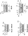
- FIGS 5A showing a segment with a length d1 where the assembly of the die 51, the joint layer 40a and the substrate 21 is at ambient temperature and figure 5B where such assembly is heated due to the losses created by the electrical power load applied to the power chip.
- FIG. 6A An example of a segment of a length close to d1 with two cells of the present grid design is given in figures 6A at ambient temperature and figure 6B under load.
- one grid wall 20 is shown with two cells filled with solidified paste pads 4, 4' between the die segment 52 and the substrate segment 22.
- the dilatation of the solidified paste pads 4 and 4' in 4a and 4'a is half the dilatation of the prior art layer 40 and in addition, the upper part 2a of the wall 2 contracts which reduces stress on the solidified paste pads 4, 4' in the cells. As this is repeated on the total length and width of the die, the total stress at the contour of the die is reduced according to the number of cells involved highly reducing the stress at the contour and corners of the die.
- the elastic grid may be shaped to desired grid shape using laser cut or screen printing and a preferred material for the grid is polyimide or the reference Elpemer® 2467 or another polymer material that can withstand the reflow temperature of the paste and which has contracting capabilities.
- the grid preferably has a 10-80 ⁇ m height that is a typical height of joint layers.
- the grid can also be colored to help its identification and placement during the manufacturing process.
- the tape shaped grid offers uniform height, helping to unify the height of the joint layer.
- the walls width may be bigger than half the thickness of the joint layer. This helps building the grid from a tape using laser cutting techniques of polyimide tapes or from an ink using a screen printing technics or the combination of the two processes and provides walls of a sufficient surface for effective adhesion to the substrate.
- FIG. 3 The process of manufacturing a power module assembly with a die connected mechanically and electrically to the substrate in accordance with the disclosure is shown in figure 3 .
- Such process starts from a substrate 1 with a receiving surface 1a for a joint layer and a die shown at A and comprises:
- the stencil may be shaped as to lie around the dimensions of the contour of the die or shaped to lie under the border of the contour dimensions of the die.
- the cooled and solid power module assembly is processed further to make a power module as in former modules.
- Application of the paste at step D can be done with a screen printing technique.
- the die and substrate are kept parallel to provide a homogeneous layer of paste 9 inside the cells of the grid without voids during the heating and cooling phases and to ensure that the thickness of the final joint layer is the same all along the die surface.
- the grid may be formed from a tape where the cells holes are made with a laser cutting process.
- the tape is the cut to form a pad of the size of the die in order to be attached to the substrate.
- An Automatic labeler may place and attach the grid on the substrate.
- the elastic grid may be formed, placed and attached on the substrate with a screen printing technique where ink is charged with high thermal conductive particles. Thus, the thermal resistance of the grid is reduced given the metallic particles.
- the elastic grid may be provided with adhesive on one or its two sides to be glued to the substrate or to the substrate and die. This helps the grid not to move during the above described manufacturing process.
- the grid could be provided in the form of a tape with adhesive on its two faces.
- the resulting assembly is used to manufacture a power component as an IGBT or other component according to the type of die used as for example shown in figure 7 where the component receiving the assembly made of the die 5, the joint layer 41 made in accordance with the present disclosure and the substrate composed by a stack of copper 1 and an electrically insulating but heat conductive layer 11 such as a ceramic layer, a heat conductive base plate 12, a housing 13, an encapsulating gel 15 and where the substrate comprises conductive lines for receiving wire bonds 14 for connecting tracks from the upper side of the die to contact elements 16, 17 that exit the power module.
- the invention of the present disclosure is not limited to the example shown and in particular, more than one die may be received in a power module.
Landscapes
- Cooling Or The Like Of Semiconductors Or Solid State Devices (AREA)
Abstract
Description
- The present disclosure concerns a semiconductor module assembly comprising an improved joint layer between a semiconductor die and a substrate and a manufacturing process for such a semiconductor module assembly.
- Power semiconductor modules usually comprise one or more power semiconductor module assemblies comprising a die or dies attached to a substrate or substrates with a joint layer.
- The power semiconductor dies need to be connected to external circuits by the both faces. Current die attach techniques with such interconnections are based on soldering and/or sintering. On one face, a classical soldering/sintering process is used to connect the die/die to a lead frame or DBC (Direct Bonded Copper) substrate. This connection is commonly called a die attach. In this process, a paste including metal particles is deposed on the substrate, heated until melting or sintering and solidified during cooling down. The other face of the die is normally connected through wire bonding or direct copper connections.
- In such modules, lifetime is mostly controlled by the package interconnections.
- Increase of the reliability of these interconnections is given by improvements in the composition of the paste, a better control of the process of the paste deposition during the assembling process and adapted package design to reduce thermal/mechanical stress and deformations taking into account the environmental stresses.
- In a classical power module, the power die is attached mechanically to a substrate that usually contains a metallic layer. This connection, called die attach, formed by a joint layer, ensures the electrical connection of a drain pad in a case of a Mosfet, a collector pad in a case of an IGBT, a cathode pad in a case of a diode to the external pinout of the power module. Furthermore, the heat created by the semiconductor is dissipated through this connection. This connection is formed with a joint using a paste that contains powder of metals and additives. In the process of assembling the module, the paste is deposed on the substrate layer, with a thickness inferior to 200µm, then the die is positioned on the paste layer and temperature and some pressure is applied to the structure in order to melt or sinter the paste and finally the paste is cooled and solidifies to form the joint layer. As known in the art, the paste has a melting point higher than the temperature of operation of the power semiconductor so that the joint does remains solid during operation of the semiconductor.
- One of the main causes of power module failure is the deterioration of the joint layer. During the lifetime of the power modules, the joint layer ensures an electrical and thermal connection of the die to the external environment. Then, this interface is placed between two materials with different coefficient of thermal expansion (CTE), one being a semiconductor, e.g. Si (with a linear CTE of 2.56e-6/K) and other being a metal, e.g. Cu (with a linear CTE of 17e-6/K).
- During operation of power modules, the temperature swings induces different expansion on the materials causing thermal/mechanical stress and consequently a fatigue mechanism takes place. Given this stress, cracks occur in the joint layer. The cracks grow with time creating voids on the layer. Furthermore, a local fragility is created when two voids are close to one another and facilitates crack propagation between these voids. One of the consequences of this deterioration is the increase of the thermal/electrical resistance of the joint, which consequently increases the temperature and accelerate even more the degradation process.
- To summarize, the temperature swings create thermal/mechanical stress on the structure made of the die, the joint layer and the substrate that lead to formation and propagation of cracks in the joint layer that limits the lifetime of the power module.
- In view of the above problem and in view of the requirements on power conversion systems which include long lifetime and high resistance to degradation, the present invention aims to limit propagation of cracks in the joint layer an therefore proposes a power module assembly comprising a power die attached to a substrate through a joint layer comprising solid pads of metal alloy material connecting electrically and thermally said power die to said substrate, wherein said pads are located within cells of a grid made of an elastic material and having cell walls extending between the surface of the substrate and the surface of the die facing each other. Such a grid prevents crack propagation within the joint layer while providing little thermal resistance.
- In preferred embodiments, the grid may be a honeycomb shaped or square shaped lattice.
- In embodiments which may be combined or alternate:
- The grid cell size may be at least ten times bigger than a grid wall width. This is a good compromise between the thermal resistance and the crack propagation;
- The width of walls of the grid cells may be larger than half of the thickness of the joint layer. This ensures a good strength of the grid;
- A maximum width of the cells of the grid may be below micrometers and preferably below 600 micrometers. This also limits propagation of cracks while limiting thermal resistance;
- The grid may have a thickness between 20 micrometers and 100 micrometers. This is in correspondence with usual joint layers height which permits to remain in the usual components dimensions while limiting the thermal resistance;
- The grid material may be such that the walls of the grid contract with an increase of temperature. This permits expansion of the joint layer material;
- The grid may be a polyimide grid. Such material provides easy handling and retracts when temperature increases;
- The grid may be made out of a single or double faced adhesive polyimide tape which simplifies the process by keeping the grid still;
- The grid may comprise peripheral cells of a reduced width with respect to central cells of the grid. Such an arrangement improves crack stoppage in the periphery of the joint layer where such cracks have a higher probability to occur;
- The present disclosure also concerns a process for manufacturing a power module assembly as disclosed above comprising:
- providing an elastic grid having a length and a width corresponding to the length and width of the semiconductor die to attach;
- placing and attaching said elastic grid on the substrate;
- placing a stencil (3) forming a frame with a shape adapted to a contour of the semiconductor die on the substrate around the grid and applying paste with a screen printing technique in the area defined by the stencil;
- removing the stencil;
- placing the power semiconductor die on top of the paste;
- applying pressure on the die to compress the assembly made of the die, the grid and paste and the substrate;
- heating the assembly up to the melting point of the paste;
- cooling the assembly to provide solid pads embedded in said grid.
- In embodiments of the process which may be alternate or combined:
The cells of the grid may be shaped through laser cutting. - The elastic grid may be in formed as a tape with adhesive on both sides and be glued on both the substrate and the die;
The elastic grid may be placed and attached on the substrate with a screen printing technique using an ink charged with high thermal conductive particles. The assembly of the present disclosure may be used to manufacture a power module in which the die is connected mechanically and electrically to the substrate. - A detailed description of exemplary embodiments of the invention will be discussed hereunder in reference to the attached drawings where:
-
Figure 1 represents a prior art joint with cracks between a substrate and a die viewed from a side; -
Figure 2 represents a prior art joint with crack viewed from above; -
Figure 3 represents manufacturing steps of a device of the present disclosure in perspective view; -
Figure 4A and 4B represent respectively a perspective view of an example of a first embodiment of a grid of the present disclosure and a schematic side cut view of a device with a grid such as infigure 4A ; -
Figure 4C represents another embodiment of a grid with square cells of different size; -
Figures 5A and 5B represent schematic side cut views of a prior art joint respectively under low and high temperature; -
Figures 6A and 6B represent schematic side cut views of the joint of the present disclosure respectively under low and high temperature; -
Figure 7 represents a power module using a device of the present disclosure. - The present disclosure concerns a power module assembly which comprises a power semiconductor die or chip, a substrate such as a stack of ceramic and copper on which the die or dies are to be mechanically attached and electrically and thermally connected and a joint layer comprising paste, which is solidified through a heating and cooling process to attach said die to said stack.
- Such power modules assemblies can be used in power modules such as IGBT modules e.g. IGBT Modules S1 series of the company Mitsubishi Electric
- A schematic example of prior art power module assembly with attachment of a
die 5 to a substrate through a prior artjoint layer 40 is given infigure 1 . Such attachment may be the object of cracks while ageing, as represented infigures 1 and 2 . -
Figure 1 provides a side view of a prior art assembly of adie 5 on asubstrate 1 such as a copper layer which is itself attached to abase plate 11 e.g. a ceramic electrically insulating layer to form a stack as said here above. Thedie 5 is attached to thesubstrate 1 through thejoint layer 40 where after timeseveral cracks 45 start from a side of the joint layer. Infigure 2 viewed from above acrack 45 initiated at acorner 43 of the joint layer propagates itself in adirection 42 along a diagonal and as time goes on has its length increasing above millimeters. - In order to limit expansion of such cracks the present disclosure proposes to incorporate a grid such as represented in
figure 4A and made with an elastic material. The grid is in the form of a lattice having cells open in a direction perpendicular to the faces to be joined of the substrate and die. - In step D of
figure 3 paste 9 is deposited in the cells of thegrid 2, between thewalls 20 of such grid in order to fill such cells and attach thedie 5 to thesubstrate 1 after solidification of the paste.Figure 4B shows thejoint layer 41 with solidifiedpaste pads 4 andcell walls 20 of a grid in lateral cut view. - The paste is usually an Ag paste or Cu paste or Sn based paste as known in the field of the invention and is a paste having particles of metal alloys and additives. When it is heated at a certain temperature, the paste becomes solid paste.
- The grid placed in the joint layer limits the propagation of cracks in the joint layer by confining the cracks in the interior of the grid cells with the grid walls acting as an elastic barrier that stops the cracks.
- As described hereunder, the
die 5 is assembled with the substrate through thejoint layer 41 made frompaste 9 in the cells of thegrid 2 and the assembly is heated either to melt the metal particles of the paste in a reflow process or to sinter the particle so that such paste solidifies to provide solid pads embedded in the grid cells when the assembly is cooled. - Once such structure is assembled, the die side remote from the substrate can be processed as in traditional power semiconductors manufacturing.
- In the embodiment of
figure 4A , the grid pattern may be a hexagonal pavement shape. Thus, an effective prevention of propagation of cracks starting from any point of the cell is obtained. Small grid wall width are achievable compared to other geometries, enabling limited reduction of thermal and electrical impedance of the joint layer, therefore limiting the increase of junction temperature of the semiconductor die, and extending its lifetime. A grid with a square pavement shape could also be used as described hereunder. - In
figure 4A thegrid 2 is formed as a lattice having hexagonal cells 200 separated bywalls 20 and typically the cells maximum width is typically at least ten times bigger than the width of the walls separating the cells. - In a preferred embodiment, the width D of the grid cells 200 is defined as being at least 10 times larger than the width d of the grid walls, and the wall grid width is larger or equal than half the height H of the walls of the grid. Typical dimensions are about 500 µm to 1000 µm for the cell width D, 50 µm to 70 µm for the wall width d and 10 µm to 80 µm for the wall height H. In a specific embodiment D=700 µm, d=70 µm and H=25 µm with a tolerance of 20%.
- Thus, the thermal resistance of the joint layer is increased by the presence of the grid in the joint layer at worse by less than 10%. This is small compared with the degradation of the thermal resistance during the lifetime of conventional power modules which is typically 30%.
- In a specific embodiment as in
figure 4C ,peripheral grid cells 201 of a grid 2' may be smaller than 500 µm on the borders of the joint layer, e.g. on a few rows since cracks often start from the borders or the corners of the joint layer. Reducing the width of the cells at these positions is of interest to further limit propagation of crack especially with respect to horizontal cracks that often starts from the corners. In example, d=70µm, H= 25µm, a peripheral row and line of the grid may have 70 µm to 200 µm width cells while the rest of thecells 202 are 500 µm to 700 µm diameter/width cells or more. Preserving d=70µm and H= 25µm. - Thus, the cracks cannot grow from the sides or corners more than the width of the reduced width cells while inner cells may be larger to reduce the degradation of the overall thermal resistance. The area potentially affected by cracks is limited to a marginal portion of the die/substrate attach surface and the power module has better reliability and longer lifetime. Furthermore, the temperature of the die being smaller on the periphery of the die, the increase of the thermal resistance in this region helps to equalize the temperature over the die surface.
- The grid material is chosen to provide the capability to contract with an increase of temperature. First this helps applying a high pressure on the paste during the heating process phase and second this allows the solid paste to expand in the hot areas without extra constraint during the operation of the power semiconductor die. Contracting of the elastic grid leaves room to the rest of the joint layer to expand under high temperature, relaxing the stress during the lifetime operation of the power modules. In consequence, cracks are less prone to nucleation and to propagation and the lifetime of the power module is improved.
- It should be noted that contraction of the grid in the height H direction of the walls is not an issue as this would only provide voids with no consequence on the solidified paste joint.
- To illustrate the effect of temperature, an example of prior art design is given in
figures 5A showing a segment with a length d1 where the assembly of the die 51, thejoint layer 40a and thesubstrate 21 is at ambient temperature andfigure 5B where such assembly is heated due to the losses created by the electrical power load applied to the power chip. - An example of a segment of a length close to d1 with two cells of the present grid design is given in
figures 6A at ambient temperature andfigure 6B under load. In this example onegrid wall 20 is shown with two cells filled with solidifiedpaste pads 4, 4' between thedie segment 52 and thesubstrate segment 22. - While in
figure 5A and 6A , the dies 51, 52 are at ambient temperature and have their nominal width, infigures 5B and 6B , thedie extremities substrates paste pads 4, 4'. Infigure 5B , the joint layer is stressed at itsextremities 40a by the total dilatation of d2-d1. - In
figure 6b , the dilatation of the solidifiedpaste pads 4 and 4' in 4a and 4'a is half the dilatation of theprior art layer 40 and in addition, theupper part 2a of thewall 2 contracts which reduces stress on the solidifiedpaste pads 4, 4' in the cells. As this is repeated on the total length and width of the die, the total stress at the contour of the die is reduced according to the number of cells involved highly reducing the stress at the contour and corners of the die. - The elastic grid may be shaped to desired grid shape using laser cut or screen printing and a preferred material for the grid is polyimide or the reference Elpemer® 2467 or another polymer material that can withstand the reflow temperature of the paste and which has contracting capabilities.
- The grid preferably has a 10-80 µm height that is a typical height of joint layers. The grid can also be colored to help its identification and placement during the manufacturing process. Lastly, the tape shaped grid offers uniform height, helping to unify the height of the joint layer.
- The walls width may be bigger than half the thickness of the joint layer. This helps building the grid from a tape using laser cutting techniques of polyimide tapes or from an ink using a screen printing technics or the combination of the two processes and provides walls of a sufficient surface for effective adhesion to the substrate.
- The process of manufacturing a power module assembly with a die connected mechanically and electrically to the substrate in accordance with the disclosure is shown in
figure 3 . Such process starts from asubstrate 1 with a receiving surface 1a for a joint layer and a die shown at A and comprises: - in step B placing and attaching the
elastic grid 2 on the substrate layer; - in step C placing a
stencil 3 forming a frame with a shape corresponding to the semiconductor die contour or to the semiconductor die size on the substrate layer around thegrid 2; - in step D, applying
paste 9 on the grid inside thestencil 3 inner contour; - in step E removing the stencil;
- in step F placing the power semiconductor die 5 on the top of the
paste 9; - in step G applying pressure 6 on the die to compress the grid and the paste in the cells of the grid then or at the same time heating 10 the assembly up to the melting point or sintering temperature of the paste then the power module assembly is cooled to provide the solidified
paste pads 4 of the joint layer. - In step C, the stencil may be shaped as to lie around the dimensions of the contour of the die or shaped to lie under the border of the contour dimensions of the die.
- After this, the cooled and solid power module assembly is processed further to make a power module as in former modules.
- Application of the paste at step D can be done with a screen printing technique.
- During application of pressure on the die, the die and substrate are kept parallel to provide a homogeneous layer of
paste 9 inside the cells of the grid without voids during the heating and cooling phases and to ensure that the thickness of the final joint layer is the same all along the die surface. - The grid may be formed from a tape where the cells holes are made with a laser cutting process. The tape is the cut to form a pad of the size of the die in order to be attached to the substrate. An Automatic labeler may place and attach the grid on the substrate.
- The elastic grid may be formed, placed and attached on the substrate with a screen printing technique where ink is charged with high thermal conductive particles. Thus, the thermal resistance of the grid is reduced given the metallic particles.
- In an alternate embodiment, the elastic grid may be provided with adhesive on one or its two sides to be glued to the substrate or to the substrate and die. This helps the grid not to move during the above described manufacturing process. The grid could be provided in the form of a tape with adhesive on its two faces.
- Once this process is done, the resulting assembly is used to manufacture a power component as an IGBT or other component according to the type of die used as for example shown in
figure 7 where the component receiving the assembly made of thedie 5, thejoint layer 41 made in accordance with the present disclosure and the substrate composed by a stack ofcopper 1 and an electrically insulating but heatconductive layer 11 such as a ceramic layer, a heatconductive base plate 12, ahousing 13, an encapsulatinggel 15 and where the substrate comprises conductive lines for receivingwire bonds 14 for connecting tracks from the upper side of the die to contactelements - The invention of the present disclosure is not limited to the example shown and in particular, more than one die may be received in a power module.
Claims (15)
Priority Applications (2)
| Application Number | Priority Date | Filing Date | Title |
|---|---|---|---|
| EP20315090.9A EP3890008A1 (en) | 2020-03-31 | 2020-03-31 | Semiconductor module assembly comprising a joint layer with an elastic grid between a semiconductor die and a substrate and manufacturing process of such assembly |
| PCT/JP2020/049310 WO2021199553A1 (en) | 2020-03-31 | 2020-12-28 | Power module assembly, process for manufacturing power module assembly, and power module |
Applications Claiming Priority (1)
| Application Number | Priority Date | Filing Date | Title |
|---|---|---|---|
| EP20315090.9A EP3890008A1 (en) | 2020-03-31 | 2020-03-31 | Semiconductor module assembly comprising a joint layer with an elastic grid between a semiconductor die and a substrate and manufacturing process of such assembly |
Publications (1)
| Publication Number | Publication Date |
|---|---|
| EP3890008A1 true EP3890008A1 (en) | 2021-10-06 |
Family
ID=70482576
Family Applications (1)
| Application Number | Title | Priority Date | Filing Date |
|---|---|---|---|
| EP20315090.9A Withdrawn EP3890008A1 (en) | 2020-03-31 | 2020-03-31 | Semiconductor module assembly comprising a joint layer with an elastic grid between a semiconductor die and a substrate and manufacturing process of such assembly |
Country Status (2)
| Country | Link |
|---|---|
| EP (1) | EP3890008A1 (en) |
| WO (1) | WO2021199553A1 (en) |
Cited By (1)
| Publication number | Priority date | Publication date | Assignee | Title |
|---|---|---|---|---|
| WO2022164317A3 (en) * | 2021-01-29 | 2022-10-27 | Chip Integration Technology Centre | Integrated circuit, attaching a die to a substrate in an integrated circuit package and method of adapting an attachment layer |
Citations (7)
| Publication number | Priority date | Publication date | Assignee | Title |
|---|---|---|---|---|
| JPS5056163A (en) * | 1973-09-14 | 1975-05-16 | ||
| US20020190388A1 (en) * | 2001-06-14 | 2002-12-19 | Eytcheson Charles Tyler | Method of mounting a circuit component and joint structure therefor |
| US20110233762A1 (en) * | 2010-03-25 | 2011-09-29 | International Business Machines Corporation | Wafer level integrated interconnect decal and manufacturing method thereof |
| JP2011238779A (en) * | 2010-05-11 | 2011-11-24 | Mitsubishi Electric Corp | Conductive joint structure, semiconductor device using same, and method of manufacturing semiconductor device |
| US20140048941A1 (en) * | 2012-08-16 | 2014-02-20 | Infineon Technologies Ag | Contact Pads with Sidewall Spacers and Method of Making Contact Pads with Sidewall Spacers |
| JP2015149476A (en) * | 2014-01-10 | 2015-08-20 | 日立化成株式会社 | Heat conduction member and electronic component |
| WO2016082997A1 (en) * | 2014-11-24 | 2016-06-02 | Robert Bosch Gmbh | Arrangement comprising a support substrate and a power component which is contacted by terminal contacts, a metallization being formed about the terminal contacts |
-
2020
- 2020-03-31 EP EP20315090.9A patent/EP3890008A1/en not_active Withdrawn
- 2020-12-28 WO PCT/JP2020/049310 patent/WO2021199553A1/en not_active Ceased
Patent Citations (7)
| Publication number | Priority date | Publication date | Assignee | Title |
|---|---|---|---|---|
| JPS5056163A (en) * | 1973-09-14 | 1975-05-16 | ||
| US20020190388A1 (en) * | 2001-06-14 | 2002-12-19 | Eytcheson Charles Tyler | Method of mounting a circuit component and joint structure therefor |
| US20110233762A1 (en) * | 2010-03-25 | 2011-09-29 | International Business Machines Corporation | Wafer level integrated interconnect decal and manufacturing method thereof |
| JP2011238779A (en) * | 2010-05-11 | 2011-11-24 | Mitsubishi Electric Corp | Conductive joint structure, semiconductor device using same, and method of manufacturing semiconductor device |
| US20140048941A1 (en) * | 2012-08-16 | 2014-02-20 | Infineon Technologies Ag | Contact Pads with Sidewall Spacers and Method of Making Contact Pads with Sidewall Spacers |
| JP2015149476A (en) * | 2014-01-10 | 2015-08-20 | 日立化成株式会社 | Heat conduction member and electronic component |
| WO2016082997A1 (en) * | 2014-11-24 | 2016-06-02 | Robert Bosch Gmbh | Arrangement comprising a support substrate and a power component which is contacted by terminal contacts, a metallization being formed about the terminal contacts |
Non-Patent Citations (2)
| Title |
|---|
| -: "Adhesive Tapes, Single and Double Coated, Nonconductive", 3 February 2018 (2018-02-03), XP055754940, Retrieved from the Internet <URL:https://web.archive.org/web/20180203052452/http://www.tedpella.com/tape_html/tape.htm.aspx> [retrieved on 20201130] * |
| ELSNER G ET AL: "Anisotropy of thermal expansion of thin polyimide films", THIN SOLID FILMS, ELSEVIER, AMSTERDAM, NL, vol. 185, no. 1, February 1990 (1990-02-01), pages 189 - 197, XP025848177, ISSN: 0040-6090, [retrieved on 19900201], DOI: 10.1016/0040-6090(90)90018-9 * |
Cited By (1)
| Publication number | Priority date | Publication date | Assignee | Title |
|---|---|---|---|---|
| WO2022164317A3 (en) * | 2021-01-29 | 2022-10-27 | Chip Integration Technology Centre | Integrated circuit, attaching a die to a substrate in an integrated circuit package and method of adapting an attachment layer |
Also Published As
| Publication number | Publication date |
|---|---|
| WO2021199553A1 (en) | 2021-10-07 |
Similar Documents
| Publication | Publication Date | Title |
|---|---|---|
| CN101996897B (en) | Method for fabricating circuit substrate assembly and power electronics module | |
| EP2779230B1 (en) | Power overlay structure and method of making same | |
| US6979843B2 (en) | Power semiconductor device | |
| JP4438489B2 (en) | Semiconductor device | |
| KR101204187B1 (en) | Power Module using Sintering die attach And Manufacturing Method Thereof | |
| JP4635564B2 (en) | Semiconductor device | |
| KR20150049265A (en) | Semiconductor device package and method of manufacturing the same | |
| US20170309544A1 (en) | Semiconductor device and method for manufacturing semiconductor device | |
| US20250391728A1 (en) | Leadframe spacer for double-sided power module | |
| JP2013016525A (en) | Power semiconductor module and manufacturing method of the same | |
| KR20120032497A (en) | Semiconductor device and method for producing the same | |
| JP2001358266A (en) | Thermal radiation substrate material for mounting semiconductor, method of manufacturing the same, and ceramic package using the same | |
| US12009332B2 (en) | Semiconductor device having high yield strength intermediate plate | |
| WO2021199553A1 (en) | Power module assembly, process for manufacturing power module assembly, and power module | |
| US20240387438A1 (en) | Ceramic substrate for power module, method for manufacturing same, and power module having same | |
| US20250105198A1 (en) | Clip | |
| JP6201297B2 (en) | Power module substrate with copper plate and method for manufacturing power module substrate with copper plate | |
| WO2019116910A1 (en) | Semiconductor device and method for producing semiconductor device | |
| JP2006190728A (en) | Power semiconductor device | |
| JP2023128645A (en) | Manufacturing method of semiconductor device | |
| JP6924432B2 (en) | Manufacturing method of semiconductor devices and semiconductor devices | |
| WO2022162871A1 (en) | Dual-side cooled power module | |
| JP2014143342A (en) | Semiconductor module and manufacturing method of the same | |
| US20250071893A1 (en) | Ceramic substrate unit and manufacturing method thereof | |
| US20230369166A1 (en) | Power semiconductor module arrangement and method for producing the same |
Legal Events
| Date | Code | Title | Description |
|---|---|---|---|
| STAA | Information on the status of an ep patent application or granted ep patent |
Free format text: STATUS: UNKNOWN |
|
| PUAI | Public reference made under article 153(3) epc to a published international application that has entered the european phase |
Free format text: ORIGINAL CODE: 0009012 |
|
| STAA | Information on the status of an ep patent application or granted ep patent |
Free format text: STATUS: THE APPLICATION HAS BEEN PUBLISHED |
|
| AK | Designated contracting states |
Kind code of ref document: A1 Designated state(s): AL AT BE BG CH CY CZ DE DK EE ES FI FR GB GR HR HU IE IS IT LI LT LU LV MC MK MT NL NO PL PT RO RS SE SI SK SM TR |
|
| STAA | Information on the status of an ep patent application or granted ep patent |
Free format text: STATUS: REQUEST FOR EXAMINATION WAS MADE |
|
| 17P | Request for examination filed |
Effective date: 20211123 |
|
| RBV | Designated contracting states (corrected) |
Designated state(s): AL AT BE BG CH CY CZ DE DK EE ES FI FR GB GR HR HU IE IS IT LI LT LU LV MC MK MT NL NO PL PT RO RS SE SI SK SM TR |
|
| STAA | Information on the status of an ep patent application or granted ep patent |
Free format text: STATUS: THE APPLICATION IS DEEMED TO BE WITHDRAWN |
|
| 18D | Application deemed to be withdrawn |
Effective date: 20241001 |