EP3886550B1 - Magnetic shield material - Google Patents
Magnetic shield material Download PDFInfo
- Publication number
- EP3886550B1 EP3886550B1 EP19887297.0A EP19887297A EP3886550B1 EP 3886550 B1 EP3886550 B1 EP 3886550B1 EP 19887297 A EP19887297 A EP 19887297A EP 3886550 B1 EP3886550 B1 EP 3886550B1
- Authority
- EP
- European Patent Office
- Prior art keywords
- magnetic
- electrically conductive
- shield material
- magnetic shield
- conductive layer
- Prior art date
- Legal status (The legal status is an assumption and is not a legal conclusion. Google has not performed a legal analysis and makes no representation as to the accuracy of the status listed.)
- Active
Links
Images

Classifications
-
- H—ELECTRICITY
- H05—ELECTRIC TECHNIQUES NOT OTHERWISE PROVIDED FOR
- H05K—PRINTED CIRCUITS; CASINGS OR CONSTRUCTIONAL DETAILS OF ELECTRIC APPARATUS; MANUFACTURE OF ASSEMBLAGES OF ELECTRICAL COMPONENTS
- H05K9/00—Screening of apparatus or components against electric or magnetic fields
- H05K9/0073—Shielding materials
- H05K9/0081—Electromagnetic shielding materials, e.g. EMI, RFI shielding
- H05K9/0084—Electromagnetic shielding materials, e.g. EMI, RFI shielding comprising a single continuous metallic layer on an electrically insulating supporting structure, e.g. metal foil, film, plating coating, electro-deposition, vapour-deposition
-
- H—ELECTRICITY
- H05—ELECTRIC TECHNIQUES NOT OTHERWISE PROVIDED FOR
- H05K—PRINTED CIRCUITS; CASINGS OR CONSTRUCTIONAL DETAILS OF ELECTRIC APPARATUS; MANUFACTURE OF ASSEMBLAGES OF ELECTRICAL COMPONENTS
- H05K9/00—Screening of apparatus or components against electric or magnetic fields
- H05K9/0073—Shielding materials
- H05K9/0081—Electromagnetic shielding materials, e.g. EMI, RFI shielding
- H05K9/0088—Electromagnetic shielding materials, e.g. EMI, RFI shielding comprising a plurality of shielding layers; combining different shielding material structure
-
- B—PERFORMING OPERATIONS; TRANSPORTING
- B32—LAYERED PRODUCTS
- B32B—LAYERED PRODUCTS, i.e. PRODUCTS BUILT-UP OF STRATA OF FLAT OR NON-FLAT, e.g. CELLULAR OR HONEYCOMB, FORM
- B32B15/00—Layered products comprising a layer of metal
- B32B15/04—Layered products comprising a layer of metal comprising metal as the main or only constituent of a layer, which is next to another layer of the same or of a different material
- B32B15/043—Layered products comprising a layer of metal comprising metal as the main or only constituent of a layer, which is next to another layer of the same or of a different material of metal
-
- B—PERFORMING OPERATIONS; TRANSPORTING
- B32—LAYERED PRODUCTS
- B32B—LAYERED PRODUCTS, i.e. PRODUCTS BUILT-UP OF STRATA OF FLAT OR NON-FLAT, e.g. CELLULAR OR HONEYCOMB, FORM
- B32B15/00—Layered products comprising a layer of metal
- B32B15/04—Layered products comprising a layer of metal comprising metal as the main or only constituent of a layer, which is next to another layer of the same or of a different material
- B32B15/08—Layered products comprising a layer of metal comprising metal as the main or only constituent of a layer, which is next to another layer of the same or of a different material of synthetic resin
- B32B15/09—Layered products comprising a layer of metal comprising metal as the main or only constituent of a layer, which is next to another layer of the same or of a different material of synthetic resin comprising polyesters
-
- B—PERFORMING OPERATIONS; TRANSPORTING
- B32—LAYERED PRODUCTS
- B32B—LAYERED PRODUCTS, i.e. PRODUCTS BUILT-UP OF STRATA OF FLAT OR NON-FLAT, e.g. CELLULAR OR HONEYCOMB, FORM
- B32B15/00—Layered products comprising a layer of metal
- B32B15/18—Layered products comprising a layer of metal comprising iron or steel
-
- B—PERFORMING OPERATIONS; TRANSPORTING
- B32—LAYERED PRODUCTS
- B32B—LAYERED PRODUCTS, i.e. PRODUCTS BUILT-UP OF STRATA OF FLAT OR NON-FLAT, e.g. CELLULAR OR HONEYCOMB, FORM
- B32B15/00—Layered products comprising a layer of metal
- B32B15/20—Layered products comprising a layer of metal comprising aluminium or copper
-
- B—PERFORMING OPERATIONS; TRANSPORTING
- B32—LAYERED PRODUCTS
- B32B—LAYERED PRODUCTS, i.e. PRODUCTS BUILT-UP OF STRATA OF FLAT OR NON-FLAT, e.g. CELLULAR OR HONEYCOMB, FORM
- B32B27/00—Layered products comprising a layer of synthetic resin
- B32B27/14—Layered products comprising a layer of synthetic resin next to a particulate layer
-
- B—PERFORMING OPERATIONS; TRANSPORTING
- B32—LAYERED PRODUCTS
- B32B—LAYERED PRODUCTS, i.e. PRODUCTS BUILT-UP OF STRATA OF FLAT OR NON-FLAT, e.g. CELLULAR OR HONEYCOMB, FORM
- B32B27/00—Layered products comprising a layer of synthetic resin
- B32B27/36—Layered products comprising a layer of synthetic resin comprising polyesters
-
- B—PERFORMING OPERATIONS; TRANSPORTING
- B32—LAYERED PRODUCTS
- B32B—LAYERED PRODUCTS, i.e. PRODUCTS BUILT-UP OF STRATA OF FLAT OR NON-FLAT, e.g. CELLULAR OR HONEYCOMB, FORM
- B32B5/00—Layered products characterised by the non- homogeneity or physical structure, i.e. comprising a fibrous, filamentary, particulate or foam layer; Layered products characterised by having a layer differing constitutionally or physically in different parts
- B32B5/16—Layered products characterised by the non- homogeneity or physical structure, i.e. comprising a fibrous, filamentary, particulate or foam layer; Layered products characterised by having a layer differing constitutionally or physically in different parts characterised by features of a layer formed of particles, e.g. chips, powder or granules
-
- B—PERFORMING OPERATIONS; TRANSPORTING
- B32—LAYERED PRODUCTS
- B32B—LAYERED PRODUCTS, i.e. PRODUCTS BUILT-UP OF STRATA OF FLAT OR NON-FLAT, e.g. CELLULAR OR HONEYCOMB, FORM
- B32B5/00—Layered products characterised by the non- homogeneity or physical structure, i.e. comprising a fibrous, filamentary, particulate or foam layer; Layered products characterised by having a layer differing constitutionally or physically in different parts
- B32B5/22—Layered products characterised by the non- homogeneity or physical structure, i.e. comprising a fibrous, filamentary, particulate or foam layer; Layered products characterised by having a layer differing constitutionally or physically in different parts characterised by the presence of two or more layers which are next to each other and are fibrous, filamentary, formed of particles or foamed
- B32B5/30—Layered products characterised by the non- homogeneity or physical structure, i.e. comprising a fibrous, filamentary, particulate or foam layer; Layered products characterised by having a layer differing constitutionally or physically in different parts characterised by the presence of two or more layers which are next to each other and are fibrous, filamentary, formed of particles or foamed one layer being formed of particles, e.g. chips, granules, powder
-
- B—PERFORMING OPERATIONS; TRANSPORTING
- B32—LAYERED PRODUCTS
- B32B—LAYERED PRODUCTS, i.e. PRODUCTS BUILT-UP OF STRATA OF FLAT OR NON-FLAT, e.g. CELLULAR OR HONEYCOMB, FORM
- B32B7/00—Layered products characterised by the relation between layers; Layered products characterised by the relative orientation of features between layers, or by the relative values of a measurable parameter between layers, i.e. products comprising layers having different physical, chemical or physicochemical properties; Layered products characterised by the interconnection of layers
- B32B7/04—Interconnection of layers
- B32B7/12—Interconnection of layers using interposed adhesives or interposed materials with bonding properties
-
- H—ELECTRICITY
- H05—ELECTRIC TECHNIQUES NOT OTHERWISE PROVIDED FOR
- H05K—PRINTED CIRCUITS; CASINGS OR CONSTRUCTIONAL DETAILS OF ELECTRIC APPARATUS; MANUFACTURE OF ASSEMBLAGES OF ELECTRICAL COMPONENTS
- H05K9/00—Screening of apparatus or components against electric or magnetic fields
- H05K9/0073—Shielding materials
- H05K9/0075—Magnetic shielding materials
-
- B—PERFORMING OPERATIONS; TRANSPORTING
- B32—LAYERED PRODUCTS
- B32B—LAYERED PRODUCTS, i.e. PRODUCTS BUILT-UP OF STRATA OF FLAT OR NON-FLAT, e.g. CELLULAR OR HONEYCOMB, FORM
- B32B2264/00—Composition or properties of particles which form a particulate layer or are present as additives
- B32B2264/10—Inorganic particles
- B32B2264/105—Metal
-
- B—PERFORMING OPERATIONS; TRANSPORTING
- B32—LAYERED PRODUCTS
- B32B—LAYERED PRODUCTS, i.e. PRODUCTS BUILT-UP OF STRATA OF FLAT OR NON-FLAT, e.g. CELLULAR OR HONEYCOMB, FORM
- B32B2307/00—Properties of the layers or laminate
- B32B2307/20—Properties of the layers or laminate having particular electrical or magnetic properties, e.g. piezoelectric
- B32B2307/202—Conductive
-
- B—PERFORMING OPERATIONS; TRANSPORTING
- B32—LAYERED PRODUCTS
- B32B—LAYERED PRODUCTS, i.e. PRODUCTS BUILT-UP OF STRATA OF FLAT OR NON-FLAT, e.g. CELLULAR OR HONEYCOMB, FORM
- B32B2307/00—Properties of the layers or laminate
- B32B2307/20—Properties of the layers or laminate having particular electrical or magnetic properties, e.g. piezoelectric
- B32B2307/208—Magnetic, paramagnetic
-
- B—PERFORMING OPERATIONS; TRANSPORTING
- B32—LAYERED PRODUCTS
- B32B—LAYERED PRODUCTS, i.e. PRODUCTS BUILT-UP OF STRATA OF FLAT OR NON-FLAT, e.g. CELLULAR OR HONEYCOMB, FORM
- B32B2307/00—Properties of the layers or laminate
- B32B2307/30—Properties of the layers or laminate having particular thermal properties
- B32B2307/306—Resistant to heat
-
- B—PERFORMING OPERATIONS; TRANSPORTING
- B32—LAYERED PRODUCTS
- B32B—LAYERED PRODUCTS, i.e. PRODUCTS BUILT-UP OF STRATA OF FLAT OR NON-FLAT, e.g. CELLULAR OR HONEYCOMB, FORM
- B32B2307/00—Properties of the layers or laminate
- B32B2307/70—Other properties
- B32B2307/702—Amorphous
-
- B—PERFORMING OPERATIONS; TRANSPORTING
- B32—LAYERED PRODUCTS
- B32B—LAYERED PRODUCTS, i.e. PRODUCTS BUILT-UP OF STRATA OF FLAT OR NON-FLAT, e.g. CELLULAR OR HONEYCOMB, FORM
- B32B2307/00—Properties of the layers or laminate
- B32B2307/70—Other properties
- B32B2307/732—Dimensional properties
-
- B—PERFORMING OPERATIONS; TRANSPORTING
- B32—LAYERED PRODUCTS
- B32B—LAYERED PRODUCTS, i.e. PRODUCTS BUILT-UP OF STRATA OF FLAT OR NON-FLAT, e.g. CELLULAR OR HONEYCOMB, FORM
- B32B2457/00—Electrical equipment
- B32B2457/08—PCBs, i.e. printed circuit boards
-
- H—ELECTRICITY
- H05—ELECTRIC TECHNIQUES NOT OTHERWISE PROVIDED FOR
- H05K—PRINTED CIRCUITS; CASINGS OR CONSTRUCTIONAL DETAILS OF ELECTRIC APPARATUS; MANUFACTURE OF ASSEMBLAGES OF ELECTRICAL COMPONENTS
- H05K9/00—Screening of apparatus or components against electric or magnetic fields
- H05K9/0007—Casings
- H05K9/0058—Casings specially adapted for optoelectronic applications
Definitions
- the present invention relates to a magnetic shield material with magnetic field shield effect.
- US5260128A relates to an electromagnetic shielding sheet.
- JP 2005142551A relates to magnetic shield sheet provided with an insulating magnetic layer.
- the low-frequency electromagnetic waves (noise) generated from these devices influence, for example, a CMOS (Complementary MOS) in a digital camera, causing a problem that noise appears in captured images. Therefore, the need to shield low-frequency electromagnetic waves is increasing.
- CMOS Complementary MOS
- the magnetic field shield effect using a magnetic shield material described above is generally determined by the relative permeability and the thickness of a high relative permeability material such as permalloy used as the magnetic shield material.
- a high relative permeability material such as permalloy used as conventional magnetic shield materials are expensive because they are required to be heat treated at the time of manufacturing and they contain Ni.
- Patent Document 1 there is a magnetic shield material enhanced in the magnetic field shield effect relatively inexpensively by stacking a magnetic layer containing a (soft) magnetic material and an electrically conductive layer containing an electrically conductive material (material with a low electrical resistivity).
- Patent Document 1 Japanese Laid-open Patent Publication 2018-67629
- An object of the present invention is to solve the problems described above and to provide a magnetic shield material which can have a good magnetic field shield effect in a frequency band of the electromagnetic wave to be shielded.
- a magnetic shield material of the present invention is defined in claim 1.
- the thickness of the electrically conductive layer is a thickness to maximize magnetic field shield effect of the magnetic shield material in the frequency band of electromagnetic wave to be shielded.
- the electrically conductive material is aluminum.
- the electrically conductive layer can be a sheet metal including a metal foil.
- the magnetic material is a soft magnetic material.
- the magnetic material is an amorphous metal.
- the magnetic layer is a sheet metal including a metal foil.
- the electrically conductive layer is designed to have a thickness corresponding to the frequency band of electromagnetic wave to be shielded.
- a magnetic shield material like the magnetic shield material of the present invention, which comprises the magnetic layer containing a magnetic material and the electrically conductive layer containing an electrically conductive material, the thickness of the electrically conductive layer to maximize the magnetic field shield effect differs depending on the frequency band of electromagnetic wave to be shielded.
- the electrically conductive layer to have a thickness corresponding to the frequency band of electromagnetic wave to be shielded (by changing the thickness of the electrically conductive layer depending on the frequency band of electromagnetic wave to be shielded), it becomes possible to obtain good magnetic field shield effect in the frequency band of electromagnetic wave to be shielded.
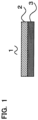
- FIG. 1 is a cross-sectional view of a magnetic shield material according to the present embodiment.
- the magnetic shield material 1 comprises a magnetic layer 2 containing a magnetic material, and an electrically conductive layer 3 containing an electrically conductive material. More specifically, the magnetic shield material 1 is formed by stacking the magnetic layer 2 containing the magnetic material and the electrically conductive layer 3 containing the electrically conductive material.
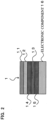
- the electrically conductive layer 3 has a thickness corresponding to a frequency band of an electromagnetic wave to be shielded (electromagnetic wave generated from a device around the magnetic shield material). According to the present embodiment, the thickness of the electrically conductive layer 3 is set to be one which maximizes the magnetic field shield effect of the magnetic shield material 1 in the frequency band of the electromagnetic wave to be shielded.
- Materials which can be used for the magnetic layer 2 described above are: a sheet metal of a high relative permeability metal such as permalloy, silicon steel, iron, stainless steel, sendust or the like which is formed into a sheet shape; a metal foil of an amorphous metal; a ferrite material sintered into a sheet form; and a sheet of each of the magnetic materials described above (the high relative permeability metal such as permalloy, silicon steel, iron and stainless steel, the amorphous metal, and the ferrite material) made by powdering and compounding (mixing) each into resin, rubber or the like.
- each magnetic material used for the magnetic layer 2 is basically a soft magnetic material.
- the soft magnetic material has properties of low coercive force and high relative permeability. Note that in the measurement of magnetic field shield effect described later, a metal foil of a nanocrystalline soft magnetic material produced by crystallizing an amorphous alloy was used for the magnetic layer 2.
- materials which can be used for the electrically conductive layer 3 described above are: a sheet metal of an electrically conductive metal (with low electrical resistivity) such as copper, gold, silver, nickel, aluminum or the like which is formed into a sheet shape; a deposition of each of the electrically conductive metals described above which is made by depositing each on a film, a cloth or the like by a method such as plating, sputtering, vapor deposition or the like so that the (deposition) surface can be used for electrical conduction (current can flow on the surface); and a sheet of each of the electrically conductive metals described above made by powdering and compounding (mixing) each into resin, rubber or the like. Note that in the measurement of magnetic field shield effect described later, an aluminum foil was used for the electrically conductive layer 3.
- the magnetic shield material 1 comprises a layer of PET (polyethylene terephthalate) film 11 and layers of double-sided adhesive tapes 14, 15 in addition to the layers of magnetic foil 12 and aluminum foil 13 described above.
- the lower surface of the PET film 11 is adhered to the upper surface of the magnetic foil 12 by an acrylic resin-based adhesive.
- the reason for providing the layer of PET film 11 on the uppermost layer of magnetic shield material 1 is to protect the surface of the magnetic shield material 1, and to increase heat resistance of the magnetic shield material 1.
- the upper and lower surfaces of the double-sided adhesive tape 14 are attached to the lower surface of the magnetic foil 12 and the upper surface of the aluminum foil 13, respectively, while the upper and lower surfaces of the double-sided adhesive tape 15 are respectively attached to the lower surface of the aluminum foil 13 and the upper surface of the electronic component 16 which acts as an electromagnetic wave (noise) generation source.
- the electronic component 16 includes, of course, a circuit such as an IC as well as a switching power supply.
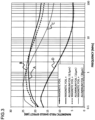
- the magnetic field shield effect of the magnetic shield material 1 was measured by KEC method.
- the KEC method is a measurement method developed by KEC (Kansai Electronic Industry Development Center). According to the measurement system of the KEC method, attenuation of the intensity of magnetic field or electric field of near field in the presence of a shield material as seen from the intensity of magnetic field or electric field of near field (region near magnetic wave generation source) in the absence of the shield material is measured as shield effect in decibels.
- the shield effect (SE) is obtained by the following equation (1).
- SE dB 20 log 10 E 0 / E 1 (where E 0 : magnetic field intensity or electric field intensity of near field in the absence of shield material, E 1 : magnetic field intensity or electric field intensity of near field in the presence of shield material).
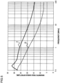
- Curves A, B and C in FIG. 3 are curves showing the measurement results of magnetic field shield effect in the case where the thicknesses of the aluminum foil 13 in the magnetic shield material 1 shown in FIG. 2 are 6.5 ⁇ m, 11 ⁇ m and 30 ⁇ m, respectively.
- curve D in FIG. 3 is a curve showing the measurement result of magnetic field shield effect in the case where the aluminum foil 13 is removed from the magnetic shield material 1 shown in FIG. 2 .
- the magnetic foil 12 of the magnetic shield material 1 used for these measurements had a thickness of 20 ⁇ m and a relative permeability ( ⁇ / ⁇ 0 ) of about 9,000. Note that among the respective layers forming the magnetic shield material 1 shown in FIG.
- a metal foil of a Fe-based nanocrystalline soft magnetic material was used for the magnetic foil 12 of the magnetic shield material 1.
- the composition (weight ratio) of the Fe-based nanocrystalline soft magnetic material was 83 wt% iron (Fe), 9 wt% silicon (Si), 6 wt% niobium (Nb), 1 wt% boron (B) and 1 wt% copper (Cu).
- the measurement system of the KEC method described above can measure magnetic field (or electric field) shield effect of a shield material on electromagnetic waves of various frequencies by changing the frequency from a signal generator.
- the inventor of the present application has found that as shown by curves A, B and C in FIG. 3 , the frequency band (of electromagnetic wave) which makes it possible to obtain a maximum magnetic field shield effect differs (shifts) depending on the thickness of the aluminum foil 13 (electrically conductive layer).
- the inventor of the present application has arrived at a technical concept to maximize the magnetic field shield effect of the magnetic shield material 1 in each frequency band of electromagnetic wave by changing the thickness of the aluminum foil 13 depending on the frequency band of electromagnetic wave to be shielded.
- the frequency (of electromagnetic wave) which enables the magnetic shield material 1 using the aluminum foil 13 with a specific thickness to have a maximum magnetic field shield effect will be referred to as "peak value frequency" (of the magnetic shield material 1 using the aluminum foil 13 with the specific thickness).
- the thicknesses of the respective aluminum foils 13 in the magnetic shield material 1 in the measurements shown in FIG. 3 did not include a thickness (for example, 50 ⁇ m) which is considered to cause the peak value frequency described above to be 0.3 MHz or lower.
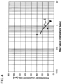
- FIG. 4 is a graph showing change in the peak value frequency described above where the thickness of the aluminum foil 13 in the magnetic shield material 1 shown in FIG. 2 is changed.
- FIG. 4 is a graph showing a correspondence relationship (combination) between the thickness of the aluminum foil 13 and the peak value frequency of the magnetic shield material 1 using the aluminum foil 13 with such thickness.
- curves A, B and C shown in FIG. 3 like curves A, B and C shown in FIG. 3 , only the peak value frequencies where the thicknesses of the aluminum foil 13 are 6.5 ⁇ m, 11 ⁇ m and 30 ⁇ m are plotted.
- curve E of approximate line shown in FIG. 4 is actually obtained by using a lot of measured data for combinations of the thicknesses of the aluminum foil 13 and the peak value frequencies.
- the thickness of the aluminum foil 13 (electrically conductive layer 3) when the intermediate value (average value) of the frequency band of electromagnetic wave to be shielded is equal to the peak value frequency described above is obtained from curve E of approximate line described above, and then the thickness of the aluminum foil 13 in the magnetic shield material 1 is set as the thickness thus obtained from curve E described above. This enables the aluminum foil 13 to have a thickness corresponding to the frequency band of electromagnetic wave to be shielded.
- FIG. 6 the magnetic shield material 1 shown in FIG. 2 is turned upside down, in which the double-sided adhesive tape 15, the aluminum foil 13, the double-sided adhesive tape 14, the magnetic foil 12 and the PET film 11 are stacked in order from top to bottom.
- Curve F shown by the solid line in FIG. 5 is a curve of measurement result of the magnetic field shield effect when, as shown in FIG. 2 , the aluminum foil 13 (electrically conductive layer) is placed on the electronic component 16, and further thereon the magnetic foil 12 (magnetic layer) is placed.
- FIG. 5 is a curve of measurement result of the magnetic field shield effect when, as shown in FIG. 6 , the magnetic foil 12 is placed on the electronic component 16, and further thereon the aluminum foil 13 is placed.
- the aluminum foil 13 with a thickness of 50 ⁇ m was used.
- the magnetic shield material 1 it is possible for the magnetic shield material 1 to have a more significant magnetic field shield effect in the case where the electrically conductive layer (aluminum foil 13) is placed on the electromagnetic wave generation source (electronic component 16), and further thereon the magnetic layer (magnetic foil 12) is placed as shown in FIG. 2 , than in the case where the magnetic layer (magnetic foil 12) is placed on the electromagnetic wave generation source (electronic component 16), and further thereon the electrically conductive layer (aluminum foil 13) is placed as shown in FIG. 6 .
- the aluminum foil 13 (electrically conductive layer 3) is designed to have a thickness corresponding to the frequency band of electromagnetic wave to be shielded.
- the magnetic shield material 1 like the magnetic shield material 1 of the present embodiment, which comprises (has stacked) the magnetic layer 2 containing a magnetic material and the electrically conductive layer 3 containing an electrically conductive material, the thickness of the electrically conductive layer 3 to maximize the magnetic field shield effect differs depending on the frequency band of electromagnetic wave to be shielded.
- the electrically conductive layer 3 (aluminum foil 13) to have a thickness corresponding to the frequency band of electromagnetic wave to be shielded (by changing the thickness of the electrically conductive layer 3 (aluminum foil 13) depending on the frequency band of electromagnetic wave to be shielded), it becomes possible to obtain good magnetic field shield effect in the frequency band of electromagnetic wave to be shielded.
- the thickness of the electrically conductive layer 3 is designed to have a thickness to maximize the magnetic field shield effect of the magnetic shield material 1 in the frequency band of electromagnetic wave to be shielded. This makes it possible to maximize the magnetic field shield effect of the magnetic shield material 1 in the frequency band of electromagnetic wave to be shielded.
- the aluminum foil 13 with high electrical conductivity is used for the electrically conductive layer 3, and therefore, the electromagnetic wave shield capability of the magnetic shield material 1 can be increased.
- a soft magnetic material including Fe-based nanocrystalline soft magnetic material
- the magnetic material of the magnetic layer 2 is used as the magnetic material of the magnetic layer 2, and therefore, the magnetic field shield effect of the magnetic shield material 1 can be increased.
- the thickness of the electrically conductive layer 3 is a thickness to maximize the magnetic field shield effect of the magnetic shield material 1 in a frequency band of electromagnetic wave to be shielded.
- the thickness of the electrically conductive layer is not limited to this, and it is sufficient if it is a thickness corresponding to the frequency band of electromagnetic wave to be shielded (thickness to increase the magnetic field shield effect of the magnetic shield material 1 in the frequency band of electromagnetic wave to be shielded), such embodiment not being covered by the claimed invention.
- FIG. 1 where the magnetic shield material 1 is formed by the magnetic layer 2 and the electrically conductive layer 3, and an example in FIG. 2 where the magnetic shield material 1 is formed by the PET film 11, the magnetic layer (magnetic foil 12), the double-sided adhesive tapes 14, 15 and the electrically conductive layer (aluminum foil 13).
- the structure of the magnetic shield material of the present invention it is sufficient if it is a structure comprising a magnetic layer containing a magnetic material and an electrically conductive layer containing an electrically conductive material, as long as it falls within the limitations of the appended claims.
Landscapes
- Engineering & Computer Science (AREA)
- Microelectronics & Electronic Packaging (AREA)
- Physics & Mathematics (AREA)
- Electromagnetism (AREA)
- Life Sciences & Earth Sciences (AREA)
- Wood Science & Technology (AREA)
- Shielding Devices Or Components To Electric Or Magnetic Fields (AREA)
- Laminated Bodies (AREA)
Applications Claiming Priority (2)
| Application Number | Priority Date | Filing Date | Title |
|---|---|---|---|
| JP2018216845A JP7207706B2 (ja) | 2018-11-19 | 2018-11-19 | 磁気シールド材 |
| PCT/JP2019/044731 WO2020105543A1 (ja) | 2018-11-19 | 2019-11-14 | 磁気シールド材 |
Publications (3)
| Publication Number | Publication Date |
|---|---|
| EP3886550A1 EP3886550A1 (en) | 2021-09-29 |
| EP3886550A4 EP3886550A4 (en) | 2021-12-22 |
| EP3886550B1 true EP3886550B1 (en) | 2025-06-18 |
Family
ID=70774495
Family Applications (1)
| Application Number | Title | Priority Date | Filing Date |
|---|---|---|---|
| EP19887297.0A Active EP3886550B1 (en) | 2018-11-19 | 2019-11-14 | Magnetic shield material |
Country Status (5)
| Country | Link |
|---|---|
| US (1) | US11690207B2 (enExample) |
| EP (1) | EP3886550B1 (enExample) |
| JP (1) | JP7207706B2 (enExample) |
| CN (1) | CN112740848B (enExample) |
| WO (1) | WO2020105543A1 (enExample) |
Families Citing this family (6)
| Publication number | Priority date | Publication date | Assignee | Title |
|---|---|---|---|---|
| US12064250B2 (en) * | 2020-12-28 | 2024-08-20 | Biosense Webster (Israel) Ltd. | Generic box for electrophysiology system adapters |
| JP2022153032A (ja) * | 2021-03-29 | 2022-10-12 | Jx金属株式会社 | 積層体及びその製造方法 |
| KR102586948B1 (ko) * | 2021-04-02 | 2023-10-10 | 주식회사 아모센스 | 자기장 차폐시트 및 이의 제조방법 |
| JP7627247B2 (ja) * | 2022-07-20 | 2025-02-07 | Jx金属株式会社 | 電磁波遮蔽材料、被覆材又は外装材及び電気・電子機器 |
| CN115484808A (zh) * | 2022-10-17 | 2022-12-16 | 宁波中科毕普拉斯新材料科技有限公司 | 一种电磁屏蔽复合材料及制备方法 |
| JPWO2024117012A1 (enExample) * | 2022-11-28 | 2024-06-06 |
Citations (3)
| Publication number | Priority date | Publication date | Assignee | Title |
|---|---|---|---|---|
| CN101704312A (zh) * | 2009-11-06 | 2010-05-12 | 电子科技大学 | 复合电磁屏蔽材料及其制造方法 |
| US20160057901A1 (en) * | 2014-08-25 | 2016-02-25 | Chase Corporation | Paper/ plastic laminate and electromagnetic shielding material |
| CN205454370U (zh) * | 2015-12-24 | 2016-08-10 | 上海光线新材料科技有限公司 | 一种电磁屏蔽复合材料 |
Family Cites Families (8)
| Publication number | Priority date | Publication date | Assignee | Title |
|---|---|---|---|---|
| US5260128A (en) * | 1989-12-11 | 1993-11-09 | Kabushiki Kaisha Riken | Electromagnetic shielding sheet |
| JP3900559B2 (ja) * | 1996-09-19 | 2007-04-04 | 大同特殊鋼株式会社 | 磁気遮蔽用シートとその製造方法及びこれを用いたケーブル |
| FI20020025A0 (fi) * | 2002-01-08 | 2002-01-08 | 4 D Neuroimaging Oy | Komposiittiseinõrakenne parannetun magneettisuojauksen aikaansaamiseksi |
| JP2005142551A (ja) * | 2003-10-17 | 2005-06-02 | Nitta Ind Corp | 磁気シールドシートおよび入力対応表示装置 |
| JP2010153542A (ja) * | 2008-12-25 | 2010-07-08 | Ado Union Kenkyusho:Kk | 電磁波抑制シート及びその製造方法 |
| CN105935009A (zh) * | 2014-03-14 | 2016-09-07 | 株式会社钟化 | 电子终端设备及其组装方法 |
| JP2018067629A (ja) | 2016-10-19 | 2018-04-26 | 京セラ株式会社 | 電磁波シールド用積層接着シートおよびその接着方法 |
| CN107864604A (zh) * | 2017-11-10 | 2018-03-30 | 中国科学院西安光学精密机械研究所 | 一种电磁辐射屏蔽结构 |
-
2018
- 2018-11-19 JP JP2018216845A patent/JP7207706B2/ja active Active
-
2019
- 2019-11-14 CN CN201980062317.9A patent/CN112740848B/zh active Active
- 2019-11-14 EP EP19887297.0A patent/EP3886550B1/en active Active
- 2019-11-14 US US17/294,873 patent/US11690207B2/en active Active
- 2019-11-14 WO PCT/JP2019/044731 patent/WO2020105543A1/ja not_active Ceased
Patent Citations (3)
| Publication number | Priority date | Publication date | Assignee | Title |
|---|---|---|---|---|
| CN101704312A (zh) * | 2009-11-06 | 2010-05-12 | 电子科技大学 | 复合电磁屏蔽材料及其制造方法 |
| US20160057901A1 (en) * | 2014-08-25 | 2016-02-25 | Chase Corporation | Paper/ plastic laminate and electromagnetic shielding material |
| CN205454370U (zh) * | 2015-12-24 | 2016-08-10 | 上海光线新材料科技有限公司 | 一种电磁屏蔽复合材料 |
Also Published As
| Publication number | Publication date |
|---|---|
| US20220007555A1 (en) | 2022-01-06 |
| CN112740848A (zh) | 2021-04-30 |
| WO2020105543A1 (ja) | 2020-05-28 |
| CN112740848B (zh) | 2024-07-09 |
| JP7207706B2 (ja) | 2023-01-18 |
| EP3886550A1 (en) | 2021-09-29 |
| US11690207B2 (en) | 2023-06-27 |
| EP3886550A4 (en) | 2021-12-22 |
| JP2020088045A (ja) | 2020-06-04 |
Similar Documents
| Publication | Publication Date | Title |
|---|---|---|
| EP3886550B1 (en) | Magnetic shield material | |
| CN104885587B (zh) | 电磁波吸收板及其制造方法和包含其的电子设备 | |
| CN109671551B (zh) | 电感部件 | |
| US8399964B2 (en) | Multilayer structures for magnetic shielding | |
| KR102359198B1 (ko) | 노이즈 억제 조립체 | |
| KR20170142974A (ko) | 인덕터 및 이의 제조방법 | |
| JP2007514321A (ja) | ミックスド・シグナル集積回路のための低クロストーク回路基板 | |
| US11881342B2 (en) | Coil electronic component | |
| US11516951B2 (en) | Noise suppression sheet | |
| KR100868838B1 (ko) | 배선 기판, 전자 기기 및 전원 장치 | |
| US12238912B2 (en) | Electromagnetic energy mitigation assemblies and automotive vehicle components including the same | |
| US11613100B2 (en) | Noise suppression sheet | |
| US11419250B2 (en) | Noise suppression sheet | |
| JP2003115691A (ja) | フィルム状emiフィルタ | |
| Duhni et al. | Bi-Layered Magnetic Electromagnetic Interference Shields with Thinner Metals | |
| EP4344373A1 (en) | Electromagnetic energy mitigation assemblies and automotive vehicle components incluing the same | |
| CN113543613A (zh) | 噪声抑制薄片 | |
| JP2025076205A (ja) | シールド材 | |
| WO2022255023A1 (ja) | 電磁波シールド材、電子部品および電子機器 | |
| JP2005116763A (ja) | 軟磁性部材、軟磁性部材の製造方法及び電子機器 |
Legal Events
| Date | Code | Title | Description |
|---|---|---|---|
| STAA | Information on the status of an ep patent application or granted ep patent |
Free format text: STATUS: THE INTERNATIONAL PUBLICATION HAS BEEN MADE |
|
| PUAI | Public reference made under article 153(3) epc to a published international application that has entered the european phase |
Free format text: ORIGINAL CODE: 0009012 |
|
| STAA | Information on the status of an ep patent application or granted ep patent |
Free format text: STATUS: REQUEST FOR EXAMINATION WAS MADE |
|
| 17P | Request for examination filed |
Effective date: 20210602 |
|
| AK | Designated contracting states |
Kind code of ref document: A1 Designated state(s): AL AT BE BG CH CY CZ DE DK EE ES FI FR GB GR HR HU IE IS IT LI LT LU LV MC MK MT NL NO PL PT RO RS SE SI SK SM TR |
|
| A4 | Supplementary search report drawn up and despatched |
Effective date: 20211123 |
|
| RIC1 | Information provided on ipc code assigned before grant |
Ipc: B32B 7/025 20190101ALI20211117BHEP Ipc: H05K 9/00 20060101AFI20211117BHEP |
|
| DAV | Request for validation of the european patent (deleted) | ||
| DAX | Request for extension of the european patent (deleted) | ||
| STAA | Information on the status of an ep patent application or granted ep patent |
Free format text: STATUS: EXAMINATION IS IN PROGRESS |
|
| 17Q | First examination report despatched |
Effective date: 20231220 |
|
| GRAP | Despatch of communication of intention to grant a patent |
Free format text: ORIGINAL CODE: EPIDOSNIGR1 |
|
| STAA | Information on the status of an ep patent application or granted ep patent |
Free format text: STATUS: GRANT OF PATENT IS INTENDED |
|
| INTG | Intention to grant announced |
Effective date: 20250318 |
|
| GRAS | Grant fee paid |
Free format text: ORIGINAL CODE: EPIDOSNIGR3 |
|
| GRAA | (expected) grant |
Free format text: ORIGINAL CODE: 0009210 |
|
| STAA | Information on the status of an ep patent application or granted ep patent |
Free format text: STATUS: THE PATENT HAS BEEN GRANTED |
|
| AK | Designated contracting states |
Kind code of ref document: B1 Designated state(s): AL AT BE BG CH CY CZ DE DK EE ES FI FR GB GR HR HU IE IS IT LI LT LU LV MC MK MT NL NO PL PT RO RS SE SI SK SM TR |
|
| REG | Reference to a national code |
Ref country code: GB Ref legal event code: FG4D |
|
| REG | Reference to a national code |
Ref country code: CH Ref legal event code: EP |
|
| REG | Reference to a national code |
Ref country code: DE Ref legal event code: R096 Ref document number: 602019071387 Country of ref document: DE |
|
| REG | Reference to a national code |
Ref country code: CH Ref legal event code: EP |
|
| REG | Reference to a national code |
Ref country code: IE Ref legal event code: FG4D |
|
| PG25 | Lapsed in a contracting state [announced via postgrant information from national office to epo] |
Ref country code: FI Free format text: LAPSE BECAUSE OF FAILURE TO SUBMIT A TRANSLATION OF THE DESCRIPTION OR TO PAY THE FEE WITHIN THE PRESCRIBED TIME-LIMIT Effective date: 20250618 |
|
| REG | Reference to a national code |
Ref country code: LT Ref legal event code: MG9D |
|
| PG25 | Lapsed in a contracting state [announced via postgrant information from national office to epo] |
Ref country code: NO Free format text: LAPSE BECAUSE OF FAILURE TO SUBMIT A TRANSLATION OF THE DESCRIPTION OR TO PAY THE FEE WITHIN THE PRESCRIBED TIME-LIMIT Effective date: 20250918 Ref country code: GR Free format text: LAPSE BECAUSE OF FAILURE TO SUBMIT A TRANSLATION OF THE DESCRIPTION OR TO PAY THE FEE WITHIN THE PRESCRIBED TIME-LIMIT Effective date: 20250919 |
|
| PG25 | Lapsed in a contracting state [announced via postgrant information from national office to epo] |
Ref country code: BG Free format text: LAPSE BECAUSE OF FAILURE TO SUBMIT A TRANSLATION OF THE DESCRIPTION OR TO PAY THE FEE WITHIN THE PRESCRIBED TIME-LIMIT Effective date: 20250618 |
|
| PG25 | Lapsed in a contracting state [announced via postgrant information from national office to epo] |
Ref country code: HR Free format text: LAPSE BECAUSE OF FAILURE TO SUBMIT A TRANSLATION OF THE DESCRIPTION OR TO PAY THE FEE WITHIN THE PRESCRIBED TIME-LIMIT Effective date: 20250618 |
|
| PG25 | Lapsed in a contracting state [announced via postgrant information from national office to epo] |
Ref country code: RS Free format text: LAPSE BECAUSE OF FAILURE TO SUBMIT A TRANSLATION OF THE DESCRIPTION OR TO PAY THE FEE WITHIN THE PRESCRIBED TIME-LIMIT Effective date: 20250918 |
|
| REG | Reference to a national code |
Ref country code: NL Ref legal event code: MP Effective date: 20250618 |
|
| PG25 | Lapsed in a contracting state [announced via postgrant information from national office to epo] |
Ref country code: LV Free format text: LAPSE BECAUSE OF FAILURE TO SUBMIT A TRANSLATION OF THE DESCRIPTION OR TO PAY THE FEE WITHIN THE PRESCRIBED TIME-LIMIT Effective date: 20250618 |
|
| PG25 | Lapsed in a contracting state [announced via postgrant information from national office to epo] |
Ref country code: NL Free format text: LAPSE BECAUSE OF FAILURE TO SUBMIT A TRANSLATION OF THE DESCRIPTION OR TO PAY THE FEE WITHIN THE PRESCRIBED TIME-LIMIT Effective date: 20250618 |
|
| PG25 | Lapsed in a contracting state [announced via postgrant information from national office to epo] |
Ref country code: PT Free format text: LAPSE BECAUSE OF FAILURE TO SUBMIT A TRANSLATION OF THE DESCRIPTION OR TO PAY THE FEE WITHIN THE PRESCRIBED TIME-LIMIT Effective date: 20251020 |
|
| REG | Reference to a national code |
Ref country code: AT Ref legal event code: MK05 Ref document number: 1805416 Country of ref document: AT Kind code of ref document: T Effective date: 20250618 |
|
| PG25 | Lapsed in a contracting state [announced via postgrant information from national office to epo] |
Ref country code: IS Free format text: LAPSE BECAUSE OF FAILURE TO SUBMIT A TRANSLATION OF THE DESCRIPTION OR TO PAY THE FEE WITHIN THE PRESCRIBED TIME-LIMIT Effective date: 20251018 |
|
| PGFP | Annual fee paid to national office [announced via postgrant information from national office to epo] |
Ref country code: DE Payment date: 20251119 Year of fee payment: 7 |
|
| PG25 | Lapsed in a contracting state [announced via postgrant information from national office to epo] |
Ref country code: AT Free format text: LAPSE BECAUSE OF FAILURE TO SUBMIT A TRANSLATION OF THE DESCRIPTION OR TO PAY THE FEE WITHIN THE PRESCRIBED TIME-LIMIT Effective date: 20250618 Ref country code: SM Free format text: LAPSE BECAUSE OF FAILURE TO SUBMIT A TRANSLATION OF THE DESCRIPTION OR TO PAY THE FEE WITHIN THE PRESCRIBED TIME-LIMIT Effective date: 20250618 |
|
| PGFP | Annual fee paid to national office [announced via postgrant information from national office to epo] |
Ref country code: FR Payment date: 20251126 Year of fee payment: 7 |
|
| PG25 | Lapsed in a contracting state [announced via postgrant information from national office to epo] |
Ref country code: CZ Free format text: LAPSE BECAUSE OF FAILURE TO SUBMIT A TRANSLATION OF THE DESCRIPTION OR TO PAY THE FEE WITHIN THE PRESCRIBED TIME-LIMIT Effective date: 20250618 |
|
| PG25 | Lapsed in a contracting state [announced via postgrant information from national office to epo] |
Ref country code: PL Free format text: LAPSE BECAUSE OF FAILURE TO SUBMIT A TRANSLATION OF THE DESCRIPTION OR TO PAY THE FEE WITHIN THE PRESCRIBED TIME-LIMIT Effective date: 20250618 |
|
| PG25 | Lapsed in a contracting state [announced via postgrant information from national office to epo] |
Ref country code: EE Free format text: LAPSE BECAUSE OF FAILURE TO SUBMIT A TRANSLATION OF THE DESCRIPTION OR TO PAY THE FEE WITHIN THE PRESCRIBED TIME-LIMIT Effective date: 20250618 |
|
| PG25 | Lapsed in a contracting state [announced via postgrant information from national office to epo] |
Ref country code: RO Free format text: LAPSE BECAUSE OF FAILURE TO SUBMIT A TRANSLATION OF THE DESCRIPTION OR TO PAY THE FEE WITHIN THE PRESCRIBED TIME-LIMIT Effective date: 20250618 Ref country code: SK Free format text: LAPSE BECAUSE OF FAILURE TO SUBMIT A TRANSLATION OF THE DESCRIPTION OR TO PAY THE FEE WITHIN THE PRESCRIBED TIME-LIMIT Effective date: 20250618 |
|
| PG25 | Lapsed in a contracting state [announced via postgrant information from national office to epo] |
Ref country code: ES Free format text: LAPSE BECAUSE OF FAILURE TO SUBMIT A TRANSLATION OF THE DESCRIPTION OR TO PAY THE FEE WITHIN THE PRESCRIBED TIME-LIMIT Effective date: 20250618 |
|
| PG25 | Lapsed in a contracting state [announced via postgrant information from national office to epo] |
Ref country code: DK Free format text: LAPSE BECAUSE OF FAILURE TO SUBMIT A TRANSLATION OF THE DESCRIPTION OR TO PAY THE FEE WITHIN THE PRESCRIBED TIME-LIMIT Effective date: 20250618 |
|
| PG25 | Lapsed in a contracting state [announced via postgrant information from national office to epo] |
Ref country code: IT Free format text: LAPSE BECAUSE OF FAILURE TO SUBMIT A TRANSLATION OF THE DESCRIPTION OR TO PAY THE FEE WITHIN THE PRESCRIBED TIME-LIMIT Effective date: 20250618 |
|
| PLBE | No opposition filed within time limit |
Free format text: ORIGINAL CODE: 0009261 |
|
| STAA | Information on the status of an ep patent application or granted ep patent |
Free format text: STATUS: NO OPPOSITION FILED WITHIN TIME LIMIT |
|
| REG | Reference to a national code |
Ref country code: CH Ref legal event code: L10 Free format text: ST27 STATUS EVENT CODE: U-0-0-L10-L00 (AS PROVIDED BY THE NATIONAL OFFICE) Effective date: 20260430 |