EP3884893A1 - Medizingerät mit einem betriebssicheren netzteil - Google Patents
Medizingerät mit einem betriebssicheren netzteil Download PDFInfo
- Publication number
- EP3884893A1 EP3884893A1 EP21163547.9A EP21163547A EP3884893A1 EP 3884893 A1 EP3884893 A1 EP 3884893A1 EP 21163547 A EP21163547 A EP 21163547A EP 3884893 A1 EP3884893 A1 EP 3884893A1
- Authority
- EP
- European Patent Office
- Prior art keywords
- voltage
- medical device
- capacitor
- power supply
- transistor
- Prior art date
- Legal status (The legal status is an assumption and is not a legal conclusion. Google has not performed a legal analysis and makes no representation as to the accuracy of the status listed.)
- Granted
Links
Images


Classifications
-
- A—HUMAN NECESSITIES
- A61—MEDICAL OR VETERINARY SCIENCE; HYGIENE
- A61B—DIAGNOSIS; SURGERY; IDENTIFICATION
- A61B18/00—Surgical instruments, devices or methods for transferring non-mechanical forms of energy to or from the body
- A61B18/04—Surgical instruments, devices or methods for transferring non-mechanical forms of energy to or from the body by heating
- A61B18/08—Surgical instruments, devices or methods for transferring non-mechanical forms of energy to or from the body by heating by means of electrically-heated probes
- A61B18/10—Power sources therefor
-
- H—ELECTRICITY
- H02—GENERATION; CONVERSION OR DISTRIBUTION OF ELECTRIC POWER
- H02M—APPARATUS FOR CONVERSION BETWEEN AC AND AC, BETWEEN AC AND DC, OR BETWEEN DC AND DC, AND FOR USE WITH MAINS OR SIMILAR POWER SUPPLY SYSTEMS; CONVERSION OF DC OR AC INPUT POWER INTO SURGE OUTPUT POWER; CONTROL OR REGULATION THEREOF
- H02M1/00—Details of apparatus for conversion
- H02M1/32—Means for protecting converters other than automatic disconnection
- H02M1/322—Means for rapidly discharging a capacitor of the converter for protecting electrical components or for preventing electrical shock
-
- H—ELECTRICITY
- H02—GENERATION; CONVERSION OR DISTRIBUTION OF ELECTRIC POWER
- H02J—ELECTRIC POWER NETWORKS; CIRCUIT ARRANGEMENTS OR SYSTEMS FOR SUPPLYING OR DISTRIBUTING ELECTRIC POWER; SYSTEMS FOR STORING ELECTRIC ENERGY
- H02J7/00—Circuit arrangements for charging or discharging batteries or for supplying loads from batteries
- H02J7/60—Circuit arrangements for charging or discharging batteries or for supplying loads from batteries including safety or protection arrangements
-
- H—ELECTRICITY
- H02—GENERATION; CONVERSION OR DISTRIBUTION OF ELECTRIC POWER
- H02M—APPARATUS FOR CONVERSION BETWEEN AC AND AC, BETWEEN AC AND DC, OR BETWEEN DC AND DC, AND FOR USE WITH MAINS OR SIMILAR POWER SUPPLY SYSTEMS; CONVERSION OF DC OR AC INPUT POWER INTO SURGE OUTPUT POWER; CONTROL OR REGULATION THEREOF
- H02M1/00—Details of apparatus for conversion
- H02M1/32—Means for protecting converters other than automatic disconnection
-
- H—ELECTRICITY
- H02—GENERATION; CONVERSION OR DISTRIBUTION OF ELECTRIC POWER
- H02J—ELECTRIC POWER NETWORKS; CIRCUIT ARRANGEMENTS OR SYSTEMS FOR SUPPLYING OR DISTRIBUTING ELECTRIC POWER; SYSTEMS FOR STORING ELECTRIC ENERGY
- H02J2105/00—Networks for supplying or distributing electric power characterised by their spatial reach or by the load
- H02J2105/40—Networks for supplying or distributing electric power characterised by their spatial reach or by the load characterised by the loads connecting to the networks or being supplied by the networks
- H02J2105/46—Medical devices, medical implants or life supporting devices
-
- H—ELECTRICITY
- H02—GENERATION; CONVERSION OR DISTRIBUTION OF ELECTRIC POWER
- H02J—ELECTRIC POWER NETWORKS; CIRCUIT ARRANGEMENTS OR SYSTEMS FOR SUPPLYING OR DISTRIBUTING ELECTRIC POWER; SYSTEMS FOR STORING ELECTRIC ENERGY
- H02J2207/00—Details of circuit arrangements for charging or discharging batteries or supplying loads from batteries
- H02J2207/50—Charging of capacitors, supercapacitors, ultra-capacitors or double layer capacitors
Definitions
- the invention relates to a medical device with a power supply unit for connection to an alternating current network, the power supply unit having a rectifier and at least one filter capacitor for smoothing a DC voltage to be output by the power supply unit, as well as at least one discharge resistor for discharging the filter capacitor.
- the invention relates in particular to an electrosurgical generator with outputs to which an electrosurgical instrument can be connected and via which a connected electrosurgical instrument can be supplied with a high-frequency AC output voltage.
- capacitors of an electrical device should no longer be connected to a higher voltage within a reasonable time after it has been switched off.
- This also applies to medical devices and, in particular, high-voltage DC power supplies for electrosurgical generators.
- discharge resistors are provided that are parallel to high-capacity capacitors and discharge them.
- the invention is based on the object of creating an improved power supply, in particular for a medical device such as an electrosurgery generator, which fulfills the safety requirements.
- a medical device with a power supply unit for connection to an alternating current network, which has a circuit to connect at least one discharge resistor in parallel with at least one filter capacitor only when no AC input voltage is applied to the power supply unit.
- the power supply unit has a rectifier and at least one filter capacitor for smoothing a DC voltage to be output by the power supply unit, as well as at least one discharge resistor for discharging the filter capacitor.
- the power supply unit has a circuit which is electrically connected to the discharge resistor and the filter capacitor and which is designed to detect a switched-on state of the medical device in which an AC input voltage is applied to the power supply unit and only then to apply the discharge resistor in parallel with the filter capacitor switch if the circuit does not detect a switched-on state of the medical device.
- the circuit has a first transistor (T2) for connecting the discharge resistor (R4, R5, R6, R7, R8, R9) in parallel to the filter capacitor (C1).
- the first transistor (T2) is arranged and dimensioned in such a way that it switches through and causes the filter capacitor (C1) to discharge when a capacitor (C4) connected to the base or the gate of the first transistor (T2) and serving as a control capacitor is sufficiently charged is.
- the capacitor (C4) is regularly discharged by means of a second transistor (T1), which serves as a control transistor, as long as the power supply unit is supplied with mains voltage.
- the AC input voltage can thus be detected reliably over the entire input voltage range of the medical device and the additional energy required to supply the detection circuit is minimized.
- the circuit preferably has a switch for connecting the discharge resistor in parallel to the filter capacitor.
- the switch is preferably a field effect transistor.
- a power supply unit with an electronic circuit which only then has one or more discharge resistors in parallel with one or more corresponding ones Capacitors of the power supply unit - especially filter capacitors - switch when the medical device is switched off.
- the supply voltage (alternating voltage) is detected and used as a control variable.
- the invention includes the knowledge that, depending on the voltage value and capacity of the filter capacitors, more or less high currents flow through these discharge resistors.
- B. an electrosurgery generator in standby mode increased significantly. This increases the internal temperature of the medical device and reduces the mean operating time between failures of the medical device.
- the rectifier preferably has a rectifier bridge, and the circuit is preferably configured to tap a voltage between an input-side connection of the rectifier bridge and an output-side connection of the rectifier bridge and to detect a supply network voltage applied to the input-side connection of the rectifier bridge.
- the circuit preferably has a voltage divider connected between an input of the rectifier bridge and the negative output of the rectifier bridge and a first capacitor connected in parallel with a resistor of the voltage divider, which filters any interference pulses that may occur on the network side in the event of a supply network voltage and for the necessary division ratio of the voltage divider cares.
- the base-emitter path of the control transistor is preferably connected in parallel to the resistor of the voltage divider and the control transistor switches through in the event of a supply network voltage in the range of> 50 V AC ... 264 V AC in time with the AC input voltage.
- the control transistor is thus preferably operated in an emitter circuit.
- the control transistor is preferably a bipolar transistor, in particular an npn transistor.
- the control transistor can, however, also be a pnp transistor and the circuit can be constructed in a correspondingly complementary manner. Alternatively, a corresponding circuit with a field effect transistor is also possible.
- a second capacitor is preferably connected in parallel to a gate-drain path of the field effect transistor serving as a switch. In its charged state, this second capacitor has the effect that the field effect transistor switches through, so that the at least one discharge resistor is connected in parallel to the at least one filter capacitor is.
- the second capacitor is charged from the filter capacitor when no mains voltage is applied to the rectifier or its rectifier bridge and causes the field effect transistor serving as a switch to switch through and thus the at least one discharge resistor is connected in parallel to the at least one filter capacitor. In this way, the filter capacitor is discharged via the discharge resistor when there is no mains voltage applied to an input of the rectifier.
- the second capacitor is preferably connected in parallel to a collector-emitter path of the control transistor, so that the second capacitor is discharged when the control transistor is switched on.
- the field effect transistor serving as a switch blocks so that the at least one discharge resistor is separated from the at least one filter capacitor.
- the control transistor switches through when a supply network voltage is applied to the input of the rectifier and thus has the effect that the discharge resistor is separated from the filter capacitor when the supply network voltage is applied.
- the circuit preferably has one or more Zener diodes for voltage limitation.
- a respective Zener diode is provided in particular to protect a respective transistor.
- the circuit preferably has a plurality of discharge resistors connected in parallel with one another, in order in this way to enable greater power dissipation when discharging the filter capacitor.
- the at least one discharge resistor preferably has a resistance value between 47 k ⁇ and 120 k ⁇ .
- the resistance value of the discharge resistor should preferably be selected such that 60 seconds after the maximum AC input voltage has been switched off, the DC voltage across the at least one filter capacitor has dropped to less than 60V.
- the preferred resistance value of the at least one discharge resistor thus results from the maximum AC input voltage and the capacitance of the at least one filter capacitor.
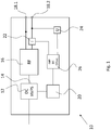
- FIG 1 shows a medical device using the example of an electrosurgery generator 10.
- the high-voltage direct current is fed to a high-frequency part 16 of the electrosurgical generator 10.
- the high-frequency part 16 of the electrosurgery generator 10 acts as an inverter and generates a high-frequency alternating voltage that is output via an output transformer (not shown) of the high-frequency part 16 to outputs 18.1 and 18.2 of the electrosurgery generator 10.
- An electrosurgical instrument can be connected to the outputs 18.1 and 18.2 of the electrosurgical generator 10.
- the output power of the electrosurgery generator 10 can be controlled or regulated by means of a control unit 20 and acquisition units 22 and 24 as well as an evaluation unit 26 for forming values such as impedance etc. derived from acquired values.
- the mains input voltage is converted into a variable DC voltage. This serves as an input voltage for an inverter circuit of the high-voltage power supply 12, the output voltage of which increases proportionally to the input voltage.
- the output voltage (and thus also the current and power) can therefore be regulated with the help of the input voltage.
- Figure 2 shows an example of a high-voltage power supply according to the invention.
- the supply voltage (alternating voltage) is detected and used as a control variable.
- the prerequisite is that the device is operated with a supply voltage between 100 and 240 VAC.
- a power supply unit for generating an output DC voltage from an input AC voltage typically has a rectifier bridge formed by four diodes for rectifying the AC current and one or more filter capacitors for smoothing the output DC voltage.
- the rectifier bridge has two inputs for the AC input voltage and two outputs for the DC output voltage. One output is positive, the other output of the rectifier bridge is negative.
- a filter capacitor C1 is provided in the form of an electrolytic capacitor with a capacity of 2000 ⁇ F.
- several filter capacitors connected in parallel or in series can also be provided. If the DC output voltage of the high-voltage power supply is, for example, 300 V, the filter capacitors can be connected in series in pairs, so that only a maximum voltage of 150 V is dropped across each of the filter capacitors.
- the filter capacitance can be increased by connecting the filter capacitors in parallel.
- each of the resistors R4 to R9 has a resistance of 68 k ⁇ .
- the 6 discharge resistors R4 to R9 are connected in parallel to the filter capacitor C1.
- the number and dimensioning of the discharge resistors is generally in relation to the The capacitance of the filter capacitors and the maximum voltage are preferably selected so that the discharge resistors allow a discharge power that is required to reduce the maximum voltage across the capacitors to below 60 V in a maximum of 60 seconds.
- the 6 discharge resistors R4 to R9 do not continuously dissipate power even when the medical device is switched on, they are separated from the filter capacitor C1 when the medical device is switched on.
- a field effect transistor T2 which serves as a switch, is used for this purpose.
- the field effect transistor T2 is controlled by a detection circuit which is designed to detect the presence of an input AC voltage and only then to switch the field effect transistor through - and thus to connect the 6 discharge resistors R4 to R9 in parallel to the filter capacitor C1 - when there is no input AC voltage on the power supply unit of the medical device is present.
- the detection circuit To detect the supply voltage and to control the field effect transistor T2, the detection circuit has resistors R1 (1 M ⁇ ) and R2 (100 k ⁇ ) and a capacitor C2 (10nF), which are connected in series between an input of the rectifier bridge and the negative output of the rectifier bridge are.
- a capacitor C3 (10 nF) is connected in parallel to the resistor R2.
- the voltage is tapped between the capacitor C2 and the resistor R2 and fed to the base of an npn transistor T1.
- the transistor T1 is thus a bipolar transistor which is operated in an emitter circuit and serves as a control transistor which, when switched on, causes a capacitor C4 to discharge.
- the capacitor C4 is connected in parallel to the filter capacitor C1 and is charged by the filter capacitor C1 via a resistor R3 connected in series with the capacitor C4 if the transistor T1 is not turned on.
- the AC voltage is decoupled via the resistor R1 and the capacitor C2 before the rectification and filtered by the resistor R2 and the capacitor C3 and reduced so that it can be processed by the transistor T1 (an npn transistor).
- the transistor T1 an npn transistor
- the transistor T1 is switched through in time with the alternating voltage and thus prevents the capacitor C4 from being able to charge via the resistor R3.
- the transistor T2 remains blocked and the discharge resistors are de-energized.
- Zener diodes D1 (3.3 V) and D2 (10 V) each limit the voltage.
- the Zener diode D1 is connected in parallel to the resistor R2, the capacitor C3 and the base-emitter path of the transistor T1.
- the Zener-Dide D2 and a capacitor C4 (1 ⁇ F) are connected in parallel to the collector-emitter path of the transistor T1.
- the resistor R3 and the capacitor C4 are connected in series with one another between the two outputs of the rectifier bridge and parallel to the filter capacitor C1.
- the resistor R3 determines how fast the capacitor C4 is charged and thus serves as a timer.
- the Zener diode D2 limits the voltage across the capacitor C4 to a maximum of 10 volts. The capacitor C4 can thus be charged to a maximum of 10 volts.
- the gate of the field effect transistor T2 is controlled via the voltage across the capacitor C4.
- the transistor T1 blocks and the capacitor C4 (1 ⁇ F) can be charged up to 10 V via the resistor R3.
- the field effect transistor T2 thus becomes conductive and the discharge resistors R4 to R9 discharge the filter capacitor C1.
- the capacitor C4 is discharged via the transistor T1 and the field effect transistor T2 blocks.
- the discharge resistors R4 to R9 are thus de-energized again.
- Figure 3 shows a circuit for a power supply unit for generating a symmetrical DC output voltage.
- the circuit is largely a duplication of the in Figure 2 shown circuit.
- the two additional resistors R10 and R20 are used to balance the DC voltage on the filter electrolytic capacitors. If the DC voltage between positive output DC voltage + UDC and negative output DC voltage -UDC is not loaded against ground MP_GND, different high leakage currents in the capacitors could result in asymmetrically high voltages against ground MP_GND if the AC supply voltage is available and the discharge resistors are not switched on are.
- R10 and R20 are preferably dimensioned so that they carry approximately five times the leakage current of the capacitors,
- the circuit is designed for a supply voltage (alternating voltage at the input of the rectifier bridge) between 100 and 240 VAC.
Landscapes
- Engineering & Computer Science (AREA)
- Power Engineering (AREA)
- Health & Medical Sciences (AREA)
- Surgery (AREA)
- Life Sciences & Earth Sciences (AREA)
- Heart & Thoracic Surgery (AREA)
- Molecular Biology (AREA)
- Nuclear Medicine, Radiotherapy & Molecular Imaging (AREA)
- Plasma & Fusion (AREA)
- Biomedical Technology (AREA)
- Physics & Mathematics (AREA)
- Medical Informatics (AREA)
- Otolaryngology (AREA)
- Animal Behavior & Ethology (AREA)
- General Health & Medical Sciences (AREA)
- Public Health (AREA)
- Veterinary Medicine (AREA)
- Rectifiers (AREA)
- Surgical Instruments (AREA)
- Direct Current Feeding And Distribution (AREA)
Abstract
Description
- Die Erfindung betrifft ein Medizingerät mit einem Netzteil zum Anschluss an ein Wechselstromnetz, wobei das Netzteil einen Gleichrichter und wenigstens einen Siebkondensator zum Glätten einer von dem Netzteil auszugebenden Gleichspannung sowie wenigstens einen Entladewiderstand zum Entladen des Siebkondensators aufweist. Die Erfindung betrifft insbesondere einen Elektrochirurgie-Generator mit Ausgängen, an die ein elektrochirurgisches Instrument angeschlossen und über die ein angeschlossenes elektrochirurgisches Instrument mit einer hochfrequenten Ausgangswechselspannung versorgt werden kann.
- Aus Sicherheitsgründen soll an Kondensatoren eines elektrischen Geräts in angemessener Zeit nach dessen Ausschalten keine höhere Spannung mehr anliegen. Dies betrifft auch Medizingeräte und insbesondere Hochspannungsgleichstromnetzteile von Elektrochirurgie-Generatoren. Zu diesem Zweck sind Entladewiderstände vorgesehen, die parallel zu hochkapazitiven Kondensatoren liegen und diese entladen.
- Aus dem
US-Patent 5,523,665 A ist ein Netzteil mit einer Gleichrichterbrücke und Siebkondensatoren bekannt, die nach dem Wegfall der Netzspannung über einen Widerstand entladen werden. - Der Erfindung liegt die Aufgabe zugrunde, ein verbessertes Netzteil insbesondere für ein Medizingerät wie einen Elektrochirurgie-Generator zu schaffen, welches die Sicherheitsanforderungen erfüllt.
- Erfindungsgemäß wird diese Aufgabe durch ein Medizingerät mit einem Netzteil zum Anschluss an ein Wechselstromnetz gelöst, das eine Schaltung aufweist, um zumindest einen Entladewiderstand nur dann parallel zu wenigstens einem Sieb-Kondensator zu schalten, wenn keine Eingangswechselspannung an dem Netzteil anliegt.
- Das Netzteil weist einen Gleichrichter und wenigstens einen Siebkondensator zum Glätten einer von dem Netzteil auszugebenden Gleichspannung sowie wenigstens einen Entladewiderstand zum Entladen des Siebkondensators auf. Außerdem weist das Netzteil eine Schaltung auf, die mit dem Entladewiderstand und dem Siebkondensator elektrisch verbunden und die ausgebildet ist, einen eingeschalteten Zustand des medizinischen Gerätes, bei dem eine Eingangswechselspannung an dem Netzteil anliegt, zu detektieren und den Entladewiderstand nur dann parallel zu dem Siebkondensator zu schalten, wenn die Schaltung keinen eingeschalteten Zustand des medizinischen Gerätes detektiert.
- Die Schaltung weist einen ersten Transistor (T2) zum Parallelschalten des Entladewiderstands (R4, R5, R6, R7, R8, R9) zu dem Siebkondensator (C1) auf. Der erste Transistor (T2) ist so angeordnet und dimensioniert, dass er durchschaltet und ein Entladen des Siebkondensators (C1) bewirkt, wenn ein mit der Basis oder dem Gate des ersten Transistors (T2) verbundener, als Steuerkondensator dienender Kondensator (C4) ausreichend geladen ist. Der Kondensator (C4) wird mittels eines zweiten Transistors (T1), der als Steuertransistor dient, regelmäßig entladen, solange das Netzteil mit Netzspannung versorgt wird.
- Die Detektion der Eingangswechselspannung kann somit über den gesamten Eingangsspannungsbereich des Medizingerätes sicher erfolgen und die zusätzliche notwendige Energie zur Versorgung der Detektionsschaltung ist minimiert.
- Vorzugsweise weist die Schaltung einen Schalter zum Parallelschalten des Entladewiderstands zu dem Siebkondensator auf. Der Schalter ist vorzugsweise ein Feldeffekttransistor.
- Vorgeschlagen wird somit ein Netzteil mit einer elektronischen Schaltung, die einen oder mehrere Entladewiderstände erst dann parallel zu einem oder mehreren entsprechenden Kondensatoren des Netzteils - insbesondere Siebkondensatoren - schaltet, wenn das Medizingerät ausgeschaltet wird. Dazu wird die Versorgungsspannung (Wechselspannung) detektiert und als Steuergröße verwendet.
- Die Erfindung schließt die Erkenntnis ein, dass je nach Spannungswert und Kapazität der Sieb-Kondensatoren, über diese Entladewiderstände mehr oder weniger hohe Ströme fließen, die im eingeschalteten Zustand eine permanente Verlustleistung erzeugen, und damit die Stromaufnahme z. B. eines Elektrochirurgie-Generators im Standby-Betrieb deutlich erhöht. Dies erhöht die Innentemperatur des Medizinproduktes und vermindert die mittlere Betriebsdauer zwischen Ausfällen des Medizingeräts.
- Vorzugsweise weist der Gleichrichter eine Gleichrichterbrücke auf, und die Schaltung ist vorzugsweise dazu konfiguriert, eine Spannung zwischen einem eingangsseitigen Anschluss der Gleichrichterbrücke und einem ausgangsseitigen Anschluss der Gleichrichterbrücke abzugreifen und eine an dem eingangsseitigen Anschluss der Gleichrichterbrücke anliegende Versorgungsnetzspannung zu detektieren.
- Hierzu weist die Schaltung vorzugsweise einen zwischen einem Eingang der Gleichrichterbrücke und dem negativen Ausgang der Gleichrichterbrücke geschalteten Spannungsteiler und einen einem Widerstand des Spannungsteilers parallel geschalteten ersten Kondensator auf, der Im Falle eines Anliegens einer Versorgungsnetzspannung netzseitig eventuell auftretende Störimpulse filtert und für das notwendige Teilungsverhältnis des Spannungsteilers sorgt.
- Weiterhin ist die Basis-Emitter-Strecke des Steuertransistors vorzugsweise dem Widerstand des Spannungsteilers parallel geschaltet und der Steuertransistor schaltet im Falle eines Anliegens einer Versorgungsnetzspannung im Bereich von >50 VAC ... 264 VAC im Takt der Eingangswechselspannung durch. Der Steuertransistor wird somit vorzugsweise in einer Emitterschaltung betrieben. Der Steuertransistor ist vorzugsweise ein Bipolartransistor, insbesondere ein npn-Transistor. Der Steuertransistor kann aber auch ein pnp Transistor sein und die Schaltung entsprechend komplementär aufgebaut sein. Eine entsprechende Schaltung mit einem Feldeffekttransistor ist alternativ ebenso möglich.
- Vorzugsweise ist ein zweiter Kondensator einer Gate-Drain-Strecke des als Schalter dienenden Feldeffekttransistors parallel geschaltet. Dieser zweite Kondensator bewirkt in seinem geladenen Zustand, dass der Feldeffekttransistor durchschaltet, so dass der wenigstens eine Entladewiderstand zu dem wenigstens einen Siebkondensator parallel geschaltet ist. Der zweite Kondensator wird aus dem Siebkondensator geladen, wenn keine Versorgungsnetzspannung an dem Gleichrichter bzw. dessen Gleichrichterbrücke anliegt und bewirkt, dass der als Schalter dienende Feldeffekttransistor durchschaltet und somit der wenigstens eine Entladewiderstand dem wenigstens einen Siebkondensator parallel geschaltet ist. Damit wird der Siebkondensator über den Entladewiderstand entladen, wenn an einem Eingang des Gleichrichters keine Versorgungsnetzspannung anliegt.
- Der zweite Kondensator ist vorzugsweise einer Kollektor-Emitter-Strecke des Steuertransistors parallel geschaltet, so dass derzweite Kondensator entladen wird, wenn der Steuertransistor durchgeschaltet ist. Wenn der zweite Kondensator entladen ist, sperrt der als Schalter dienende Feldeffekttransistor so dass der wenigstens eine Entladewiderstand vom dem wenigstens einen Siebkondensator getrennt ist. Der Steuertransistor schaltet durch, wenn an dem Eingang des Gleichrichters eine Versorgungsnetzspannung anliegt und bewirkt somit, dass der Entladewiderstand von dem Siebkondensator bei anliegender Versorgungsnetzspannung getrennt ist.
- Vorzugsweise weist die Schaltung ein oder mehrere Zener-Dioden zur Spannungsbegrenzung auf. Eine jeweilige Zener-Diode ist insbesondre zum Schutz eines jeweiligen Transistors vorgesehen.
- Vorzugsweise weist die Schaltung mehrere, einander parallel geschaltete Entladewiderstände auf, um auf diese Weise auch eine größere Verlustleistung beim Entladen des Siebkondensators zu ermöglichen.
- Der wenigstens eine Entladewiderstand hat vorzugsweise einen Widerstandswert zwischen 47 kΩ und 120 kΩ. Allgemein ist der Widerstandwert des Entladewiderstands vorzugsweise so zu wählen, dass 60 Sekunden nach dem Abschalten der maximalen Eingangswechselspannung die Gleichspannung an dem wenigstens einen Siebkondensator auf weniger als 60 V abgesunken ist. Der bevorzugte Widerstandwert des wenigstens einen Entladewiderstands ergibt sich somit aus der maximalen Eingangswechselspannung und der Kapazität des wenigstens einen Siebkondensators.
- Die Erfindung soll nun anhand eines Ausführungsbeispiels mit Bezug auf die Figuren näher erläutert werden. Von den Figuren zeigt
- Fig. 1:
- eine schematische Darstellung einiger Komponenten eines Elektrochirurgie-Generators zur Versorgung eines elektrochirurgischen Instruments mit einer hochfrequenten Wechselspannung;
- Fig. 2:
- eine Schaltung, die ein erfindungsgemäßes Parallelschalten von wenigstens einem Entladewiderstand zu wenigstens einem Siebkondensator eines Gleichspannungsnetzteils nach dessen Trennen von einer Netzversorgungs-Wechselspannung ermöglicht; und
- Fig. 3
- eine Schaltung ähnlich der in
Figur 2 abgebildeten Schaltung, allerdings für ein Netzteil, das eine symmetrische Ausgangsspannung liefert. -
Figur 1 zeigt eine Medizingerät am Beispiel eines Elektrochirurgie-Generators 10. Wie Figur 1 zu entnehmen ist, weist der Elektrochirurgie-Generator 10 hierzu ein Hochspannungsnetzteil 12 (HVPS; High Voltage Power Supply) auf, das beispielsweise an das übliche öffentliche Stromversorgungsnetz angeschlossen werden kann und an seinem Ausgang 14 einen Hochspannungsgleichstrom bereitstellt. Dieser Hochspannungsgleichstrom wird einem Hochfrequenzteil 16 des Elektrochirurgie-Generators 10 zugeführt. Der Hochfrequenzteil 16 des Elektrochirurgie-Generators 10 wirkt als Wechselrichter und erzeugt eine hochfrequente Wechselspannung, die über einen Ausgangstransformator (nicht dargestellt) des Hochfrequenzteils 16 an Ausgänge 18.1 und 18.2 des Elektrochirurgie-Generators 10 abgegeben wird. An die Ausgänge 18.1 und 18.2 des Elektrochirurgie-Generators 10 kann ein elektrochirurgisches Instrument angeschlossen werden. Die Ausgangsleistung des Elektrochirurgie-Generators 10 kann mittels einer Steuereinheit 20 und Erfassungseinheiten 22 und 24 sowie einer Auswerteinheit 26 zum Bilden von aus erfassten Werten abgeleiteten Werten wie Impedanz etc. gesteuert oder geregelt werden. - Aktuelle Hochfrequenz Elektrochirurgie-Generatoren erzeugen die HF-Ausgangsspannung in zwei Schritten. Zunächst wird die Netzeingangsspannung in eine variable Gleichspannung umgesetzt. Diese dient als Eingangsspannung für eine Wechselrichterschaltung des Hochspannungsnetzteils 12, dessen Ausgangsspannung proportional zur Eingangsspannung zunimmt. Die Ausgangsspannung (und damit auch Strom und Leistung) kann daher mit Hilfe der Eingangsspannung geregelt werden.
- Für das Hochspannungsnetzteil 12 gilt, dass es gemäß IEC60601-1 in der gültigen Fassung, notwendig ist Vorkehrungen zu treffen, dass an Energiespeichern (meist Kondensatoren) eine Minute nach Ausschalten eines elektronischen Medizinproduktes eine Spannung <60 V anliegt.
-
Figur 2 zeigt ein Beispiel für ein erfindungsgemäßes Hochspannungsnetzteil. - Dies weist eine elektronische Schaltung auf, die die notwendigen Entladewiderstände erst dann parallel zu den entsprechenden Kondensatoren schaltet, wenn das elektronische Medizingerät ausgeschaltet wird. Dazu wird die Versorgungsspannung (Wechselspannung) detektiert und als Steuergröße verwendet. Voraussetzung ist, dass das Gerät mit einer Versorgungsspannung betrieben wird, die zwischen 100 und 240 VAC liegt.
- Ein Netzteil zum Erzeugen einer Ausgangsgleichspannung aus einer Eingangswechselspannung weist typischerweise eine von vier Dioden gebildete Gleichrichterbrücke zum Gleichrichten des Wechselstroms und eine oder mehrere Sieb-Kondensatoren zum Glätten der Ausgangsgleichspannung auf. Die Gleichrichterbrücke weist zwei Eingänge für die Eingangswechselspannung und zwei Ausgänge für die Ausgangsgleichspannung auf. Ein Ausgang ist positiv, der andere Ausgang der Gleichrichterbrücke ist negativ gepolt.
- Nach Abschalten der Versorgungsspannung - also des Eingangswechselstroms - sind die Sieb-Kondensatoren zunächst noch geladen. In dem in
Figur 2 dargestellten Ausführungsbeispiel ist ein Sieb-Kondensator C1 in Form eine Elektrolyt-Kondensator mit einer Kapazität von 2000 µF vorgesehen. Anstelle eines einzigen Siebkondensators können auch mehrere zueinander parallel oder in Serie geschaltete Siebkondensatoren vorgesehen sein. Wenn die Ausgangsgleichspannung des Hochspannungsnetzteils beispielsweise 300 V beträgt, können die Siebkondensatoren paarweise in Serie geschaltet sein, so dass über jeden der Siebkondensatoren nur eine maximale Spannung von 150 V abfällt. Durch Parallelschalten der Siebkondensatoren kann die Siebkapazität erhöht werden. - Gemäß dem Ausführungsbeispiel in
Figur 2 sind insgesamt 6 Entladewiderstände R4 bis R9 vorgesehen, die einander parallel geschaltet sind, um insgesamt höher belastbar zu sein. Jeder der Widerstände R4 bis R9 hat einen Widerstandswert von 68 kΩ. - Um den Sieb-Kondensator C1 nach Abschalten der Versorgungsspannung zu entladen, werden die 6 Entladewiderstände R4 bis R9 dem Sieb-Kondensator C1 parallel geschaltet. Die Anzahl und Dimensionierung der Entladewiderstände ist allgemein in Relation zu der Kapazität der Siebkondensatoren und der maximalen Spannung vorzugsweise so gewählt, dass die Entladewiderstände eine Entladeleistung erlauben, die für den Abbau der maximalen Spannung an den Kondensatoren auf unter 60 V in höchstens 60 Sekunden erforderlich ist.
- Damit die 6 Entladewiderstände R4 bis R9 nicht auch bei eingeschaltetem Medizingerät permanent Leistung abführen, sind sie bei eingeschaltetem Medizingerät von dem Sieb-Kondensator C1 getrennt. Hierzu dient ein Feldeffekttransistor T2, der als Schalter dient.
- Der Feldeffekttransistor T2 wird von einer Detektionsschaltung angesteuert, die dazu ausgebildet ist, das Anliegen einer Eingangswechselspannung zu detektieren und den Feldeffekttransistor nur dann durchzuschalten - und damit die 6 Entladewiderstände R4 bis R9 dem Sieb-Kondensator C1 parallel zu schalten - wenn keine Eingangswechselspannung an dem Netzteil des Medizingerätes anliegt.
- Die Detektionsschaltung weist zur Detektion der Versorgungsspannung und zum Ansteuern des Feldeffekttransistors T2 Widerstände R1 (1 MΩ) und R2 (100 kΩ) sowie eine Kondensator C2 (10nF) auf, die einander zwischen einem Eingang der Gleichrichterbrücke und dem negativen Ausgang der Gleichrichterbrücke in Serie geschaltet sind.
- Die Widerstände R1 (1 MΩ) und R2 (100 kΩ) bilden zusammen mit dem Kondensator C2 (10nF) einen Spannungsteiler. Dem Widerstand R2 ist ein Kondensator C3 (10 nF) parallel geschaltet. Zwischen dem Kondensator C2 und dem Widerstand R2 wird die Spannung abgegriffen und der Basis eines npn-Transistors T1 zugeführt. Der Transistor T1 ist somit ein Bipolartransistor, der in einer Emitterschaltung betrieben wird und als Steuertransistor dient, der im durchgeschalteten Zustand ein Entladen eines Kondensators C4 bewirkt. Der Kondensator C4 ist dem Siebkondensator C1 parallel geschaltet und wird durch den Sieb-kondensator C1 über einen mit dem Kondensator C4 in Serie geschalteten Widertand R3 geladen, falls der Transistor T1 nicht durchgeschaltet ist.
- Über den Widerstand R1 und den Kondensator C2 wird die Wechselspannung vor der Gleichrichtung ausgekoppelt und mittels des Widerstands R2 und des Kondensators C3 gefiltert und so verringert, dass sie von dem Transistor T1 (einem npn-Transistor) verarbeitet werden kann. Solange eine Wechselspannung anliegt, wird der Transistor T1 im Takt der Wechselspannung durchgeschaltet und verhindert damit, dass sich der Kondensator C4 über den Widerstand R3 aufladen kann. Dadurch bleibt der Transistor T2 gesperrt und die Entladewiderstände sind stromlos.
- Zwei Zener-Dioden D1 (3,3 V) und D2 (10 V) bewirken jeweils eine Spannungsbegrenzung. Die Zenerdiode D1 ist dem Widerstand R2, dem Kondensator C3 und der Basis-Emitter-Strecke des Transtors T1 parallel geschaltet. Die Zener-Dide D2 und ein Kondensator C4 (1µF) sind der Kollektor-Emitter-Strecke des Transistors T1 parallel geschaltet. Solange der Transistor T1 durchgeschaltet ist, fällt über den Kondensator C4 keine Spannung ab, so dass dieser nicht geladen wird. Wenn der Transistor T1 sperrt, wird der Kondensator über den Widerstand R3 geladen. Der Widerstand R3 und der Kondensator C4 sind hierzu zwischen den beiden Ausgängen der Gleichrichterbrücke und parallel zu dem Siebkondensator C1 in Serie zueinander geschaltet. Der Widerstand R3 bestimmt, wie schnell der Kondensator C4 geladen wird und dient somit als Zeitglied. Die Zener-Diode D2 begrenzt die Spannung über den Kondensator C4 auf maximal 10 Volt. Der Kondensator C4 kann somit auf maximal 10 Volt geladen werden.
- Über die Spannung über den Kondensator C4 wird das Gate des Feldeffekttransistors T2 angesteuert.
- Wird die Wechselspannung am Eingang der Gleichrichterbrücke abgeschaltet, so sperrt der Transistor T1 und der Kondensator C4 (1µF) kann sich über den Widerstand R3 bis auf 10 V aufladen. Damit wird der Feldeffekttransistor T2 leitend und die Entladewiderstände R4 bis R9 entladen den Sieb-Kondensator C1. Bei Wiederkehr der Wechselspannung wird der Kondensator C4 über den Transistor T1 entladen und der Feldeffekttransistor T2 sperrt. Damit sind die Entladewiderstände R4 bis R9 wieder stromlos.
-
Figur 3 zeigt eine Schaltung für ein Netzteil zum Erzeugen einer symmetrischen Ausgangsgleichspannung. Die Schaltung ist weitestgehend eine Verdoppelung der inFigur 2 abgebildeten Schaltung. Die beiden zusätzlichen Widerstände R10 und R20 dienen zur Symmetrierung der Gleichspannung an den Sieb-Elkos. Wenn die Gleichspannung zwischen positiver Ausgangsgleichspannung +UDC und negativer Ausgangsgleichspannung -UDC gegen Masse MP_GND nicht belastet wird, könnten sich durch unterschiedlich hohe Leckströme in den Kondensatoren, unsymmetrisch hohe Spannungen gegenüber Masse MP_GND einstellen, wenn die AC-Versorgungsspannung vorhanden ist und die Entladewiderstände nicht eingeschaltet sind. R10 und R20 sind vorzugsweise so bemessen, dass sie ca. den fünffachen Leckstrom der Kondensatoren tragen, - Die Schaltung ist für eine Versorgungsspannung (Wechselspannung am Eingang der Gleichrichterbrücke) ausgelegt, die zwischen 100 und 240 VAC liegt.
Claims (11)
- Medizingerät mit einem Netzteil zum Anschluss an ein Wechselstromnetz, wobei das Netzteil einen Gleichrichter und wenigstens einen Siebkondensator (C1) zum Glätten einer von dem Netzteil auszugebenden Gleichspannung sowie wenigstens einen Entladewiderstand (R4, R5, R6, R7, R8, R9) zum Entladen des Siebkondensators (C1) aufweist,
dadurch gekennzeichnet, dass das Netzteil eine Schaltung aufweist, die mit dem Entladewiderstand (R4, R5, R6, R7, R8, R9) und dem Siebkondensator (C1) elektrisch verbunden und die ausgebildet ist, einen eingeschalteten Zustand des medizinischen Gerätes, bei dem eine Eingangswechselspannung an dem Netzteil anliegt, über den gesamten Eingangsspannungsbereich zu detektieren und den Entladewiderstand (R4, R5, R6, R7, R8, R9) nur dann parallel zu dem Siebkondensator (C1) zu schalten, wenn die Schaltung keinen eingeschalteten Zustand des medizinischen Gerätes detektiert, wobei die Schaltung einen ersten Transistor (T2) zum Parallelschalten des Entladewiderstands (R4, R5, R6, R7, R8, R9) zu dem Siebkondensator (C1) aufweist, der so angeordnet und dimensioniert ist, dass er durchschaltet und ein Entladen des Siebkondensators (C1) bewirkt, wenn ein mit der Basis oder dem Gate des Transistors (T2) verbundener Steuerkondensator (C4) ausreichend geladen ist, wobei der Steuerkondensator (C4) mit einem Steuertransistor (T1) verbunden ist, der so angeordnet und dimensioniert ist, dass der Steuertransistor (T1) regelmäßig durchschaltet und den Steuerkondensator (C4) entlädt, solange das Netzteil mit Netzspannung versorgt wird. - Medizingerät nach Anspruch 1, dadurch gekennzeichnet, dass der erste Transistor (T2) ein Feldeffekttransistor (T2) ist.
- Medizingerät nach wenigstens einem der Ansprüche 1 oder 2, dadurch gekennzeichnet, dass der Gleichrichter eine Gleichrichterbrücke aufweist und die Schaltung dazu konfiguriert ist, eine Spannung zwischen einem eingangsseitigen Anschluss der Gleichrichterbrücke und einem ausgangsseitigen Anschluss der Gleichrichterbrücke abzugreifen und eine an dem eingangsseitigen Anschluss der Gleichrichterbrücke anliegende Versorgungsnetzspannung zu detektieren.
- Medizingerät nach Anspruch 3, dadurch gekennzeichnet, dass die Schaltung einen zwischen einem Eingang der Gleichrichterbrücke und dem negativen Ausgang der Gleichrichterbrücke geschalteten Spannungsteiler und einen einem Widerstand (R2) des Spannungsteilers parallel geschalteten ersten Kondensator (C3) aufweist, der Im Falle eines Anliegens einer Versorgungsnetzspannung auf eine durch den Spannungsteilerdefinierte Spannung geladen wird.
- Medizingerät nach wenigstens einem der Ansprüche 1 bis 4, dadurch gekennzeichnet, dass die Basis-Emitter-Strecke des Steuertransistors (T1) dem Widerstand des Spannungsteilers parallel geschaltet ist und der Steuertransistor (T1) im Falle eines Anliegens einer Versorgungsnetzspannung im Bereich von >50 VAC ... 264 VAC durchschaltet.
- Medizingerät nach Anspruch wenigstens einem der Ansprüche 1 bis 5, dadurch gekennzeichnet, dass der Steuertransistor (T1) ein Bipolartransistor ist.
- Medizingerät nach wenigstens einem der Ansprüche 2 bis 6, dadurch gekennzeichnet, dass einer Gate-Drain-Strecke des Feldeffekttransistors (T2) ein zweiter Kondensator (C4) parallel geschaltet ist, der in seinem geladenen Zustand bewirkt, dass der Feldeffekttransistor (T2) durchschaltet, so dass der wenigstens eine Entladewiderstand (R4, R5, R6, R7, R8, R9) zu dem wenigstens einen Siebkondensator (C1) parallel geschaltet ist.
- Medizingerät gemäß der Ansprüche 6 und 7, dadurch gekennzeichnet, dass der zweite Kondensator (C4) einer Kollektor-Emitter-Strecke des Steuertransistors (T1) parallelgeschaltet ist, so dass der zweite Kondensator (C4) entladen wird, wenn der Steuertransistor (T1) durchgeschaltet ist, so dass der wenigstens eine Entladewiderstand (R4, R5, R6, R7, R8, R9) vom dem wenigstens einen Siebkondensator (C1) getrennt ist, wenn an dem Eingang des Gleichrichters eine Versorgungsnetzspannung anliegt.
- Medizingerät nach wenigstens einem der Ansprüche 1 bis 8, dadurch gekennzeichnet, dass die Schaltung wenigstens eine Zener-Diode (D1; D2) zur Spannungsbegrenzung aufweist.
- Medizingerät nach wenigstens einem der Ansprüche 1 bis 9, dadurch gekennzeichnet, dass die Schaltung mehrere, einander parallel geschaltete Entladewiderstände (R4, R5, R6, R7, R8, R9) aufweist.
- Medizingerät nach wenigstens einem der Ansprüche 1 bis 10, dadurch gekennzeichnet, dass der wenigstens eine Entladewiderstand (R4, R5, R6, R7, R8, R9) einen Widerstandswert zwischen 47 kΩ und 120 kΩ hat.
Applications Claiming Priority (1)
| Application Number | Priority Date | Filing Date | Title |
|---|---|---|---|
| DE102020107614.2A DE102020107614A1 (de) | 2020-03-19 | 2020-03-19 | Medizingerät mit einem betriebssicheren Netzteil |
Publications (2)
| Publication Number | Publication Date |
|---|---|
| EP3884893A1 true EP3884893A1 (de) | 2021-09-29 |
| EP3884893B1 EP3884893B1 (de) | 2022-12-28 |
Family
ID=75108286
Family Applications (1)
| Application Number | Title | Priority Date | Filing Date |
|---|---|---|---|
| EP21163547.9A Active EP3884893B1 (de) | 2020-03-19 | 2021-03-18 | Medizingerät mit einem betriebssicheren netzteil |
Country Status (5)
| Country | Link |
|---|---|
| US (1) | US11641157B2 (de) |
| EP (1) | EP3884893B1 (de) |
| JP (1) | JP7284206B2 (de) |
| DE (1) | DE102020107614A1 (de) |
| ES (1) | ES2939550T3 (de) |
Families Citing this family (2)
| Publication number | Priority date | Publication date | Assignee | Title |
|---|---|---|---|---|
| KR102740575B1 (ko) * | 2022-12-02 | 2024-12-11 | 재단법인 한국섬유기계융합연구원 | Dc 버스 전압 방전 회로 |
| WO2025070037A1 (ja) * | 2023-09-25 | 2025-04-03 | パナソニックIpマネジメント株式会社 | マルチレベルインバータ |
Citations (3)
| Publication number | Priority date | Publication date | Assignee | Title |
|---|---|---|---|---|
| US5523665A (en) | 1994-10-26 | 1996-06-04 | Fluke Corporation | Active discharge circuit for charged capacitors |
| US6703793B2 (en) * | 2001-08-06 | 2004-03-09 | Sharp Kabushiki Kaisha | Switching power unit |
| DE102009037693A1 (de) * | 2009-08-17 | 2011-03-03 | Erbe Elektromedizin Gmbh | HF-Chirurgiegenerator und Verfahren zum Betreiben eines HF-Chirurgiegenerators |
Family Cites Families (9)
| Publication number | Priority date | Publication date | Assignee | Title |
|---|---|---|---|---|
| JP2002048375A (ja) | 2000-07-31 | 2002-02-15 | Mitsubishi Heavy Ind Ltd | 電源装置及びそれを備えた空気調和機 |
| JP2002262573A (ja) | 2001-02-28 | 2002-09-13 | Nichicon Corp | 電源装置 |
| DE10134976A1 (de) * | 2001-07-24 | 2003-02-06 | Philips Corp Intellectual Pty | Verbesserter Netzteileingangsschaltkreis hinsichtlich Netzstörungen |
| JP4682624B2 (ja) | 2005-01-21 | 2011-05-11 | パナソニック株式会社 | 直流電源装置 |
| JP2007207585A (ja) | 2006-02-02 | 2007-08-16 | Hitachi Medical Corp | インバータ式x線高電圧装置 |
| JP2008011644A (ja) * | 2006-06-29 | 2008-01-17 | Canon Inc | 電源装置 |
| PL2424458T3 (pl) | 2009-04-29 | 2019-09-30 | Erbe Elektromedizin Gmbh | Chirurgiczny generator wysokoczęstotliwościowy i sposób zasilania takiego chirurgicznego generatora wysokoczęstotliwościowego |
| TWI404287B (zh) * | 2009-11-20 | 2013-08-01 | Delta Electronics Inc | 可減少電源損耗之電容能量洩放電路及其電源供應電路 |
| JP5511488B2 (ja) | 2010-04-27 | 2014-06-04 | ダイキン工業株式会社 | 放電装置及び空調機 |
-
2020
- 2020-03-19 DE DE102020107614.2A patent/DE102020107614A1/de not_active Ceased
-
2021
- 2021-03-18 JP JP2021044829A patent/JP7284206B2/ja active Active
- 2021-03-18 ES ES21163547T patent/ES2939550T3/es active Active
- 2021-03-18 EP EP21163547.9A patent/EP3884893B1/de active Active
- 2021-03-19 US US17/206,687 patent/US11641157B2/en active Active
Patent Citations (3)
| Publication number | Priority date | Publication date | Assignee | Title |
|---|---|---|---|---|
| US5523665A (en) | 1994-10-26 | 1996-06-04 | Fluke Corporation | Active discharge circuit for charged capacitors |
| US6703793B2 (en) * | 2001-08-06 | 2004-03-09 | Sharp Kabushiki Kaisha | Switching power unit |
| DE102009037693A1 (de) * | 2009-08-17 | 2011-03-03 | Erbe Elektromedizin Gmbh | HF-Chirurgiegenerator und Verfahren zum Betreiben eines HF-Chirurgiegenerators |
Also Published As
| Publication number | Publication date |
|---|---|
| US20210296980A1 (en) | 2021-09-23 |
| ES2939550T3 (es) | 2023-04-24 |
| JP2021151186A (ja) | 2021-09-27 |
| EP3884893B1 (de) | 2022-12-28 |
| US11641157B2 (en) | 2023-05-02 |
| DE102020107614A1 (de) | 2021-09-23 |
| JP7284206B2 (ja) | 2023-05-30 |
Similar Documents
| Publication | Publication Date | Title |
|---|---|---|
| DE69712243T2 (de) | Universeller Leistungsmodul | |
| EP0241976B1 (de) | Schaltungsanordnung zur Erzeugung einer Gleichspannung aus einer sinusförmigen Eingangsspannung | |
| EP0496246A1 (de) | Schaltungsanordnung zum Betrieb einer Entladungslampe | |
| DE3006565A1 (de) | Schaltung zur begrenzung des einschaltstromstosses insbesondere fuer gleichrichter und netzgeraete | |
| EP3870982A1 (de) | Verfahren zur isolationswiderstandsmessung in wechselrichtern mit mehrpunkttopologie und wechselrichter mit mehrpunkttopologie | |
| EP1315264B1 (de) | Verfahren zur Erdschlussüberwachung eines Stromrichterantriebs | |
| EP3884893B1 (de) | Medizingerät mit einem betriebssicheren netzteil | |
| DE102013105230A1 (de) | Treiberschaltkreis für einen Transistor | |
| DE10062047A1 (de) | Elektronischer Transformator mit guter Immunität gegen Hochspannungsimpulse | |
| DE102005002359B4 (de) | Schaltung zur Strombegrenzung und Verfahren zum Betrieb der Schaltung | |
| DE19914505A1 (de) | Schaltung zur Korrektur des Leistungsfaktors | |
| EP3571750A1 (de) | Vorrichtung zur spannungsbegrenzung für ein gleichspannungsnetz | |
| DE10254408A1 (de) | Ladungsgepumpte Gleichsignal-Vorspannungsversorgung | |
| DE202008015578U1 (de) | Kapazitives Netzgerät | |
| EP0339598A2 (de) | Schutzschaltung für kapazitive Lasten | |
| EP0262739B1 (de) | Getakteter Gleichspannungswandler | |
| EP1326484B1 (de) | Betriebsgerät für Gasentladungslampen | |
| DE69023877T2 (de) | Selbstversorgte SCR-Gateansteuerschaltung mit optischer Isolation. | |
| DE3517628A1 (de) | Ladeeinrichtung | |
| DE3021890C2 (de) | ||
| DE2313138A1 (de) | Elektronischer schalter ohne bewegliche teile | |
| DE69503170T2 (de) | Überspannungsschutz | |
| EP1246351A2 (de) | Schaltungsanordnung zur Gewinnung einer Gleichspannung | |
| EP3958420B1 (de) | Schaltung zur einschaltstrombegrenzung bei einem netzteil | |
| EP0494327A1 (de) | Sperrwandler-Schaltnetzteil |
Legal Events
| Date | Code | Title | Description |
|---|---|---|---|
| PUAI | Public reference made under article 153(3) epc to a published international application that has entered the european phase |
Free format text: ORIGINAL CODE: 0009012 |
|
| STAA | Information on the status of an ep patent application or granted ep patent |
Free format text: STATUS: THE APPLICATION HAS BEEN PUBLISHED |
|
| AK | Designated contracting states |
Kind code of ref document: A1 Designated state(s): AL AT BE BG CH CY CZ DE DK EE ES FI FR GB GR HR HU IE IS IT LI LT LU LV MC MK MT NL NO PL PT RO RS SE SI SK SM TR |
|
| STAA | Information on the status of an ep patent application or granted ep patent |
Free format text: STATUS: REQUEST FOR EXAMINATION WAS MADE |
|
| 17P | Request for examination filed |
Effective date: 20220329 |
|
| RBV | Designated contracting states (corrected) |
Designated state(s): AL AT BE BG CH CY CZ DE DK EE ES FI FR GB GR HR HU IE IS IT LI LT LU LV MC MK MT NL NO PL PT RO RS SE SI SK SM TR |
|
| GRAP | Despatch of communication of intention to grant a patent |
Free format text: ORIGINAL CODE: EPIDOSNIGR1 |
|
| STAA | Information on the status of an ep patent application or granted ep patent |
Free format text: STATUS: GRANT OF PATENT IS INTENDED |
|
| RIC1 | Information provided on ipc code assigned before grant |
Ipc: H02M 1/32 20070101ALI20220622BHEP Ipc: H02J 7/00 20060101ALI20220622BHEP Ipc: A61B 18/10 20060101AFI20220622BHEP |
|
| INTG | Intention to grant announced |
Effective date: 20220720 |
|
| GRAS | Grant fee paid |
Free format text: ORIGINAL CODE: EPIDOSNIGR3 |
|
| GRAA | (expected) grant |
Free format text: ORIGINAL CODE: 0009210 |
|
| STAA | Information on the status of an ep patent application or granted ep patent |
Free format text: STATUS: THE PATENT HAS BEEN GRANTED |
|
| AK | Designated contracting states |
Kind code of ref document: B1 Designated state(s): AL AT BE BG CH CY CZ DE DK EE ES FI FR GB GR HR HU IE IS IT LI LT LU LV MC MK MT NL NO PL PT RO RS SE SI SK SM TR |
|
| REG | Reference to a national code |
Ref country code: GB Ref legal event code: FG4D Free format text: NOT ENGLISH |
|
| REG | Reference to a national code |
Ref country code: CH Ref legal event code: EP |
|
| REG | Reference to a national code |
Ref country code: DE Ref legal event code: R096 Ref document number: 502021000343 Country of ref document: DE |
|
| REG | Reference to a national code |
Ref country code: AT Ref legal event code: REF Ref document number: 1539968 Country of ref document: AT Kind code of ref document: T Effective date: 20230115 |
|
| REG | Reference to a national code |
Ref country code: IE Ref legal event code: FG4D Free format text: LANGUAGE OF EP DOCUMENT: GERMAN |
|
| REG | Reference to a national code |
Ref country code: LT Ref legal event code: MG9D |
|
| REG | Reference to a national code |
Ref country code: ES Ref legal event code: FG2A Ref document number: 2939550 Country of ref document: ES Kind code of ref document: T3 Effective date: 20230424 |
|
| PG25 | Lapsed in a contracting state [announced via postgrant information from national office to epo] |
Ref country code: SE Free format text: LAPSE BECAUSE OF FAILURE TO SUBMIT A TRANSLATION OF THE DESCRIPTION OR TO PAY THE FEE WITHIN THE PRESCRIBED TIME-LIMIT Effective date: 20221228 Ref country code: NO Free format text: LAPSE BECAUSE OF FAILURE TO SUBMIT A TRANSLATION OF THE DESCRIPTION OR TO PAY THE FEE WITHIN THE PRESCRIBED TIME-LIMIT Effective date: 20230328 Ref country code: LT Free format text: LAPSE BECAUSE OF FAILURE TO SUBMIT A TRANSLATION OF THE DESCRIPTION OR TO PAY THE FEE WITHIN THE PRESCRIBED TIME-LIMIT Effective date: 20221228 Ref country code: FI Free format text: LAPSE BECAUSE OF FAILURE TO SUBMIT A TRANSLATION OF THE DESCRIPTION OR TO PAY THE FEE WITHIN THE PRESCRIBED TIME-LIMIT Effective date: 20221228 |
|
| REG | Reference to a national code |
Ref country code: NL Ref legal event code: MP Effective date: 20221228 |
|
| PG25 | Lapsed in a contracting state [announced via postgrant information from national office to epo] |
Ref country code: RS Free format text: LAPSE BECAUSE OF FAILURE TO SUBMIT A TRANSLATION OF THE DESCRIPTION OR TO PAY THE FEE WITHIN THE PRESCRIBED TIME-LIMIT Effective date: 20221228 Ref country code: LV Free format text: LAPSE BECAUSE OF FAILURE TO SUBMIT A TRANSLATION OF THE DESCRIPTION OR TO PAY THE FEE WITHIN THE PRESCRIBED TIME-LIMIT Effective date: 20221228 Ref country code: HR Free format text: LAPSE BECAUSE OF FAILURE TO SUBMIT A TRANSLATION OF THE DESCRIPTION OR TO PAY THE FEE WITHIN THE PRESCRIBED TIME-LIMIT Effective date: 20221228 Ref country code: GR Free format text: LAPSE BECAUSE OF FAILURE TO SUBMIT A TRANSLATION OF THE DESCRIPTION OR TO PAY THE FEE WITHIN THE PRESCRIBED TIME-LIMIT Effective date: 20230329 |
|
| P01 | Opt-out of the competence of the unified patent court (upc) registered |
Effective date: 20230519 |
|
| PG25 | Lapsed in a contracting state [announced via postgrant information from national office to epo] |
Ref country code: NL Free format text: LAPSE BECAUSE OF FAILURE TO SUBMIT A TRANSLATION OF THE DESCRIPTION OR TO PAY THE FEE WITHIN THE PRESCRIBED TIME-LIMIT Effective date: 20221228 |
|
| PG25 | Lapsed in a contracting state [announced via postgrant information from national office to epo] |
Ref country code: SM Free format text: LAPSE BECAUSE OF FAILURE TO SUBMIT A TRANSLATION OF THE DESCRIPTION OR TO PAY THE FEE WITHIN THE PRESCRIBED TIME-LIMIT Effective date: 20221228 Ref country code: RO Free format text: LAPSE BECAUSE OF FAILURE TO SUBMIT A TRANSLATION OF THE DESCRIPTION OR TO PAY THE FEE WITHIN THE PRESCRIBED TIME-LIMIT Effective date: 20221228 Ref country code: PT Free format text: LAPSE BECAUSE OF FAILURE TO SUBMIT A TRANSLATION OF THE DESCRIPTION OR TO PAY THE FEE WITHIN THE PRESCRIBED TIME-LIMIT Effective date: 20230428 Ref country code: EE Free format text: LAPSE BECAUSE OF FAILURE TO SUBMIT A TRANSLATION OF THE DESCRIPTION OR TO PAY THE FEE WITHIN THE PRESCRIBED TIME-LIMIT Effective date: 20221228 Ref country code: CZ Free format text: LAPSE BECAUSE OF FAILURE TO SUBMIT A TRANSLATION OF THE DESCRIPTION OR TO PAY THE FEE WITHIN THE PRESCRIBED TIME-LIMIT Effective date: 20221228 |
|
| PG25 | Lapsed in a contracting state [announced via postgrant information from national office to epo] |
Ref country code: SK Free format text: LAPSE BECAUSE OF FAILURE TO SUBMIT A TRANSLATION OF THE DESCRIPTION OR TO PAY THE FEE WITHIN THE PRESCRIBED TIME-LIMIT Effective date: 20221228 Ref country code: PL Free format text: LAPSE BECAUSE OF FAILURE TO SUBMIT A TRANSLATION OF THE DESCRIPTION OR TO PAY THE FEE WITHIN THE PRESCRIBED TIME-LIMIT Effective date: 20221228 Ref country code: IS Free format text: LAPSE BECAUSE OF FAILURE TO SUBMIT A TRANSLATION OF THE DESCRIPTION OR TO PAY THE FEE WITHIN THE PRESCRIBED TIME-LIMIT Effective date: 20230428 Ref country code: AL Free format text: LAPSE BECAUSE OF FAILURE TO SUBMIT A TRANSLATION OF THE DESCRIPTION OR TO PAY THE FEE WITHIN THE PRESCRIBED TIME-LIMIT Effective date: 20221228 |
|
| REG | Reference to a national code |
Ref country code: DE Ref legal event code: R097 Ref document number: 502021000343 Country of ref document: DE |
|
| PG25 | Lapsed in a contracting state [announced via postgrant information from national office to epo] |
Ref country code: MC Free format text: LAPSE BECAUSE OF FAILURE TO SUBMIT A TRANSLATION OF THE DESCRIPTION OR TO PAY THE FEE WITHIN THE PRESCRIBED TIME-LIMIT Effective date: 20221228 Ref country code: DK Free format text: LAPSE BECAUSE OF FAILURE TO SUBMIT A TRANSLATION OF THE DESCRIPTION OR TO PAY THE FEE WITHIN THE PRESCRIBED TIME-LIMIT Effective date: 20221228 |
|
| PLBE | No opposition filed within time limit |
Free format text: ORIGINAL CODE: 0009261 |
|
| STAA | Information on the status of an ep patent application or granted ep patent |
Free format text: STATUS: NO OPPOSITION FILED WITHIN TIME LIMIT |
|
| REG | Reference to a national code |
Ref country code: BE Ref legal event code: MM Effective date: 20230331 |
|
| 26N | No opposition filed |
Effective date: 20230929 |
|
| PG25 | Lapsed in a contracting state [announced via postgrant information from national office to epo] |
Ref country code: LU Free format text: LAPSE BECAUSE OF NON-PAYMENT OF DUE FEES Effective date: 20230318 |
|
| REG | Reference to a national code |
Ref country code: IE Ref legal event code: MM4A |
|
| PG25 | Lapsed in a contracting state [announced via postgrant information from national office to epo] |
Ref country code: SI Free format text: LAPSE BECAUSE OF FAILURE TO SUBMIT A TRANSLATION OF THE DESCRIPTION OR TO PAY THE FEE WITHIN THE PRESCRIBED TIME-LIMIT Effective date: 20221228 Ref country code: IE Free format text: LAPSE BECAUSE OF NON-PAYMENT OF DUE FEES Effective date: 20230318 |
|
| PG25 | Lapsed in a contracting state [announced via postgrant information from national office to epo] |
Ref country code: BE Free format text: LAPSE BECAUSE OF NON-PAYMENT OF DUE FEES Effective date: 20230331 |
|
| REG | Reference to a national code |
Ref country code: CH Ref legal event code: PL |
|
| PG25 | Lapsed in a contracting state [announced via postgrant information from national office to epo] |
Ref country code: BG Free format text: LAPSE BECAUSE OF FAILURE TO SUBMIT A TRANSLATION OF THE DESCRIPTION OR TO PAY THE FEE WITHIN THE PRESCRIBED TIME-LIMIT Effective date: 20221228 |
|
| PG25 | Lapsed in a contracting state [announced via postgrant information from national office to epo] |
Ref country code: BG Free format text: LAPSE BECAUSE OF FAILURE TO SUBMIT A TRANSLATION OF THE DESCRIPTION OR TO PAY THE FEE WITHIN THE PRESCRIBED TIME-LIMIT Effective date: 20221228 |
|
| PG25 | Lapsed in a contracting state [announced via postgrant information from national office to epo] |
Ref country code: CH Free format text: LAPSE BECAUSE OF NON-PAYMENT OF DUE FEES Effective date: 20240331 |
|
| PGFP | Annual fee paid to national office [announced via postgrant information from national office to epo] |
Ref country code: AT Payment date: 20250417 Year of fee payment: 5 |
|
| PGFP | Annual fee paid to national office [announced via postgrant information from national office to epo] |
Ref country code: ES Payment date: 20250414 Year of fee payment: 5 |
|
| PG25 | Lapsed in a contracting state [announced via postgrant information from national office to epo] |
Ref country code: CY Free format text: LAPSE BECAUSE OF FAILURE TO SUBMIT A TRANSLATION OF THE DESCRIPTION OR TO PAY THE FEE WITHIN THE PRESCRIBED TIME-LIMIT; INVALID AB INITIO Effective date: 20210318 |
|
| PG25 | Lapsed in a contracting state [announced via postgrant information from national office to epo] |
Ref country code: HU Free format text: LAPSE BECAUSE OF FAILURE TO SUBMIT A TRANSLATION OF THE DESCRIPTION OR TO PAY THE FEE WITHIN THE PRESCRIBED TIME-LIMIT; INVALID AB INITIO Effective date: 20210318 |
|
| PG25 | Lapsed in a contracting state [announced via postgrant information from national office to epo] |
Ref country code: TR Free format text: LAPSE BECAUSE OF FAILURE TO SUBMIT A TRANSLATION OF THE DESCRIPTION OR TO PAY THE FEE WITHIN THE PRESCRIBED TIME-LIMIT Effective date: 20221228 |
|
| PGFP | Annual fee paid to national office [announced via postgrant information from national office to epo] |
Ref country code: GB Payment date: 20260202 Year of fee payment: 6 |
|
| PGFP | Annual fee paid to national office [announced via postgrant information from national office to epo] |
Ref country code: DE Payment date: 20260128 Year of fee payment: 6 |
|
| PGFP | Annual fee paid to national office [announced via postgrant information from national office to epo] |
Ref country code: IT Payment date: 20260220 Year of fee payment: 6 |
|
| PGFP | Annual fee paid to national office [announced via postgrant information from national office to epo] |
Ref country code: FR Payment date: 20260209 Year of fee payment: 6 |
|
| REG | Reference to a national code |
Ref country code: DE Ref legal event code: R082 Ref document number: 502021000343 Country of ref document: DE Representative=s name: EISENFUEHR SPEISER PATENTANWAELTE RECHTSANWAEL, DE |