EP3879628B1 - Antenne und phasenschieber - Google Patents
Antenne und phasenschieber Download PDFInfo
- Publication number
- EP3879628B1 EP3879628B1 EP19883047.3A EP19883047A EP3879628B1 EP 3879628 B1 EP3879628 B1 EP 3879628B1 EP 19883047 A EP19883047 A EP 19883047A EP 3879628 B1 EP3879628 B1 EP 3879628B1
- Authority
- EP
- European Patent Office
- Prior art keywords
- circuit layer
- phase shifter
- branch
- dielectric plate
- output branch
- Prior art date
- Legal status (The legal status is an assumption and is not a legal conclusion. Google has not performed a legal analysis and makes no representation as to the accuracy of the status listed.)
- Active
Links
Images


Classifications
-
- H—ELECTRICITY
- H01—ELECTRIC ELEMENTS
- H01Q—ANTENNAS, i.e. RADIO AERIALS
- H01Q1/00—Details of, or arrangements associated with, antennas
- H01Q1/12—Supports; Mounting means
- H01Q1/22—Supports; Mounting means by structural association with other equipment or articles
- H01Q1/24—Supports; Mounting means by structural association with other equipment or articles with receiving set
- H01Q1/241—Supports; Mounting means by structural association with other equipment or articles with receiving set used in mobile communications, e.g. GSM
- H01Q1/246—Supports; Mounting means by structural association with other equipment or articles with receiving set used in mobile communications, e.g. GSM specially adapted for base stations
-
- H—ELECTRICITY
- H01—ELECTRIC ELEMENTS
- H01Q—ANTENNAS, i.e. RADIO AERIALS
- H01Q3/00—Arrangements for changing or varying the orientation or the shape of the directional pattern of the waves radiated from an antenna or antenna system
- H01Q3/26—Arrangements for changing or varying the orientation or the shape of the directional pattern of the waves radiated from an antenna or antenna system varying the relative phase or relative amplitude of energisation between two or more active radiating elements; varying the distribution of energy across a radiating aperture
- H01Q3/30—Arrangements for changing or varying the orientation or the shape of the directional pattern of the waves radiated from an antenna or antenna system varying the relative phase or relative amplitude of energisation between two or more active radiating elements; varying the distribution of energy across a radiating aperture varying the relative phase between the radiating elements of an array
- H01Q3/34—Arrangements for changing or varying the orientation or the shape of the directional pattern of the waves radiated from an antenna or antenna system varying the relative phase or relative amplitude of energisation between two or more active radiating elements; varying the distribution of energy across a radiating aperture varying the relative phase between the radiating elements of an array by electrical means
-
- H—ELECTRICITY
- H01—ELECTRIC ELEMENTS
- H01P—WAVEGUIDES; RESONATORS, LINES, OR OTHER DEVICES OF THE WAVEGUIDE TYPE
- H01P1/00—Auxiliary devices
- H01P1/18—Phase-shifters
- H01P1/184—Strip line phase-shifters
-
- H—ELECTRICITY
- H01—ELECTRIC ELEMENTS
- H01Q—ANTENNAS, i.e. RADIO AERIALS
- H01Q3/00—Arrangements for changing or varying the orientation or the shape of the directional pattern of the waves radiated from an antenna or antenna system
- H01Q3/24—Arrangements for changing or varying the orientation or the shape of the directional pattern of the waves radiated from an antenna or antenna system varying the orientation by switching energy from one active radiating element to another, e.g. for beam switching
-
- H—ELECTRICITY
- H01—ELECTRIC ELEMENTS
- H01Q—ANTENNAS, i.e. RADIO AERIALS
- H01Q3/00—Arrangements for changing or varying the orientation or the shape of the directional pattern of the waves radiated from an antenna or antenna system
- H01Q3/26—Arrangements for changing or varying the orientation or the shape of the directional pattern of the waves radiated from an antenna or antenna system varying the relative phase or relative amplitude of energisation between two or more active radiating elements; varying the distribution of energy across a radiating aperture
- H01Q3/30—Arrangements for changing or varying the orientation or the shape of the directional pattern of the waves radiated from an antenna or antenna system varying the relative phase or relative amplitude of energisation between two or more active radiating elements; varying the distribution of energy across a radiating aperture varying the relative phase between the radiating elements of an array
- H01Q3/32—Arrangements for changing or varying the orientation or the shape of the directional pattern of the waves radiated from an antenna or antenna system varying the relative phase or relative amplitude of energisation between two or more active radiating elements; varying the distribution of energy across a radiating aperture varying the relative phase between the radiating elements of an array by mechanical means
Definitions
- the present invention relates to the field of communication technologies, and in particular to, an antenna and a phase shifter.
- US2773242A1 relates to a microwave switching arrangement; and US2990 523A1 relates to a tri-plate line switch and power splitter, US 2011/140805 A1 discloses a phase shifter with an slider with coupling strips to change the phase between the input and output branches.
- the antenna adopts the above-mentioned phase shifter, which can not only realize the adjustment of the electric down-tilt angle, but also realize the adjustment of the value of the beam width, so that in practical applications, the value of the beam width of the antenna can be adjusted according to actual needs to cover different areas.
- the present application provides a phase shifter, including: a first circuit layer, the first circuit layer including an input branch and a first output branch;
- the input branch is electrically connected to an input end of an antenna signal through an input port, and an output port of the first output branch is used to electrically connect to the corresponding radiation unit.
- the radiation unit connected to the first output branch is unenabled; when the second circuit layer moves to the second position, the radiation unit connected to the first output branch is in a working state, while the antenna has a beam width value; and when the output port of the phase shifter is connected to the radiation unit in the working state, by moving a dielectric plate of the phase shifter, the overlap area between the dielectric plate and the first circuit layer can be changed, thereby adjusting the down-tilt angle of the antenna.
- the phase shifter is provided with a second circuit layer, and uses the movement of the dielectric plate relative to the first circuit layer to drive the second circuit layer to move relative to the first circuit layer, which can realize the down-tilt angle adjustment. It can also conveniently control the connection/disconnection of the first output branch and the input branch, thereby changing the number of radiation units in working state connected to the phase shifter, thereby realizing the adjustment of the antenna beam width.
- the overall structure of the phase shifter is simple and compact, which can adapt to the requirements of different coverage scenarios and has a broad application prospect.
- the first output branch is insulated from the input branch
- the second circuit layer is provided between the first output branch and the input branch.
- the second circuit layer controls the connection/disconnection of the input branch and the first output branch through coupling/disconnection, respectively, with the input branch and the first output branch.
- the first circuit layer further includes a second output branch, and the second output branch is electrically connected to the input branch.
- the movement of the dielectric plate relative to the first circuit layer includes a forward movement and a reverse movement.
- the switching of the second circuit layer from the first position to the second position is realized by the reverse movement of the dielectric plate, and the switching of the second circuit layer from the second position to the first position is realized by the forward movement of the dielectric plate.
- the dielectric plate is provided with a first driving portion for driving the second circuit layer to move from the second position to the first position, and a second driving portion for driving the second circuit layer to move from the first position to the second position.
- the first driving portion and the second driving portion are spaced apart.
- the second circuit layer is disposed on a substrate, and the first driving portion and the second driving portion drive the substrate to drive the second circuit layer switch between the first position and second position.
- the substrate is provided with a first oblique end surface that is at a certain angle to the moving direction of the dielectric plate, and a second oblique end surface opposite to the first oblique end surface.
- the first driving portion is a third oblique end surface provided on the dielectric plate and adapted to the first oblique end surface
- the second driving portion is a fourth oblique end surface provided on the dielectric plate and adapted to the second oblique end surface.
- the dielectric plate is provided with a groove capable of accommodating the substrate.
- the groove includes a first inner side wall and a second inner side wall disposed oppositely, and the first inner side wall and the second inner side wall correspond to the third oblique end surface and the fourth oblique end surface.
- the groove is substantially “ “ “ shaped, and the " " " shaped groove includes first to third longitudinal walls arranged in sequence.
- the first longitudinal wall and the second longitudinal wall correspond to the first inner side wall and the second inner side wall.
- the spacing between a first and second lateral walls arranged from bottom to top in the " "-shaped groove is adapted to the width of the substrate.
- the first circuit layer is further provided with a guiding structure for guiding the movement of the second circuit layer.
- the guide structure includes a guiding rail provided on the first circuit layer and a guiding member provided on the second circuit layer, and the guiding member is slidingly fitted with the guiding rail.
- the second circuit layer includes an upper circuit layer and a lower circuit layer that are relatively distributed on an upper and lower sides of the first circuit layer, and the upper circuit layer and the lower circuit layer are fixedly connected.
- first circuit layers there are two first circuit layers and two dielectric plates, and the two first circuit layers are arranged opposite to each other and maintain electrical connection.
- the two second circuit layers are both arranged between the two dielectric plates, and the two dielectric plates move synchronously.
- the first circuit layer further includes a third output branch, and there are at least two second circuit layers. These second circuit layers are arranged at intervals along the moving direction of the dielectric plate, and at least one of the second circuit layers is arranged corresponding to the third output branch.
- the third output branch is disconnected from the input branch or from the adjacent first output branch.
- the third output branch is connected to the input branch or the adjacent first output branch.
- the dielectric plate can drive the second circuit layer corresponding to the third output branch to switch between the third position and the fourth position.
- the present application also provides an antenna, including the above-mentioned phase shifter, and it also includes a feed network and a radiation unit corresponding to the output port of the phase shifter one-to-one.
- the input branch is electrically connected to the input end of the antenna signal through the input port.
- the output ports of the second output branch and the first output branch are both used for electrical connection with the corresponding radiation units.
- the radiation unit connected to the first output branch is unenabled, while the antenna can have a relatively wide beam width.
- the radiation unit connected to the first output branch is in working state, while the antenna has a relatively narrow beam width.
- the output port of the phase shifter is connected with a working radiation unit, by moving the dielectric plate of the phase shifter, the overlap area between the dielectric plate and the first circuit layer can be changed to adjust the down-tilt angle of the antenna.
- the movement of the phase shifter dielectric plate relative to the first circuit layer can be used to drive the second circuit layer to move relative to the first circuit layer. While realizing the down-tilt angle adjustment, it can conveniently control the connection/disconnection of the first output branch and the input branch, thereby changing the number of radiation units connected to the phase shifter in working state, thereby realizing adjustment of the beam width of the antenna.
- the overall structure of the antenna is simple and compact, which can adapt to the requirements of different coverage scenarios and has a broad application prospect.
- the "oblique” in the "oblique guiding groove”, “oblique track” and the like mentioned in the text refers to the oblique arrangement (intersecting state) with respect to the moving direction of the dielectric plate.
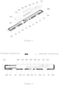
- this embodiment provides a phase shifter, including: a first circuit layer 100, the first circuit layer 100 having at least two output ports (specifically, in this embodiment, for ease of description, five output ports, namely P1 to P5 are described) and at least one input port IN (in order to simplify the first circuit layer 100, only one input port IN is provided in this embodiment), the first circuit layer 100 being provided with an input branch 130 and a first output branch 140, and the input branch 130 being electrically connected to the input port 110; a second circuit layer 200, with reference to Figures 2 to 7 , the second circuit layer 200 being able to move relative to the first circuit layer 100, referring to figures 4 and 7 , when the second circuit layer 200 moves to the first position relative to the first circuit layer 100, the first output branch 140 being disconnected from the input branch 130, with reference to figures 2 , 3 , 5 and 6 , when the second circuit layer 200 moves to the second position relative to the first circuit layer 100, the first output branch 140 and the input branch 130 being connected, specifically in this embodiment,
- the dielectric plate 300 can move relative to the first circuit layer 100.
- the dielectric plate 300 can drive the second circuit layer 200 to switch between the above-mentioned first position and the second position, thereby realizing the connection and disconnection between the first output branch 140 and the input branch 130.
- the above-mentioned first circuit layer 100 further includes a second output branch 150, and the second output branch 150 and the input branch 130 are always electrically connected.
- at least one branch in the first circuit layer 100 of the phase shifter can always be in a conductive state.
- at least one of the radiation units connected to the output ports P1 to P5 of the phase shifter may always be in the working state.
- the second circuit layer 200 is used to separately control the on/off of the two output branches and the input branch 130.
- it must also ensure that at least one output branch and input branch 130 are connected during the operation of the phase shifter. Therefore, the complexity of the entire on/off control can be simplified, which is beneficial to simplify the structure of the phase shifter.
- the first circuit layer 100 of the phase shifter may also have multiple first output branches 140 without the second output branch 150, which is not limited.
- the phase shifter may include four first output branches 140 and one second output branch 150.
- the four first output branches 140 correspond to the output ports P1, P2, P4, and P5, respectively, and the second output branch 150 corresponds to output port P3.
- the following description is made using this number as an example.
- the input branch 130 is electrically connected to an input end of the antenna signal through the input port 110.
- the output ports of the first output branch 140 (specifically the output ports P1, P2, P4, and P5 in this embodiment) and the output ports of the second output branch 150 (specifically output port P3 in this embodiment) are used for electrical connection with the corresponding radiation unit (not shown).
- the second circuit layer 200 is in the first position, the first output branch 140 is disconnected from the input branch 130, and the radiation units connected to the first output ports P1, P2, P4, and P5 are unenabled, the radiation unit connected to the output port P3 is in working condition, while the antenna can have a wider beam width.
- the first output branch 140 is connected to the input branch 130, and the radiation units connected to the output ports P1 to P5 are all in working state.
- the antenna has a narrow beam width.
- the output port of the phase shifter is connected to at least two radiation units in working state, by moving the dielectric plate 300 of the phase shifter, the overlap area between the dielectric plate 300 and the first circuit layer 100 can be changed, thereby performing adjustment of the down-tilt angle of the antenna.
- the phase shifter has the second circuit layer 200 and uses the movement of the dielectric plate 300 relative to the first circuit layer 100 to drive the second circuit layer 200 to move relative to the first circuit layer 100.
- It can control the connection/disconnection of the first output branch 140 and the input branch 130 while realizing the down-tilt angle adjustment, thereby changing the number of radiation units connected to the phase shifter in working state, and then realizing the adjustment of the antenna's beam width. Its overall structure is simple and compact, it can adapt to different coverage scenarios, and has broad application prospects.
- the first output branch 140 and the input branch 130 are insulated from each other.
- the second circuit layer 200 is provided between the first output branch 140 and the input branch 130.
- the second circuit layer 200 controls the connection/disconnection between the input branch 130 and the first output branch 140 through coupling/disconnection with the input branch 130 and the first output branch 140.
- the second circuit layer 200 can act like a coupling switch, and it is more convenient for the dielectric plate 300 to control its on/off.
- the movement of the dielectric plate 300 relative to the first circuit layer 100 includes a forward movement (in the direction shown by the solid arrow in the figures) and a reverse movement (as shown in the direction indicated by the hollow arrow of the same figures).
- the above-mentioned switching of the second circuit layer 200 from the first position to the second position is realized by the reverse movement of the dielectric plate 300.
- the above-mentioned switching of the second circuit layer 200 from the second position to the first position is realized by the forward movement of the dielectric plate 300.
- This one-way control method can further simplify the structure of the phase shifter.
- the phase shifter further includes a substrate 400, and the second circuit layer 200 is disposed on the substrate 400.
- the material of the substrate 400 can be any one or more of existing insulating materials, such as circuit plate substrates or plastics.
- the first circuit layer 100 can also be disposed on another substrate, and then fixed in the cavity of the phase shifter through the substrate, which is not described in detail here.
- the above-mentioned dielectric plate 300 may be slidably connected to the substrate provided with the first circuit layer 100, so as to more accurately control the relative position of the dielectric plate 300 and the first circuit layer 100.
- the dielectric plate 300 is provided with a first driving portion 311 for driving the second circuit layer 200 to move from a first position to a second position, and a second driving portion 312 for driving the second circuit layer 200 to move from the second position to the first position.
- the first driving portion 311 and the second driving portion 312 are spaced apart.
- the first driving portion 311 and the second driving portion 312 drive the substrate 400 to drive the second circuit layer 200 to switch between the first position and the second position.
- the substrate 400 is pushed by the first driving portion 311 to move from the first position to the second position.
- the dielectric plate 300 moves in the opposite direction of the first preset direction (that is, the above-mentioned forward movement), that is, when the state shown in Figure 3 is switched to the state shown in Figure 4 , the substrate is pushed by the second driving portion 312 400 to move from the second position to the first position.
- the movement of the dielectric plate 300 relative to the first circuit layer 100 is a linear movement.
- the dielectric plate 300 can move along a preset straight line. In this way, the area of the dielectric plate 300 corresponding to each output port 120 can be changed, thereby changing the phase difference of each output port 120 and realizing the adjustment of the antenna down-tilt angle.
- the dielectric plate 300 can continue to move in the reverse direction according to a preset straight line, thereby forming the state shown in Figure 2 .
- the second driving portion 312 will not cooperate with the substrate 400, and the second circuit layer 200 is still in the second position.
- the first output branch 140 and the four second output branches 150 of the phase shifter are all in a conducting state.
- the radiation units connected to the output ports P1 ⁇ P5 are all in working condition.
- the phase shifter can adjust the down-tilt angle of the antenna through the movement of the dielectric plate 300.
- the second driving portion 312 can push the substrate 400 and accordingly drive the second circuit layer 200 to move from the second position to the first position.
- the input branch and the four first output branches 140 are disconnected, so that the four radiation units are unenabled, and only the radiation unit connected to the port P3 works, thereby realizing the adjustment of the antenna beam width.
- first position and second position can be set according to actual needs.
- the substrate 400 is provided with a first oblique end surface 410 that is at a certain angle to the moving direction of the dielectric plate 300 and a second oblique end surface 420 opposite to the first oblique end surface 410.
- the first driving portion 311 is a third oblique end surface provided on the dielectric plate 300 and adapted to the first oblique end surface 410.
- the second driving portion 312 is a fourth oblique end surface provided on the dielectric plate 300 and adapted to the second oblique end surface 420.
- each of the above-mentioned oblique end surfaces can generate a force that pushes the substrate 400 toward one side of the movement direction of the dielectric plate 300 when moving, so that the substrate 400 and the corresponding second circuit layer 200 are able to shift between the first position and the second position along an oblique track.
- This is beneficial to avoid interference with the normal movement of the dielectric plate 300, and is easy to implement, and at the same time, it does not damage the original structure of the housing of the phase shifter.
- the first oblique end surface 410 and the second oblique end surface 420 preferably have an angle of 45° with respect to the reverse movement direction of the dielectric plate 300, or 145° with respect to the forward movement direction of the dielectric plate 300.
- the following angle is also used as an example for description. It should be understood that in actual applications, the angle of the above-mentioned oblique end surfaces can be adjusted according to the actual switching direction of the second circuit layer 200, which is not limited here.
- the dielectric plate 300 is provided with a groove 310 that can accommodate the substrate 400.
- the groove 310 includes a first inner side wall 11 and a second inner side wall 12 that are arranged oppositely.
- the third oblique end surface and the fourth oblique end surface are provided by the first inner side wall 11 and the second inner side wall 12, respectively.
- the above-mentioned groove is roughly in the shape of " ".
- the " "-shaped groove includes a first longitudinal wall, a second longitudinal wall and a third longitudinal wall 13 arranged in sequence.
- the second longitudinal wall is the above-mentioned first inner side wall 11
- the first longitudinal wall is the above-mentioned second inner side wall 12.
- the height relationship between the first longitudinal wall and the second longitudinal wall is H1>H2, and the height relationship between the first longitudinal wall and the third longitudinal wall is H1>H3, and the height between the first to third longitudinal walls The relationship is H1 > H2 ⁇ H3.
- the overall structure is simple and it is easy to manufacture.
- the height H3 of the third longitudinal wall 13 should be greater than or equal to the width of the substrate 400 on which the second circuit layer 200 is provided.
- the first longitudinal wall and the second longitudinal wall having the above-mentioned height can ensure that the substrate 400 has a sufficient moving space for switching between on and off.
- the above-mentioned " "-shaped groove 310 is sequentially provided with a first lateral wall 14, a second lateral wall 15 and a third lateral wall 16 from bottom to top.
- the " "-shaped groove 310 is defined by a first longitudinal wall, a first lateral wall 14, a second longitudinal wall, a second lateral wall 15, a third longitudinal wall 13, and a third lateral wall 16 in sequence. Further preferably, the distance between the first lateral wall 14 and the second lateral wall 15 is adapted to the width of the substrate 400, so that when the substrate 400 is located in the space of the groove 310 between the first lateral wall 14 and the second lateral wall 15 (During this time, the second circuit layer 200 is in the second position, and the four first output branches 140 are in a conductive state with the input branch 130, the radiation units corresponding to the output ports P1, P2, P4, and P5 of the first output branch 140 are in the working state), and when the dielectric plate 300 moves relative to the first circuit layer 100, the first lateral wall 14 and the second lateral wall 15 can limit the substrate 400 in the longitudinal direction. This makes the first output branch 140 and the input branch 130 in the conducting state have better stability, which is beneficial to further phase adjustment.
- the above-mentioned groove 310 may also include a first strip-shaped groove 330 and a second strip-shaped groove 340 communicating with the first strip-shaped groove 330.
- the first strip-shaped groove 330 is located on one side of a lateral direction of the second strip-shaped groove 340, and the horizontal length of the first strip-shaped groove 330 is smaller than the horizontal length of the second strip-shaped groove 340.
- the second inner side wall 12 is defined by a sidewall of the first strip-shaped groove 330 and a sidewall of the second strip-shaped groove 340 which are joined to each other.
- the second inner side wall 12 is formed by another side wall, opposite to the first inner side wall 11, of the first strip-shaped groove 330.
- the first inner side wall 11 serves as the first driving portion 311 and the second inner side wall 12 serves as the second driving portion 312, when the second circuit layer 200 is located in the first strip-shaped groove 330, the second circuit layer 200 is in the first position.
- the second circuit layer 200 is located in the second strip-shaped groove 340, the second circuit layer 200 is in the second position.
- the second circuit layer 200 may not move relative to the first circuit layer 100, so that when the first output branch 140 and the input branch 130 are in a conductive state, the phase can be further stabilized and adjusted in a wide range through the dielectric plate 300.
- the horizontal length of the first strip-shaped groove 330 is preferably ⁇ the length of the substrate 400, and the horizontal length of the second strip-shaped groove 330 is preferably more than twice the length of the substrate 400.
- the above-mentioned dielectric plate and the second circuit layer can also be matched by other guiding members.
- the first driving portion and the second driving portion may be of a convex structure.
- the direction of the driving force may be set according to the movement track of the second circuit layer 200, or the movement track of the second circuit layer 200 may be set according to the direction of the formed driving force.
- a guiding structure for guiding the movement of the second circuit layer 200 is further provided on the first circuit layer 100.
- the second circuit layer 200 can be moved between the first position and the second position through the guiding structure.
- This uses the guiding structure to guide the movement of the second circuit layer 200 to form a movement track, which facilitates obtaining the direction of the pushing force, and furthermore it can set the shape and positional relationship of the first driving portion 311 and the second driving portion 312.
- the guiding structure should be adapted to the switching movement track of the substrate 400, so as to better cooperate with the first driving portion 311 and the second driving portion 312 on the dielectric plate 300 to control the movement of the substrate 400.
- the guiding structure includes a guiding rail 160 disposed on the first circuit layer 100, and a guiding member 500 disposed on the second circuit layer 200 (specifically on the substrate 400 in this embodiment).
- the guiding member 500 is in sliding fit with the guiding rail 160.
- the guiding rail 160 is provided to make the second circuit layer 200 move on the first circuit layer 100 along a preset track.
- the guiding rail 160 can have various structures, such as guiding grooves, sliding rails, and the structure of the guiding member 500 can be adaptively adjusted according to the structure of the guiding rail 160.
- two guiding structures arranged in parallel are preferably provided, so as to further improve the stability of the substrate 400 during the switching movement.
- the guiding rail 160 is an oblique guiding groove
- the guiding member 500 is slidingly fitted with the oblique guiding groove, thus enabling the second circuit layer 200 to slide along an oblique track between the first position and the second position.
- the moving track of the second circuit layer 200 is oblique, and the moving directions of the dielectric plate 300 intersect, which facilitates the formation of an oblique pushing force by arranging the first driving portion 311 and the second driving portion 312 on the dielectric plate 300.
- the first circuit layer 100 in the phase shifter may have two layers, and the two first circuit layers 100 may be electrically connected through a metal through hole, and for example, the structure may be formed by a double-layered PCB plate or by electroplating/laser carving on a non-metallic substrate.
- the structure may be formed by a double-layered PCB plate or by electroplating/laser carving on a non-metallic substrate.
- There may also be two dielectric plates 300 correspondingly, and the double-layered PCB plate or non-metallic substrate is arranged between the two dielectric plates 300. That is to say, the two dielectric plates 300 are arranged corresponding to the two first circuit layers 100. And the movement of the two dielectric plates is synchronized and in the same direction.
- the amount of change in the overlap area between the dielectric plate 300 and the first circuit layer 100 is relatively large. This is beneficial to the overall layout of the antenna when the phase shifter is required to have a larger phase shift amount.
- the second circuit layer 200 may include an upper circuit layer 201 and a lower circuit layer 201, and the upper circuit layer 201 and the lower circuit layer 201 are fixedly connected to each other and distributed in the upper and lower sides of the first circuit layer 100 respectively.
- the assembly between the second circuit layer 200 and the first circuit layer 100 is more convenient, and it is beneficial to the second circuit layer 200 and the first circuit layer 100 to be arranged close to each other.
- the simpler thing is that the upper circuit layer 201 and the lower circuit layer 201 are connected together by the guiding member 500.
- the guiding member 500 may be of a structure such as a buckle.
- the difference from the above-mentioned embodiment is that there are at least two second circuit layers 200, and each second circuit layer 200 is arranged at intervals along the moving direction of the dielectric plate 300.
- the above-mentioned first circuit layer 100 further includes a third output branch 170, and the third output branch 170 is correspondingly provided with a second circuit layer 200.
- the third output branch 170 is disconnected from the input branch 130 or from the adjacent first output branch 140.
- the third output branch 170 is connected to the input branch 130 or to the adjacent first output branch 140.
- the dielectric plate 300 can drive the second circuit layer 200 corresponding to the third output branch 170 to switch between the third position and the fourth position. In this way, it is convenient for the dielectric plate 300 to drive each second circuit layer 200 to switch between its corresponding first position and second position, and between the third position and the fourth position in different intervals of its movement distance, thereby respectively controlling the on/off between the corresponding input branch 130 and each first output branch 140. In this case, only a plurality of grooves 310 are needed to be correspondingly opened on the dielectric plate 300, and each second circuit layer 200 can be driven to move respectively, thereby further improving the beam adjustment range of the phase shifter to adapt to more coverage scene.
- the first circuit layer 100 there are 3 second circuit layers 200.
- the first output branch 140 electrically connected to the output ports P2 and P4 is insulated from the input branch 130.
- the third output branch 170 corresponding to the output ports P1 and P5 is preferably insulated from the adjacent first output branch 140. In this way, it is easier to control the coupling/separation of the third output branch 170 and the corresponding first output branch 140.
- the first circuit layer 100 is also described below.
- the 3 forward directions as 200a, 200b, and 200c in sequence.
- the three second circuit layers 200 move along the dielectric plate 300.
- the first output branch 140 and the input branch 130 respectively connected to the ports P2 and P4 corresponding to the second circuit layer 200b are in a conductive state.
- the third output branch 170 connected to the ports P1 and P5 corresponding to the second circuit layers 200a and 200b is in a disconnected state.
- the radiation units connected to the output ports P2, P3, and P4 are in working condition.
- the phase shifter is connected to 3 radiation units, and the beam width value of the antenna is about 22°.
- the first output branch 140 corresponding to the second circuit layer 200b and the third output branch 170 corresponding to the second circuit layers 200a and 200c are both in a conducting state.
- the radiation units connected to the output ports P1-P5 are all in working state. That is, the phase shifter can be connected to 5 radiation units, and the beam width value of the antenna is about 13°.
- pulling the dielectric plate 300 can change the phase of each port, so that the phase of the output port has a change relationship of 2 ⁇ , ⁇ , 0, - ⁇ , -2 ⁇ , thereby adjusting the down-tilt angle of the antenna.
- the input port IN and the output port P3 are kept in a conductive state
- the first output branch 140 corresponding to the second circuit layer 200b is in a disconnected state
- the corresponding third output branch 170 is also in a disconnected state
- the input port and the output ports P1, P2, P3 and P5 are all in the disconnected state. That is, meanwhile, the phase shifter is only connected to one radiation unit, and the beam width value of the antenna is about 65°.
- the on/off of each port of the phase shifter can be controlled, and the number of antenna radiation units can be changed, thus changing the beam width of the antenna.
- first position “first position”, “second position”, “third position” and “fourth position” are only to indicate that the second circuit layer 200 has a position for switching on/off of the circuit.
- the “first position”, “second position”, “third position” and “fourth position” can be set according to actual conditions.
- the direction of movement of each second circuit layer 200 when switching in a conduction direction may also be different.
- the number of the above-mentioned second circuit layers 200 and the number of grooves 310 on the dielectric plate 300 can be set according to actual needs, and there is no specific limitation.
- the number of ports of the phase shifter is not limited to 5, and can be set to any number of ports ⁇ 2.
- the movement of the dielectric plate 300 relative to the first circuit layer 100 may also be an arc movement, that is, the phase shifter is an arc-shaped phase shifter.
- the phase shifter is an arc-shaped phase shifter.
- the present application also provides an antenna including the above-mentioned phase shifter and radiation units respectively and correspondingly connected to the output branch of the phase shifter.
- the above-mentioned antenna is based on the same concept as the above-mentioned phase shifter embodiments, and its technical effect is the same as that of the phase shifter embodiments of the present invention.
Landscapes
- Engineering & Computer Science (AREA)
- Computer Networks & Wireless Communication (AREA)
- Waveguide Switches, Polarizers, And Phase Shifters (AREA)
- Variable-Direction Aerials And Aerial Arrays (AREA)
Claims (13)
- Phasenschieber, umfassend:eine erste Schaltungsschicht (100), wobei die erste Schaltungsschicht (100) einen Eingangszweig (130) und einen ersten Ausgangszweig (130) enthält;eine zweite Schaltungsschicht (200), wobei die zweite Schaltungsschicht (200) relativ zu der ersten Schaltungsschicht (100) beweglich ist, und, falls sich die zweite Schaltungsschicht (200) in eine erste Position relativ zu der ersten Schaltungsschicht (100) bewegt, der erste Ausgangszweig (130) von dem Eingangszweig (130) getrennt ist, falls sich die zweite Schaltungsschicht (200) in eine zweite Position relativ zu der ersten Schaltungsschicht bewegt, der erste Ausgangszweig (130) mit dem Eingangszweig (130) verbunden ist; undeine dielektrische Platte (300), die so konfiguriert ist, dass sie sich relativ zu der ersten Schaltungsschicht bewegt und die zweite Schaltungsschicht (200) antreibt, um zwischen der ersten Position und der zweiten Position zu wechseln, dadurch gekennzeichnet, dassdie Bewegung der dielektrischen Platte (300) relativ zu der ersten Schaltungsschicht eine Vorwärtsbewegung und eine Rückwärtsbewegung in einer Längsrichtung umfasst; das Schalten der zweiten Schaltungsschicht (200) von der ersten Position zu der zweiten Position durch die Rückwärtsbewegung der dielektrischen Platte (300) realisiert wird, und das Schalten der zweiten Schaltungsschicht (200) von der zweiten Position zu der ersten Position durch die Vorwärtsbewegung der dielektrischen Platte (300) realisiert wird; unddie dielektrische Platte (300) mit einem ersten Antriebsabschnitt zum Antreiben der zweiten Schaltungsschicht (200) versehen ist, um sich von der zweiten Position zu der ersten Position zu bewegen, einem zweiten Antriebsabschnitt zum Antreiben der zweiten Schaltungsschicht (200), um sich von der ersten Position zu der zweiten Position zu bewegen; und der erste Antriebsabschnitt und der zweite Antriebsabschnitt voneinander beabstandet sind, wobei die Antriebsabschnitte die zweite Schaltungsschicht in einer bestimmten Winkelrichtung relativ zu der Bewegungsrichtung der dielektrischen Platte antreiben.
- Phasenschieber nach Anspruch 1, wobei der erste Ausgangszweig (130) von dem Eingangszweig (130) isoliert ist, die zweite Schaltungsschicht (200) zwischen dem ersten Ausgangszweig (130) und dem Eingangszweig (130) vorgesehen ist; und die zweite Schaltungsschicht (200) die Verbindung/Trennung des Eingangszweigs (130) und des ersten Ausgangszweigs (130) durch Kopplung/Trennung mit dem Eingangszweig (130) bzw. dem ersten Ausgangszweig (130) steuert.
- Phasenschieber nach Anspruch 1, wobei die erste Schaltungsschicht ferner einen zweiten Ausgangszweig aufweist und der zweite Ausgangszweig elektrisch mit dem Eingangszweig (130) verbunden ist.
- Phasenschieber nach Anspruch 3, wobei die zweite Schaltungsschicht (200) auf einem Substrat (400) angeordnet ist und der erste Antriebsaschnitt und der zweite Antriebsabschnitt das Substrat (400) antreiben, so dass die zweite Schaltungsschicht (200) zwischen der ersten Position und der zweiten Position wechselt; das Substrat (400) mit einer ersten schrägen Endfläche, die in einem bestimmten Winkel zur Bewegungsrichtung der dielektrischen Platte (300) steht, und einer zweiten schrägen Endfläche gegenüber der ersten schrägen Endfläche versehen ist; der erste Antriebsabschnitt eine dritte schräge Endfläche ist, die auf der dielektrischen Platte (300) vorgesehen und an die erste schräge Endfläche angepasst ist, und der zweite Antriebssabschnitt eine vierte schräge Endfläche ist, die auf der dielektrischen Platte (300) vorgesehen und an die zweite schräge Endfläche angepasst ist.
- Phasenschieber nach Anspruch 4, wobei die dielektrische Platte (300) mit einer Nut versehen ist, die in der Lage ist, das Substrat (400) aufzunehmen; die Nut eine erste innere Seitenwand und eine zweite innere Seitenwand, die gegenüberliegend angeordnet sind, umfasst, und die erste innere Seitenwand und die zweite innere Seitenwand der dritten schrägen Endfläche und der vierten schrägen Endfläche entsprechen.
- Phasenschieber nach Anspruch 5, wobei die Nut im Wesentlichen ""-förmig ist und die "
 "-förmige Nut erste bis dritte Längswände aufweist, die in Folge angeordnet sind; und die erste Längswand und die zweite Längswand der ersten inneren Seitenwand und der zweiten inneren Seitenwand entsprechen.
 - Phasenschieber nach Anspruch 6, wobei der Abstand zwischen einer ersten und einer zweiten Seitenwand, die von unten nach oben in der ""-förmigen Nut angeordnet sind, an die Breite des Substrats (400) angepasst ist.
- Phasenschieber nach Anspruch 1, wobei die erste Schaltungsschicht (100) ferner mit einer Führungsstruktur zum Führen der Bewegung der zweiten Schaltungsschicht (200) versehen ist.
- Phasenschieber nach Anspruch 8, wobei die Führungsstruktur eine auf der ersten Schaltungsschicht (100) vorgesehene Führungsschiene (160) und ein auf der zweiten Schaltungsschicht (200) vorgesehenes Führungselement (500) umfasst und das Führungselement (500) gleitend mit der Führungsschiene (160) verbunden ist.
- Phasenschieber nach Anspruch 1, wobei die zweite Schaltungsschicht (200) eine obere Schaltungsschicht (201) und eine untere Schaltungsschicht aufweist, die relativ zueinander auf einer Ober- und Unterseite der ersten Schaltungsschicht (100) verteilt sind, und die obere Schaltungsschicht (201) und die untere Schaltungsschicht fest verbunden sind.
- Phasenschieber nach Anspruch 1, wobei zwei erste Schaltungsschichten (100) und zwei dielektrische Platten (300) vorhanden sind und die beiden ersten Schaltungsschichten (100) einander gegenüberliegend angeordnet sind und eine elektrische Verbindung aufrechterhalten; die beiden zweiten Schaltungsschichten (200) beide zwischen den beiden dielektrischen Platten (300) angeordnet sin, und die beiden dielektrischen Platten sich synchron bewegen.
- Phasenschieber nach einem der Ansprüche 1-11, wobei die erste Schaltungsschicht (100) ferner einen dritten Ausgangszweig (170) aufweist und mindestens zwei zweite Schaltungsschichten (200) vorhanden sind;diese zweiten Schaltungsschichten (200) in Abständen entlang der Bewegungsrichtung der dielektrischen Platte (300) angeordnet sind und mindestens eine der zweiten Schaltungsschichten (200) entsprechend dem dritten Ausgangszweig (170) angeordnet ist;für den Fall, dass sich die zweite Schaltungsschicht (200) in eine dritte Position relativ zur ersten Schaltungsschicht (100) bewegt, der dritte Ausgangszweig (170) von dem Eingangszweig (130) oder dem benachbarten ersten Ausgangszweig (130) getrennt wird;für den Fall, dass sich die zweite Schaltungsschicht (200) in eine vierte Position relativ zu der ersten Schaltungsschicht (100) bewegt, der dritte Ausgangszweig (170) mit dem Eingangszweig (130) oder dem benachbarten ersten Ausgangszweig (130) verbunden wird; unddie dielektrische Platte (300) die zweite Schaltungsschicht (200), die dem dritten Ausgangszweig (170) entspricht, antreiben kann, um zwischen der dritten Position und der vierten Position zu wechseln.
- Antenne, dadurch gekennzeichnet, dass sie umfasst: den Phasenschieber nach einem der Ansprüche 1 bis 12 und eine Vielzahl von Strahlungseinheiten, die jeweils mit den Ausgangsports des Phasenschiebers verbunden sind.
Applications Claiming Priority (2)
| Application Number | Priority Date | Filing Date | Title |
|---|---|---|---|
| CN201811329790.2A CN111180892B (zh) | 2018-11-09 | 2018-11-09 | 天线及移相器 |
| PCT/CN2019/090786 WO2020093696A1 (zh) | 2018-11-09 | 2019-06-11 | 天线及移相器 |
Publications (3)
| Publication Number | Publication Date |
|---|---|
| EP3879628A1 EP3879628A1 (de) | 2021-09-15 |
| EP3879628A4 EP3879628A4 (de) | 2022-01-05 |
| EP3879628B1 true EP3879628B1 (de) | 2023-04-12 |
Family
ID=70611120
Family Applications (1)
| Application Number | Title | Priority Date | Filing Date |
|---|---|---|---|
| EP19883047.3A Active EP3879628B1 (de) | 2018-11-09 | 2019-06-11 | Antenne und phasenschieber |
Country Status (3)
| Country | Link |
|---|---|
| EP (1) | EP3879628B1 (de) |
| CN (1) | CN111180892B (de) |
| WO (1) | WO2020093696A1 (de) |
Families Citing this family (11)
| Publication number | Priority date | Publication date | Assignee | Title |
|---|---|---|---|---|
| CN111600099B (zh) * | 2019-02-20 | 2021-10-26 | 华为技术有限公司 | 移相器及电调天线 |
| CN113013625B (zh) | 2019-12-20 | 2022-11-04 | 华为机器有限公司 | 一种波束调整组件及天线系统 |
| CN111585024B (zh) * | 2020-05-20 | 2023-03-31 | 中信科移动通信技术股份有限公司 | 介质移相器及5g基站天线 |
| CN111834708B (zh) * | 2020-08-31 | 2025-02-07 | 京信通信技术(广州)有限公司 | 基站天线、校准网络装置及移相器 |
| WO2022156385A1 (en) * | 2021-01-19 | 2022-07-28 | Telefonaktiebolaget Lm Ericsson (Publ) | Device for power dividing and phase shifting |
| CN112928454B (zh) * | 2021-02-01 | 2023-01-20 | 中信科移动通信技术股份有限公司 | 一种馈电网络切换装置及天线 |
| CN116315679B (zh) * | 2021-12-20 | 2025-10-14 | 苏州硕贝德创新技术研究有限公司 | 应用于Massive-MIMO天线的远程电调装置 |
| CN114758916A (zh) * | 2022-03-31 | 2022-07-15 | 昆山恩电开通信设备有限公司 | 一种射频信号开关装置 |
| EP4609468A1 (de) | 2022-10-25 | 2025-09-03 | Telefonaktiebolaget LM Ericsson (publ) | Antenne |
| CN119726120A (zh) * | 2023-09-28 | 2025-03-28 | 华为技术有限公司 | 信号调整组件、天线及通信设备 |
| CN120073322B (zh) * | 2025-04-11 | 2025-08-22 | 中兴通讯股份有限公司 | 波束调整装置及天线系统 |
Family Cites Families (18)
| Publication number | Priority date | Publication date | Assignee | Title |
|---|---|---|---|---|
| US2773242A (en) * | 1952-04-02 | 1956-12-04 | Itt | Microwave switching arrangements |
| US2990523A (en) * | 1958-12-03 | 1961-06-27 | Thompson Ramo Wooldridge Inc | Tri-plate line switch and power splitter |
| JPH104305A (ja) * | 1996-06-18 | 1998-01-06 | Furukawa Electric Co Ltd:The | 電力分配型移相器 |
| US6333683B1 (en) * | 1998-09-04 | 2001-12-25 | Agere System Optoelectronics Guardian Corp. | Reflection mode phase shifter |
| CA2298326A1 (en) * | 1999-03-02 | 2000-09-02 | Li-Chung Chang | Ultrawide bandwidth electromechanical phase shifter |
| JP3310260B2 (ja) * | 2000-07-19 | 2002-08-05 | 日本電業工作株式会社 | 移相器 |
| JP2005303690A (ja) * | 2004-04-13 | 2005-10-27 | Makita Corp | 移相器 |
| KR101567882B1 (ko) * | 2009-05-11 | 2015-11-12 | 주식회사 케이엠더블유 | 수직 빔틸트 제어 안테나를 위한 다중 이상기 |
| US20110140805A1 (en) * | 2009-12-16 | 2011-06-16 | Wha Yu Industrial Co., Ltd. | Phase shifter |
| KR101089514B1 (ko) * | 2010-01-21 | 2011-12-05 | (주)하이게인안테나 | 이동통신 안테나용 전력위상가변기 |
| CN101820090A (zh) * | 2010-04-15 | 2010-09-01 | 中国科学技术大学 | 一种采用齿状或梳状结构介质滑片的新型移相器 |
| CN203787537U (zh) * | 2014-03-27 | 2014-08-20 | 华为技术有限公司 | 一种电调天线移相器 |
| CN104090531B (zh) * | 2014-06-06 | 2017-01-04 | 西安华为技术有限公司 | 开关组件、开关组件控制方法、控制器及基站 |
| CN106921011B (zh) * | 2015-12-28 | 2019-07-19 | 西安华为技术有限公司 | 一种移相器及天线 |
| WO2018120618A1 (zh) * | 2016-12-27 | 2018-07-05 | 深圳国人通信股份有限公司 | 一种小型化单步式移相器 |
| CN106684561B (zh) * | 2017-01-16 | 2023-07-07 | 东南大学 | 一种天线结构及设计方法 |
| CN108598707B (zh) * | 2018-05-29 | 2024-03-22 | 深圳国人无线通信有限公司 | 一种移相器开关 |
| CN109638391B (zh) * | 2018-11-09 | 2020-07-07 | 华南理工大学 | 介质移动式移相器及基站天线 |
-
2018
- 2018-11-09 CN CN201811329790.2A patent/CN111180892B/zh active Active
-
2019
- 2019-06-11 WO PCT/CN2019/090786 patent/WO2020093696A1/zh not_active Ceased
- 2019-06-11 EP EP19883047.3A patent/EP3879628B1/de active Active
Also Published As
| Publication number | Publication date |
|---|---|
| CN111180892A (zh) | 2020-05-19 |
| EP3879628A1 (de) | 2021-09-15 |
| WO2020093696A1 (zh) | 2020-05-14 |
| CN111180892B (zh) | 2021-05-07 |
| EP3879628A4 (de) | 2022-01-05 |
Similar Documents
| Publication | Publication Date | Title |
|---|---|---|
| EP3879628A1 (de) | Antenne und phasenschieber | |
| EP2879235B1 (de) | Modul für phasenverschiebungseinheit, herstellungsverfahren dafür, phasenverschiebungsvorrichtung und antenne | |
| CN109921157B (zh) | 移相器及天线 | |
| EP3823089B1 (de) | Phasenumschalter und elektrische schwenkantenne | |
| CN103094689B (zh) | 介质移相模块及其移相单元、馈电网络和天线 | |
| US11552396B2 (en) | Phase shifter, remote electrical tilt system and base station antenna | |
| CN106972267B (zh) | 一种应用于基站天线的空间立体移相器 | |
| US11955720B2 (en) | Beam adjustment assembly and antenna system | |
| AU2022321036B2 (en) | Phase shifter with adjustable output mode and antenna | |
| Ruiz-Cruz et al. | Waveguide antenna feeders with integrated reconfigurable dual circular polarization | |
| CN104103875A (zh) | 移相器及包含移相器的移相组件、移相馈电网络 | |
| CN105140600B (zh) | 小型化介质移相器组及天线阵馈电网络 | |
| CN209607890U (zh) | 移相器及天线 | |
| CN103956577A (zh) | 一种4g天线的一体化馈电网络 | |
| CN109994804B (zh) | 移相器及天线 | |
| CN201838690U (zh) | 具有反向相对配置型态电调单元的移相器 | |
| CN209329114U (zh) | 移相器及天线 | |
| CN204011610U (zh) | 移相器及包含移相器的移相组件、移相馈电网络 | |
| CN117728184A (zh) | 一种新型的移相器网络装置及天线 | |
| CN110137635B (zh) | 一种移相器介质结构、移相器及基站天线 | |
| CN113193313B (zh) | 移相器及天线系统 | |
| CN201369377Y (zh) | 一种基于介质加载的移相器模块 | |
| CN203326112U (zh) | 可连续变相的馈电网络 | |
| CN215600517U (zh) | 移相器及天线系统 | |
| CN210956929U (zh) | 天线及移相器 |
Legal Events
| Date | Code | Title | Description |
|---|---|---|---|
| STAA | Information on the status of an ep patent application or granted ep patent |
Free format text: STATUS: THE INTERNATIONAL PUBLICATION HAS BEEN MADE |
|
| PUAI | Public reference made under article 153(3) epc to a published international application that has entered the european phase |
Free format text: ORIGINAL CODE: 0009012 |
|
| STAA | Information on the status of an ep patent application or granted ep patent |
Free format text: STATUS: REQUEST FOR EXAMINATION WAS MADE |
|
| 17P | Request for examination filed |
Effective date: 20210602 |
|
| AK | Designated contracting states |
Kind code of ref document: A1 Designated state(s): AL AT BE BG CH CY CZ DE DK EE ES FI FR GB GR HR HU IE IS IT LI LT LU LV MC MK MT NL NO PL PT RO RS SE SI SK SM TR |
|
| REG | Reference to a national code |
Ref country code: DE Ref legal event code: R079 Ref document number: 602019027569 Country of ref document: DE Free format text: PREVIOUS MAIN CLASS: H01Q0003300000 Ipc: H01Q0003320000 |
|
| A4 | Supplementary search report drawn up and despatched |
Effective date: 20211208 |
|
| RIC1 | Information provided on ipc code assigned before grant |
Ipc: H01Q 1/24 20060101ALI20211202BHEP Ipc: H01Q 3/24 20060101ALI20211202BHEP Ipc: H01P 1/18 20060101ALI20211202BHEP Ipc: H01Q 3/32 20060101AFI20211202BHEP |
|
| DAV | Request for validation of the european patent (deleted) | ||
| DAX | Request for extension of the european patent (deleted) | ||
| GRAP | Despatch of communication of intention to grant a patent |
Free format text: ORIGINAL CODE: EPIDOSNIGR1 |
|
| STAA | Information on the status of an ep patent application or granted ep patent |
Free format text: STATUS: GRANT OF PATENT IS INTENDED |
|
| INTG | Intention to grant announced |
Effective date: 20221123 |
|
| GRAS | Grant fee paid |
Free format text: ORIGINAL CODE: EPIDOSNIGR3 |
|
| GRAA | (expected) grant |
Free format text: ORIGINAL CODE: 0009210 |
|
| STAA | Information on the status of an ep patent application or granted ep patent |
Free format text: STATUS: THE PATENT HAS BEEN GRANTED |
|
| AK | Designated contracting states |
Kind code of ref document: B1 Designated state(s): AL AT BE BG CH CY CZ DE DK EE ES FI FR GB GR HR HU IE IS IT LI LT LU LV MC MK MT NL NO PL PT RO RS SE SI SK SM TR |
|
| REG | Reference to a national code |
Ref country code: GB Ref legal event code: FG4D |
|
| REG | Reference to a national code |
Ref country code: CH Ref legal event code: EP |
|
| REG | Reference to a national code |
Ref country code: DE Ref legal event code: R096 Ref document number: 602019027569 Country of ref document: DE |
|
| REG | Reference to a national code |
Ref country code: IE Ref legal event code: FG4D |
|
| REG | Reference to a national code |
Ref country code: AT Ref legal event code: REF Ref document number: 1560312 Country of ref document: AT Kind code of ref document: T Effective date: 20230515 |
|
| REG | Reference to a national code |
Ref country code: SE Ref legal event code: TRGR |
|
| REG | Reference to a national code |
Ref country code: LT Ref legal event code: MG9D |
|
| REG | Reference to a national code |
Ref country code: NL Ref legal event code: MP Effective date: 20230412 |
|
| P01 | Opt-out of the competence of the unified patent court (upc) registered |
Effective date: 20230727 |
|
| REG | Reference to a national code |
Ref country code: AT Ref legal event code: MK05 Ref document number: 1560312 Country of ref document: AT Kind code of ref document: T Effective date: 20230412 |
|
| PG25 | Lapsed in a contracting state [announced via postgrant information from national office to epo] |
Ref country code: NL Free format text: LAPSE BECAUSE OF FAILURE TO SUBMIT A TRANSLATION OF THE DESCRIPTION OR TO PAY THE FEE WITHIN THE PRESCRIBED TIME-LIMIT Effective date: 20230412 |
|
| PG25 | Lapsed in a contracting state [announced via postgrant information from national office to epo] |
Ref country code: PT Free format text: LAPSE BECAUSE OF FAILURE TO SUBMIT A TRANSLATION OF THE DESCRIPTION OR TO PAY THE FEE WITHIN THE PRESCRIBED TIME-LIMIT Effective date: 20230814 Ref country code: NO Free format text: LAPSE BECAUSE OF FAILURE TO SUBMIT A TRANSLATION OF THE DESCRIPTION OR TO PAY THE FEE WITHIN THE PRESCRIBED TIME-LIMIT Effective date: 20230712 Ref country code: ES Free format text: LAPSE BECAUSE OF FAILURE TO SUBMIT A TRANSLATION OF THE DESCRIPTION OR TO PAY THE FEE WITHIN THE PRESCRIBED TIME-LIMIT Effective date: 20230412 Ref country code: AT Free format text: LAPSE BECAUSE OF FAILURE TO SUBMIT A TRANSLATION OF THE DESCRIPTION OR TO PAY THE FEE WITHIN THE PRESCRIBED TIME-LIMIT Effective date: 20230412 |
|
| PG25 | Lapsed in a contracting state [announced via postgrant information from national office to epo] |
Ref country code: RS Free format text: LAPSE BECAUSE OF FAILURE TO SUBMIT A TRANSLATION OF THE DESCRIPTION OR TO PAY THE FEE WITHIN THE PRESCRIBED TIME-LIMIT Effective date: 20230412 Ref country code: PL Free format text: LAPSE BECAUSE OF FAILURE TO SUBMIT A TRANSLATION OF THE DESCRIPTION OR TO PAY THE FEE WITHIN THE PRESCRIBED TIME-LIMIT Effective date: 20230412 Ref country code: LV Free format text: LAPSE BECAUSE OF FAILURE TO SUBMIT A TRANSLATION OF THE DESCRIPTION OR TO PAY THE FEE WITHIN THE PRESCRIBED TIME-LIMIT Effective date: 20230412 Ref country code: LT Free format text: LAPSE BECAUSE OF FAILURE TO SUBMIT A TRANSLATION OF THE DESCRIPTION OR TO PAY THE FEE WITHIN THE PRESCRIBED TIME-LIMIT Effective date: 20230412 Ref country code: IS Free format text: LAPSE BECAUSE OF FAILURE TO SUBMIT A TRANSLATION OF THE DESCRIPTION OR TO PAY THE FEE WITHIN THE PRESCRIBED TIME-LIMIT Effective date: 20230812 Ref country code: HR Free format text: LAPSE BECAUSE OF FAILURE TO SUBMIT A TRANSLATION OF THE DESCRIPTION OR TO PAY THE FEE WITHIN THE PRESCRIBED TIME-LIMIT Effective date: 20230412 Ref country code: GR Free format text: LAPSE BECAUSE OF FAILURE TO SUBMIT A TRANSLATION OF THE DESCRIPTION OR TO PAY THE FEE WITHIN THE PRESCRIBED TIME-LIMIT Effective date: 20230713 Ref country code: AL Free format text: LAPSE BECAUSE OF FAILURE TO SUBMIT A TRANSLATION OF THE DESCRIPTION OR TO PAY THE FEE WITHIN THE PRESCRIBED TIME-LIMIT Effective date: 20230412 |
|
| PG25 | Lapsed in a contracting state [announced via postgrant information from national office to epo] |
Ref country code: FI Free format text: LAPSE BECAUSE OF FAILURE TO SUBMIT A TRANSLATION OF THE DESCRIPTION OR TO PAY THE FEE WITHIN THE PRESCRIBED TIME-LIMIT Effective date: 20230412 |
|
| REG | Reference to a national code |
Ref country code: DE Ref legal event code: R119 Ref document number: 602019027569 Country of ref document: DE |
|
| PG25 | Lapsed in a contracting state [announced via postgrant information from national office to epo] |
Ref country code: SK Free format text: LAPSE BECAUSE OF FAILURE TO SUBMIT A TRANSLATION OF THE DESCRIPTION OR TO PAY THE FEE WITHIN THE PRESCRIBED TIME-LIMIT Effective date: 20230412 |
|
| PG25 | Lapsed in a contracting state [announced via postgrant information from national office to epo] |
Ref country code: MC Free format text: LAPSE BECAUSE OF FAILURE TO SUBMIT A TRANSLATION OF THE DESCRIPTION OR TO PAY THE FEE WITHIN THE PRESCRIBED TIME-LIMIT Effective date: 20230412 |
|
| PG25 | Lapsed in a contracting state [announced via postgrant information from national office to epo] |
Ref country code: SM Free format text: LAPSE BECAUSE OF FAILURE TO SUBMIT A TRANSLATION OF THE DESCRIPTION OR TO PAY THE FEE WITHIN THE PRESCRIBED TIME-LIMIT Effective date: 20230412 Ref country code: SK Free format text: LAPSE BECAUSE OF FAILURE TO SUBMIT A TRANSLATION OF THE DESCRIPTION OR TO PAY THE FEE WITHIN THE PRESCRIBED TIME-LIMIT Effective date: 20230412 Ref country code: RO Free format text: LAPSE BECAUSE OF FAILURE TO SUBMIT A TRANSLATION OF THE DESCRIPTION OR TO PAY THE FEE WITHIN THE PRESCRIBED TIME-LIMIT Effective date: 20230412 Ref country code: MC Free format text: LAPSE BECAUSE OF FAILURE TO SUBMIT A TRANSLATION OF THE DESCRIPTION OR TO PAY THE FEE WITHIN THE PRESCRIBED TIME-LIMIT Effective date: 20230412 Ref country code: EE Free format text: LAPSE BECAUSE OF FAILURE TO SUBMIT A TRANSLATION OF THE DESCRIPTION OR TO PAY THE FEE WITHIN THE PRESCRIBED TIME-LIMIT Effective date: 20230412 Ref country code: DK Free format text: LAPSE BECAUSE OF FAILURE TO SUBMIT A TRANSLATION OF THE DESCRIPTION OR TO PAY THE FEE WITHIN THE PRESCRIBED TIME-LIMIT Effective date: 20230412 Ref country code: CZ Free format text: LAPSE BECAUSE OF FAILURE TO SUBMIT A TRANSLATION OF THE DESCRIPTION OR TO PAY THE FEE WITHIN THE PRESCRIBED TIME-LIMIT Effective date: 20230412 |
|
| REG | Reference to a national code |
Ref country code: CH Ref legal event code: PL |
|
| PLBE | No opposition filed within time limit |
Free format text: ORIGINAL CODE: 0009261 |
|
| STAA | Information on the status of an ep patent application or granted ep patent |
Free format text: STATUS: NO OPPOSITION FILED WITHIN TIME LIMIT |
|
| REG | Reference to a national code |
Ref country code: BE Ref legal event code: MM Effective date: 20230630 |
|
| PG25 | Lapsed in a contracting state [announced via postgrant information from national office to epo] |
Ref country code: LU Free format text: LAPSE BECAUSE OF NON-PAYMENT OF DUE FEES Effective date: 20230611 |
|
| 26N | No opposition filed |
Effective date: 20240115 |
|
| GBPC | Gb: european patent ceased through non-payment of renewal fee |
Effective date: 20230712 |
|
| REG | Reference to a national code |
Ref country code: IE Ref legal event code: MM4A |
|
| PG25 | Lapsed in a contracting state [announced via postgrant information from national office to epo] |
Ref country code: LU Free format text: LAPSE BECAUSE OF NON-PAYMENT OF DUE FEES Effective date: 20230611 |
|
| PG25 | Lapsed in a contracting state [announced via postgrant information from national office to epo] |
Ref country code: IE Free format text: LAPSE BECAUSE OF NON-PAYMENT OF DUE FEES Effective date: 20230611 |
|
| PG25 | Lapsed in a contracting state [announced via postgrant information from national office to epo] |
Ref country code: IE Free format text: LAPSE BECAUSE OF NON-PAYMENT OF DUE FEES Effective date: 20230611 Ref country code: DE Free format text: LAPSE BECAUSE OF NON-PAYMENT OF DUE FEES Effective date: 20240103 Ref country code: GB Free format text: LAPSE BECAUSE OF NON-PAYMENT OF DUE FEES Effective date: 20230712 Ref country code: CH Free format text: LAPSE BECAUSE OF NON-PAYMENT OF DUE FEES Effective date: 20230630 |
|
| PG25 | Lapsed in a contracting state [announced via postgrant information from national office to epo] |
Ref country code: SI Free format text: LAPSE BECAUSE OF FAILURE TO SUBMIT A TRANSLATION OF THE DESCRIPTION OR TO PAY THE FEE WITHIN THE PRESCRIBED TIME-LIMIT Effective date: 20230412 |
|
| PG25 | Lapsed in a contracting state [announced via postgrant information from national office to epo] |
Ref country code: SI Free format text: LAPSE BECAUSE OF FAILURE TO SUBMIT A TRANSLATION OF THE DESCRIPTION OR TO PAY THE FEE WITHIN THE PRESCRIBED TIME-LIMIT Effective date: 20230412 Ref country code: IT Free format text: LAPSE BECAUSE OF FAILURE TO SUBMIT A TRANSLATION OF THE DESCRIPTION OR TO PAY THE FEE WITHIN THE PRESCRIBED TIME-LIMIT Effective date: 20230412 Ref country code: FR Free format text: LAPSE BECAUSE OF NON-PAYMENT OF DUE FEES Effective date: 20230612 Ref country code: BE Free format text: LAPSE BECAUSE OF NON-PAYMENT OF DUE FEES Effective date: 20230630 |
|
| PG25 | Lapsed in a contracting state [announced via postgrant information from national office to epo] |
Ref country code: BG Free format text: LAPSE BECAUSE OF FAILURE TO SUBMIT A TRANSLATION OF THE DESCRIPTION OR TO PAY THE FEE WITHIN THE PRESCRIBED TIME-LIMIT Effective date: 20230412 |
|
| PG25 | Lapsed in a contracting state [announced via postgrant information from national office to epo] |
Ref country code: BG Free format text: LAPSE BECAUSE OF FAILURE TO SUBMIT A TRANSLATION OF THE DESCRIPTION OR TO PAY THE FEE WITHIN THE PRESCRIBED TIME-LIMIT Effective date: 20230412 |
|
| PG25 | Lapsed in a contracting state [announced via postgrant information from national office to epo] |
Ref country code: CY Free format text: LAPSE BECAUSE OF FAILURE TO SUBMIT A TRANSLATION OF THE DESCRIPTION OR TO PAY THE FEE WITHIN THE PRESCRIBED TIME-LIMIT; INVALID AB INITIO Effective date: 20190611 |
|
| PGFP | Annual fee paid to national office [announced via postgrant information from national office to epo] |
Ref country code: SE Payment date: 20250618 Year of fee payment: 7 |
|
| PG25 | Lapsed in a contracting state [announced via postgrant information from national office to epo] |
Ref country code: HU Free format text: LAPSE BECAUSE OF FAILURE TO SUBMIT A TRANSLATION OF THE DESCRIPTION OR TO PAY THE FEE WITHIN THE PRESCRIBED TIME-LIMIT; INVALID AB INITIO Effective date: 20190611 |
|
| PG25 | Lapsed in a contracting state [announced via postgrant information from national office to epo] |
Ref country code: TR Free format text: LAPSE BECAUSE OF FAILURE TO SUBMIT A TRANSLATION OF THE DESCRIPTION OR TO PAY THE FEE WITHIN THE PRESCRIBED TIME-LIMIT Effective date: 20230412 |