EP3874919B1 - Gehäuse für einen switch für bahnanwendungen - Google Patents
Gehäuse für einen switch für bahnanwendungen Download PDFInfo
- Publication number
- EP3874919B1 EP3874919B1 EP19801241.1A EP19801241A EP3874919B1 EP 3874919 B1 EP3874919 B1 EP 3874919B1 EP 19801241 A EP19801241 A EP 19801241A EP 3874919 B1 EP3874919 B1 EP 3874919B1
- Authority
- EP
- European Patent Office
- Prior art keywords
- housing
- circuit board
- switch
- separating element
- outputs
- Prior art date
- Legal status (The legal status is an assumption and is not a legal conclusion. Google has not performed a legal analysis and makes no representation as to the accuracy of the status listed.)
- Active
Links
Images




Classifications
-
- H—ELECTRICITY
- H05—ELECTRIC TECHNIQUES NOT OTHERWISE PROVIDED FOR
- H05K—PRINTED CIRCUITS; CASINGS OR CONSTRUCTIONAL DETAILS OF ELECTRIC APPARATUS; MANUFACTURE OF ASSEMBLAGES OF ELECTRICAL COMPONENTS
- H05K5/00—Casings, cabinets or drawers for electric apparatus
- H05K5/06—Hermetically-sealed casings
- H05K5/069—Other details of the casing, e.g. wall structure, passage for a connector, a cable, a shaft
-
- B—PERFORMING OPERATIONS; TRANSPORTING
- B61—RAILWAYS
- B61L—GUIDING RAILWAY TRAFFIC; ENSURING THE SAFETY OF RAILWAY TRAFFIC
- B61L15/00—Indicators provided on the vehicle or train for signalling purposes
- B61L15/0018—Communication with or on the vehicle or train
- B61L15/0036—Conductor-based, e.g. using CAN-Bus, train-line or optical fibres
-
- H—ELECTRICITY
- H05—ELECTRIC TECHNIQUES NOT OTHERWISE PROVIDED FOR
- H05K—PRINTED CIRCUITS; CASINGS OR CONSTRUCTIONAL DETAILS OF ELECTRIC APPARATUS; MANUFACTURE OF ASSEMBLAGES OF ELECTRICAL COMPONENTS
- H05K5/00—Casings, cabinets or drawers for electric apparatus
- H05K5/02—Details
- H05K5/0247—Electrical details of casings, e.g. terminals, passages for cables or wiring
-
- H—ELECTRICITY
- H05—ELECTRIC TECHNIQUES NOT OTHERWISE PROVIDED FOR
- H05K—PRINTED CIRCUITS; CASINGS OR CONSTRUCTIONAL DETAILS OF ELECTRIC APPARATUS; MANUFACTURE OF ASSEMBLAGES OF ELECTRICAL COMPONENTS
- H05K5/00—Casings, cabinets or drawers for electric apparatus
- H05K5/02—Details
- H05K5/03—Covers
Definitions
- the invention relates to a housing for a switch for railway applications according to the features of the preamble of patent claim 1.
- Switches that have a housing and are installed in particular in railway passenger carriages are well known. These are used for data transmission and, if necessary, also for energy transmission.
- a generic housing is from the EN 10 2010 062 837 B3 known.
- the invention is therefore based on the object of improving a switch for railway applications compared to known switches, in particular with regard to a compact design and improved control operation.
- the housing of the switch has a flat part and, starting from this flat part, a higher part protrudes above it, with the inputs and outputs of the flat part being arranged on the top of this part and the cables with their connectors being plugged into these inputs and outputs approximately vertically.
- the other inputs and outputs in the higher part are arranged approximately at right angles to this.
- the housing of the new switch has an approximately L-shaped cross-section in section or when viewed from the side, with the inputs and outputs on one side protruding approximately vertically upwards and the inputs and outputs extending approximately at right angles to this from the other side.
- Another advantage of this connector arrangement is that all connections are in just one area, but are still fairly easy to reach. This means that the remaining area is free of cables and cooling fins can function more effectively because natural convection is less obstructed. Components with increased power dissipation can then be placed in this area.
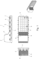
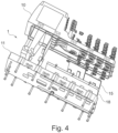
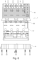
- Figures 3 to 7 three-dimensional views of the switch in various exploded views.
- FIG. 1 shows, as far as shown in detail, various views of a switch 1 for railway applications.
- This switch 1 has a housing 2, the housing 2 having a bottom 3 with which the housing 2 is placed, for example, on a surface of an installation location of the switch 1 and, if necessary, fastened.
- a first leg 4 (flat) of the housing 2 Approximately parallel to the bottom 3 there is a first leg 4 (flat) of the housing 2, with a further leg 5 (also flat) arranged approximately perpendicular to this first leg 4.
- the transition area between the two legs 4, 5 can be sharp-edged, for example at an angle of 90°. In the exemplary embodiment shown, the transition area is rounded.
- On the top of the leg 4 there is at least one connection, but preferably several connections for plug connectors or the like.
- connection are at least one input 6, preferably several inputs, and/or at least one output 7, preferably several outputs 7.
- at least one output and/or one input is present on the surface of the leg 5.
- the number of inputs 6, 8 and outputs 7, 9 shown is exemplary and can be larger or smaller depending on the application.
- the switch 1 has a housing, wherein the switch 1 is suitable and designed for railway applications and the housing 2 has an approximately L-shaped cross-section in section or viewed from the side, wherein the inputs 6 and outputs 7 on the one leg 4 protrude approximately vertically upwards and the inputs 8 and outputs 9 extend approximately at a parallel angle thereto from the other leg 5.
- FIG 2 is a plan view of the switch 1 from above.
- the housing 2 is at least divided into two parts.
- the housing 2 has an upper part 10 and a lower part 11.
- the lower part 11 is flat, with the upper part 10 having the two flat areas that form the legs 4 and 5.
- the upwardly projecting end of the leg 5 is followed by a roof-shaped design of the upper part 10.
- the upper part 10 and/or the lower part 11 have cooling fins 13 at the end, in particular in the area of the roof-shaped design of the upper part 10.
- Such cooling fins can also be provided in the transition area, in particular an arcuate transition area, from the leg 4 in the direction of the leg 5.
- At least one circuit board is arranged within the housing 2, with electrical, electromechanical and electronic components arranged on the circuit board for implementing the function of the switch 1.
- the at least one circuit board is connected to the inputs and outputs accordingly, so that signals from outside can be fed to the components via the inputs, processed there and output again via the outputs.
- two circuit boards 14, 15 are arranged separately from one another in the area of the leg 4, more precisely below the surface of this leg 4.
- the two circuit boards 14, 15 are arranged approximately parallel to the underside 3 in the housing 2.
- a further circuit board 16 which is arranged parallel below the two circuit boards 14, 15.
- a circuit board 17 is provided approximately perpendicularly, preferably exactly perpendicularly to the circuit boards 14, 15, 16 in the area of the further leg 5.
- more than one circuit board 17 can be arranged.
- a separating element 18 is provided within the housing 2.
- a thermal coupling of the circuit boards can also be implemented for increased heat distribution or heat dissipation of the electronic components.
- the Separating element does not have a thermally separating but a thermally connecting (transferring) property.
- the term "separating element" is used generally or in connection with the description of the embodiment for the separating or thermally coupling property.
- the separating element 18 is designed to be flat. It can be made of electrically conductive material, such as a steel sheet, but also of non-electrically conductive material, such as a plastic. For thermal separation of the two circuit boards 14, 15 from the circuit board 16, the separating element 18 can be made of an insulating material, for example a plastic, and extends over the entire surface of the underside 3 of the housing 2. If an electrical and/or mechanical separation of the two circuit boards 14, 15 (or only one circuit board or more than 2 circuit boards) from the circuit board 17 is intended, the separating element 18 is made of an electrically conductive material. This allows the components on the circuit boards 14, 15 in particular to be shielded from interference from the components on the circuit board 16 (or vice versa).
- the separating element 18 is attached to the housing 2 with at least one screw 19, preferably several screws, for example as in Figure 3 shown attached to the lower part 11 of the housing 2.
- the separating element 18 has at least one recess 20, preferably several recesses 20.
- a plug connector 21 which is arranged on the circuit board 16, can be passed through the separating element 18 and connected to a corresponding mating plug connector on the circuit board 14 or 15.
- a seal 22 can be inserted between the circumferential free edges of the upper part 10 and the lower part 11.
- circuit boards and, if applicable, the separating element, which are arranged in the region of the leg 4 also apply analogously to the at least one circuit board and, if applicable, a further separating element in the region of the leg 5.
- the assembly process can also be taken.
- the lower part 11 is provided, the circuit board 16 is inserted there and then the separating element 18 is mounted.
- the at least one circuit board 14, as shown the two circuit boards 14,15 is arranged on the separating element 18 and fastened in a suitable manner.
- the upper part 10 of the housing 2 is placed on the lower part 11, with the seal 22 in between, with the plug connectors arranged on the circuit boards 14, 15 being led through corresponding recesses in the leg 4. Screw connections are then attached to the plug connectors that then protrude, just as it applies to the elements and their assembly in the area of the leg 5.
- the upper part 10 and the lower part 11 are finally connected to one another using the screws 12 so that the switch 1 is ready for use.
Landscapes
- Engineering & Computer Science (AREA)
- Microelectronics & Electronic Packaging (AREA)
- Mechanical Engineering (AREA)
- Switch Cases, Indication, And Locking (AREA)
- Casings For Electric Apparatus (AREA)
- Cooling Or The Like Of Electrical Apparatus (AREA)
- Electric Propulsion And Braking For Vehicles (AREA)
Description
- Die Erfindung betrifft ein Gehäuse für einen Switch für Bahnanwendungen gemäß den Merkmalen des Oberbegriffes des Patentanspruches 1.
- Switche, die ein Gehäuse aufweisen, und die insbesondere in Personenwaggons von Bahnen eingebaut sind, sind bekannt. Diese dienen der Datenübertragung und gegebenenfalls auch der Energieübertragung.
- Es sind Gehäuse für solche Switche bekannt, bei denen die Eingänge und Ausgänge (wie Anschlüsse für Versorgung, Management und Datenübertragung für die Kabel, mit denen die Datenübertragung erfolgt) in nur einer einzigen Ebene angeordnet sind, sodass auch die Steckverbinder am Ende der Kabel alle in einer einzigen Ebene in diese Eingänge und Ausgänge gesteckt werden. Dies führt zu einer sehr großen, das heißt zusätzlichen Vergrößerung des benötigten Bauraumes und somit zu einer hohen Bauweise des Gesamtsystems "Switch", wobei der hierfür zur Verfügung stehende Bauraum zum Beispiel in den Personenwaggons bzw. deren Böden und Decken in der Regel nicht ausreichend ist.
- Ein gattungsbildendes Gehäuse ist aus der
DE 10 2010 062 837 B3 bekannt. - Der Erfindung liegt daher die Aufgabe zugrunde, einen Switch für Bahnanwendungen gegenüber bekannten Switchen zu verbessern, insbesondere im Hinblick auf eine kompakte Bauweise und einen verbesserten Regelbetrieb.
- Diese Aufgabe ist durch die Merkmale des Patentanspruches 1 gelöst.
- Nach der Erfindung ist daher vorgesehen, dass das Gehäuse des Switches ein flach bauendes Teil aufweist und ausgehend von diesem flachbauenden Teil ein darüber hinausragendes höheres Teil sich anschließt, wobei von dem flachbauenden Teil die Eingänge und Ausgänge auf der Oberseite dieses Teiles angeordnet sind und die Kabel mit ihren Steckverbindern in etwa senkrecht in diese Eingänge und Ausgänge gesteckt werden. Die weiteren Eingänge und Ausgänge in dem höherbauenden Teil sind in etwa im rechten Winkel dazu angeordnet. Auf diese Art und Weise weist das Gehäuse des neuen Switches im Schnitt bzw. von der Seite aus betrachtet in etwa einen L-förmigen Querschnitt auf, wobei die Eingänge und Ausgänge auf dem einen Schenkel in etwa senkrecht nach oben abstehen und die Eingänge und Ausgänge in etwa im rechten Winkel dazu von dem anderen Schenkel ausgehen.
- Dadurch wird erreicht, dass sämtliche Kabelführungen innerhalb der durch das Gehäuse vorgegebenen Maximalhöhe, in der Vorzugsrichtung erfolgen kann.
- Ein weiterer Vorteil dieser Steckeranordnung ist, dass alle Anschlüsse in nur einem Teilbereich liegen, diese aber dennoch recht gut erreichbar sind. Dadurch ist der verbleibende Bereich frei von Leitungen und Kühlrippen können effektiver funktionieren, da die natürliche Konvektion weniger behindert wird. In diesem Bereich können dann Bauelemente mit erhöhter Verlustleistung platziert werden.
- Weitere Ausgestaltungen des erfindungsgemäßen Gehäuses (beziehungsweise eines Switches mit einem solchen Gehäuse, der dazu ausgebildet und geeignet ist, in der Bahntechnik angewendet zu werden) sind in den Unteransprüchen angegeben, aus denen sich entsprechende Vorteile ergeben. Diese werden auch noch im Zusammenhang mit der folgenden Figurenbeschreibung näher erläutert, ohne dass sie auf das gezeigte und beschriebene Ausführungsbeispiel beschränkt sind.
- Eine beispielhafte Form eines Gehäuses eines Switches sowie Detailausgestaltungen sind in den Figuren in mehreren Ansichten dargestellt.
- Es zeigen:
- Figur 1:
- verschiedene Ansichten des Switches,
- Figur 2:
- eine Draufsicht auf den Switch von schräg oben,
-
Figuren 3 bis 7 : dreidimensionale Ansichten des Switches in verschiedene Explosionsdarstellungen. -
Figur 1 zeigt, soweit im Einzelnen dargestellt, verschiedene Ansichten eines Switches 1 für Bahnanwendungen. Dieser Switch 1 weist ein Gehäuse 2 auf, wobei das Gehäuse 2 eine Unterseite 3 aufweist, mit der das Gehäuse 2 beispielsweise auf einer Fläche eines Einbauortes des Switches 1 aufgelegt und gegebenenfalls befestigt wird. Etwa parallel zu der Unterseite 3 ist ein erster Schenkel 4 (flächig ausgebildet) des Gehäuses 2 vorhanden, wobei etwa senkrecht zu diesem ersten Schenkel 4 ein weiterer Schenkel 5 (ebenfalls flächig ausgebildet) angeordnet ist. Der Übergangsbereich zwischen den beiden Schenkeln 4, 5 kann scharfkantig, zum Beispiel in einem Winkel von 90°, ausgebildet sein. In dem gezeigten Ausführungsbeispiel ist der Übergangsbereich gerundet ausgeführt. Auf der Oberseite des Schenkels 4 sind zumindest ein Anschluss, vorzugsweise jedoch mehrere Anschlüsse für Steckverbinder oder dergleichen, vorhanden. Bei diesen Anschlüssen handelt es sich um zumindest einen Eingang 6, vorzugsweise mehrere Eingänge, und/oder zumindest einen Ausgang 7, vorzugsweise mehrere Ausgänge 7. Analog dazu ist auf der Oberfläche des Schenkels 5 zumindest ein Ausgang und/oder ein Eingang vorhanden. Bei diesem Ausführungsbeispiel sind zwei Eingänge 8 und zwei Ausgänge 9 vorhanden. Die Anzahl der dargestellten Eingänge 6, 8 bzw. der dargestellten Ausgänge 7, 9 ist beispielhaft und kann nach Anwendungsfall größer oder kleiner sein. Somit ist inFigur 1 dargestellt und erkennbar, dass der Switch 1 ein Gehäuse aufweist, wobei der Switch 1 für Bahnanwendungen geeignet und ausgebildet ist und das Gehäuse 2 im Schnitt bzw. von der Seite aus betrachtet in etwa einen L-förmigen Querschnitt aufweist, wobei die Eingänge 6 und Ausgänge 7 auf den einen Schenkel 4 in etwa senkrecht nach oben abstehen und die Eingänge 8 und Ausgänge 9 in etwa im parallelen Winkel dazu von dem anderen Schenkel 5 ausgehen. - In
Figur 2 ist eine Draufsicht auf den Switch 1 von schräg oben dargestellt. In dieser Ansicht ist erkennbar, dass das Gehäuse 2 zumindest zweigeteilt ist. Im Falle der Zweiteiligkeit weist das Gehäuse 2 ein Oberteil 10 und ein Unterteil 11 auf. Das Unterteil 11 ist flächig gestaltet, wobei das Oberteil 10 die beiden flächigen Bereiche, die die Schenkel 4 und 5 bilden, aufweist. Außerdem schließt sich dem nach oben abstehenden Ende des Schenkels 5 eine dachförmige Ausgestaltung des Oberteiles 10 an. - In den
Figuren 3 bis 7 sind dreidimensionale Ansichten des Switches 1 in verschiedenen Explosionsdarstellungen dargestellt. Neben den Elementen des Switches 1, die schon im Zusammenhang mit denFiguren 1 und2 beschrieben und mit gleichen Bezugsziffern versehen worden sind, wird im Folgenden auf weitere Detailausgestaltungen eingegangen. - So ist zunächst dargestellt, dass das Oberteil 10 mit Schrauben 12 an dem Unterteil 11 befestigt wird, um ein geschlossenes Gehäuse 2 zu erzeugen.
- Das Oberteil 10 und/oder das Unterteil 11 weisen endseitig, insbesondere im Bereich der dachförmigen Ausgestaltung des Oberteiles 10, Kühlrippen 13 auf. Solche Kühlrippen können auch in dem Übergangsbereich, insbesondere einem bogenförmigen Übergangsbereich, von dem Schenkel 4 in Richtung des Schenkels 5 vorgesehen werden.
- Innerhalb des Gehäuses 2 ist zumindest eine Leiterplatte angeordnet, wobei auf der Leiterplatte elektrische, elektromechanische sowie elektronische Bauteile zur Realisierung der Funktion des Switches 1 angeordnet sind. Die zumindest eine Leiterplatte ist mit den Eingängen und Ausgängen entsprechend verbunden, sodass Signale von außen über die Eingänge den Bauteilen zugeleitet werden können, dort verarbeitet werden und über die Ausgänge wieder abgegeben werden können.
- Bei diesem Ausführungsbeispiel sind im Bereich des Schenkels 4, genauer unterhalb der Fläche dieses Schenkels 4, beispielsweise zwei Leiterplatten 14, 15 getrennt voneinander angeordnet. Die beiden Leiterplatten 14, 15 werden in etwa parallel zu der Unterseite 3 in dem Gehäuse 2 angeordnet. Gleiches gilt für eine weitere Leiterplatte 16, die parallel unterhalb der beiden Leiterplatten 14, 15 angeordnet ist. In etwa senkrecht, vorzugsweise genau senkrecht zu den Leiterplatten 14, 15, 16 ist im Bereich des weiteren Schenkels 5 eine Leiterplatte 17 vorgesehen. Auch hier kann mehr als eine Leiterplatte 17 angeordnet werden.
- Um die beiden Leiterplatten 14, 15 sowohl elektrisch (hochfrequenztechnisch), mechanisch als auch gegebenenfalls thermisch von der Leiterplatte 17 zu trennen, ist innerhalb des Gehäuses 2 ein Trennelement 18 vorgesehen. Alternativ ist auch eine thermische Ankopplung der Leiterplatten zur erhöhten Wärmeverteilung bzw. Wärmeabfuhr der elektronischen Bauelemente realisierbar. In diesem Fall hat das Trennelement keine thermisch trennende, sondern eine thermisch verbindende (übertragende) Eigenschaft. Hier wird somit allgemein oder auch im Zusammenhang mit der Beschreibung des Ausführungsbeispieles der Begriff "Trennelement" für die trennende oder thermisch ankoppelnde Eigenschaft verwendet.
- Das Trennelement 18 ist flächig gestaltet. Es kann aus elektrisch leitendem Material, wie zum Beispiel aus einem Stahlblech, aber auch aus nicht-elektrisch leitenden Material, wie zum Beispiel einem Kunststoff, bestehen. Zur thermischen Trennung der beiden Leiterplatten 14, 15 von der Leiterplatte 16 kann das Trennelement 18 aus einem isolierenden Werkstoff, zum Beispiel einem Kunststoff, bestehen und erstreckt sich über die gesamte Fläche der Unterseite 3 des Gehäuses 2.ist eine elektrische undloder mechanische Trennung der beiden Leiterplatten 14,15 (oder nur einer Leiterplatte oder mehr als 2 Leiterplatten) von der Leiterplatte 17 beabsichtigt, besteht das Trennelement 18 aus einem elektrisch leitenden Werkstoff. Dadurch können insbesondere die Bauteile auf den Leiterplatten 14, 15 vor Störeinstrahlungen von den Bauteilen auf der Leiterplatte 16 abgeschirmt werden (oder umgekehrt). Das Trennelement 18 wird mit zumindest einer Schraube 19, vorzugsweise mehreren Schrauben, an dem Gehäuse 2, zum Beispiel wie in
Figur 3 dargestellt an dem Unterteil 11 des Gehäuses 2, befestigt. Zwecks Durchführung weist das Trennelement 18 zumindest eine Ausnehmung 20, vorzugsweise mehrere Ausnehmungen 20, auf. Über diese zumindest eine Ausnehmung 20 kann zum Beispiel ein Steckverbinder 21, der auf der Leiterplatte 16 angeordnet ist, durch das Trennelement 18 durchgeführt und mit einem entsprechenden Gegensteckverbinder auf der Leiterplatte 14 bzw. 15 verbunden werden. Um das Innere des Gehäuse 2 vor äußeren Einwirkungen zu schützen ist zwischen den umlaufenden freien Kanten des Oberteiles 10 und des Unterteiles 11 eine Dichtung 22 einlegbar. - Die vorstehenden Ausführungen bezüglich der Leiterplatten und gegebenenfalls des Trennelementes, die in dem Bereich des Schenkels 4 angeordnet sind, gelten analog auch für die zumindest eine Leiterplatte und gegebenenfalls ein weiteres Trennelement im Bereich des Schenkels 5.
- Der Explosionsdarstellung in der
Figur 3 , genauso wie weiteren Darstellungen derFiguren 4 bis 7 , können ohne weiteres weitere Details des erfindungsgemäßen Switches 1 entnommen werden, insbesondere was die Ausgestaltung der Eingänge (Steckverbinder) und Ausgänge (Steckverbinder) betrifft. - Ebenfalls kann der Montagevorgang entnommen werden. Mit Bezug auf die
Figur 3 wird beispielsweise das Unterteil 11 bereitgestellt, dort die Leiterplatte 16 eingelegt und danach das Trennelement 18 montiert. Danach wird die zumindest eine Leiterplatte 14, wie dargestellt die beiden Leiterplatten 14,1 5, auf dem Trennelement 18 angeordnet und auf geeignete Weise befestigt. Gleiches gilt für die Leiterplatte 17 und ein optional dort ebenfalls vorgesehenes Trennelement. Danach wird das Oberteil 10 des Gehäuses 2 auf das Unterteil 11, unter Zwischenbelegung der Dichtung 22, aufgesetzt, wobei die auf den Leiterplatten 14, 15 angeordneten Steckverbinder durch entsprechende Ausnehmungen in dem Schenkel 4 durchgeführt werden. Anschließend werden auf die dann abstehenden Steckverbinder Verschraubungen angebracht, genauso wie es auch für die Elemente und deren Montage im Bereich des Schenkels 5 gilt. Danach werden das Oberteil 10 und das Unterteil 11 mittels der Schrauben 12 endgültig miteinander verbunden, sodass der Switch 1 einsatzbereit ist. -
- 1.
- Switch
- 2.
- Gehäuse
- 3.
- Unterseite
- 4.
- Schenkel
- 5.
- Schenkel
- 6.
- Eingang
- 7.
- Ausgang
- 8.
- Eingang
- 9.
- Ausgang
- 10.
- Oberteil
- 11.
- Unterteil
- 12.
- Schrauben
- 13.
- Kühlrippen
- 14.
- Leiterplatte
- 15.
- Leiterplatte
- 16.
- Leiterplatte
- 17.
- Leiterplatte
- 18.
- Trennelement
- 19.
- Schraube
- 20.
- Ausnehmung
- 21.
- Steckverbinder
- 22.
- Dichtung
Claims (4)
- Gehäuse (2) eines Switches (1), ausgebildet für Datenübertragung für Bahnanwendungen, welches im Schnitt bzw. von der Seite aus betrachtet in etwa einen L-förmigen Querschnitt aufweist, wobei elektrisch mit zumindest einer Leiterplatte (14, 15) verbundene Eingänge (6) und Ausgänge (7) auf einem Schenkel (4) in etwa senkrecht nach oben abstehen und weitere elektrisch mit zumindest einer weiteren Leiterplatte (17) verbundene Eingänge (8) und Ausgänge (9) in etwa im rechten Winkel dazu von einem anderen Schenkel (5) ausgehen, dadurch gekennzeichnet, dass in dem Gehäuse (2) oberhalb und/oder unterhalb eines Trennelementes (18) im Bereich des Schenkels (4) die zumindest eine Leiterplatte (14, 15, 16) sowie etwa senkrecht zu einer Unterseite (3) des Gehäuses (2) im Bereich des anderen Schenkels (5) die zumindest weitere Leiterplatte (17) angeordnet ist.
- Gehäuse (2) nach Anspruch 1, dadurch gekennzeichnet, dass das Gehäuse (2) gebildet ist von einem Oberteil (10) und einem Unterteil (11), wobei zwischen dem Oberteil (10) und dem Unterteil (11) eine Dichtung (22) und in dem Inneren des Gehäuses (2) das Trennelement (18) angeordnet ist, wobei das Trennelement (18) als ein von dem Oberteil (10) und dem Unterteil (11) separates Bauteil ausgebildet ist.
- Gehäuse (2) nach Anspruch 2, dadurch gekennzeichnet, dass das Trennelement (18) zumindest eine Ausnehmung (20) aufweist.
- Gehäuse (2) nach Anspruch 1, 2 oder 3, dadurch gekennzeichnet, dass das Oberteil (10) und/oder das Unterteil (11) an zumindest einer Endseite Kühlrippen (13) aufweist.
Applications Claiming Priority (2)
| Application Number | Priority Date | Filing Date | Title |
|---|---|---|---|
| DE102018127249 | 2018-10-31 | ||
| PCT/EP2019/079866 WO2020089412A1 (de) | 2018-10-31 | 2019-10-31 | Gehäuse für einen switch für bahnanwendungen |
Publications (2)
| Publication Number | Publication Date |
|---|---|
| EP3874919A1 EP3874919A1 (de) | 2021-09-08 |
| EP3874919B1 true EP3874919B1 (de) | 2024-09-04 |
Family
ID=68503081
Family Applications (1)
| Application Number | Title | Priority Date | Filing Date |
|---|---|---|---|
| EP19801241.1A Active EP3874919B1 (de) | 2018-10-31 | 2019-10-31 | Gehäuse für einen switch für bahnanwendungen |
Country Status (5)
| Country | Link |
|---|---|
| US (1) | US11871532B2 (de) |
| EP (1) | EP3874919B1 (de) |
| CN (1) | CN112997593B (de) |
| DE (1) | DE102019129498A1 (de) |
| WO (1) | WO2020089412A1 (de) |
Families Citing this family (1)
| Publication number | Priority date | Publication date | Assignee | Title |
|---|---|---|---|---|
| US20230143765A1 (en) * | 2021-11-08 | 2023-05-11 | Siemens Mobility, Inc. | Combined crossing termination shunt and railroad crossing control system |
Citations (1)
| Publication number | Priority date | Publication date | Assignee | Title |
|---|---|---|---|---|
| DE102010062837B3 (de) * | 2010-12-10 | 2012-05-10 | Ifm Electronic Gmbh | Interface-Modul zum Anschluss mindestens eines Feldgeräts an eine Busleitung |
Family Cites Families (25)
| Publication number | Priority date | Publication date | Assignee | Title |
|---|---|---|---|---|
| DE29607525U1 (de) * | 1996-04-25 | 1996-06-20 | Siemens AG, 80333 München | Modulares, baugruppenweise erweiterbares Peripheriegerät mit selbstaufbauender elektrischer Verbindung |
| JP3248480B2 (ja) * | 1998-01-22 | 2002-01-21 | 住友電装株式会社 | 配電ボックス |
| JP3661758B2 (ja) * | 1999-10-22 | 2005-06-22 | オムロン株式会社 | 信号伝送装置 |
| DE10011354C1 (de) * | 2000-03-11 | 2001-07-19 | Hirschmann Electronics Gmbh | Elektrisches Gerät mit anreihbaren Modulen |
| JP4524872B2 (ja) * | 2000-07-07 | 2010-08-18 | Smc株式会社 | 信号入出力装置 |
| US6802737B2 (en) * | 2000-09-12 | 2004-10-12 | Tyco Electronics Amp Gmbh | Modular connection system for ethernet applications in the industrial sector |
| JP3079959U (ja) * | 2001-02-27 | 2001-09-07 | 有限会社ベスト青梅 | 着脱可能戸当り |
| DE20112594U1 (de) * | 2001-07-31 | 2002-01-17 | TRW Automotive Electronics & Components GmbH & Co. KG, 78315 Radolfzell | Elektronisches Steuergerät in Fahrzeugen |
| US6916194B2 (en) * | 2003-02-20 | 2005-07-12 | Rockwell Automation Technologies, Inc. | Modular electrical device with improved seal |
| DE10324411B4 (de) * | 2003-05-28 | 2007-01-25 | Kathrein-Werke Kg | Elektronisches Gerät |
| JP3841103B1 (ja) * | 2005-07-14 | 2006-11-01 | 住友電装株式会社 | 予備ヒューズ収容部を備えた電気接続箱 |
| TWM312170U (en) * | 2006-04-22 | 2007-05-11 | Phoenix Contact Gmbh & Co | Electronic housing |
| EP2110929B1 (de) * | 2008-04-18 | 2018-08-29 | Grundfos Management a/s | Frequenzumrichter auf einem Motor |
| SG182010A1 (en) * | 2010-12-08 | 2012-07-30 | Schneider Electric South East Asia Hq Pte Ltd | A socket and a system of cascadable sockets |
| CN202019333U (zh) * | 2011-03-24 | 2011-10-26 | 重庆红宇精密工业有限责任公司 | 一种电动汽车的电机驱动控制器的结构 |
| US8724343B2 (en) * | 2011-06-27 | 2014-05-13 | Crestron Electronics Inc. | Hi-definition multimedia interface shield with fingers |
| JP5543948B2 (ja) * | 2011-09-21 | 2014-07-09 | 日立オートモティブシステムズ株式会社 | 電子制御装置のシール構造 |
| JP5743851B2 (ja) * | 2011-10-31 | 2015-07-01 | 日立オートモティブシステムズ株式会社 | 電子装置 |
| WO2013145619A1 (ja) * | 2012-03-28 | 2013-10-03 | 富士電機株式会社 | 半導体装置及び半導体装置の製造方法 |
| JP5696691B2 (ja) * | 2012-06-20 | 2015-04-08 | 住友電装株式会社 | 電気接続箱 |
| JP6295100B2 (ja) * | 2014-02-28 | 2018-03-14 | 日立オートモティブシステムズ株式会社 | 電子制御装置 |
| CN105555072A (zh) * | 2016-02-17 | 2016-05-04 | 珠海格力电器股份有限公司 | 电器盒及具有其的空调器 |
| CN105762595B (zh) * | 2016-04-28 | 2018-12-04 | 深圳市创亿欣精密电子股份有限公司 | 电子转接卡以及电子设备 |
| CN206559216U (zh) * | 2017-02-27 | 2017-10-13 | 深圳市小耳朵电源有限公司 | 挂壁式电源箱 |
| CN206559764U (zh) * | 2017-03-21 | 2017-10-13 | 天津小鸟车业有限公司 | 一种电动车用控制器 |
-
2019
- 2019-10-31 EP EP19801241.1A patent/EP3874919B1/de active Active
- 2019-10-31 US US17/284,690 patent/US11871532B2/en active Active
- 2019-10-31 WO PCT/EP2019/079866 patent/WO2020089412A1/de not_active Ceased
- 2019-10-31 CN CN201980072347.8A patent/CN112997593B/zh active Active
- 2019-10-31 DE DE102019129498.3A patent/DE102019129498A1/de active Pending
Patent Citations (1)
| Publication number | Priority date | Publication date | Assignee | Title |
|---|---|---|---|---|
| DE102010062837B3 (de) * | 2010-12-10 | 2012-05-10 | Ifm Electronic Gmbh | Interface-Modul zum Anschluss mindestens eines Feldgeräts an eine Busleitung |
Also Published As
| Publication number | Publication date |
|---|---|
| EP3874919A1 (de) | 2021-09-08 |
| CN112997593A (zh) | 2021-06-18 |
| US11871532B2 (en) | 2024-01-09 |
| US20220418136A1 (en) | 2022-12-29 |
| DE102019129498A1 (de) | 2020-04-30 |
| WO2020089412A1 (de) | 2020-05-07 |
| CN112997593B (zh) | 2022-11-08 |
Similar Documents
| Publication | Publication Date | Title |
|---|---|---|
| DE102017108383B4 (de) | Filter mit Leiterplatte und Stromschienen | |
| EP2728982B1 (de) | Leiterplattenbaugruppe für ein Steuergerät, Steuergerät für ein Kraftfahrzeug und Signalverarbeitungsanordnung | |
| DE4437316C2 (de) | Dezentrale Ein/Ausgabebaugruppe für elektronische Steuerungen | |
| DE102007050421A1 (de) | Mit Kabel ausgestatteter Verbinder | |
| EP3227975B1 (de) | Verbindungsadapter für eine anschlussklemmenanordnung | |
| EP2728983A1 (de) | Leiterplattenbaugruppe für ein Steuergerät, Steuergerät für ein Kraftfahrzeug und Signalverarbeitungsanordnung | |
| EP0142119A1 (de) | Anordnung zur Veränderung der Kontaktabstände eines Kontaktfeldrasters an einem Leiterplattenprüfgerät | |
| DE4309172C1 (de) | Verbindungsrückwand für Baugruppenträger | |
| EP3281253B1 (de) | Rangierwabe | |
| EP3874919A1 (de) | Gehäuse für einen switch für bahnanwendungen | |
| DE2320202A1 (de) | Anordnung zur wechselseitigen elektrischen verbindung einer mehrzahl von bauteiletraegern (z.b. von gedruckten leiterplatten) | |
| DE102013200635B4 (de) | Vorrichtung zur Aufnahme von Elektronikbauteilen | |
| DE69411294T2 (de) | Anschlussblock für elektrisches Geräte und Leistungsumformer mit einem derartigen Anschlu block | |
| DE102019101859A1 (de) | Kontakt- und Busschienenanordnung, Elektronikgehäuseanordnung mit einer solchen Kontakt- und Busschienenanordnung, und Verfahren zur Entnahme eines Elektronikgehäuses aus einer solchen Elektronikgehäuseanordnung | |
| DE2340773A1 (de) | Uebergabesteckverbindung | |
| DE3220044C2 (de) | ||
| EP0457254A2 (de) | Vorrichtung zur Halterung elektrotechnischer, insbesondere nachrichtentechnischer Bauteile | |
| EP2157839A1 (de) | Leiterplatte | |
| DE69130824T2 (de) | Schutzvorrichtung für eine signalverarbeitende Einheit gegen elektromagnetische Störungen | |
| DE102018118976A1 (de) | Vorrichtung zur Übertragung von elektrischen Signalen oder von elektrischem Strom, eine elektrische Baugruppe sowie ein Baukasten | |
| DE102010027658B4 (de) | Starkstrom-Elektrogehäuse und Anordnung von Starkstrom-Elektrogehäusen | |
| DE102021210201A1 (de) | Leiterplatte mit Toleranzkompensation | |
| AT409047B (de) | Vorrichtung zur erdung einer modular aufgebauten gehäuseeinheit | |
| DE19646107B4 (de) | Kontaktierungsanordnung für mehradrige Flachkabel | |
| DE10251615A1 (de) | Steckerelement und Platinenaufbau |
Legal Events
| Date | Code | Title | Description |
|---|---|---|---|
| STAA | Information on the status of an ep patent application or granted ep patent |
Free format text: STATUS: UNKNOWN |
|
| STAA | Information on the status of an ep patent application or granted ep patent |
Free format text: STATUS: THE INTERNATIONAL PUBLICATION HAS BEEN MADE |
|
| PUAI | Public reference made under article 153(3) epc to a published international application that has entered the european phase |
Free format text: ORIGINAL CODE: 0009012 |
|
| STAA | Information on the status of an ep patent application or granted ep patent |
Free format text: STATUS: REQUEST FOR EXAMINATION WAS MADE |
|
| 17P | Request for examination filed |
Effective date: 20210412 |
|
| AK | Designated contracting states |
Kind code of ref document: A1 Designated state(s): AL AT BE BG CH CY CZ DE DK EE ES FI FR GB GR HR HU IE IS IT LI LT LU LV MC MK MT NL NO PL PT RO RS SE SI SK SM TR |
|
| DAV | Request for validation of the european patent (deleted) | ||
| DAX | Request for extension of the european patent (deleted) | ||
| STAA | Information on the status of an ep patent application or granted ep patent |
Free format text: STATUS: EXAMINATION IS IN PROGRESS |
|
| 17Q | First examination report despatched |
Effective date: 20230227 |
|
| GRAP | Despatch of communication of intention to grant a patent |
Free format text: ORIGINAL CODE: EPIDOSNIGR1 |
|
| RIC1 | Information provided on ipc code assigned before grant |
Ipc: H05K 5/03 20060101ALI20240315BHEP Ipc: B61L 15/00 20060101ALI20240315BHEP Ipc: H02B 1/00 20060101ALI20240315BHEP Ipc: B61L 1/00 20060101ALI20240315BHEP Ipc: B60R 16/023 20060101ALI20240315BHEP Ipc: H05K 5/06 20060101ALI20240315BHEP Ipc: H05K 5/02 20060101AFI20240315BHEP |
|
| STAA | Information on the status of an ep patent application or granted ep patent |
Free format text: STATUS: GRANT OF PATENT IS INTENDED |
|
| INTG | Intention to grant announced |
Effective date: 20240425 |
|
| GRAS | Grant fee paid |
Free format text: ORIGINAL CODE: EPIDOSNIGR3 |
|
| GRAA | (expected) grant |
Free format text: ORIGINAL CODE: 0009210 |
|
| STAA | Information on the status of an ep patent application or granted ep patent |
Free format text: STATUS: THE PATENT HAS BEEN GRANTED |
|
| AK | Designated contracting states |
Kind code of ref document: B1 Designated state(s): AL AT BE BG CH CY CZ DE DK EE ES FI FR GB GR HR HU IE IS IT LI LT LU LV MC MK MT NL NO PL PT RO RS SE SI SK SM TR |
|
| REG | Reference to a national code |
Ref country code: GB Ref legal event code: FG4D Free format text: NOT ENGLISH |
|
| REG | Reference to a national code |
Ref country code: CH Ref legal event code: EP |
|
| REG | Reference to a national code |
Ref country code: IE Ref legal event code: FG4D Free format text: LANGUAGE OF EP DOCUMENT: GERMAN |
|
| REG | Reference to a national code |
Ref country code: DE Ref legal event code: R096 Ref document number: 502019012070 Country of ref document: DE |
|
| REG | Reference to a national code |
Ref country code: LT Ref legal event code: MG9D |
|
| REG | Reference to a national code |
Ref country code: NL Ref legal event code: MP Effective date: 20240904 |
|
| PG25 | Lapsed in a contracting state [announced via postgrant information from national office to epo] |
Ref country code: NO Free format text: LAPSE BECAUSE OF FAILURE TO SUBMIT A TRANSLATION OF THE DESCRIPTION OR TO PAY THE FEE WITHIN THE PRESCRIBED TIME-LIMIT Effective date: 20241204 |
|
| PG25 | Lapsed in a contracting state [announced via postgrant information from national office to epo] |
Ref country code: FI Free format text: LAPSE BECAUSE OF FAILURE TO SUBMIT A TRANSLATION OF THE DESCRIPTION OR TO PAY THE FEE WITHIN THE PRESCRIBED TIME-LIMIT Effective date: 20240904 Ref country code: GR Free format text: LAPSE BECAUSE OF FAILURE TO SUBMIT A TRANSLATION OF THE DESCRIPTION OR TO PAY THE FEE WITHIN THE PRESCRIBED TIME-LIMIT Effective date: 20241205 Ref country code: PL Free format text: LAPSE BECAUSE OF FAILURE TO SUBMIT A TRANSLATION OF THE DESCRIPTION OR TO PAY THE FEE WITHIN THE PRESCRIBED TIME-LIMIT Effective date: 20240904 |
|
| PG25 | Lapsed in a contracting state [announced via postgrant information from national office to epo] |
Ref country code: BG Free format text: LAPSE BECAUSE OF FAILURE TO SUBMIT A TRANSLATION OF THE DESCRIPTION OR TO PAY THE FEE WITHIN THE PRESCRIBED TIME-LIMIT Effective date: 20240904 |
|
| PG25 | Lapsed in a contracting state [announced via postgrant information from national office to epo] |
Ref country code: LV Free format text: LAPSE BECAUSE OF FAILURE TO SUBMIT A TRANSLATION OF THE DESCRIPTION OR TO PAY THE FEE WITHIN THE PRESCRIBED TIME-LIMIT Effective date: 20240904 |
|
| PG25 | Lapsed in a contracting state [announced via postgrant information from national office to epo] |
Ref country code: HR Free format text: LAPSE BECAUSE OF FAILURE TO SUBMIT A TRANSLATION OF THE DESCRIPTION OR TO PAY THE FEE WITHIN THE PRESCRIBED TIME-LIMIT Effective date: 20240904 |
|
| PG25 | Lapsed in a contracting state [announced via postgrant information from national office to epo] |
Ref country code: ES Free format text: LAPSE BECAUSE OF FAILURE TO SUBMIT A TRANSLATION OF THE DESCRIPTION OR TO PAY THE FEE WITHIN THE PRESCRIBED TIME-LIMIT Effective date: 20240904 Ref country code: RS Free format text: LAPSE BECAUSE OF FAILURE TO SUBMIT A TRANSLATION OF THE DESCRIPTION OR TO PAY THE FEE WITHIN THE PRESCRIBED TIME-LIMIT Effective date: 20241204 |
|
| PG25 | Lapsed in a contracting state [announced via postgrant information from national office to epo] |
Ref country code: RS Free format text: LAPSE BECAUSE OF FAILURE TO SUBMIT A TRANSLATION OF THE DESCRIPTION OR TO PAY THE FEE WITHIN THE PRESCRIBED TIME-LIMIT Effective date: 20241204 Ref country code: PL Free format text: LAPSE BECAUSE OF FAILURE TO SUBMIT A TRANSLATION OF THE DESCRIPTION OR TO PAY THE FEE WITHIN THE PRESCRIBED TIME-LIMIT Effective date: 20240904 Ref country code: NO Free format text: LAPSE BECAUSE OF FAILURE TO SUBMIT A TRANSLATION OF THE DESCRIPTION OR TO PAY THE FEE WITHIN THE PRESCRIBED TIME-LIMIT Effective date: 20241204 Ref country code: LV Free format text: LAPSE BECAUSE OF FAILURE TO SUBMIT A TRANSLATION OF THE DESCRIPTION OR TO PAY THE FEE WITHIN THE PRESCRIBED TIME-LIMIT Effective date: 20240904 Ref country code: HR Free format text: LAPSE BECAUSE OF FAILURE TO SUBMIT A TRANSLATION OF THE DESCRIPTION OR TO PAY THE FEE WITHIN THE PRESCRIBED TIME-LIMIT Effective date: 20240904 Ref country code: GR Free format text: LAPSE BECAUSE OF FAILURE TO SUBMIT A TRANSLATION OF THE DESCRIPTION OR TO PAY THE FEE WITHIN THE PRESCRIBED TIME-LIMIT Effective date: 20241205 Ref country code: FI Free format text: LAPSE BECAUSE OF FAILURE TO SUBMIT A TRANSLATION OF THE DESCRIPTION OR TO PAY THE FEE WITHIN THE PRESCRIBED TIME-LIMIT Effective date: 20240904 Ref country code: ES Free format text: LAPSE BECAUSE OF FAILURE TO SUBMIT A TRANSLATION OF THE DESCRIPTION OR TO PAY THE FEE WITHIN THE PRESCRIBED TIME-LIMIT Effective date: 20240904 Ref country code: BG Free format text: LAPSE BECAUSE OF FAILURE TO SUBMIT A TRANSLATION OF THE DESCRIPTION OR TO PAY THE FEE WITHIN THE PRESCRIBED TIME-LIMIT Effective date: 20240904 |
|
| PG25 | Lapsed in a contracting state [announced via postgrant information from national office to epo] |
Ref country code: NL Free format text: LAPSE BECAUSE OF FAILURE TO SUBMIT A TRANSLATION OF THE DESCRIPTION OR TO PAY THE FEE WITHIN THE PRESCRIBED TIME-LIMIT Effective date: 20240904 |
|
| PG25 | Lapsed in a contracting state [announced via postgrant information from national office to epo] |
Ref country code: PT Free format text: LAPSE BECAUSE OF FAILURE TO SUBMIT A TRANSLATION OF THE DESCRIPTION OR TO PAY THE FEE WITHIN THE PRESCRIBED TIME-LIMIT Effective date: 20250106 Ref country code: IS Free format text: LAPSE BECAUSE OF FAILURE TO SUBMIT A TRANSLATION OF THE DESCRIPTION OR TO PAY THE FEE WITHIN THE PRESCRIBED TIME-LIMIT Effective date: 20250104 |
|
| PG25 | Lapsed in a contracting state [announced via postgrant information from national office to epo] |
Ref country code: RO Free format text: LAPSE BECAUSE OF FAILURE TO SUBMIT A TRANSLATION OF THE DESCRIPTION OR TO PAY THE FEE WITHIN THE PRESCRIBED TIME-LIMIT Effective date: 20240904 Ref country code: SM Free format text: LAPSE BECAUSE OF FAILURE TO SUBMIT A TRANSLATION OF THE DESCRIPTION OR TO PAY THE FEE WITHIN THE PRESCRIBED TIME-LIMIT Effective date: 20240904 |
|
| PG25 | Lapsed in a contracting state [announced via postgrant information from national office to epo] |
Ref country code: EE Free format text: LAPSE BECAUSE OF FAILURE TO SUBMIT A TRANSLATION OF THE DESCRIPTION OR TO PAY THE FEE WITHIN THE PRESCRIBED TIME-LIMIT Effective date: 20240904 |
|
| PG25 | Lapsed in a contracting state [announced via postgrant information from national office to epo] |
Ref country code: CZ Free format text: LAPSE BECAUSE OF FAILURE TO SUBMIT A TRANSLATION OF THE DESCRIPTION OR TO PAY THE FEE WITHIN THE PRESCRIBED TIME-LIMIT Effective date: 20240904 |
|
| PG25 | Lapsed in a contracting state [announced via postgrant information from national office to epo] |
Ref country code: SK Free format text: LAPSE BECAUSE OF FAILURE TO SUBMIT A TRANSLATION OF THE DESCRIPTION OR TO PAY THE FEE WITHIN THE PRESCRIBED TIME-LIMIT Effective date: 20240904 Ref country code: IT Free format text: LAPSE BECAUSE OF FAILURE TO SUBMIT A TRANSLATION OF THE DESCRIPTION OR TO PAY THE FEE WITHIN THE PRESCRIBED TIME-LIMIT Effective date: 20240904 |
|
| REG | Reference to a national code |
Ref country code: CH Ref legal event code: PL |
|
| REG | Reference to a national code |
Ref country code: DE Ref legal event code: R097 Ref document number: 502019012070 Country of ref document: DE |
|
| PG25 | Lapsed in a contracting state [announced via postgrant information from national office to epo] |
Ref country code: MC Free format text: LAPSE BECAUSE OF FAILURE TO SUBMIT A TRANSLATION OF THE DESCRIPTION OR TO PAY THE FEE WITHIN THE PRESCRIBED TIME-LIMIT Effective date: 20240904 |
|
| PG25 | Lapsed in a contracting state [announced via postgrant information from national office to epo] |
Ref country code: DK Free format text: LAPSE BECAUSE OF FAILURE TO SUBMIT A TRANSLATION OF THE DESCRIPTION OR TO PAY THE FEE WITHIN THE PRESCRIBED TIME-LIMIT Effective date: 20240904 |
|
| PLBE | No opposition filed within time limit |
Free format text: ORIGINAL CODE: 0009261 |
|
| STAA | Information on the status of an ep patent application or granted ep patent |
Free format text: STATUS: NO OPPOSITION FILED WITHIN TIME LIMIT |
|
| PG25 | Lapsed in a contracting state [announced via postgrant information from national office to epo] |
Ref country code: LU Free format text: LAPSE BECAUSE OF NON-PAYMENT OF DUE FEES Effective date: 20241031 Ref country code: BE Free format text: LAPSE BECAUSE OF NON-PAYMENT OF DUE FEES Effective date: 20241031 |
|
| PG25 | Lapsed in a contracting state [announced via postgrant information from national office to epo] |
Ref country code: CH Free format text: LAPSE BECAUSE OF NON-PAYMENT OF DUE FEES Effective date: 20241031 |
|
| REG | Reference to a national code |
Ref country code: BE Ref legal event code: MM Effective date: 20241031 |
|
| 26N | No opposition filed |
Effective date: 20250605 |
|
| PG25 | Lapsed in a contracting state [announced via postgrant information from national office to epo] |
Ref country code: SE Free format text: LAPSE BECAUSE OF FAILURE TO SUBMIT A TRANSLATION OF THE DESCRIPTION OR TO PAY THE FEE WITHIN THE PRESCRIBED TIME-LIMIT Effective date: 20240904 |
|
| PG25 | Lapsed in a contracting state [announced via postgrant information from national office to epo] |
Ref country code: FR Free format text: LAPSE BECAUSE OF NON-PAYMENT OF DUE FEES Effective date: 20241104 |
|
| PG25 | Lapsed in a contracting state [announced via postgrant information from national office to epo] |
Ref country code: IE Free format text: LAPSE BECAUSE OF NON-PAYMENT OF DUE FEES Effective date: 20241031 |
|
| REG | Reference to a national code |
Ref country code: AT Ref legal event code: MM01 Ref document number: 1721772 Country of ref document: AT Kind code of ref document: T Effective date: 20241031 |
|
| PGFP | Annual fee paid to national office [announced via postgrant information from national office to epo] |
Ref country code: DE Payment date: 20251021 Year of fee payment: 7 |
|
| PGFP | Annual fee paid to national office [announced via postgrant information from national office to epo] |
Ref country code: GB Payment date: 20251022 Year of fee payment: 7 |
|
| PG25 | Lapsed in a contracting state [announced via postgrant information from national office to epo] |
Ref country code: AT Free format text: LAPSE BECAUSE OF NON-PAYMENT OF DUE FEES Effective date: 20241031 |
|
| PG25 | Lapsed in a contracting state [announced via postgrant information from national office to epo] |
Ref country code: HU Free format text: LAPSE BECAUSE OF FAILURE TO SUBMIT A TRANSLATION OF THE DESCRIPTION OR TO PAY THE FEE WITHIN THE PRESCRIBED TIME-LIMIT; INVALID AB INITIO Effective date: 20191031 |
|
| PG25 | Lapsed in a contracting state [announced via postgrant information from national office to epo] |
Ref country code: CY Free format text: LAPSE BECAUSE OF FAILURE TO SUBMIT A TRANSLATION OF THE DESCRIPTION OR TO PAY THE FEE WITHIN THE PRESCRIBED TIME-LIMIT; INVALID AB INITIO Effective date: 20191031 |