EP3862459A1 - Multilayer film, and ag alloy sputtering target - Google Patents
Multilayer film, and ag alloy sputtering target Download PDFInfo
- Publication number
- EP3862459A1 EP3862459A1 EP18936160.3A EP18936160A EP3862459A1 EP 3862459 A1 EP3862459 A1 EP 3862459A1 EP 18936160 A EP18936160 A EP 18936160A EP 3862459 A1 EP3862459 A1 EP 3862459A1
- Authority
- EP
- European Patent Office
- Prior art keywords
- film
- alloy
- atom
- sputtering
- multilayer film
- Prior art date
- Legal status (The legal status is an assumption and is not a legal conclusion. Google has not performed a legal analysis and makes no representation as to the accuracy of the status listed.)
- Withdrawn
Links
- 229910001316 Ag alloy Inorganic materials 0.000 title claims abstract description 140
- 238000005477 sputtering target Methods 0.000 title claims description 56
- 229910052718 tin Inorganic materials 0.000 claims abstract description 45
- 229910052732 germanium Inorganic materials 0.000 claims abstract description 36
- 229910052799 carbon Inorganic materials 0.000 claims abstract description 20
- OKTJSMMVPCPJKN-UHFFFAOYSA-N Carbon Chemical compound [C] OKTJSMMVPCPJKN-UHFFFAOYSA-N 0.000 claims abstract description 18
- 229910052714 tellurium Inorganic materials 0.000 claims abstract description 15
- 239000012535 impurity Substances 0.000 claims abstract description 8
- 238000004544 sputter deposition Methods 0.000 claims description 62
- 239000013078 crystal Substances 0.000 claims description 42
- 239000000654 additive Substances 0.000 claims description 19
- 230000000996 additive effect Effects 0.000 claims description 19
- 229910052787 antimony Inorganic materials 0.000 claims description 17
- 229910052791 calcium Inorganic materials 0.000 claims description 17
- 239000000203 mixture Substances 0.000 claims description 14
- 238000009826 distribution Methods 0.000 claims description 12
- 150000004767 nitrides Chemical class 0.000 claims description 8
- 229910052782 aluminium Inorganic materials 0.000 claims description 5
- 229910052738 indium Inorganic materials 0.000 claims description 5
- 229910052710 silicon Inorganic materials 0.000 claims description 5
- 229910052715 tantalum Inorganic materials 0.000 claims description 5
- 229910052719 titanium Inorganic materials 0.000 claims description 5
- 229910052725 zinc Inorganic materials 0.000 claims description 5
- 229910052726 zirconium Inorganic materials 0.000 claims description 5
- 238000010438 heat treatment Methods 0.000 description 48
- 230000000052 comparative effect Effects 0.000 description 27
- 239000000463 material Substances 0.000 description 25
- 230000003287 optical effect Effects 0.000 description 23
- 239000011521 glass Substances 0.000 description 21
- 238000002834 transmittance Methods 0.000 description 17
- 230000015572 biosynthetic process Effects 0.000 description 13
- 239000000758 substrate Substances 0.000 description 11
- 239000007789 gas Substances 0.000 description 10
- 238000005096 rolling process Methods 0.000 description 10
- 230000002159 abnormal effect Effects 0.000 description 8
- 238000000034 method Methods 0.000 description 8
- 239000012298 atmosphere Substances 0.000 description 7
- 238000004519 manufacturing process Methods 0.000 description 7
- 238000005098 hot rolling Methods 0.000 description 6
- 238000001816 cooling Methods 0.000 description 5
- 230000000694 effects Effects 0.000 description 5
- 238000005259 measurement Methods 0.000 description 5
- 229910052751 metal Inorganic materials 0.000 description 5
- 239000002184 metal Substances 0.000 description 5
- 239000000523 sample Substances 0.000 description 5
- 238000005530 etching Methods 0.000 description 4
- 238000011156 evaluation Methods 0.000 description 4
- 238000000265 homogenisation Methods 0.000 description 4
- 238000002844 melting Methods 0.000 description 4
- 230000008018 melting Effects 0.000 description 4
- 230000001681 protective effect Effects 0.000 description 4
- 230000009467 reduction Effects 0.000 description 4
- 238000007670 refining Methods 0.000 description 4
- XOLBLPGZBRYERU-UHFFFAOYSA-N tin dioxide Chemical compound O=[Sn]=O XOLBLPGZBRYERU-UHFFFAOYSA-N 0.000 description 4
- 229910004205 SiNX Inorganic materials 0.000 description 3
- 229910006854 SnOx Inorganic materials 0.000 description 3
- 229910003087 TiOx Inorganic materials 0.000 description 3
- 229910045601 alloy Inorganic materials 0.000 description 3
- 239000000956 alloy Substances 0.000 description 3
- 230000007547 defect Effects 0.000 description 3
- 230000006866 deterioration Effects 0.000 description 3
- 239000007788 liquid Substances 0.000 description 3
- HLLICFJUWSZHRJ-UHFFFAOYSA-N tioxidazole Chemical compound CCCOC1=CC=C2N=C(NC(=O)OC)SC2=C1 HLLICFJUWSZHRJ-UHFFFAOYSA-N 0.000 description 3
- 239000005341 toughened glass Substances 0.000 description 3
- XKRFYHLGVUSROY-UHFFFAOYSA-N Argon Chemical compound [Ar] XKRFYHLGVUSROY-UHFFFAOYSA-N 0.000 description 2
- GRYLNZFGIOXLOG-UHFFFAOYSA-N Nitric acid Chemical compound O[N+]([O-])=O GRYLNZFGIOXLOG-UHFFFAOYSA-N 0.000 description 2
- 238000004458 analytical method Methods 0.000 description 2
- 239000008151 electrolyte solution Substances 0.000 description 2
- 239000011261 inert gas Substances 0.000 description 2
- 229910017604 nitric acid Inorganic materials 0.000 description 2
- 239000011347 resin Substances 0.000 description 2
- 229920005989 resin Polymers 0.000 description 2
- 238000005482 strain hardening Methods 0.000 description 2
- 238000005728 strengthening Methods 0.000 description 2
- VHUUQVKOLVNVRT-UHFFFAOYSA-N Ammonium hydroxide Chemical compound [NH4+].[OH-] VHUUQVKOLVNVRT-UHFFFAOYSA-N 0.000 description 1
- RYGMFSIKBFXOCR-UHFFFAOYSA-N Copper Chemical compound [Cu] RYGMFSIKBFXOCR-UHFFFAOYSA-N 0.000 description 1
- 239000006061 abrasive grain Substances 0.000 description 1
- 238000004220 aggregation Methods 0.000 description 1
- 230000002776 aggregation Effects 0.000 description 1
- 235000011114 ammonium hydroxide Nutrition 0.000 description 1
- 238000000137 annealing Methods 0.000 description 1
- 238000013459 approach Methods 0.000 description 1
- 229910052786 argon Inorganic materials 0.000 description 1
- QVGXLLKOCUKJST-UHFFFAOYSA-N atomic oxygen Chemical compound [O] QVGXLLKOCUKJST-UHFFFAOYSA-N 0.000 description 1
- 239000004566 building material Substances 0.000 description 1
- 238000012790 confirmation Methods 0.000 description 1
- 229910052802 copper Inorganic materials 0.000 description 1
- 239000010949 copper Substances 0.000 description 1
- 238000005516 engineering process Methods 0.000 description 1
- 238000002474 experimental method Methods 0.000 description 1
- 238000004868 gas analysis Methods 0.000 description 1
- 229910052737 gold Inorganic materials 0.000 description 1
- QOSATHPSBFQAML-UHFFFAOYSA-N hydrogen peroxide;hydrate Chemical compound O.OO QOSATHPSBFQAML-UHFFFAOYSA-N 0.000 description 1
- 229910052741 iridium Inorganic materials 0.000 description 1
- 238000001755 magnetron sputter deposition Methods 0.000 description 1
- 239000012299 nitrogen atmosphere Substances 0.000 description 1
- 229910000510 noble metal Inorganic materials 0.000 description 1
- 229910052762 osmium Inorganic materials 0.000 description 1
- 239000001301 oxygen Substances 0.000 description 1
- 229910052760 oxygen Inorganic materials 0.000 description 1
- 229910052763 palladium Inorganic materials 0.000 description 1
- 229910052697 platinum Inorganic materials 0.000 description 1
- 230000008569 process Effects 0.000 description 1
- 229910052703 rhodium Inorganic materials 0.000 description 1
- 229910052707 ruthenium Inorganic materials 0.000 description 1
- 210000002374 sebum Anatomy 0.000 description 1
- 239000000243 solution Substances 0.000 description 1
- 238000004611 spectroscopical analysis Methods 0.000 description 1
- 239000000126 substance Substances 0.000 description 1
- 238000012546 transfer Methods 0.000 description 1
- XLYOFNOQVPJJNP-UHFFFAOYSA-N water Substances O XLYOFNOQVPJJNP-UHFFFAOYSA-N 0.000 description 1
Images

Classifications
-
- C—CHEMISTRY; METALLURGY
- C23—COATING METALLIC MATERIAL; COATING MATERIAL WITH METALLIC MATERIAL; CHEMICAL SURFACE TREATMENT; DIFFUSION TREATMENT OF METALLIC MATERIAL; COATING BY VACUUM EVAPORATION, BY SPUTTERING, BY ION IMPLANTATION OR BY CHEMICAL VAPOUR DEPOSITION, IN GENERAL; INHIBITING CORROSION OF METALLIC MATERIAL OR INCRUSTATION IN GENERAL
- C23C—COATING METALLIC MATERIAL; COATING MATERIAL WITH METALLIC MATERIAL; SURFACE TREATMENT OF METALLIC MATERIAL BY DIFFUSION INTO THE SURFACE, BY CHEMICAL CONVERSION OR SUBSTITUTION; COATING BY VACUUM EVAPORATION, BY SPUTTERING, BY ION IMPLANTATION OR BY CHEMICAL VAPOUR DEPOSITION, IN GENERAL
- C23C14/00—Coating by vacuum evaporation, by sputtering or by ion implantation of the coating forming material
- C23C14/22—Coating by vacuum evaporation, by sputtering or by ion implantation of the coating forming material characterised by the process of coating
- C23C14/34—Sputtering
- C23C14/3407—Cathode assembly for sputtering apparatus, e.g. Target
-
- C—CHEMISTRY; METALLURGY
- C23—COATING METALLIC MATERIAL; COATING MATERIAL WITH METALLIC MATERIAL; CHEMICAL SURFACE TREATMENT; DIFFUSION TREATMENT OF METALLIC MATERIAL; COATING BY VACUUM EVAPORATION, BY SPUTTERING, BY ION IMPLANTATION OR BY CHEMICAL VAPOUR DEPOSITION, IN GENERAL; INHIBITING CORROSION OF METALLIC MATERIAL OR INCRUSTATION IN GENERAL
- C23C—COATING METALLIC MATERIAL; COATING MATERIAL WITH METALLIC MATERIAL; SURFACE TREATMENT OF METALLIC MATERIAL BY DIFFUSION INTO THE SURFACE, BY CHEMICAL CONVERSION OR SUBSTITUTION; COATING BY VACUUM EVAPORATION, BY SPUTTERING, BY ION IMPLANTATION OR BY CHEMICAL VAPOUR DEPOSITION, IN GENERAL
- C23C14/00—Coating by vacuum evaporation, by sputtering or by ion implantation of the coating forming material
- C23C14/06—Coating by vacuum evaporation, by sputtering or by ion implantation of the coating forming material characterised by the coating material
- C23C14/14—Metallic material, boron or silicon
- C23C14/18—Metallic material, boron or silicon on other inorganic substrates
- C23C14/185—Metallic material, boron or silicon on other inorganic substrates by cathodic sputtering
-
- C—CHEMISTRY; METALLURGY
- C03—GLASS; MINERAL OR SLAG WOOL
- C03C—CHEMICAL COMPOSITION OF GLASSES, GLAZES OR VITREOUS ENAMELS; SURFACE TREATMENT OF GLASS; SURFACE TREATMENT OF FIBRES OR FILAMENTS MADE FROM GLASS, MINERALS OR SLAGS; JOINING GLASS TO GLASS OR OTHER MATERIALS
- C03C17/00—Surface treatment of glass, not in the form of fibres or filaments, by coating
- C03C17/34—Surface treatment of glass, not in the form of fibres or filaments, by coating with at least two coatings having different compositions
- C03C17/36—Surface treatment of glass, not in the form of fibres or filaments, by coating with at least two coatings having different compositions at least one coating being a metal
-
- C—CHEMISTRY; METALLURGY
- C03—GLASS; MINERAL OR SLAG WOOL
- C03C—CHEMICAL COMPOSITION OF GLASSES, GLAZES OR VITREOUS ENAMELS; SURFACE TREATMENT OF GLASS; SURFACE TREATMENT OF FIBRES OR FILAMENTS MADE FROM GLASS, MINERALS OR SLAGS; JOINING GLASS TO GLASS OR OTHER MATERIALS
- C03C17/00—Surface treatment of glass, not in the form of fibres or filaments, by coating
- C03C17/34—Surface treatment of glass, not in the form of fibres or filaments, by coating with at least two coatings having different compositions
- C03C17/36—Surface treatment of glass, not in the form of fibres or filaments, by coating with at least two coatings having different compositions at least one coating being a metal
- C03C17/3602—Surface treatment of glass, not in the form of fibres or filaments, by coating with at least two coatings having different compositions at least one coating being a metal the metal being present as a layer
- C03C17/3613—Coatings of type glass/inorganic compound/metal/inorganic compound/metal/other
-
- C—CHEMISTRY; METALLURGY
- C03—GLASS; MINERAL OR SLAG WOOL
- C03C—CHEMICAL COMPOSITION OF GLASSES, GLAZES OR VITREOUS ENAMELS; SURFACE TREATMENT OF GLASS; SURFACE TREATMENT OF FIBRES OR FILAMENTS MADE FROM GLASS, MINERALS OR SLAGS; JOINING GLASS TO GLASS OR OTHER MATERIALS
- C03C17/00—Surface treatment of glass, not in the form of fibres or filaments, by coating
- C03C17/34—Surface treatment of glass, not in the form of fibres or filaments, by coating with at least two coatings having different compositions
- C03C17/36—Surface treatment of glass, not in the form of fibres or filaments, by coating with at least two coatings having different compositions at least one coating being a metal
- C03C17/3602—Surface treatment of glass, not in the form of fibres or filaments, by coating with at least two coatings having different compositions at least one coating being a metal the metal being present as a layer
- C03C17/3626—Surface treatment of glass, not in the form of fibres or filaments, by coating with at least two coatings having different compositions at least one coating being a metal the metal being present as a layer one layer at least containing a nitride, oxynitride, boronitride or carbonitride
-
- C—CHEMISTRY; METALLURGY
- C03—GLASS; MINERAL OR SLAG WOOL
- C03C—CHEMICAL COMPOSITION OF GLASSES, GLAZES OR VITREOUS ENAMELS; SURFACE TREATMENT OF GLASS; SURFACE TREATMENT OF FIBRES OR FILAMENTS MADE FROM GLASS, MINERALS OR SLAGS; JOINING GLASS TO GLASS OR OTHER MATERIALS
- C03C17/00—Surface treatment of glass, not in the form of fibres or filaments, by coating
- C03C17/34—Surface treatment of glass, not in the form of fibres or filaments, by coating with at least two coatings having different compositions
- C03C17/36—Surface treatment of glass, not in the form of fibres or filaments, by coating with at least two coatings having different compositions at least one coating being a metal
- C03C17/3602—Surface treatment of glass, not in the form of fibres or filaments, by coating with at least two coatings having different compositions at least one coating being a metal the metal being present as a layer
- C03C17/3639—Multilayers containing at least two functional metal layers
-
- C—CHEMISTRY; METALLURGY
- C03—GLASS; MINERAL OR SLAG WOOL
- C03C—CHEMICAL COMPOSITION OF GLASSES, GLAZES OR VITREOUS ENAMELS; SURFACE TREATMENT OF GLASS; SURFACE TREATMENT OF FIBRES OR FILAMENTS MADE FROM GLASS, MINERALS OR SLAGS; JOINING GLASS TO GLASS OR OTHER MATERIALS
- C03C17/00—Surface treatment of glass, not in the form of fibres or filaments, by coating
- C03C17/34—Surface treatment of glass, not in the form of fibres or filaments, by coating with at least two coatings having different compositions
- C03C17/36—Surface treatment of glass, not in the form of fibres or filaments, by coating with at least two coatings having different compositions at least one coating being a metal
- C03C17/3602—Surface treatment of glass, not in the form of fibres or filaments, by coating with at least two coatings having different compositions at least one coating being a metal the metal being present as a layer
- C03C17/3644—Surface treatment of glass, not in the form of fibres or filaments, by coating with at least two coatings having different compositions at least one coating being a metal the metal being present as a layer the metal being silver
-
- C—CHEMISTRY; METALLURGY
- C03—GLASS; MINERAL OR SLAG WOOL
- C03C—CHEMICAL COMPOSITION OF GLASSES, GLAZES OR VITREOUS ENAMELS; SURFACE TREATMENT OF GLASS; SURFACE TREATMENT OF FIBRES OR FILAMENTS MADE FROM GLASS, MINERALS OR SLAGS; JOINING GLASS TO GLASS OR OTHER MATERIALS
- C03C17/00—Surface treatment of glass, not in the form of fibres or filaments, by coating
- C03C17/34—Surface treatment of glass, not in the form of fibres or filaments, by coating with at least two coatings having different compositions
- C03C17/36—Surface treatment of glass, not in the form of fibres or filaments, by coating with at least two coatings having different compositions at least one coating being a metal
- C03C17/3602—Surface treatment of glass, not in the form of fibres or filaments, by coating with at least two coatings having different compositions at least one coating being a metal the metal being present as a layer
- C03C17/3647—Surface treatment of glass, not in the form of fibres or filaments, by coating with at least two coatings having different compositions at least one coating being a metal the metal being present as a layer in combination with other metals, silver being more than 50%
-
- C—CHEMISTRY; METALLURGY
- C03—GLASS; MINERAL OR SLAG WOOL
- C03C—CHEMICAL COMPOSITION OF GLASSES, GLAZES OR VITREOUS ENAMELS; SURFACE TREATMENT OF GLASS; SURFACE TREATMENT OF FIBRES OR FILAMENTS MADE FROM GLASS, MINERALS OR SLAGS; JOINING GLASS TO GLASS OR OTHER MATERIALS
- C03C17/00—Surface treatment of glass, not in the form of fibres or filaments, by coating
- C03C17/34—Surface treatment of glass, not in the form of fibres or filaments, by coating with at least two coatings having different compositions
- C03C17/36—Surface treatment of glass, not in the form of fibres or filaments, by coating with at least two coatings having different compositions at least one coating being a metal
- C03C17/3602—Surface treatment of glass, not in the form of fibres or filaments, by coating with at least two coatings having different compositions at least one coating being a metal the metal being present as a layer
- C03C17/3657—Surface treatment of glass, not in the form of fibres or filaments, by coating with at least two coatings having different compositions at least one coating being a metal the metal being present as a layer the multilayer coating having optical properties
- C03C17/366—Low-emissivity or solar control coatings
-
- C—CHEMISTRY; METALLURGY
- C03—GLASS; MINERAL OR SLAG WOOL
- C03C—CHEMICAL COMPOSITION OF GLASSES, GLAZES OR VITREOUS ENAMELS; SURFACE TREATMENT OF GLASS; SURFACE TREATMENT OF FIBRES OR FILAMENTS MADE FROM GLASS, MINERALS OR SLAGS; JOINING GLASS TO GLASS OR OTHER MATERIALS
- C03C17/00—Surface treatment of glass, not in the form of fibres or filaments, by coating
- C03C17/34—Surface treatment of glass, not in the form of fibres or filaments, by coating with at least two coatings having different compositions
- C03C17/36—Surface treatment of glass, not in the form of fibres or filaments, by coating with at least two coatings having different compositions at least one coating being a metal
- C03C17/3602—Surface treatment of glass, not in the form of fibres or filaments, by coating with at least two coatings having different compositions at least one coating being a metal the metal being present as a layer
- C03C17/3681—Surface treatment of glass, not in the form of fibres or filaments, by coating with at least two coatings having different compositions at least one coating being a metal the metal being present as a layer the multilayer coating being used in glazing, e.g. windows or windscreens
-
- C—CHEMISTRY; METALLURGY
- C23—COATING METALLIC MATERIAL; COATING MATERIAL WITH METALLIC MATERIAL; CHEMICAL SURFACE TREATMENT; DIFFUSION TREATMENT OF METALLIC MATERIAL; COATING BY VACUUM EVAPORATION, BY SPUTTERING, BY ION IMPLANTATION OR BY CHEMICAL VAPOUR DEPOSITION, IN GENERAL; INHIBITING CORROSION OF METALLIC MATERIAL OR INCRUSTATION IN GENERAL
- C23C—COATING METALLIC MATERIAL; COATING MATERIAL WITH METALLIC MATERIAL; SURFACE TREATMENT OF METALLIC MATERIAL BY DIFFUSION INTO THE SURFACE, BY CHEMICAL CONVERSION OR SUBSTITUTION; COATING BY VACUUM EVAPORATION, BY SPUTTERING, BY ION IMPLANTATION OR BY CHEMICAL VAPOUR DEPOSITION, IN GENERAL
- C23C14/00—Coating by vacuum evaporation, by sputtering or by ion implantation of the coating forming material
- C23C14/06—Coating by vacuum evaporation, by sputtering or by ion implantation of the coating forming material characterised by the coating material
- C23C14/0641—Nitrides
-
- C—CHEMISTRY; METALLURGY
- C23—COATING METALLIC MATERIAL; COATING MATERIAL WITH METALLIC MATERIAL; CHEMICAL SURFACE TREATMENT; DIFFUSION TREATMENT OF METALLIC MATERIAL; COATING BY VACUUM EVAPORATION, BY SPUTTERING, BY ION IMPLANTATION OR BY CHEMICAL VAPOUR DEPOSITION, IN GENERAL; INHIBITING CORROSION OF METALLIC MATERIAL OR INCRUSTATION IN GENERAL
- C23C—COATING METALLIC MATERIAL; COATING MATERIAL WITH METALLIC MATERIAL; SURFACE TREATMENT OF METALLIC MATERIAL BY DIFFUSION INTO THE SURFACE, BY CHEMICAL CONVERSION OR SUBSTITUTION; COATING BY VACUUM EVAPORATION, BY SPUTTERING, BY ION IMPLANTATION OR BY CHEMICAL VAPOUR DEPOSITION, IN GENERAL
- C23C14/00—Coating by vacuum evaporation, by sputtering or by ion implantation of the coating forming material
- C23C14/06—Coating by vacuum evaporation, by sputtering or by ion implantation of the coating forming material characterised by the coating material
- C23C14/0641—Nitrides
- C23C14/0652—Silicon nitride
-
- C—CHEMISTRY; METALLURGY
- C23—COATING METALLIC MATERIAL; COATING MATERIAL WITH METALLIC MATERIAL; CHEMICAL SURFACE TREATMENT; DIFFUSION TREATMENT OF METALLIC MATERIAL; COATING BY VACUUM EVAPORATION, BY SPUTTERING, BY ION IMPLANTATION OR BY CHEMICAL VAPOUR DEPOSITION, IN GENERAL; INHIBITING CORROSION OF METALLIC MATERIAL OR INCRUSTATION IN GENERAL
- C23C—COATING METALLIC MATERIAL; COATING MATERIAL WITH METALLIC MATERIAL; SURFACE TREATMENT OF METALLIC MATERIAL BY DIFFUSION INTO THE SURFACE, BY CHEMICAL CONVERSION OR SUBSTITUTION; COATING BY VACUUM EVAPORATION, BY SPUTTERING, BY ION IMPLANTATION OR BY CHEMICAL VAPOUR DEPOSITION, IN GENERAL
- C23C14/00—Coating by vacuum evaporation, by sputtering or by ion implantation of the coating forming material
- C23C14/06—Coating by vacuum evaporation, by sputtering or by ion implantation of the coating forming material characterised by the coating material
- C23C14/08—Oxides
-
- C—CHEMISTRY; METALLURGY
- C23—COATING METALLIC MATERIAL; COATING MATERIAL WITH METALLIC MATERIAL; CHEMICAL SURFACE TREATMENT; DIFFUSION TREATMENT OF METALLIC MATERIAL; COATING BY VACUUM EVAPORATION, BY SPUTTERING, BY ION IMPLANTATION OR BY CHEMICAL VAPOUR DEPOSITION, IN GENERAL; INHIBITING CORROSION OF METALLIC MATERIAL OR INCRUSTATION IN GENERAL
- C23C—COATING METALLIC MATERIAL; COATING MATERIAL WITH METALLIC MATERIAL; SURFACE TREATMENT OF METALLIC MATERIAL BY DIFFUSION INTO THE SURFACE, BY CHEMICAL CONVERSION OR SUBSTITUTION; COATING BY VACUUM EVAPORATION, BY SPUTTERING, BY ION IMPLANTATION OR BY CHEMICAL VAPOUR DEPOSITION, IN GENERAL
- C23C14/00—Coating by vacuum evaporation, by sputtering or by ion implantation of the coating forming material
- C23C14/06—Coating by vacuum evaporation, by sputtering or by ion implantation of the coating forming material characterised by the coating material
- C23C14/08—Oxides
- C23C14/081—Oxides of aluminium, magnesium or beryllium
-
- C—CHEMISTRY; METALLURGY
- C23—COATING METALLIC MATERIAL; COATING MATERIAL WITH METALLIC MATERIAL; CHEMICAL SURFACE TREATMENT; DIFFUSION TREATMENT OF METALLIC MATERIAL; COATING BY VACUUM EVAPORATION, BY SPUTTERING, BY ION IMPLANTATION OR BY CHEMICAL VAPOUR DEPOSITION, IN GENERAL; INHIBITING CORROSION OF METALLIC MATERIAL OR INCRUSTATION IN GENERAL
- C23C—COATING METALLIC MATERIAL; COATING MATERIAL WITH METALLIC MATERIAL; SURFACE TREATMENT OF METALLIC MATERIAL BY DIFFUSION INTO THE SURFACE, BY CHEMICAL CONVERSION OR SUBSTITUTION; COATING BY VACUUM EVAPORATION, BY SPUTTERING, BY ION IMPLANTATION OR BY CHEMICAL VAPOUR DEPOSITION, IN GENERAL
- C23C14/00—Coating by vacuum evaporation, by sputtering or by ion implantation of the coating forming material
- C23C14/06—Coating by vacuum evaporation, by sputtering or by ion implantation of the coating forming material characterised by the coating material
- C23C14/08—Oxides
- C23C14/083—Oxides of refractory metals or yttrium
-
- C—CHEMISTRY; METALLURGY
- C23—COATING METALLIC MATERIAL; COATING MATERIAL WITH METALLIC MATERIAL; CHEMICAL SURFACE TREATMENT; DIFFUSION TREATMENT OF METALLIC MATERIAL; COATING BY VACUUM EVAPORATION, BY SPUTTERING, BY ION IMPLANTATION OR BY CHEMICAL VAPOUR DEPOSITION, IN GENERAL; INHIBITING CORROSION OF METALLIC MATERIAL OR INCRUSTATION IN GENERAL
- C23C—COATING METALLIC MATERIAL; COATING MATERIAL WITH METALLIC MATERIAL; SURFACE TREATMENT OF METALLIC MATERIAL BY DIFFUSION INTO THE SURFACE, BY CHEMICAL CONVERSION OR SUBSTITUTION; COATING BY VACUUM EVAPORATION, BY SPUTTERING, BY ION IMPLANTATION OR BY CHEMICAL VAPOUR DEPOSITION, IN GENERAL
- C23C14/00—Coating by vacuum evaporation, by sputtering or by ion implantation of the coating forming material
- C23C14/06—Coating by vacuum evaporation, by sputtering or by ion implantation of the coating forming material characterised by the coating material
- C23C14/08—Oxides
- C23C14/086—Oxides of zinc, germanium, cadmium, indium, tin, thallium or bismuth
-
- C—CHEMISTRY; METALLURGY
- C23—COATING METALLIC MATERIAL; COATING MATERIAL WITH METALLIC MATERIAL; CHEMICAL SURFACE TREATMENT; DIFFUSION TREATMENT OF METALLIC MATERIAL; COATING BY VACUUM EVAPORATION, BY SPUTTERING, BY ION IMPLANTATION OR BY CHEMICAL VAPOUR DEPOSITION, IN GENERAL; INHIBITING CORROSION OF METALLIC MATERIAL OR INCRUSTATION IN GENERAL
- C23C—COATING METALLIC MATERIAL; COATING MATERIAL WITH METALLIC MATERIAL; SURFACE TREATMENT OF METALLIC MATERIAL BY DIFFUSION INTO THE SURFACE, BY CHEMICAL CONVERSION OR SUBSTITUTION; COATING BY VACUUM EVAPORATION, BY SPUTTERING, BY ION IMPLANTATION OR BY CHEMICAL VAPOUR DEPOSITION, IN GENERAL
- C23C14/00—Coating by vacuum evaporation, by sputtering or by ion implantation of the coating forming material
- C23C14/22—Coating by vacuum evaporation, by sputtering or by ion implantation of the coating forming material characterised by the process of coating
- C23C14/34—Sputtering
- C23C14/3407—Cathode assembly for sputtering apparatus, e.g. Target
- C23C14/3414—Metallurgical or chemical aspects of target preparation, e.g. casting, powder metallurgy
-
- F—MECHANICAL ENGINEERING; LIGHTING; HEATING; WEAPONS; BLASTING
- F28—HEAT EXCHANGE IN GENERAL
- F28F—DETAILS OF HEAT-EXCHANGE AND HEAT-TRANSFER APPARATUS, OF GENERAL APPLICATION
- F28F21/00—Constructions of heat-exchange apparatus characterised by the selection of particular materials
- F28F21/08—Constructions of heat-exchange apparatus characterised by the selection of particular materials of metal
- F28F21/081—Heat exchange elements made from metals or metal alloys
-
- H—ELECTRICITY
- H01—ELECTRIC ELEMENTS
- H01B—CABLES; CONDUCTORS; INSULATORS; SELECTION OF MATERIALS FOR THEIR CONDUCTIVE, INSULATING OR DIELECTRIC PROPERTIES
- H01B5/00—Non-insulated conductors or conductive bodies characterised by their form
- H01B5/14—Non-insulated conductors or conductive bodies characterised by their form comprising conductive layers or films on insulating-supports
-
- C—CHEMISTRY; METALLURGY
- C03—GLASS; MINERAL OR SLAG WOOL
- C03C—CHEMICAL COMPOSITION OF GLASSES, GLAZES OR VITREOUS ENAMELS; SURFACE TREATMENT OF GLASS; SURFACE TREATMENT OF FIBRES OR FILAMENTS MADE FROM GLASS, MINERALS OR SLAGS; JOINING GLASS TO GLASS OR OTHER MATERIALS
- C03C2217/00—Coatings on glass
- C03C2217/20—Materials for coating a single layer on glass
- C03C2217/28—Other inorganic materials
- C03C2217/281—Nitrides
-
- C—CHEMISTRY; METALLURGY
- C03—GLASS; MINERAL OR SLAG WOOL
- C03C—CHEMICAL COMPOSITION OF GLASSES, GLAZES OR VITREOUS ENAMELS; SURFACE TREATMENT OF GLASS; SURFACE TREATMENT OF FIBRES OR FILAMENTS MADE FROM GLASS, MINERALS OR SLAGS; JOINING GLASS TO GLASS OR OTHER MATERIALS
- C03C2217/00—Coatings on glass
- C03C2217/90—Other aspects of coatings
- C03C2217/94—Transparent conductive oxide layers [TCO] being part of a multilayer coating
- C03C2217/944—Layers comprising zinc oxide
-
- C—CHEMISTRY; METALLURGY
- C03—GLASS; MINERAL OR SLAG WOOL
- C03C—CHEMICAL COMPOSITION OF GLASSES, GLAZES OR VITREOUS ENAMELS; SURFACE TREATMENT OF GLASS; SURFACE TREATMENT OF FIBRES OR FILAMENTS MADE FROM GLASS, MINERALS OR SLAGS; JOINING GLASS TO GLASS OR OTHER MATERIALS
- C03C2218/00—Methods for coating glass
- C03C2218/10—Deposition methods
- C03C2218/15—Deposition methods from the vapour phase
- C03C2218/154—Deposition methods from the vapour phase by sputtering
- C03C2218/156—Deposition methods from the vapour phase by sputtering by magnetron sputtering
-
- C—CHEMISTRY; METALLURGY
- C23—COATING METALLIC MATERIAL; COATING MATERIAL WITH METALLIC MATERIAL; CHEMICAL SURFACE TREATMENT; DIFFUSION TREATMENT OF METALLIC MATERIAL; COATING BY VACUUM EVAPORATION, BY SPUTTERING, BY ION IMPLANTATION OR BY CHEMICAL VAPOUR DEPOSITION, IN GENERAL; INHIBITING CORROSION OF METALLIC MATERIAL OR INCRUSTATION IN GENERAL
- C23C—COATING METALLIC MATERIAL; COATING MATERIAL WITH METALLIC MATERIAL; SURFACE TREATMENT OF METALLIC MATERIAL BY DIFFUSION INTO THE SURFACE, BY CHEMICAL CONVERSION OR SUBSTITUTION; COATING BY VACUUM EVAPORATION, BY SPUTTERING, BY ION IMPLANTATION OR BY CHEMICAL VAPOUR DEPOSITION, IN GENERAL
- C23C14/00—Coating by vacuum evaporation, by sputtering or by ion implantation of the coating forming material
- C23C14/22—Coating by vacuum evaporation, by sputtering or by ion implantation of the coating forming material characterised by the process of coating
- C23C14/34—Sputtering
- C23C14/35—Sputtering by application of a magnetic field, e.g. magnetron sputtering
-
- F—MECHANICAL ENGINEERING; LIGHTING; HEATING; WEAPONS; BLASTING
- F28—HEAT EXCHANGE IN GENERAL
- F28F—DETAILS OF HEAT-EXCHANGE AND HEAT-TRANSFER APPARATUS, OF GENERAL APPLICATION
- F28F2245/00—Coatings; Surface treatments
Definitions
- the present invention relates to, for example, a multilayer film that can be used as a heat shield film of low-emission glass that reflects infrared rays to shield heat or as a transparent conductive wiring film of a display or a touch panel, and an Ag alloy sputtering target that is used in the formation of an Ag alloy film constituting the multilayer film.
- the above-described low-emission glass or the like has, for example, a structure in which a multilayer film (heat shield film) in which an Ag alloy film and a transparent dielectric film are laminated is formed on a glass surface as disclosed in Patent Literature 1.
- the multilayer film used in the low-emission glass or the like is required to have high infrared reflectance and high visible light transmittance.
- Such a multilayer film is also used as, for example, a transparent conductive wiring film for various displays and the like as described in Patent Literature 2.
- the transparent conductive wiring film is required to have high light transmittance in a visible light region and low electrical resistance.
- the film is required to have optical characteristics for transmitting visible light and reflecting infrared rays.
- the film is required to have optical characteristics for transmitting visible light and electrical characteristics for obtaining an excellent conductivity.
- a heat treatment including heating to, for example, 700°C and rapid cooling by air or the like may be performed in a state in which a multilayer film is formed.
- the Ag alloy film may be cracked during the heat treatment.
- a protective film such as a metal film is formed on both surfaces of the Ag alloy film to improve the durability of the Ag alloy film.
- problems such as an increase of the production cost and a deterioration of the optical characteristics may occur.
- the process may also include the heat treatment.
- the present invention is contrived in view of the above-described circumstances, and an object thereof is to provide a multilayer film having excellent heat resistance, optical characteristics, and electrical characteristics, and an Ag alloy sputtering target that is used in the formation of an Ag alloy film constituting the multilayer film.
- a multilayer film according to the present invention includes: an Ag alloy film; and a transparent dielectric film laminated on both surfaces of the Ag alloy film, and the Ag alloy film has a composition in which at least one of Sn or Ge is contained in a range of 0.5 atom% to 8.0 atom% in total, a total content of Na, K, Ba, and Te is 50 ppm by mass or less, a carbon content is 50 ppm by mass or less, and a remainder contains Ag and unavoidable impurities.
- the Ag alloy film contains at least one of Sn or Ge in a range of 0.5 atom% to 8.0 atom% in total, the heat resistance of the Ag alloy film can be improved. Accordingly, it is not required to form a protective film made of a metal.
- Na, K, Ba, and Te are elements that have a relatively low melting point of 700°C or lower and are unlikely to be solid-soluted in Ag. Therefore, by limiting the total content of Na, K, Ba, and Te to 50 ppm by mass or less in the Ag alloy film, it is possible to suppress the concentration of the elements at grain boundaries due to a heat treatment or the like.
- Carbon may be oxidized during the heat treatment and released as a CO gas or a CO 2 gas, that may cause unevenness in the Ag alloy film. Accordingly, by limiting the carbon content of the Ag alloy film to 50 ppm by mass or less, it is possible to suppress the occurrence of unevenness in the Ag alloy film due to the heat treatment or the like.
- the multilayer film according to the present invention even in a case where a heat treatment is performed under a relatively high temperature condition such as 700°C, it is possible to suppress the occurrence of cracks in the Ag alloy film.
- the multilayer film according to the present invention is excellent in optical characteristics such as visible light transmittance and infrared reflectance, and is also excellent in electrical characteristics such as conductivity.
- the Ag alloy film contains at least one of Sn or Ge in a range of 0.5 atom% to 3.0 atom% in total.
- the upper limit of the total content of at least one of Sn or Ge is 3.0 atom% or less, it is possible to further improve the optical characteristics and the electrical characteristics of the multilayer film.
- the Ag alloy film further contains at least one additive element selected from Mg, Ca, and Sb, a total content of the additive element is represented by X atom%, and a total content of Sn and Ge is represented by Z atom%.
- the ratio X/Z is in a range of 0.02 ⁇ X/Z ⁇ 0.4.
- the Ag alloy film contains Mg, Ca, and Sb in the above range, the heat resistance of the Ag alloy film can be further improved.
- the transparent dielectric film is an oxide film or a nitride film containing at least one selected from Zn, Al, Sn, Ti, Si, Zr, Ta, and In.
- the transparent dielectric film is excellent in optical characteristics such as visible light transmittance and electrical characteristics, and the optical characteristics and the electrical characteristics of the multilayer film can be improved.
- An Ag alloy sputtering target according to the present invention has a composition in which at least one of Sn or Ge is contained in a range of 0.5 atom% to 8.0 atom% in total, a total content of Na, K, Ba, and Te is 50 ppm by mass or less, a carbon content is 50 ppm by mass or less, and a remainder contains Ag and unavoidable impurities.
- a composition in which at least one of Sn or Ge is contained in a range of 0.5 atom% to 8.0 atom% in total, a total content of Na, K, Ba, and Te is 50 ppm by mass or less, a carbon content is 50 ppm by mass or less, and a remainder contains Ag and unavoidable impurities.
- At least one of Sn or Ge is contained in a range of 0.5 atom% to 3.0 atom% in total.
- the upper limit of the total content of at least one of Sn or Ge is 3.0 atom% or less, it is possible to form an Ag alloy film that is more excellent in optical characteristics and electrical characteristics of a multilayer film.
- At least one additive element selected from Mg, Ca, and Sb is further contained, and in a case where a total content of the additive element is represented by X atom% and a total content of Sn and Ge is represented by Z atom%, a ratio X/Z is in a range of 0.02 ⁇ X/Z ⁇ 0.4.
- an area of a sputtering surface is 0.25 m 2 or greater, an average crystal grain size ⁇ GS in the sputtering surface is 200 ⁇ m or less, and a distribution D GS defined by the following expression by a standard deviation ⁇ GS of the crystal grain size and the average crystal grain size ⁇ GS is 25% or less.
- D GS ⁇ GS / ⁇ GS ⁇ 100 %
- the average crystal grain size ⁇ GS in the sputtering surface is 200 ⁇ m or less, and thus it is possible to suppress the occurrence of abnormal discharge during sputtering.
- the distribution D GS defined by the standard deviation ⁇ GS of the crystal grain size and the average crystal grain size ⁇ GS is 25% or less, it is possible to suppress variations in sputtering rate in the sputtering surface even after the sputtering has proceeded, and it is possible to form an Ag alloy film with little variation in thickness.
- the multilayer film according to this embodiment is formed on a surface of a glass substrate, and constitutes low-emission glass that reflects infrared rays to shield heat.
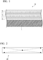
- a multilayer film 10 according to this embodiment is formed on a surface of a glass substrate 1, and includes Ag alloy films 11 and transparent dielectric films 12 formed on both surfaces of the Ag alloy film 11.
- the multilayer film 10 according to this embodiment has a structure of (2n+1) layers (n is the number of Ag alloy films 11). In this embodiment, two Ag alloy films 11 are formed, and the entire structure is a five-layer structure.
- each Ag alloy film 11 is, for example, in a range of 5 nm to 30 nm.
- each transparent dielectric film 12 is, for example, in a range of 5 nm to 200 nm.
- the transparent dielectric film 12 functions as an optical adjustment layer, and is formed of an oxide film or a nitride film containing at least one selected from Zn, Al, Sn, Ti, Si, Zr, Ta, and In. Specific examples thereof include ZnO X , SnO X , ZnSnO X , AlO X , AlN X , TiO X , SiN X , ZrO X , TaO X , and InSnO X .
- the oxide film or the nitride film is preferably appropriately selected according to required characteristics.
- the Ag alloy film 11 has a composition in which at least one of Sn or Ge is contained in a range of 0.5 atom% to 8.0 atom% in total, a total content of Na, K, Ba, and Te is 50 ppm by mass or less, a carbon content is 50 ppm by mass or less, and a remainder contains Ag and unavoidable impurities.
- the Ag alloy film 11 according to this embodiment preferably contains at least one of Sn or Ge in a range of 0.5 atom% to 3.0 atom% in total.
- the Ag alloy film 11 further contains at least one additive element selected from Mg, Ca, and Sb, and in a case where a total content of the additive element is represented by X atom% and a total content of Sn and Ge is represented by Z atom%, a ratio X/Z is in a range of 0.02 ⁇ X/Z ⁇ 0.4.
- a noble metal (Au, Pt, Pd, Rh, Ir, Ru, Os) may be further appropriately added to the Ag alloy film 11.
- the Ag alloy film 11 according to this embodiment is formed by a sputtering method using an Ag alloy sputtering target 20.
- the Ag alloy sputtering target 20 has the same composition as the above-described Ag alloy film 11. From the result of the component analysis of the formed Ag alloy film 11 by ICP emission spectroscopic analysis, the Ag alloy film is confirmed to have a composition substantially equivalent to that of the Ag alloy sputtering target 20.
- compositions of the Ag alloy film 11 and the Ag alloy sputtering target 20 are specified as described above will be shown below.
- Sn or Ge is an element that exists at crystal grain boundaries or in grains of the Ag film during heating of the film and suppresses the movement and aggregation of Ag atoms due to heat by a pinning effect, thereby improving the heat resistance of the Ag alloy film 11. It is possible to suppress the occurrence of defects such as cracks in the Ag alloy film 11 even in a case where the Ag alloy film 11 is heat-treated under a relatively high temperature condition such as 700°C. In addition, it is possible to improve the optical characteristics and the electrical characteristics of the Ag alloy film 11 and the Ag alloy sputtering target 20 after the heat treatment.
- the above-described actions and effects may not be achieved.
- the total content of at least one of Sn or Ge is greater than 8.0 atom%, the hardness of the alloy significantly increases, and cracks frequently occur during rolling or the like, whereby the Ag alloy sputtering target 20 for forming the Ag alloy film 11 may not be produced.
- the total content of at least one of Sn or Ge is in a range of 0.5 atom% to 8.0 atom%.
- the total content of at least one of Sn or Ge is preferably in a range of 0.5 atom% to 3.0 atom%.
- low-emission glass or the like includes tempered glass products that are strengthened by a heat treatment and ordinary glass products that are not heat-treated.
- tempered glass products that are strengthened by a heat treatment
- ordinary glass products that are not heat-treated.
- the optical characteristics and the electrical characteristics before the heat treatment can be improved, and tempered glass products and ordinary glass products can be produced without distinction.
- Na, K, Ba, and Te are elements that have a melting point of 700°C or lower and are not solid-soluted in Ag. Accordingly, in a case where the heat treatment is performed after the film formation, the above-described elements that have been solid-soluted in the mother phase of Ag in the Ag alloy film 11 may be concentrated at crystal grain boundaries and melted during the heating, and thus the characteristics of the Ag alloy film 11 may deteriorate.
- the total content of Na, K, Ba, and Te is limited to 50 ppm by mass or less, and the deterioration of the characteristics of the Ag alloy film 11 is suppressed.
- Carbon may be oxidized during the heat treatment and released as a CO gas or a CO 2 gas, that may cause unevenness in the Ag alloy film 11.
- the carbon content is limited to 50 ppm by mass or less to suppress the occurrence of unevenness in the Ag alloy film 11 due to the heat treatment or the like.
- the above-described additive elements act to further improve the heat resistance of the Ag alloy.
- the heat resistance may not be improved by the above-described additive element.
- X/Z is greater than 0.4, the heat resistance improving effect of Sn or Ge may be inhibited.
- the ratio X/Z is set in a range of 0.02 to 0.4.
- an area of a sputtering surface is 0.25 m 2 or greater.
- an average crystal grain size ⁇ GS in the sputtering surface is 200 ⁇ m or less, and a distribution D GS defined by the following expression by a standard deviation ⁇ GS of the crystal grain size and the average crystal grain size ⁇ GS is 25% or less.
- D GS ( ⁇ GS / ⁇ GS ) ⁇ 100 (%)
- the crystal grain size is measured at 5 positions, that is, the center and 4 corners of the sputtering surface, and from the obtained 5 measured values, the average crystal grain size ⁇ GS and the standard deviation ⁇ GS of the crystal grain size in the sputtering surface of the Ag alloy sputtering target 20 are calculated.
- the area of the sputtering surface of the Ag alloy sputtering target 20 is preferably 0.25 m 2 or greater.
- the average crystal grain size ⁇ GS in the sputtering surface is set to 200 ⁇ m or less, it is possible to suppress the occurrence of abnormal discharge during sputtering, and it is possible to stably perform the film formation by sputtering.
- the distribution D GS defined by the standard deviation ⁇ GS of the crystal grain size and the average crystal grain size ⁇ GS is limited to 25% or less.
- an Ag material having a purity of 99.9 mass% or greater and auxiliary materials Sn, Ge, Mg, Ca, and Sb having a purity of 99.9 mass% or greater are prepared.
- the Ag material is leached with a nitric acid, and electrolytic refining is performed using an electrolytic solution having a predetermined Ag concentration.
- the total content of Na, K, Ba, and Te is reduced to 50 ppm by mass or less, and the carbon content is reduced to 50 ppm by mass or less.
- the Ag material is dissolved under a vacuum atmosphere or an inert gas atmosphere, and a predetermined amount of Sn, Ge, Mg, Ca, and Sb is added to the obtained molten metal to produce an Ag alloy ingot having a predetermined composition.
- Sn, Ge, Mg, Ca, and Sb are preferably added in a state in which the Ag material is dissolved under a vacuum atmosphere, and then the atmosphere is replaced by an inert gas (Ar).
- a mother alloy containing the above-described elements may be used as an auxiliary material.
- the Ag alloy ingot is heat-treated by being held for 1 hour to 10 hours at a temperature of 600°C to 900°C.
- the heat treatment temperature is lower than 600°C or the holding time is shorter than 1 hour, sufficient homogenization may not be achieved.
- the heat treatment temperature is higher than 900°C, the temperature approaches the melting point of Ag, and softening and melting may occur.
- the holding time is longer than 10 hours, the auxiliary materials in the Ag alloy may be internally oxidized.
- hot working is performed.
- hot rolling is performed.
- the rolling finishing temperature is preferably in a range of 500°C to 700°C, and intermediate annealing is preferably performed depending on the circumstances.
- At least the working rate (rolling reduction) of the final one pass of rolling is preferably 20% or greater. In a case where the working rate (rolling reduction) is less than 20%, the crystal grain size cannot be sufficiently reduced, and the crystal grain size inside the alloy may be non-uniform. It is realistic that the working rate (rolling reduction) per pass is 50% or less from the relationship with the capacity of the rolling machine.
- the heat treatment temperature is preferably in a range of 600°C to 750°C
- the holding time is preferably in a range of 1 hour to 5 hours.
- the heat treatment temperature is lower than 600°C, a sufficient work hardening removing effect is not obtained, and in a case where the heat treatment temperature is higher than 750°C, the crystal grains may coarsen.
- rapid cooling is performed by air cooling or water cooling.
- the Ag alloy sputtering target 20 according to this embodiment is produced through the above-described steps.
- the transparent dielectric film 12 is formed on the surface of the glass substrate 1.
- the film is formed using a sputtering target made of the above-described oxide or nitride.
- a sputtering target made of the above-described oxide or nitride.
- the Ag alloy film 11 is formed on the formed transparent dielectric film 12 using the above-described Ag alloy sputtering target 20 according to this embodiment.
- the formation of the transparent dielectric film 12 and the Ag alloy film 11 as described above is repeated to form the multilayer film 10 according to this embodiment.
- the Ag alloy film 11 contains at least one of Sn or Ge in a range of 0.5 atom% to 8.0 atom% in total, and thus the heat resistance of the Ag alloy film 11 can be improved. Accordingly, it is not required to form a protective film made of a metal.
- the total content of Na, K, Ba, and Te in the Ag alloy film 11 is limited to 50 ppm by mass or less, it is possible to suppress the concentration of the elements at crystal grain boundaries during the heat treatment, and thus it is possible to suppress a deterioration of the characteristics of the Ag alloy film 11.
- the carbon content of the Ag alloy film 11 is limited to 50 ppm by mass or less, it is possible to suppress the release of carbon as a CO gas or a CO 2 gas during the heat treatment, and thus it is possible to suppress the occurrence of unevenness in the Ag alloy film 11.
- the optical characteristics and the electrical characteristics of the Ag alloy film 11 before the heat treatment can be improved, and tempered glass products and ordinary glass products can be produced without distinction.
- the Ag alloy film 11 further contains one or more additive elements selected from Mg, Ca, and Sb, and a relationship of X atom% representing a total content of the additive element with Z atom% representing a total content of Sn and Ge is in a range of 0.02 ⁇ X/Z ⁇ 0.4, the heat resistance of the Ag alloy film 11 can be further improved.
- the transparent dielectric film 12 is an oxide film or a nitride film containing at least one selected from Zn, Al, Sn, Ti, Si, Zr, Ta, and In, the transparent dielectric film 12 is excellent in optical characteristics such as visible light transmittance and electrical characteristics, and the optical characteristics and the electrical characteristics of the multilayer film 10 can be improved.
- the Ag alloy sputtering target 20 according to this embodiment has a composition equivalent to that of the above-described Ag alloy film 11, it is possible to form an Ag alloy film 11 having excellent heat resistance, optical characteristics, and electrical characteristics.
- the area of the sputtering surface is 0.25 m 2 or greater, and this is relatively large.
- the film formation by sputtering can be favorably performed on a large substrate or the like.
- the Ag alloy sputtering target 20 according to this embodiment has an average crystal grain size ⁇ GS of 200 ⁇ m or less in the sputtering surface, it is possible to suppress the occurrence of abnormal discharge during sputtering, and it is possible to stably perform the film formation by sputtering.
- the distribution D GS defined by the standard deviation ⁇ GS of the crystal grain size and the average crystal grain size ⁇ GS is 25% or less, it is possible to suppress variations in sputtering rate in the sputtering surface even after the sputtering has proceeded, and it is possible to form an Ag alloy film with little variation in thickness.
- low-emission glass in which a multilayer film is formed on a glass substrate has been described as an example, but the present invention is not limited thereto.
- a multilayer film according to this embodiment may be formed on a resin substrate, a resin film, or the like, and the resulting laminate may be used as a transparent conductive wiring film.
- a multilayer film having a five-layer structure including transparent dielectric films with two Ag alloy films formed as shown in Fig. 1 has been described, but the present invention is not limited thereto.
- a multilayer film having a three-layer structure in which one Ag alloy film is formed and a transparent dielectric film is formed on both surfaces of the Ag alloy film, or a multilayer film in which three or more Ag alloy films are formed and a transparent dielectric film is formed on both surfaces of each Ag alloy film may be provided.
- a transparent dielectric film formed using a sputtering target formed of oxide and nitride has been described, but the present invention is not limited thereto.
- the transparent dielectric film may be formed by performing reaction sputtering in an oxygen atmosphere or a nitrogen atmosphere using a sputtering target formed of the above-described metal (Zn, Al, Sn, Ti, Si, Zr, Ta, In).
- a sputtering surface having a rectangular shape has been described, but the present invention is not limited thereto.
- the sputtering surface may be circular, or a cylindrical sputtering target having a cylindrical sputtering surface may be used.
- Ag materials having a purity of 99.9 mass% or greater were prepared, and in Invention Examples and Comparative Examples 1 to 4, the Ag material was leached with a nitric acid, and then subjected to electrolytic refining using an electrolytic solution having a predetermined Ag concentration.
- the Ag material subjected to refining was subjected to impurity analysis and carbon gas analysis by an ICP method, and those with a total content of Na, K, Ba, and Te of 50 ppm by mass or less and a carbon content of 50 ppm by mass or less were used.
- Comparative Examples 5 and 6 those not subjected to the above-described electrolytic refining were used.
- Comparative Examples 7 and 8 Na, K, and C were appropriately added.
- the Ag material was dissolved in a vacuum atmosphere, the atmosphere was replaced by an Ar gas, and then auxiliary materials Sn, Ge, Mg, Ca, and Sb having a purity of 99.9 mass% or greater were added to obtain a molten Ag alloy having a predetermined composition. Then, the molten Ag alloy was cast, and thus an Ag alloy ingot was produced.
- the obtained Ag alloy ingot was homogenized under conditions of 700°C ⁇ 3 hours. After the homogenization treatment, hot rolling was performed. The rolling finishing temperature was 600°C, and the rolling reduction of the final one pass of rolling was 25%. After the hot rolling, a heat treatment was performed under conditions of 600°C ⁇ 1 hour.
- a plate having a length of 2,000 mm, a width of 200 mm, and a thickness of 8 mm was obtained in the above manner.
- Invention Example 19 a plate subjected to the post-hot-rolling heat treatment under conditions of 800°C ⁇ 3 hours was produced, and as Invention Example 20, a plate subjected to the homogenization treatment under conditions of 600°C ⁇ 30 minutes and the post-hot-rolling heat treatment under conditions of 800°C ⁇ 10 minutes was produced.
- a measurement sample was collected from the positions shown in Fig. 2 .
- a sputtering surface of each measurement sample was polished by waterproof abrasive paper of #180 to #4000 as an observation surface, and then buffed using abrasive grains of 1 to 3 ⁇ m.
- the sample was immersed for 1 to 2 seconds at room temperature in the etching liquid to perform etching of the observation surface.
- the observation surface after the etching was photographed by an optical microscope at a magnification of 30 times.
- a total of four 60 mm-line segments were vertically and horizontally drawn at intervals of 20 mm in a lattice shape, and the number of crystal grains cut by each straight line was counted.
- the number of crystal grains positioned at an end portion of the line segment was counted as 0.5.
- the above-described plate was cut and machined to produce an Ag alloy sputtering target having predetermined dimensions (126 mm ⁇ 178 mm ⁇ thickness 6 mm). Elements such as Na, K, and C exist in sebum and the like in a human body. Accordingly, the Ag alloy sputtering target was not handled with bare hands throughout the production process.
- the Ag alloy sputtering target was soldered to a backing plate made of oxygen-free copper, and this was mounted on a sputtering device.
- a magnetron DC sputtering device was used.
- a substrate transfer type sputtering device was used.
- the above-described target complex was attached to a usual magnetron sputtering device, and after the air was exhausted to 1 ⁇ 10 -4 Pa, the sputtering was performed under conditions of Ar gas pressure: 0.5 Pa, input power: DC 1000 W, and distance from target substrate: 60 mm.
- the abnormal discharge frequency during the sputtering was measured as abnormal discharge frequency for one hour from the start of discharge by an arc count function of a DC power supply (RPDG-50A) manufactured by MKS Instruments.
- Sputtering targets each formed of nitride and oxide shown in Tables 2 and 3 were prepared.
- ZnSnO X used for the first and third layers shown in Tables 2 and 3, the atom ratio of Zn:Sn was 1:1.
- the sputtering conditions for the Ag alloy film were specified as follows.
- Multilayer films of Invention Examples and Comparative Examples were formed in the above manner.
- a multilayer film having a layer configuration shown in Table 3 was formed.
- the multilayer films obtained as described above were heat-treated at 700°C for 5 minutes, and then air-cooled. Sheet resistance, visible light transmittance, and infrared reflectance before and after the heat treatment were measured as follows. In addition, the appearance of the multilayer films after the heat treatment was evaluated.
- the sheet resistance of the multilayer film was measured by a four probe method using a resistance measuring device (LORESTA GP manufactured by Mitsubishi Chemical Corporation). The evaluation results are shown in Tables 4 and 5.
- Fig. 3A shows the appearance observation result of Invention Example 3
- Fig. 3A shows the appearance observation result of Comparative Example 1.
- the multilayer films of Invention Examples 101 to 128 formed using the Ag alloy sputtering targets of Invention Examples 1 to 18, respectively, were confirmed to be excellent in sheet resistance after the heat treatment, visible light transmittance, and infrared reflectance.
- the appearance of the multilayer film after the heat treatment was evaluated as "A".
- the multilayer films of Invention Examples 113 and 119 to 128 formed using the Ag alloy sputtering target of Invention Example 13 were confirmed to be excellent in sheet resistance after the heat treatment, visible light transmittance, and infrared reflectance even in a case where the material of the transparent dielectric film was changed or in a case where the layer structure was a five-layer structure.
Landscapes
- Chemical & Material Sciences (AREA)
- Engineering & Computer Science (AREA)
- Organic Chemistry (AREA)
- Chemical Kinetics & Catalysis (AREA)
- Materials Engineering (AREA)
- Mechanical Engineering (AREA)
- Metallurgy (AREA)
- Life Sciences & Earth Sciences (AREA)
- General Chemical & Material Sciences (AREA)
- Geochemistry & Mineralogy (AREA)
- Inorganic Chemistry (AREA)
- Physics & Mathematics (AREA)
- Thermal Sciences (AREA)
- General Engineering & Computer Science (AREA)
- Physical Vapour Deposition (AREA)
Abstract
Description
- The present invention relates to, for example, a multilayer film that can be used as a heat shield film of low-emission glass that reflects infrared rays to shield heat or as a transparent conductive wiring film of a display or a touch panel, and an Ag alloy sputtering target that is used in the formation of an Ag alloy film constituting the multilayer film.
- Priority is claimed on
Japanese Patent Application No. 2017-076938, filed April 7, 2017 - In general, the above-described low-emission glass or the like has, for example, a structure in which a multilayer film (heat shield film) in which an Ag alloy film and a transparent dielectric film are laminated is formed on a glass surface as disclosed in Patent Literature 1. The multilayer film used in the low-emission glass or the like is required to have high infrared reflectance and high visible light transmittance.
- Such a multilayer film is also used as, for example, a transparent conductive wiring film for various displays and the like as described in Patent Literature 2. The transparent conductive wiring film is required to have high light transmittance in a visible light region and low electrical resistance.
- In the formation of an Ag alloy film on a glass substrate or the like, for example, a sputtering method using an Ag alloy sputtering target is used as disclosed in Patent Literatures 3 and 4.
-
- [Patent Literature 1]
Japanese Unexamined Patent Application, First Publication No. 2007-070146 - [Patent Literature 2]
Japanese Unexamined Patent Application, First Publication No. H09-232278 - [Patent Literature 3]
Japanese Unexamined Patent Application, First Publication No. 2004-238648 - [Patent Literature 4]
Japanese Unexamined Patent Application, First Publication No. 2006-240289 - In a case where the above-described multilayer film is used as a heat shield film, the film is required to have optical characteristics for transmitting visible light and reflecting infrared rays. In a case where the multilayer film is used as a transparent conductive wiring film, the film is required to have optical characteristics for transmitting visible light and electrical characteristics for obtaining an excellent conductivity.
- For example, in the production of low-emission glass or the like, for the purpose of strengthening the glass, a heat treatment (air cooling strengthening method) including heating to, for example, 700°C and rapid cooling by air or the like may be performed in a state in which a multilayer film is formed. In the above-described multilayer film, the Ag alloy film may be cracked during the heat treatment. For this reason, a protective film such as a metal film is formed on both surfaces of the Ag alloy film to improve the durability of the Ag alloy film. However, due to the formation of the protective film, problems such as an increase of the production cost and a deterioration of the optical characteristics may occur.
- In the production of a transparent conductive wiring film for various displays and the like, the process may also include the heat treatment.
- The present invention is contrived in view of the above-described circumstances, and an object thereof is to provide a multilayer film having excellent heat resistance, optical characteristics, and electrical characteristics, and an Ag alloy sputtering target that is used in the formation of an Ag alloy film constituting the multilayer film.
- In order to solve the problems, a multilayer film according to the present invention includes: an Ag alloy film; and a transparent dielectric film laminated on both surfaces of the Ag alloy film, and the Ag alloy film has a composition in which at least one of Sn or Ge is contained in a range of 0.5 atom% to 8.0 atom% in total, a total content of Na, K, Ba, and Te is 50 ppm by mass or less, a carbon content is 50 ppm by mass or less, and a remainder contains Ag and unavoidable impurities.
- In the multilayer film according to the present invention, since the Ag alloy film contains at least one of Sn or Ge in a range of 0.5 atom% to 8.0 atom% in total, the heat resistance of the Ag alloy film can be improved. Accordingly, it is not required to form a protective film made of a metal.
- Na, K, Ba, and Te are elements that have a relatively low melting point of 700°C or lower and are unlikely to be solid-soluted in Ag. Therefore, by limiting the total content of Na, K, Ba, and Te to 50 ppm by mass or less in the Ag alloy film, it is possible to suppress the concentration of the elements at grain boundaries due to a heat treatment or the like.
- Carbon may be oxidized during the heat treatment and released as a CO gas or a CO2 gas, that may cause unevenness in the Ag alloy film. Accordingly, by limiting the carbon content of the Ag alloy film to 50 ppm by mass or less, it is possible to suppress the occurrence of unevenness in the Ag alloy film due to the heat treatment or the like.
- Therefore, in the multilayer film according to the present invention, even in a case where a heat treatment is performed under a relatively high temperature condition such as 700°C, it is possible to suppress the occurrence of cracks in the Ag alloy film.
- In addition, the multilayer film according to the present invention is excellent in optical characteristics such as visible light transmittance and infrared reflectance, and is also excellent in electrical characteristics such as conductivity.
- In the multilayer film according to the present invention, it is preferable that the Ag alloy film contains at least one of Sn or Ge in a range of 0.5 atom% to 3.0 atom% in total.
- In this case, since the upper limit of the total content of at least one of Sn or Ge is 3.0 atom% or less, it is possible to further improve the optical characteristics and the electrical characteristics of the multilayer film.
- In the multilayer film according to the present invention, the Ag alloy film further contains at least one additive element selected from Mg, Ca, and Sb, a total content of the additive element is represented by X atom%, and a total content of Sn and Ge is represented by Z atom%. In this case, it is preferable that the ratio X/Z is in a range of 0.02 ≤ X/Z ≤ 0.4.
- Since the Ag alloy film contains Mg, Ca, and Sb in the above range, the heat resistance of the Ag alloy film can be further improved.
- In the multilayer film according to the present invention, it is preferable that the transparent dielectric film is an oxide film or a nitride film containing at least one selected from Zn, Al, Sn, Ti, Si, Zr, Ta, and In.
- In this case, the transparent dielectric film is excellent in optical characteristics such as visible light transmittance and electrical characteristics, and the optical characteristics and the electrical characteristics of the multilayer film can be improved.
- An Ag alloy sputtering target according to the present invention has a composition in which at least one of Sn or Ge is contained in a range of 0.5 atom% to 8.0 atom% in total, a total content of Na, K, Ba, and Te is 50 ppm by mass or less, a carbon content is 50 ppm by mass or less, and a remainder contains Ag and unavoidable impurities. As described above, with the Ag alloy sputtering target having the above configuration, it is possible to form an Ag alloy film having excellent heat resistance, optical characteristics, and electrical characteristics.
- In the Ag alloy sputtering target according to the present invention, it is preferable that at least one of Sn or Ge is contained in a range of 0.5 atom% to 3.0 atom% in total.
- In this case, since the upper limit of the total content of at least one of Sn or Ge is 3.0 atom% or less, it is possible to form an Ag alloy film that is more excellent in optical characteristics and electrical characteristics of a multilayer film.
- In the Ag alloy sputtering target according to the present invention, it is preferable that at least one additive element selected from Mg, Ca, and Sb is further contained, and in a case where a total content of the additive element is represented by X atom% and a total content of Sn and Ge is represented by Z atom%, a ratio X/Z is in a range of 0.02 ≤ X/Z ≤ 0.4.
- Since Mg, Ca, and Sb are contained in the above range, the heat resistance of an Ag alloy film formed can be further improved.
- In the Ag alloy sputtering target according to the present invention, it is preferable that an area of a sputtering surface is 0.25 m2 or greater, an average crystal grain size µGS in the sputtering surface is 200 µm or less, and a distribution DGS defined by the following expression by a standard deviation σGS of the crystal grain size and the average crystal grain size µGS is 25% or less.

- In this case, even in a case where the area of the sputtering surface is a large area of 0.25 m2 or greater, the average crystal grain size µGS in the sputtering surface is 200 µm or less, and thus it is possible to suppress the occurrence of abnormal discharge during sputtering. In addition, since the distribution DGS defined by the standard deviation σGS of the crystal grain size and the average crystal grain size µGS is 25% or less, it is possible to suppress variations in sputtering rate in the sputtering surface even after the sputtering has proceeded, and it is possible to form an Ag alloy film with little variation in thickness.
- It is possible to provide a multilayer film having excellent heat resistance, optical characteristics, and electrical characteristics, and an Ag alloy sputtering target that is used in the formation of an Ag alloy film constituting the multilayer film.
-
-
Fig. 1 is a cross-sectional view illustrating a multilayer film according to an embodiment of the present invention. -
Fig. 2 is an illustration showing positions where a crystal grain size is measured in a sputtering surface of an Ag alloy sputtering target according to the embodiment of the present invention. -
Fig. 3A is a photograph showing an observation result of the appearance of a multilayer film of Invention Example 3 after a heat treatment in Examples. -
Fig. 3B is a photograph showing an observation result of the appearance of a multilayer film of Comparative Example 1 after a heat treatment in Examples. - Hereinafter, a multilayer film and an Ag alloy sputtering target according to one embodiment of this invention will be described. The multilayer film according to this embodiment is formed on a surface of a glass substrate, and constitutes low-emission glass that reflects infrared rays to shield heat.
- As shown in
Fig. 1 , amultilayer film 10 according to this embodiment is formed on a surface of a glass substrate 1, and includes Ag alloy films 11 and transparentdielectric films 12 formed on both surfaces of the Ag alloy film 11. Themultilayer film 10 according to this embodiment has a structure of (2n+1) layers (n is the number of Ag alloy films 11). In this embodiment, two Ag alloy films 11 are formed, and the entire structure is a five-layer structure. - The film thickness of each Ag alloy film 11 is, for example, in a range of 5 nm to 30 nm.
- The film thickness of each
transparent dielectric film 12 is, for example, in a range of 5 nm to 200 nm. - It is preferable that the
transparent dielectric film 12 functions as an optical adjustment layer, and is formed of an oxide film or a nitride film containing at least one selected from Zn, Al, Sn, Ti, Si, Zr, Ta, and In. Specific examples thereof include ZnOX, SnOX, ZnSnOX, AlOX, AlNX, TiOX, SiNX, ZrOX, TaOX, and InSnOX. - The oxide film or the nitride film is preferably appropriately selected according to required characteristics.
- The Ag alloy film 11 has a composition in which at least one of Sn or Ge is contained in a range of 0.5 atom% to 8.0 atom% in total, a total content of Na, K, Ba, and Te is 50 ppm by mass or less, a carbon content is 50 ppm by mass or less, and a remainder contains Ag and unavoidable impurities. The Ag alloy film 11 according to this embodiment preferably contains at least one of Sn or Ge in a range of 0.5 atom% to 3.0 atom% in total.
- It is preferable that the Ag alloy film 11 further contains at least one additive element selected from Mg, Ca, and Sb, and in a case where a total content of the additive element is represented by X atom% and a total content of Sn and Ge is represented by Z atom%, a ratio X/Z is in a range of 0.02 ≤ X/Z ≤ 0.4.
- A noble metal (Au, Pt, Pd, Rh, Ir, Ru, Os) may be further appropriately added to the Ag alloy film 11.
- The Ag alloy film 11 according to this embodiment is formed by a sputtering method using an Ag
alloy sputtering target 20. - The Ag
alloy sputtering target 20 has the same composition as the above-described Ag alloy film 11. From the result of the component analysis of the formed Ag alloy film 11 by ICP emission spectroscopic analysis, the Ag alloy film is confirmed to have a composition substantially equivalent to that of the Agalloy sputtering target 20. - The reasons why the compositions of the Ag alloy film 11 and the Ag
alloy sputtering target 20 are specified as described above will be shown below. - Sn or Ge is an element that exists at crystal grain boundaries or in grains of the Ag film during heating of the film and suppresses the movement and aggregation of Ag atoms due to heat by a pinning effect, thereby improving the heat resistance of the Ag alloy film 11. It is possible to suppress the occurrence of defects such as cracks in the Ag alloy film 11 even in a case where the Ag alloy film 11 is heat-treated under a relatively high temperature condition such as 700°C. In addition, it is possible to improve the optical characteristics and the electrical characteristics of the Ag alloy film 11 and the Ag
alloy sputtering target 20 after the heat treatment. - In a case where the total content of at least one of Sn or Ge is less than 0.5 atom%, the above-described actions and effects may not be achieved. In contrast, in a case where the total content of at least one of Sn or Ge is greater than 8.0 atom%, the hardness of the alloy significantly increases, and cracks frequently occur during rolling or the like, whereby the Ag
alloy sputtering target 20 for forming the Ag alloy film 11 may not be produced. - Therefore, in this embodiment, the total content of at least one of Sn or Ge is in a range of 0.5 atom% to 8.0 atom%.
- The total content of at least one of Sn or Ge is preferably in a range of 0.5 atom% to 3.0 atom%.
- For example, low-emission glass or the like includes tempered glass products that are strengthened by a heat treatment and ordinary glass products that are not heat-treated. By limiting the total content of at least one of Sn or Ge to 3.0 atom% or less, the optical characteristics and the electrical characteristics before the heat treatment can be improved, and tempered glass products and ordinary glass products can be produced without distinction.
- Na, K, Ba, and Te are elements that have a melting point of 700°C or lower and are not solid-soluted in Ag. Accordingly, in a case where the heat treatment is performed after the film formation, the above-described elements that have been solid-soluted in the mother phase of Ag in the Ag alloy film 11 may be concentrated at crystal grain boundaries and melted during the heating, and thus the characteristics of the Ag alloy film 11 may deteriorate.
- Therefore, in this embodiment, the total content of Na, K, Ba, and Te is limited to 50 ppm by mass or less, and the deterioration of the characteristics of the Ag alloy film 11 is suppressed.
- Carbon may be oxidized during the heat treatment and released as a CO gas or a CO2 gas, that may cause unevenness in the Ag alloy film 11.
- Accordingly, in this embodiment, the carbon content is limited to 50 ppm by mass or less to suppress the occurrence of unevenness in the Ag alloy film 11 due to the heat treatment or the like.
- The above-described additive elements act to further improve the heat resistance of the Ag alloy.
- In a case where a ratio X/Z of X atom% representing a total content of at least one additive element selected from Mg, Ca, and Sb to Z atom% representing a total content of Sn and Ge is less than 0.02, the heat resistance may not be improved by the above-described additive element. In a case where X/Z is greater than 0.4, the heat resistance improving effect of Sn or Ge may be inhibited.
- Therefore, in this embodiment, in a case where a total content of one or more additive elements selected from Mg, Ca, and Sb is represented by X atom% and a total content of Sn and Ge is represented by Z atom%, the ratio X/Z is set in a range of 0.02 to 0.4.
- In the Ag
alloy sputtering target 20 according to this embodiment, an area of a sputtering surface is 0.25 m2 or greater. In addition, an average crystal grain size µGS in the sputtering surface is 200 µm or less, and a distribution DGS defined by the following expression by a standard deviation σGS of the crystal grain size and the average crystal grain size µGS is 25% or less. DGS = (σGS/µGS) × 100 (%) - In this embodiment, since the sputtering surface has a rectangular shape as shown in
Fig. 2 , the crystal grain size is measured at 5 positions, that is, the center and 4 corners of the sputtering surface, and from the obtained 5 measured values, the average crystal grain size µGS and the standard deviation σGS of the crystal grain size in the sputtering surface of the Agalloy sputtering target 20 are calculated. - The reasons why the area of the sputtering surface and the crystal grain size in the sputtering surface of the Ag
alloy sputtering target 20 are specified as described above will be shown below. - In order to produce glass as a building material, it is necessary to form a multilayer film 10 (Ag alloy film 11) with a relatively large area. Accordingly, the area of the sputtering surface of the Ag
alloy sputtering target 20 is preferably 0.25 m2 or greater. - By setting the average crystal grain size µGS in the sputtering surface to 200 µm or less, it is possible to suppress the occurrence of abnormal discharge during sputtering, and it is possible to stably perform the film formation by sputtering.
- In a case where a crystal grain size distribution exists in the sputtering surface, a difference in sputtering rate may occur in the sputtering surface in the sputtering performed for a long period of time, and a film thickness distribution may occur in the formed Ag alloy film 11. Therefore, the distribution DGS defined by the standard deviation σGS of the crystal grain size and the average crystal grain size µGS is limited to 25% or less.
- Next, a method of producing the Ag
alloy sputtering target 20 according to this embodiment will be described. - First, an Ag material having a purity of 99.9 mass% or greater and auxiliary materials Sn, Ge, Mg, Ca, and Sb having a purity of 99.9 mass% or greater are prepared.
- The Ag material is leached with a nitric acid, and electrolytic refining is performed using an electrolytic solution having a predetermined Ag concentration. The total content of Na, K, Ba, and Te is reduced to 50 ppm by mass or less, and the carbon content is reduced to 50 ppm by mass or less.
- The Ag material is dissolved under a vacuum atmosphere or an inert gas atmosphere, and a predetermined amount of Sn, Ge, Mg, Ca, and Sb is added to the obtained molten metal to produce an Ag alloy ingot having a predetermined composition. Sn, Ge, Mg, Ca, and Sb are preferably added in a state in which the Ag material is dissolved under a vacuum atmosphere, and then the atmosphere is replaced by an inert gas (Ar). Further, a mother alloy containing the above-described elements may be used as an auxiliary material.
- Next, as a homogenization treatment step, the Ag alloy ingot is heat-treated by being held for 1 hour to 10 hours at a temperature of 600°C to 900°C.
- In a case where the heat treatment temperature is lower than 600°C or the holding time is shorter than 1 hour, sufficient homogenization may not be achieved. In a case where the heat treatment temperature is higher than 900°C, the temperature approaches the melting point of Ag, and softening and melting may occur. In a case where the holding time is longer than 10 hours, the auxiliary materials in the Ag alloy may be internally oxidized.
- Next, hot working is performed. In this embodiment, hot rolling is performed. The rolling finishing temperature is preferably in a range of 500°C to 700°C, and intermediate annealing is preferably performed depending on the circumstances.
- At least the working rate (rolling reduction) of the final one pass of rolling is preferably 20% or greater. In a case where the working rate (rolling reduction) is less than 20%, the crystal grain size cannot be sufficiently reduced, and the crystal grain size inside the alloy may be non-uniform. It is realistic that the working rate (rolling reduction) per pass is 50% or less from the relationship with the capacity of the rolling machine.
- Next, after the hot rolling, a heat treatment is performed to homogenize the crystal structure of the sputtering target and to remove work hardening. The heat treatment temperature is preferably in a range of 600°C to 750°C, and the holding time is preferably in a range of 1 hour to 5 hours.
- In a case where the heat treatment temperature is lower than 600°C, a sufficient work hardening removing effect is not obtained, and in a case where the heat treatment temperature is higher than 750°C, the crystal grains may coarsen. After the heat treatment, rapid cooling is performed by air cooling or water cooling.
- The Ag
alloy sputtering target 20 according to this embodiment is produced through the above-described steps. - Next, a method of producing the
multilayer film 10 according to this embodiment will be described. - First, the
transparent dielectric film 12 is formed on the surface of the glass substrate 1. In this embodiment, the film is formed using a sputtering target made of the above-described oxide or nitride. In consideration of the conductive property of the sputtering target, direct current (DC) sputtering, radio frequency (RF) sputtering, medium frequency (MF) sputtering, alternating current (AC) sputtering, or the like is preferably appropriately selected and used. - The Ag alloy film 11 is formed on the formed
transparent dielectric film 12 using the above-described Agalloy sputtering target 20 according to this embodiment. - The formation of the
transparent dielectric film 12 and the Ag alloy film 11 as described above is repeated to form themultilayer film 10 according to this embodiment. - In the
multilayer film 10 according to this embodiment having the above configuration, the Ag alloy film 11 contains at least one of Sn or Ge in a range of 0.5 atom% to 8.0 atom% in total, and thus the heat resistance of the Ag alloy film 11 can be improved. Accordingly, it is not required to form a protective film made of a metal. - Since the total content of Na, K, Ba, and Te in the Ag alloy film 11 is limited to 50 ppm by mass or less, it is possible to suppress the concentration of the elements at crystal grain boundaries during the heat treatment, and thus it is possible to suppress a deterioration of the characteristics of the Ag alloy film 11.
- Since the carbon content of the Ag alloy film 11 is limited to 50 ppm by mass or less, it is possible to suppress the release of carbon as a CO gas or a CO2 gas during the heat treatment, and thus it is possible to suppress the occurrence of unevenness in the Ag alloy film 11.
- Accordingly, even in a case where a heat treatment is performed under a relatively high temperature condition such as 700°C, it is possible to suppress the occurrence of cracks in the Ag alloy film 11, and a
multilayer film 10 having excellent optical characteristics and electrical characteristics can be provided. - In the Ag alloy film 11, in a case where the total content of at least one of Sn or Ge is 0.5 atom% to 3.0 atom%, the optical characteristics and the electrical characteristics of the Ag alloy film 11 before the heat treatment can be improved, and tempered glass products and ordinary glass products can be produced without distinction.
- In a case where the Ag alloy film 11 further contains one or more additive elements selected from Mg, Ca, and Sb, and a relationship of X atom% representing a total content of the additive element with Z atom% representing a total content of Sn and Ge is in a range of 0.02 ≤ X/Z ≤ 0.4, the heat resistance of the Ag alloy film 11 can be further improved.
- In this embodiment, since the
transparent dielectric film 12 is an oxide film or a nitride film containing at least one selected from Zn, Al, Sn, Ti, Si, Zr, Ta, and In, thetransparent dielectric film 12 is excellent in optical characteristics such as visible light transmittance and electrical characteristics, and the optical characteristics and the electrical characteristics of themultilayer film 10 can be improved. - Since the Ag
alloy sputtering target 20 according to this embodiment has a composition equivalent to that of the above-described Ag alloy film 11, it is possible to form an Ag alloy film 11 having excellent heat resistance, optical characteristics, and electrical characteristics. - In the Ag
alloy sputtering target 20 according to this embodiment, the area of the sputtering surface is 0.25 m2 or greater, and this is relatively large. Thus, the film formation by sputtering can be favorably performed on a large substrate or the like. - Since the Ag
alloy sputtering target 20 according to this embodiment has an average crystal grain size µGS of 200 µm or less in the sputtering surface, it is possible to suppress the occurrence of abnormal discharge during sputtering, and it is possible to stably perform the film formation by sputtering. - In the Ag
alloy sputtering target 20 according to this embodiment, since the distribution DGS defined by the standard deviation σGS of the crystal grain size and the average crystal grain size µGS is 25% or less, it is possible to suppress variations in sputtering rate in the sputtering surface even after the sputtering has proceeded, and it is possible to form an Ag alloy film with little variation in thickness. - Although the embodiments of the present invention have been described as above, the present invention is not limited thereto, and can be appropriately changed without departing from the technical idea of the present invention.
- For example, in this embodiment, low-emission glass in which a multilayer film is formed on a glass substrate has been described as an example, but the present invention is not limited thereto. A multilayer film according to this embodiment may be formed on a resin substrate, a resin film, or the like, and the resulting laminate may be used as a transparent conductive wiring film.
- In this embodiment, a multilayer film having a five-layer structure including transparent dielectric films with two Ag alloy films formed as shown in
Fig. 1 has been described, but the present invention is not limited thereto. A multilayer film having a three-layer structure in which one Ag alloy film is formed and a transparent dielectric film is formed on both surfaces of the Ag alloy film, or a multilayer film in which three or more Ag alloy films are formed and a transparent dielectric film is formed on both surfaces of each Ag alloy film may be provided. - In this embodiment, a transparent dielectric film formed using a sputtering target formed of oxide and nitride has been described, but the present invention is not limited thereto. The transparent dielectric film may be formed by performing reaction sputtering in an oxygen atmosphere or a nitrogen atmosphere using a sputtering target formed of the above-described metal (Zn, Al, Sn, Ti, Si, Zr, Ta, In).
- In this embodiment, a sputtering surface having a rectangular shape has been described, but the present invention is not limited thereto. The sputtering surface may be circular, or a cylindrical sputtering target having a cylindrical sputtering surface may be used.
- Hereinafter, results of experiments for confirmation performed to confirm the effectiveness of the present invention will be described.
- Ag materials having a purity of 99.9 mass% or greater were prepared, and in Invention Examples and Comparative Examples 1 to 4, the Ag material was leached with a nitric acid, and then subjected to electrolytic refining using an electrolytic solution having a predetermined Ag concentration.
- The Ag material subjected to refining was subjected to impurity analysis and carbon gas analysis by an ICP method, and those with a total content of Na, K, Ba, and Te of 50 ppm by mass or less and a carbon content of 50 ppm by mass or less were used. In Comparative Examples 5 and 6, those not subjected to the above-described electrolytic refining were used. In Comparative Examples 7 and 8, Na, K, and C were appropriately added.
- The Ag material was dissolved in a vacuum atmosphere, the atmosphere was replaced by an Ar gas, and then auxiliary materials Sn, Ge, Mg, Ca, and Sb having a purity of 99.9 mass% or greater were added to obtain a molten Ag alloy having a predetermined composition. Then, the molten Ag alloy was cast, and thus an Ag alloy ingot was produced. The obtained Ag alloy ingot was homogenized under conditions of 700°C × 3 hours. After the homogenization treatment, hot rolling was performed. The rolling finishing temperature was 600°C, and the rolling reduction of the final one pass of rolling was 25%. After the hot rolling, a heat treatment was performed under conditions of 600°C × 1 hour.
- A plate having a length of 2,000 mm, a width of 200 mm, and a thickness of 8 mm was obtained in the above manner.
- In addition, as Invention Example 19, a plate subjected to the post-hot-rolling heat treatment under conditions of 800°C × 3 hours was produced, and as Invention Example 20, a plate subjected to the homogenization treatment under conditions of 600°C × 30 minutes and the post-hot-rolling heat treatment under conditions of 800°C × 10 minutes was produced.
- In the obtained plate, an average crystal grain size and a distribution in a sputtering surface were measured as follows.
- A measurement sample was collected from the positions shown in
Fig. 2 . A sputtering surface of each measurement sample was polished by waterproof abrasive paper of #180 to #4000 as an observation surface, and then buffed using abrasive grains of 1 to 3 µm. - Then, using a mixed liquid of hydrogen peroxide water and ammonia water as an etching liquid, the sample was immersed for 1 to 2 seconds at room temperature in the etching liquid to perform etching of the observation surface.
- The observation surface after the etching was photographed by an optical microscope at a magnification of 30 times. In each photograph, a total of four 60 mm-line segments were vertically and horizontally drawn at intervals of 20 mm in a lattice shape, and the number of crystal grains cut by each straight line was counted. The number of crystal grains positioned at an end portion of the line segment was counted as 0.5.
- An average cut piece length L (µm) was calculated by L = 60,000/(M·N). M is actual magnification, and N is the average number of cut crystal grains.
- With the average cut piece length L, a crystal grain size d (µm) of the measurement sample was calculated by d = (3/2) × L.
- An average crystal grain size µGS and a standard deviation σGS of the crystal grain size of the whole plate were calculated from a 5-point average of the crystal grain sizes obtained from the measurement samples at 5 positions. Using the average crystal grain size µGS and the standard deviation σGS of the crystal grain size, a distribution DGS was calculated by the following expression. The measurement results are shown in Table 1.

- Next, the above-described plate was cut and machined to produce an Ag alloy sputtering target having predetermined dimensions (126 mm × 178 mm × thickness 6 mm). Elements such as Na, K, and C exist in sebum and the like in a human body. Accordingly, the Ag alloy sputtering target was not handled with bare hands throughout the production process.
- The Ag alloy sputtering target was soldered to a backing plate made of oxygen-free copper, and this was mounted on a sputtering device. In this embodiment, a magnetron DC sputtering device was used. In this embodiment, a substrate transfer type sputtering device was used.
- The above-described target complex was attached to a usual magnetron sputtering device, and after the air was exhausted to 1 × 10⁻⁴ Pa, the sputtering was performed under conditions of Ar gas pressure: 0.5 Pa, input power: DC 1000 W, and distance from target substrate: 60 mm. The abnormal discharge frequency during the sputtering was measured as abnormal discharge frequency for one hour from the start of discharge by an arc count function of a DC power supply (RPDG-50A) manufactured by MKS Instruments.
- In the plate having the above-described dimensions (2,000 mm × 200 mm × 8 mmt), three Ag alloy sputtering targets having predetermined dimensions (126 mm × 178 mm × 6 mm) were produced from three positions (left end, center, right end) in the longitudinal direction. Each sputtering target was sputtered under the same conditions as in paragraph 0063, and a sputtering rate was calculated. In order to calculate the sputtering rate, a film was formed for a certain period of time on a glass substrate covered with a mask tape for measuring a step, and a step of the formed film was measured using a step measuring device (ULVAC, Inc., DEKTAK-XT). The difference in sputtering rate among the three sputtering targets was calculated by the following expression.

- Sputtering targets each formed of nitride and oxide shown in Tables 2 and 3 were prepared. In ZnSnOX used for the first and third layers shown in Tables 2 and 3, the atom ratio of Zn:Sn was 1:1.
- On a 5 cm square glass substrate (EAGLE XG glass manufactured by Corning Incorporated), a multilayer film having a layer configuration shown in Tables 2 and 3 was formed by sputtering.
- The sputtering conditions for the Ag alloy film were specified as follows.
- Vacuum at Which Film Formation is Started: 1.0 × 10⁻⁴ Pa or less
- Sputtering Gas: High-purity argon
- Sputtering Gas Pressure in Chamber: 0.5 Pa
- Direct Current: 300 W
- Multilayer films of Invention Examples and Comparative Examples were formed in the above manner. As a conventional example, a multilayer film having a layer configuration shown in Table 3 was formed.
- The multilayer films obtained as described above were heat-treated at 700°C for 5 minutes, and then air-cooled. Sheet resistance, visible light transmittance, and infrared reflectance before and after the heat treatment were measured as follows. In addition, the appearance of the multilayer films after the heat treatment was evaluated.
- The sheet resistance of the multilayer film was measured by a four probe method using a resistance measuring device (LORESTA GP manufactured by Mitsubishi Chemical Corporation). The evaluation results are shown in Tables 4 and 5.
- Using a spectrophotometer (U-4100 manufactured by Hitachi High-Technologies Corporation), the transmittance at a wavelength of 550 nm (visible light) and the reflectance at a wavelength of 2,000 nm (infrared rays) were measured. The evaluation results are shown in Tables 4 and 5.
- The appearance of the multilayer film after the heat treatment was observed using an optical microscope at an actual magnification of 100 times. Those in which defects of 100 µm or greater were observed were ranked as "B", and those in which no defects of 100 µm or greater were observed were ranked as "A". The evaluation results are shown in Table 3.
Fig. 3A shows the appearance observation result of Invention Example 3, andFig. 3A shows the appearance observation result of Comparative Example 1.[Table 1] Composition (atom%) Composition Ratio Impurities (ppm by mass) Crystal Grain Size Abnormal Discharge Frequency (frequency) Maximum Difference in Sputtering Rate (%) Sn Ge Ca Mg Sb Ag X/Z Na, K, Ba, Te c Average µGS (µm) Distribution DGS (%) 1 0.5 - - - - remainder - 8 10 170 11 1 3 2 3.0 - - - - remainder - 7 10 150 20 1 4 3 5.0 - - - - remainder - 6 20 110 12 1 3 4 8.0 - - - - remainder - 3 10 110 13 0 3 5 - 0.5 - - - remainder - 2 10 120 15 1 3 6 - 3.0 - - - remainder - 2 20 140 17 0 2 7 - 5.0 - - - remainder - 4 10 120 14 1 3 8 - 8.0 - - - remainder - 2 10 130 13 1 3 9 1.0 1.0 - - - remainder - 5 10 120 15 1 2 Invention Examples 10 3.0 - 0.2 - - remainder 0.07 6 10 80 17 1 3 11 3.0 - - 1.0 - remainder 0.33 4 20 100 15 0 2 12 3.0 - - - 0.5 remainder 0.17 6 10 90 20 1 3 13 - 2.0 0.1 - - remainder 0.05 2 10 80 17 0 4 14 - 3.0 0.2 - - remainder 0.07 3 10 70 14 0 3 15 - 3.0 - 1.0 - remainder 0.33 4 10 140 10 0 3 16 - 2.0 - 0.5 - remainder 0.25 4 20 110 14 0 3 17 - 3.0 - - 1.0 remainder 0.33 1 20 120 15 0 3 18 - 3.0 - - 0.5 remainder 0.17 4 10 90 16 0 3 19 - 2.0 0.1 - - remainder 0.05 3 10 310 16 25 3 20 - 2.0 0.1 - - remainder 0.05 2 10 260 41 22 10 Comparative Examples 1 0.1 - - - - remainder - 5 10 190 15 1 3 2 10.0 - - - - remainder - 4 10 Cracks occurred during production. 3 - 0.1 - - - remainder - 4 10 180 22 1 2 4 - 10.0 - - - remainder - 5 10 Cracks occurred during production. 5 3.0 - - - - remainder - 81 60 120 24 0 4 6 - 3.0 - - - remainder - 160 80 140 16 1 3 7 - 3.0 - - - remainder - 80 10 150 14 0 3 8 - 3.0 - - - remainder - 14 70 110 15 0 3 9 - 1.0 0.5 - - remainder 0.50 4 10 90 20 0 3 10 - 3.0 - 2.0 - remainder 0.67 5 10 110 15 1 3 11 - 3.0 - - 3.0 remainder 1.00 3 10 100 14 1 3 [Table 2] Layer Structure of Multilayer Film First Layer Second Layer Third Layer Fourth Layer Fifth Layer Sixth Layer Material Thickness (nm) Material Thickness (nm) Material Thickness (nm) Material Thickness (nm) Material Thickness (nm) Material Thickness (nm) 101 ZnSnOX 40 Invention Example 1 18 ZnSnOX 40 - - - - - - 102 ZnSnOX 40 Invention Example 2 18 ZnSnOX 40 - - - - - - 103 ZnSnOX 40 Invention Example 3 18 ZnSnOX 40 - - - - - - 104 ZnSnOX 40 Invention Example 4 18 ZnSnOX 40 - - - - - - 105 ZnSnOX 40 Invention Example 5 18 ZnSnOX 40 - - - - - - 106 ZnSnOX 40 Invention Example 6 18 ZnSnOX 40 - - - - - - 107 ZnSnOX 40 Invention Example 7 18 ZnSnOX 40 - - - - - - 108 ZnSnOX 40 Invention Example 8 18 ZnSnOX 40 - - - - - - 109 ZnSnOX 40 Invention Example 9 18 ZnSnOX 40 - - - - - - 110 ZnSnOX 40 Invention Example 10 18 ZnSnOX 40 - - - - - - 111 ZnSnOX 40 Invention Example 11 18 ZnSnOX 40 - - - - - - 112 ZnSnOX 40 Invention Example 12 18 ZnSnOX 40 - - - - - - 113 ZnSnOX 40 Invention Example 13 18 ZnSnOX 40 - - - - - - Invention Examples 114 ZnSnOX 40 Invention Example 14 18 ZnSnOX 40 - - - - - - 115 ZnSnOX 40 Invention Example 15 18 ZnSnOX 40 - - - - - - 116 ZnSnOX 40 Invention Example 16 18 ZnSnOX 40 - - - - - - 117 ZnSnOX 40 Invention Example 17 18 ZnSnOX 40 - - - - - - 118 ZnSnOX 40 Invention Example 18 18 ZnSnOX 40 - - - - - - 119 ZnOX 40 Invention Example 13 18 ZnOX 40 - - - - - - 120 SnOX 40 Invention Example 13 18 SnOX 40 - - - - - - 121 AlOX 40 Invention Example 13 18 AlOX 40 - - - - - - 122 AlNX 40 Invention Example 13 18 AlNX 40 - - - - - - 123 TiOX 40 Invention Example 13 18 TiOX 40 - - - - - - 124 SiNX 40 Invention Example 13 18 SiNX 40 - - - - - - 125 ZrOX 40 Invention Example 13 18 ZrOX 40 - - - - - - 126 TaOX 40 Invention Example 13 18 TaOX 40 - - - - - - 127 InSnOX 40 Invention Example 13 18 InSnOX 40 - - - - - - 128 ZnSnOX 40 Invention Example 13 11 ZnSnOX 80 Invention Example 13 14 ZnSnOX 40 - - [Table 3] Layer Structure of Multilayer Film First Layer Second Layer Third Layer Fourth Layer Fifth Layer Sixth Layer Material Thickness (nm) Material Thickness (nm) Material Thickness (nm) Material Thickness (nm) Material Thickness (nm) Material Thickness (nm) Comparative Examples 101 ZnSnOX 40 Comparative Example 1 18 ZnSnOX 40 - - - - - - 103 ZnSnOX 40 Comparative Example 3 18 ZnSnOX 40 - - - - - - 105 ZnSnOX 40 Comparative Example 5 18 ZnSnOX 40 - - - - - - 106 ZnSnOX 40 Comparative Example 6 18 ZnSnOX 40 - - - - - - 107 ZnSnOX 40 Comparative Example 7 18 ZnSnOX 40 - - - - - - 108 ZnSnOX 40 Comparative Example 8 18 ZnSnOX 40 - - - - - - 109 ZnSnOX 40 Comparative Example 9 18 ZnSnOX 40 - - - - - - 110 ZnSnOX 40 Comparative Example 10 18 ZnSnOX 40 - - - - - - 111 ZnSnOX 40 Comparative Example 11 18 ZnSnOX 40 - - - - - - Conventional Example SnO2 32 ZnO·Al 5 pure Ag 10 Zn·Al 2 ZnO· Al 10 SnO2 25 [Table 4] Before Heat Treatment After Heat Treatment Sheet Resistance (Ω/□) Visible Light Transmittance (%) Infrared Reflectance (%) Sheet Resistance (Ω/□) Visible Light Transmittance (%) Infrared Reflectance (%) Appearance Observation 101 3.5 76.9 90.0 2.4 81.5 91.0 A 102 6.6 73.4 89.5 2.2 82.0 91.0 A 103 9.6 68.6 86.5 2.1 82.1 92.0 A 104 12.1 66.7 85.4 2.1 82.3 92.1 A 105 3.3 77.0 90.1 2.5 81.6 91.7 A 106 5.9 74.8 89.7 2.3 82.1 91.6 A 107 9.0 69.1 86.2 2.0 82.3 91.4 A 108 11.5 67.8 85.8 2.0 82.4 92.0 A 109 4.5 75.0 90.0 2.3 82.0 92.0 A 110 6.6 73.4 87.0 2.2 83.0 92.1 A 111 6.8 73.1 86.9 2.1 82.9 92.4 A 112 6.9 73.5 87.5 2.1 83.1 92.4 A 113 4.7 75.4 88.3 2.2 83.0 92.4 A Invention Examples 114 6.0 74.5 89.0 2.2 83.2 92.0 A 115 6.5 74.7 88.1 2.1 83.4 92.1 A 116 5.9 75.3 88.3 2.2 83.5 92.4 A 117 6.7 74.6 88.3 2.4 83.4 92.3 A 118 6.4 74.2 88.4 2.2 83.3 92.1 A 119 4.6 74.4 88.2 2.1 81.9 92.2 A 120 4.8 70.1 88.3 2.4 82.0 92.4 A 121 4.5 70.0 88.4 2.2 84.0 92.2 A 122 4.7 75.9 88.3 2.3 83.4 92.2 A 123 4.9 77.1 88.4 2.1 84.0 92.2 A 124 5.0 76.8 88.3 2.3 83.8 92.1 A 125 5.1 76.4 88.3 2.4 83.7 92.1 A 126 5.1 76.7 88.3 2.3 83.8 92.3 A 127 4.7 78.0 88.4 2.2 83.9 92.0 A 128 2.1 82.0 91.5 1.5 85.1 93.6 A [Table 5] Before Heat Treatment After Heat Treatment Sheet Resistance (Ω/□) Visible Light Transmittance (%) Infrared Reflectance (%) Sheet Resistance (Ω/□) Visible Light Transmittance (%) Infrared Reflectance (%) Appearance Observation Comparative Examples 101 3.1 77.1 90.0 5.0 75.2 84.1 B 103 3.0 77.3 90.1 5.2 74.3 83.2 B 105 6.7 73.5 89.4 10.2 64.1 80.1 B 106 6.3 75.1 89.5 9.8 63.1 80.0 B 107 6.4 75.3 89.5 10.2 70.0 83.2 B 108 6.3 75.1 89.6 9.9 68.6 81.6 B 109 3.7 76.5 89.7 4.5 66.6 81.4 B 110 6.9 73.9 88.4 7.0 68.0 81.3 B 111 10.0 72.1 87.5 10.1 68.2 82.0 B Conventional Example 6.6 78.1 81.0 6.8 74.1 80.0 B - The multilayer films of Comparative Examples 101 and 103 using the Ag alloy sputtering targets of Comparative Examples 1 and 3, respectively, in which the total content of at least one of Sn or Ge was less than 0.5 atom% were confirmed to deteriorate in sheet resistance after the heat treatment, visible light transmittance, and infrared reflectance. In addition, the appearance of the multilayer film after the heat treatment was evaluated as "B".
- In Comparative Examples 2 and 4 in which the total content of at least one Sn or Ge was greater than 8.0 atom%, cracks occurred during the production of the target, and thus it was not possible to produce the Ag alloy sputtering target. Therefore, the subsequent evaluation was stopped.
- The multilayer films of Comparative Examples 105 to 108 formed using the Ag alloy sputtering targets of Comparative Examples 5 and 6 in which the total content of Na, K, Ba, and Te was greater than 50 ppm by mass and the carbon content was greater than 50 ppm by mass, Comparative Example 7 in which the total content of Na, K, Ba, and Te was greater than 50 ppm by mass, and Comparative Example 8 in which the carbon content was greater than 50 ppm by mass, respectively, were confirmed to deteriorate in sheet resistance after the heat treatment, visible light transmittance, and infrared reflectance. In addition, the appearance of the multilayer film after the heat treatment was evaluated as "B".
- The multilayer films of Comparative Examples 109 to 111 formed using the Ag alloy sputtering targets of Comparative Examples 9 to 11 in which the ratio X/Z of the total content X atom% of one or more additive elements selected from Mg, Ca, and Sb to the total content Z atom% of Sn and Ge was greater than 0.5, respectively, were confirmed to deteriorate in sheet resistance after the heat treatment, visible light transmittance, and infrared reflectance. In addition, the appearance of the multilayer film after the heat treatment was evaluated as "B".
- In contrast, the multilayer films of Invention Examples 101 to 128 formed using the Ag alloy sputtering targets of Invention Examples 1 to 18, respectively, were confirmed to be excellent in sheet resistance after the heat treatment, visible light transmittance, and infrared reflectance. In addition, the appearance of the multilayer film after the heat treatment was evaluated as "A". Furthermore, the multilayer films of Invention Examples 113 and 119 to 128 formed using the Ag alloy sputtering target of Invention Example 13 were confirmed to be excellent in sheet resistance after the heat treatment, visible light transmittance, and infrared reflectance even in a case where the material of the transparent dielectric film was changed or in a case where the layer structure was a five-layer structure. Moreover, in Invention Examples 1 to 18 in which the average crystal grain size µGS in the sputtering surface was 200 µm or less and the distribution DGS was 25% or less, the abnormal discharge frequency was low, and the in-plane difference in sputtering rate was small.
- From the above, it has been confirmed that according to Invention Examples, it is possible to provide a multilayer film having excellent heat resistance, optical characteristics, and electrical characteristics, and an Ag alloy sputtering target that is used in the formation of an Ag alloy film constituting the multilayer film.
- It is possible to provide a multilayer film having excellent heat resistance, optical characteristics, and electrical characteristics, and an Ag alloy sputtering target that is used in the formation of an Ag alloy film constituting the multilayer film.
-
- 10
- Multilayer film
- 11
- Ag alloy film
- 12
- Transparent dielectric film
- 20
- Ag alloy sputtering target
Claims (8)
- A multilayer film comprising:an Ag alloy film; anda transparent dielectric film laminated on both surfaces of the Ag alloy film,wherein the Ag alloy film has a composition in which at least one of Sn or Ge is contained in a range of 0.5 atom% to 8.0 atom% in total, a total content of Na, K, Ba, and Te is 50 ppm by mass or less, a carbon content is 50 ppm by mass or less, and a remainder contains Ag and unavoidable impurities.
- The multilayer film according to claim 1,
wherein the Ag alloy film contains at least one of Sn or Ge in a range of 0.5 atom% to 3.0 atom% in total. - The multilayer film according to claim 1 or 2,
wherein the Ag alloy film further contains at least one additive element selected from Mg, Ca, and Sb, and
in a case where a total content of the additive element is represented by X atom% and a total content of Sn and Ge is represented by Z atom%, a ratio X/Z is in a range of 0.02 ≤ X/Z ≤ 0.4. - The multilayer film according to any one of claims 1 to 3,
wherein the transparent dielectric film is an oxide film or a nitride film containing at least one selected from Zn, Al, Sn, Ti, Si, Zr, Ta, and In. - An Ag alloy sputtering target having a composition in which at least one of Sn or Ge is contained in a range of 0.5 atom% to 8.0 atom% in total, a total content of Na, K, Ba, and Te is 50 ppm by mass or less, a carbon content is 50 ppm by mass or less, and a remainder contains Ag and unavoidable impurities.
- The Ag alloy sputtering target according to claim 5,
wherein at least one of Sn or Ge is contained in a range of 0.5 atom% to 3.0 atom% in total. - The Ag alloy sputtering target according to claim 5 or 6,
wherein at least one additive element selected from Mg, Ca, and Sb is further contained, and
in a case where a total content of the additive element is represented by X atom% and a total content of Sn and Ge is represented by Z atom%, a ratio X/Z is in a range of 0.02 ≤ X/Z ≤ 0.4. - The Ag alloy sputtering target according to any one of claims 5 to 7,
wherein an area of a sputtering surface is 0.25 m2 or greater, an average crystal grain size µGS in the sputtering surface is 200 µm or less, and a distribution DGS defined by the following expression by a standard deviation σGS of the crystal grain size and the average crystal grain size µGS is 25% or less.
Applications Claiming Priority (1)
| Application Number | Priority Date | Filing Date | Title |
|---|---|---|---|
| PCT/JP2018/037025 WO2020070824A1 (en) | 2018-10-03 | 2018-10-03 | Multilayer film, and ag alloy sputtering target |
Publications (2)
| Publication Number | Publication Date |
|---|---|
| EP3862459A1 true EP3862459A1 (en) | 2021-08-11 |
| EP3862459A4 EP3862459A4 (en) | 2022-05-11 |
Family
ID=70055184
Family Applications (1)
| Application Number | Title | Priority Date | Filing Date |
|---|---|---|---|
| EP18936160.3A Withdrawn EP3862459A4 (en) | 2018-10-03 | 2018-10-03 | Multilayer film, and ag alloy sputtering target |
Country Status (5)
| Country | Link |
|---|---|
| US (1) | US20210310113A1 (en) |
| EP (1) | EP3862459A4 (en) |
| KR (1) | KR20210070264A (en) |
| CN (1) | CN112752863A (en) |
| WO (1) | WO2020070824A1 (en) |
Cited By (2)
| Publication number | Priority date | Publication date | Assignee | Title |
|---|---|---|---|---|
| US20220145697A1 (en) * | 2019-07-25 | 2022-05-12 | AGC Inc. | Laminated body and method of manufacturing laminated body |
| WO2023066491A1 (en) * | 2021-10-21 | 2023-04-27 | Mimsi Materials Ab | Low emissivity glazing and methods of its production |
Family Cites Families (15)
| Publication number | Priority date | Publication date | Assignee | Title |
|---|---|---|---|---|
| JP3558301B2 (en) * | 1993-04-22 | 2004-08-25 | 三菱マテリアル株式会社 | High corrosion resistant Ag-Mg alloy thin film |
| JPH073435A (en) * | 1993-04-22 | 1995-01-06 | Mitsubishi Materials Corp | High corrosion resistance Ag-Mg alloy and thin film thereof |
| JP3521600B2 (en) | 1996-02-21 | 2004-04-19 | 旭硝子株式会社 | Method for patterning transparent conductive film and substrate with transparent electrode |
| JP2004002929A (en) * | 2001-08-03 | 2004-01-08 | Furuya Kinzoku:Kk | Silver alloys, sputtering targets, reflectors for reflective LCDs, reflective wiring electrodes, thin films, their manufacturing methods, optical recording media, electromagnetic wave shields, metal materials for electronic components, wiring materials, electronic components, electronic devices, metal film processing Method, electro-optical component, laminate and building material glass |
| JP2004238648A (en) | 2003-02-04 | 2004-08-26 | Hitachi Metals Ltd | Ag alloy film for electronic component, flat panel display, and sputtering target material for forming Ag alloy film for electronic component |
| JP4605494B2 (en) * | 2004-05-20 | 2011-01-05 | 日立金属株式会社 | Ag alloy sputtering target material |
| JP2006240289A (en) | 2005-02-07 | 2006-09-14 | Kobe Steel Ltd | Recording film for optical information recording medium, optical information recording medium and sputtering target |
| JP2007070146A (en) | 2005-09-06 | 2007-03-22 | Nippon Sheet Glass Co Ltd | Low emissive multilayered glass |
| US8815149B2 (en) * | 2005-12-29 | 2014-08-26 | Mitsubishi Materials Corporation | Semi-reflective film and reflective film for optical recording medium, and Ag alloy sputtering target for forming semi-reflective film or reflective film for optical recording medium |
| SG193986A1 (en) * | 2011-04-06 | 2013-11-29 | Mitsubishi Materials Corp | Silver alloy sputtering target for forming electroconductive film, and method for manufacture same |
| JP5159963B1 (en) * | 2012-01-13 | 2013-03-13 | 三菱マテリアル株式会社 | Silver alloy sputtering target for forming conductive film and method for producing the same |
| WO2016043183A1 (en) * | 2014-09-18 | 2016-03-24 | 三菱マテリアル株式会社 | Ag ALLOY SPUTTERING TARGET, MANUFACTURING METHOD FOR Ag ALLOY SPUTTERING TARGET, Ag ALLOY FILM, AND MANUFACTURING METHOD FOR ALLOY FILM |
| JP6801264B2 (en) * | 2015-07-28 | 2020-12-16 | 三菱マテリアル株式会社 | Ag alloy film and its manufacturing method, Ag alloy sputtering target and laminated film |
| JP6659111B2 (en) | 2015-10-16 | 2020-03-04 | キヤノン株式会社 | Information processing device |
| JP2018176493A (en) * | 2017-04-07 | 2018-11-15 | 三菱マテリアル株式会社 | Laminated film and Ag alloy sputtering target |
-
2018
- 2018-10-03 US US17/276,517 patent/US20210310113A1/en not_active Abandoned
- 2018-10-03 WO PCT/JP2018/037025 patent/WO2020070824A1/en not_active Ceased
- 2018-10-03 CN CN201880098094.7A patent/CN112752863A/en active Pending
- 2018-10-03 EP EP18936160.3A patent/EP3862459A4/en not_active Withdrawn
- 2018-10-03 KR KR1020217003957A patent/KR20210070264A/en not_active Ceased
Cited By (3)
| Publication number | Priority date | Publication date | Assignee | Title |
|---|---|---|---|---|
| US20220145697A1 (en) * | 2019-07-25 | 2022-05-12 | AGC Inc. | Laminated body and method of manufacturing laminated body |
| US12246986B2 (en) * | 2019-07-25 | 2025-03-11 | AGC Inc. | Laminated body and method of manufacturing laminated body |
| WO2023066491A1 (en) * | 2021-10-21 | 2023-04-27 | Mimsi Materials Ab | Low emissivity glazing and methods of its production |
Also Published As
| Publication number | Publication date |
|---|---|
| EP3862459A4 (en) | 2022-05-11 |
| CN112752863A (en) | 2021-05-04 |
| KR20210070264A (en) | 2021-06-14 |
| WO2020070824A1 (en) | 2020-04-09 |
| US20210310113A1 (en) | 2021-10-07 |
Similar Documents
| Publication | Publication Date | Title |
|---|---|---|
| JP6801264B2 (en) | Ag alloy film and its manufacturing method, Ag alloy sputtering target and laminated film | |
| EP2803754B1 (en) | Silver-alloy sputtering target for conductive-film formation, and method for producing same | |
| EP3196333B1 (en) | Ag alloy sputtering target and manufacturing method for ag alloy film | |
| KR101679562B1 (en) | silver alloy composition forming conductive membrane and manufacturing method of it | |
| KR101854009B1 (en) | Silver-alloy sputtering target for conductive-film formation, and method for producing same | |
| EP3795713A1 (en) | Multilayer film and ag alloy sputtering target | |
| JP2022008503A (en) | Laminated film and Ag alloy sputtering target | |
| KR20100108236A (en) | Method for preparing cu alloy layer containing oxygen | |
| KR20210010451A (en) | Laminated film and Ag alloy sputtering target | |
| US20210310113A1 (en) | Multilayer film, and ag alloy sputtering target | |
| CN107075614A (en) | Cu alloy films and Cu stacked films | |
| CN107614745B (en) | Aluminum alloy sputtering target material | |
| TWI673374B (en) | Sputtering target and layered film | |
| JP2019131850A (en) | Laminated film and Ag alloy sputtering target | |
| EP3922748A1 (en) | Ag alloy sputtering target, and ag alloy film | |
| EP3922747A1 (en) | Ag alloy sputtering target, and ag alloy film | |
| WO2016043183A1 (en) | Ag ALLOY SPUTTERING TARGET, MANUFACTURING METHOD FOR Ag ALLOY SPUTTERING TARGET, Ag ALLOY FILM, AND MANUFACTURING METHOD FOR ALLOY FILM | |
| EP3892752A1 (en) | Metal film and sputtering target | |
| EP3892753A1 (en) | Metal film and sputtering target | |
| WO2021090581A1 (en) | Ag ALLOY SPUTTERING TARGET AND Ag ALLOY FILM | |
| JPWO2016132578A1 (en) | Copper-based alloy sputtering target |
Legal Events
| Date | Code | Title | Description |
|---|---|---|---|
| STAA | Information on the status of an ep patent application or granted ep patent |
Free format text: STATUS: THE INTERNATIONAL PUBLICATION HAS BEEN MADE |
|
| PUAI | Public reference made under article 153(3) epc to a published international application that has entered the european phase |
Free format text: ORIGINAL CODE: 0009012 |
|
| STAA | Information on the status of an ep patent application or granted ep patent |
Free format text: STATUS: REQUEST FOR EXAMINATION WAS MADE |
|
| 17P | Request for examination filed |
Effective date: 20210315 |
|
| AK | Designated contracting states |
Kind code of ref document: A1 Designated state(s): AL AT BE BG CH CY CZ DE DK EE ES FI FR GB GR HR HU IE IS IT LI LT LU LV MC MK MT NL NO PL PT RO RS SE SI SK SM TR |
|
| DAV | Request for validation of the european patent (deleted) | ||
| DAX | Request for extension of the european patent (deleted) | ||
| A4 | Supplementary search report drawn up and despatched |
Effective date: 20220412 |
|
| RIC1 | Information provided on ipc code assigned before grant |
Ipc: C23C 14/34 20060101ALI20220406BHEP Ipc: C23C 14/08 20060101ALI20220406BHEP Ipc: C03C 17/36 20060101ALI20220406BHEP Ipc: B32B 15/04 20060101ALI20220406BHEP Ipc: B32B 9/00 20060101ALI20220406BHEP Ipc: C23C 14/06 20060101AFI20220406BHEP |
|
| STAA | Information on the status of an ep patent application or granted ep patent |
Free format text: STATUS: THE APPLICATION IS DEEMED TO BE WITHDRAWN |
|
| 18D | Application deemed to be withdrawn |
Effective date: 20221115 |