WO2016043183A1 - Ag ALLOY SPUTTERING TARGET, MANUFACTURING METHOD FOR Ag ALLOY SPUTTERING TARGET, Ag ALLOY FILM, AND MANUFACTURING METHOD FOR ALLOY FILM - Google Patents
Ag ALLOY SPUTTERING TARGET, MANUFACTURING METHOD FOR Ag ALLOY SPUTTERING TARGET, Ag ALLOY FILM, AND MANUFACTURING METHOD FOR ALLOY FILM Download PDFInfo
- Publication number
- WO2016043183A1 WO2016043183A1 PCT/JP2015/076124 JP2015076124W WO2016043183A1 WO 2016043183 A1 WO2016043183 A1 WO 2016043183A1 JP 2015076124 W JP2015076124 W JP 2015076124W WO 2016043183 A1 WO2016043183 A1 WO 2016043183A1
- Authority
- WO
- WIPO (PCT)
- Prior art keywords
- alloy
- film
- atomic
- sputtering target
- less
- Prior art date
Links
Images
Classifications
-
- C—CHEMISTRY; METALLURGY
- C22—METALLURGY; FERROUS OR NON-FERROUS ALLOYS; TREATMENT OF ALLOYS OR NON-FERROUS METALS
- C22C—ALLOYS
- C22C5/00—Alloys based on noble metals
- C22C5/06—Alloys based on silver
-
- C—CHEMISTRY; METALLURGY
- C22—METALLURGY; FERROUS OR NON-FERROUS ALLOYS; TREATMENT OF ALLOYS OR NON-FERROUS METALS
- C22F—CHANGING THE PHYSICAL STRUCTURE OF NON-FERROUS METALS AND NON-FERROUS ALLOYS
- C22F1/00—Changing the physical structure of non-ferrous metals or alloys by heat treatment or by hot or cold working
- C22F1/14—Changing the physical structure of non-ferrous metals or alloys by heat treatment or by hot or cold working of noble metals or alloys based thereon
-
- C—CHEMISTRY; METALLURGY
- C23—COATING METALLIC MATERIAL; COATING MATERIAL WITH METALLIC MATERIAL; CHEMICAL SURFACE TREATMENT; DIFFUSION TREATMENT OF METALLIC MATERIAL; COATING BY VACUUM EVAPORATION, BY SPUTTERING, BY ION IMPLANTATION OR BY CHEMICAL VAPOUR DEPOSITION, IN GENERAL; INHIBITING CORROSION OF METALLIC MATERIAL OR INCRUSTATION IN GENERAL
- C23C—COATING METALLIC MATERIAL; COATING MATERIAL WITH METALLIC MATERIAL; SURFACE TREATMENT OF METALLIC MATERIAL BY DIFFUSION INTO THE SURFACE, BY CHEMICAL CONVERSION OR SUBSTITUTION; COATING BY VACUUM EVAPORATION, BY SPUTTERING, BY ION IMPLANTATION OR BY CHEMICAL VAPOUR DEPOSITION, IN GENERAL
- C23C14/00—Coating by vacuum evaporation, by sputtering or by ion implantation of the coating forming material
- C23C14/06—Coating by vacuum evaporation, by sputtering or by ion implantation of the coating forming material characterised by the coating material
- C23C14/14—Metallic material, boron or silicon
-
- C—CHEMISTRY; METALLURGY
- C23—COATING METALLIC MATERIAL; COATING MATERIAL WITH METALLIC MATERIAL; CHEMICAL SURFACE TREATMENT; DIFFUSION TREATMENT OF METALLIC MATERIAL; COATING BY VACUUM EVAPORATION, BY SPUTTERING, BY ION IMPLANTATION OR BY CHEMICAL VAPOUR DEPOSITION, IN GENERAL; INHIBITING CORROSION OF METALLIC MATERIAL OR INCRUSTATION IN GENERAL
- C23C—COATING METALLIC MATERIAL; COATING MATERIAL WITH METALLIC MATERIAL; SURFACE TREATMENT OF METALLIC MATERIAL BY DIFFUSION INTO THE SURFACE, BY CHEMICAL CONVERSION OR SUBSTITUTION; COATING BY VACUUM EVAPORATION, BY SPUTTERING, BY ION IMPLANTATION OR BY CHEMICAL VAPOUR DEPOSITION, IN GENERAL
- C23C14/00—Coating by vacuum evaporation, by sputtering or by ion implantation of the coating forming material
- C23C14/22—Coating by vacuum evaporation, by sputtering or by ion implantation of the coating forming material characterised by the process of coating
- C23C14/34—Sputtering
-
- C—CHEMISTRY; METALLURGY
- C22—METALLURGY; FERROUS OR NON-FERROUS ALLOYS; TREATMENT OF ALLOYS OR NON-FERROUS METALS
- C22F—CHANGING THE PHYSICAL STRUCTURE OF NON-FERROUS METALS AND NON-FERROUS ALLOYS
- C22F1/00—Changing the physical structure of non-ferrous metals or alloys by heat treatment or by hot or cold working
Definitions
- the present invention relates to an Ag alloy sputtering target for forming an Ag alloy film applicable to, for example, a transparent conductive film for a display or a touch panel or a metal thin film of an optical functional film, a method for producing an Ag alloy sputtering target, and an Ag alloy film. And an Ag alloy film manufacturing method.
- patterned transparent conductive films are widely used in electronic devices such as touch panels, solar cells, and organic EL devices.
- Ag or an Ag alloy with an element added to Ag is a material having excellent electrical conductivity, and since excellent transmittance can be obtained when a thin film is formed, the transparent conductive film of these electronic devices can be obtained. Application to this is expected (see Patent Document 1).
- optical functional films are used in fields such as heat ray cutting and display devices.
- a high refractive index thin film made of a metal oxide is formed on one side of a transparent polymer film.
- a transparent laminated film called a so-called multilayer film type in which metal thin films are alternately laminated is known.
- Ag or an Ag alloy is also used as a material for the metal thin film of such an optical functional film (see Patent Document 2).
- Ag and an Ag alloy have a problem in that deterioration of characteristics caused by corrosion due to humidity, sulfur, etc. in the manufacturing process and the environment during use, and changes in film appearance (spots, etc.) are likely to occur.
- the film thickness is 15 nm or less as used for a semi-permeable film, they are particularly prominent, and the occurrence of spots due to film aggregation caused by particles adhering to the film surface becomes a problem.
- Patent Documents 3 and 4 propose Ag alloy films with improved environmental resistance.
- Patent Document 3 proposes an Ag alloy film in which a noble metal such as platinum, palladium, gold, rhodium, ruthenium, or iridium is added to Ag.
- Patent Document 4 proposes an Ag alloy film containing Bi and at least one selected from Zn, Al, Ga, In, Si, Ge, and Sn.
- the Ag alloy film described in Patent Document 3 has a drawback in that the material cost is high because a noble metal is used as the additive element.
- the Ag alloy film described in Patent Document 4 has a relatively high absorption rate and insufficient optical characteristics.
- a transparent conductive film used for an electronic device such as an organic EL device is also required to have excellent conductivity (electric properties).
- the present invention has been made in view of the above-described circumstances, and is an Ag alloy sputtering target capable of forming an Ag alloy film excellent in electrical characteristics, optical characteristics, and environmental resistance, a method for producing an Ag alloy sputtering target, Ag An object is to provide an alloy film and a method for producing an Ag alloy film.
- the Ag alloy sputtering target according to the first aspect of the present invention has Sn of 0.1 atomic% to 3.0 atomic% and Cu of 1.0 atomic% to 10.0 atoms. % Or less, with the balance being composed of Ag and inevitable impurities.
- Sn is within a range of 0.1 atomic% to 3.0 atomic% and Cu is within a range of 1.0 atomic% to 10.0 atomic%. Since it contains and the balance consists of Ag and inevitable impurities, Ag aggregation can be suppressed, and an Ag alloy film with greatly improved environmental resistance can be formed. Moreover, it can suppress that the optical characteristic of an Ag alloy film falls in a hot-humid environment by containing Sn. Furthermore, it can suppress that the electrical property of an Ag alloy film falls in a hot-humid environment by containing Cu.
- the total content of Na, Si, V, Cr, Fe, and Co among the inevitable impurities is preferably 100 mass ppm or less.
- the total content of Na, Si, V, Cr, Fe, and Co, which are elements having a low solid solubility with respect to Ag among the inevitable impurities is limited to 100 ppm by mass or less. Segregation at grain boundaries can be suppressed, and abnormal discharge during sputtering can be suppressed. Also, in the formed Ag alloy film, segregation of these elements to the crystal grain boundaries is suppressed, and the environmental resistance of the Ag alloy film can be suppressed from decreasing.
- the content of each of Na, Si, V, Cr, Fe, and Co among the inevitable impurities is 30 mass ppm or less. preferable.
- the content of each element of Na, Si, V, Cr, Fe, and Co, which is an element having a low solid solubility with respect to Ag is limited to 30 ppm by mass or less, so that abnormal discharge occurs during sputtering. Can be reliably suppressed.
- even in the formed Ag alloy film it is possible to reliably suppress a decrease in environmental resistance.
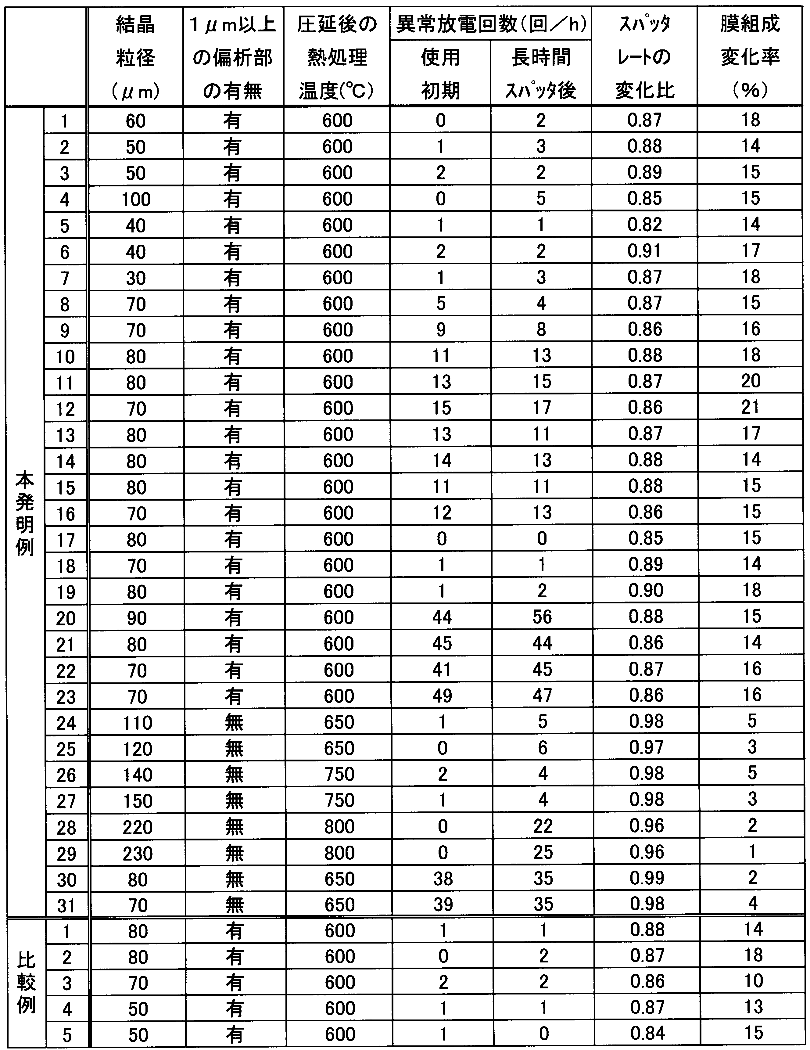
- the average crystal grain size on the sputtering surface is 200 ⁇ m or less, and the grain size of the segregation part made of Cu, Sn or an intermetallic compound thereof is 1 ⁇ m. It is preferable to be less than. In this case, since the average crystal grain size is 200 ⁇ m or less, the unevenness caused by the difference in the sputtering rate depending on the crystal orientation when the sputtering surface is consumed by sputtering can be reduced, and the occurrence of abnormal discharge is suppressed. be able to.
- the particle size of the segregation part made of Cu, Sn, or an intermetallic compound thereof is less than 1 ⁇ m, it is possible to stabilize the sputtering rate during long-time sputtering and the component composition in the deposited Ag alloy film. . In addition, it is more preferable that this segregation part does not exist in a structure
- tissue since the particle size of the segregation part made of Cu, Sn, or an intermetallic compound thereof is less than 1 ⁇ m, it is possible to stabilize the sputtering rate during long-time sputtering and the component composition in the deposited Ag alloy film. . In addition, it is more preferable that this segregation part does not exist in a structure
- the Ag alloy sputtering target according to the first aspect of the present invention it is preferable to further contain Ti in the range of 0.1 atomic% to 3.0 atomic%.
- Ti since 0.1 atomic% or more of Ti is added, the chemical resistance of the formed Ag alloy film can be greatly improved.
- the addition amount of Ti is limited to 3.0 atomic% or less, it is possible to suppress deterioration of optical characteristics and electrical characteristics of the formed Ag alloy film.
- the manufacturing method of the Ag alloy sputtering target according to the second aspect of the present invention is the above-described Ag alloy sputtering target (Sn is 0.1 atomic% or more and 3.0 atomic% or less, Cu is 1.0 atomic% or more and 10. Segregation which is contained within the range of 0 atomic% or less, the balance is composed of Ag and inevitable impurities, the average crystal grain size on the sputtering surface is 200 ⁇ m or less, and further composed of Cu, Sn or an intermetallic compound thereof.
- a heat treatment temperature in the heat treatment step is in a range of 650 ° C. or higher and 750 ° C. or lower. It is said.
- the heat treatment temperature in the heat treatment step is set to 650 ° C. or more, Cu and Sn can be diffused to eliminate segregation.
- the segregation part which consists of an intermetallic compound of this can be made small.
- the heat treatment temperature in the heat treatment step is 750 ° C. or lower, the coarsening of crystal grains can be suppressed.
- the Ag alloy film according to the third aspect of the present invention contains Sn in the range of 0.1 atomic% to 3.0 atomic% and Cu in the range of 1.0 atomic% to 10.0 atomic%, The remainder has a composition comprising Ag and inevitable impurities.
- Sn is contained in the range of 0.1 atomic% to 3.0 atomic%
- Cu is contained in the range of 1.0 atomic% to 10.0 atomic%, with the balance being Ag and Since it has a composition composed of inevitable impurities, it has excellent electrical characteristics, environmental resistance and optical characteristics, and is particularly suitable as a transparent conductive film, a metal thin film of an optical functional film, and the like.
- the luminous transmittance is preferably 70% or more and the luminous absorption rate is 10% or less. In this case, it will be excellent in visibility and can be used suitably as a transparent conductive film of various displays and touch panels, or a metal thin film of an optical functional film.
- the sheet resistance value is preferably 40 ⁇ / ⁇ or less. In this case, it can apply to the electrode film and wiring film of various displays and a touch panel as a transparent conductive film excellent in electroconductivity.
- the film thickness is preferably in the range of 4 nm to 10 nm.
- the thickness of the Ag alloy film is set to 4 nm or more, the electrical resistance can be reliably lowered and the conductivity can be ensured.
- the thickness of the Ag alloy film is 10 nm or less, the luminous transmittance can be improved with certainty.
- the method for producing an Ag alloy film according to the fourth aspect of the present invention is characterized in that a film is formed by the Ag alloy sputtering target according to the first aspect described above. According to the method for producing an Ag alloy film having this configuration, an Ag alloy film containing Cu and Sn and having excellent electrical characteristics, environmental resistance, and optical characteristics can be formed.
- the Ag alloy sputtering target which can form Ag alloy film excellent in an electrical property, an optical characteristic, and environmental resistance, the manufacturing method of Ag alloy sputtering target, Ag alloy film, and the manufacturing method of Ag alloy film are provided. It becomes possible to do.
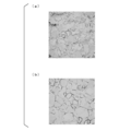
- tissue photograph of the Ag alloy sputtering target in an Example (A) is an Ag alloy sputtering target of Invention Example 1, and (b) is an Ag alloy sputtering target of Invention Example 26. It is an external appearance observation result of the Ag alloy film after the constant temperature and humidity test in an Example. (A) is determined as “A”, and (b) is determined as “B”.
- the Ag alloy sputtering target according to the present embodiment is used when an Ag alloy film is formed.
- the Ag alloy film according to the present embodiment is used as a transparent conductive film of an electronic device such as a touch panel, a solar battery, or an organic EL device, and a metal thin film of an optical functional film.
- the Ag alloy sputtering target according to the present embodiment contains Sn in the range of 0.1 atomic% to 3.0 atomic%, Cu in the range of 1.0 atomic% to 10.0 atomic%, with the balance being Ag. And an Ag alloy having a composition of inevitable impurities.
- the total content of Na, Si, V, Cr, Fe, and Co among the inevitable impurities is 100 mass ppm or less.
- each content of Na, Si, V, Cr, Fe, and Co among the inevitable impurities is set to 30 ppm by mass or less.
- Ti may be contained within a range of 0.1 atomic% to 3.0 atomic%.
- the average crystal grain size on the sputtering surface is set to 200 ⁇ m or less, and the grain size of the segregation part made of Cu, Sn, or an intermetallic compound thereof is set to less than 1 ⁇ m. ing.
- the reason why the composition and crystal structure of the Ag alloy sputtering target according to the present embodiment are defined as described above will be described below.
- Sn is an element having an effect of improving the environmental resistance of the formed Ag alloy film. In particular, it has the effect of effectively suppressing a decrease in optical properties in a hot and humid environment.
- the content of Sn in the Ag alloy sputtering target is less than 0.1 atomic%, the above-described effects may not be sufficiently achieved.
- the Sn content in the Ag alloy sputtering target exceeds 3.0 atomic%, the electrical characteristics of the formed Ag alloy film may be deteriorated.
- the Sn content in the Ag alloy sputtering target is set in the range of 0.1 atomic% to 3.0 atomic%.
- the lower limit of the Sn content in the Ag alloy sputtering target is 0.4 atomic% or more and the upper limit is 2.0 atomic% or less.
- Cu is an element having an effect of improving the environmental resistance of the formed Ag alloy film. In particular, it has the effect of effectively suppressing a decrease in electrical characteristics in a hot and humid environment. Moreover, it has the effect which suppresses generation
- the content of Cu in the Ag alloy sputtering target is less than 1.0 atomic%, the above-described effects may not be sufficiently achieved.
- the Cu content in the Ag alloy sputtering target exceeds 10.0 atomic% the electrical characteristics of the formed Ag alloy film may be deteriorated.
- the Cu content in the Ag alloy sputtering target is set in the range of 1.0 atomic% or more and 10.0 atomic% or less.
- the lower limit of the Cu content in the Ag alloy sputtering target is 2.0 atomic% or more and the upper limit is 8.0 atomic% or less.
- the total content of Na, Si, V, Cr, Fe, and Co among the inevitable impurities is limited to 100 mass ppm or less. Further, in order to further reduce the number of abnormal discharges, in this embodiment, the contents of Na, Si, V, Cr, Fe, and Co among unavoidable impurities are limited to 30 ppm by mass or less.
- the total content of elements such as Na, Si, V, Cr, Fe, and Co is preferably 20 ppm by mass or less. Furthermore, it is preferable that the content of each element such as Na, Si, V, Cr, Fe, and Co among unavoidable impurities is 10 ppm by mass or less.
- Ti 0.1 atomic% to 3.0 atomic%
- Addition of Ti improves resistance to chemicals. Specifically, it becomes possible to improve the sulfur resistance and chlorine resistance of the formed Ag alloy film.
- the Ti content is less than 0.1 atomic%, the above-described effects may not be sufficiently achieved.
- the Ti content exceeds 3.0 atomic%, the optical characteristics and electrical characteristics of the formed Ag alloy film may be deteriorated. For this reason, in the present embodiment, when Ti is added, the Ti content is set within a range of 0.1 atomic% to 3.0 atomic%.
- the average crystal grain size on the sputtering surface is regulated to 200 ⁇ m or less.
- the average crystal grain size on the sputter surface is preferably 150 ⁇ m or less, and more preferably 80 ⁇ m or less.
- the lower limit value of the average crystal grain size is not particularly limited, but is preferably 30 ⁇ m, more preferably 50 ⁇ m.
- a rectangular parallelepiped sample having a side of about 10 mm is sampled from 16 points evenly in the sputtering surface, and the average crystal grain size is measured.
- the target is divided into 16 vertical 4 ⁇ horizontal 4 locations and collected from the central part of each part.
- a method for collecting a sample from a rectangular target that is generally used as a large target has been described.
- the present invention naturally also has an effect in suppressing the occurrence of splash on a round target.
- the sample is equally divided into 16 places on the sputtering surface of the target and collected.
- the particle size of the segregated portion made of Cu, Sn, or an intermetallic compound thereof is specified to be less than 1 ⁇ m.
- a segregated portion made of Cu, Sn, or an intermetallic compound thereof is included in the structure. More preferably not present in
- an electrolytic solution having a predetermined Ag concentration is used. Electrolytic refining is preferable.
- the selected Ag raw material, Cu raw material and Sn raw material are weighed so as to have a predetermined composition.
- Ag is melted in a high-vacuum or inert gas atmosphere in a melting furnace, and Cu and Sn having a predetermined content are added to the obtained molten metal, and Ti is added if necessary. Thereafter, it is dissolved in a vacuum or an inert gas atmosphere, and contains Sn in a range of 0.1 atomic% to 3.0 atomic% and Cu in a range of 1.0 atomic% to 10.0 atomic%, An Ag alloy ingot containing Ti and an inevitable impurity is produced as necessary, containing Ti in the range of 0.1 atomic% to 3.0 atomic% (melting casting process).
- the rolling rate in this rolling step is preferably in the range of 60% to 80%.
- heat treatment is performed after rolling (heat treatment step).
- the heat treatment temperature in this heat treatment step is in the range of 650 ° C. or higher and 750 ° C. or lower.
- the holding time at this heat treatment temperature is preferably in the range of 60 min to 180 min.
- the Ag alloy sputtering target according to this embodiment is manufactured by machining.
- the shape of the Ag alloy sputtering target is not particularly limited, and may be a disk type, a square plate type, or a cylindrical type.
- the Ag alloy film according to the present embodiment is formed using the above-described Ag alloy sputtering target according to the present embodiment, and has the same component composition as the Ag alloy sputtering target.
- the luminous transmittance in the visible light region is 70% or more and the luminous absorption is 10% or less.
- the sheet resistance value is set to 40 ⁇ / ⁇ or less.
- the film thickness is in the range of 4 nm or more and 10 nm or less.
- the thickness of the Ag alloy film is set in the range of 4 nm to 10 nm.
- the lower limit of the thickness of the Ag alloy film is preferably 6 nm or more, and the upper limit of the thickness of the Ag alloy film is preferably 8 nm or less.
- a magnetron sputtering method When forming an Ag alloy film according to this embodiment, it is preferable to apply a magnetron sputtering method, and as a power source, a direct current (DC) power source, a high frequency (RF) power source, a medium frequency (MF) power source, an alternating current (AC) ) Any power source can be selected.
- a substrate for film formation a glass plate or foil, a metal plate or foil, a resin plate, a resin film, or the like can be used.
- a stationary facing method, an in-line method, or the like can be adopted for the arrangement of the substrate during film formation.
- Sn is 0.1 atomic% to 3.0 atomic% and Cu is 1.0 atomic% to 10.0 atomic%. Therefore, it is possible to form an Ag alloy film having greatly improved environmental resistance because the balance is comprised of Ag and inevitable impurities. Specifically, it can suppress that the optical characteristic and electrical characteristic of Ag alloy film fall in a hot-humid environment.
- the total content of Na, Si, V, Cr, Fe, and Co which is an element having a low solid solubility with respect to Ag among the inevitable impurities, is 100 mass ppm or less. Therefore, these elements can be prevented from segregating at the crystal grain boundaries to form oxides, and abnormal discharge and splash during sputtering can be suppressed. Also, in the formed Ag alloy film, segregation of these elements to the crystal grain boundaries is suppressed, and the environmental resistance of the Ag alloy film can be suppressed from decreasing.
- each content of Na, Si, V, Cr, Fe, and Co among inevitable impurities is 30 mass ppm or less, so abnormal discharge during sputtering is performed. And the occurrence of splash can be reliably suppressed. Moreover, also in the formed Ag alloy film, it can suppress that the environmental resistance of Ag alloy film falls.
- the Ag alloy film according to this embodiment is formed by the above-described Ag alloy sputtering target according to this embodiment and has the same component composition as the Ag alloy sputtering target according to this embodiment. It is excellent in properties, environmental resistance and optical properties, and is particularly suitable as a transparent conductive film, a metal thin film of an optical functional film, or the like. Specifically, as the optical characteristics, the luminous transmittance is 70% or more and the luminous absorption is 10% or less. Therefore, the Ag alloy film according to the present embodiment is used as a permeable film having excellent visibility. Can be used. Further, since the sheet resistance is 40 ⁇ / ⁇ or less as electrical characteristics, the Ag alloy film according to the present embodiment can be used as the conductive film having excellent conductivity.
- the film thickness of the Ag alloy film according to the present embodiment is set within the range of 4 nm or more and 10 nm or less, the aggregation of the film can be suppressed to ensure the environmental resistance performance. Moreover, electrical characteristics and optical characteristics can be ensured.
- this invention is not limited to this, It can change suitably in the range which does not deviate from the technical idea of the invention.
- this embodiment although demonstrated as what is used as a transparent conductive film of electronic devices, such as a touch panel, a solar cell, an organic EL device, and a metal thin film of an optical functional film, for example, it is not limited to this. It may be used for other purposes.
- the film thickness of the Ag alloy film is not limited to this embodiment, and may be appropriately changed according to the intended use.
- Impurity analysis by the ICP method is performed on the Ag raw material in which these impurities are reduced by this purification method, and the total amount (content) of Na, Si, V, Cr, Fe and Co is 100 ppm or less and each An Ag raw material having an element concentration of 30 ppm was used as a raw material for producing a sputtering target.
- the selected Ag raw material and Cu, Sn and Ti to be added were weighed so as to have a predetermined composition.
- Ag was melted in a high vacuum or an inert gas atmosphere
- Cu, Sn and Ti were added to the obtained molten Ag and dissolved in a high vacuum or an inert gas atmosphere.
- it poured into the casting_mold
- the atmosphere was once evacuated (5 ⁇ 10 ⁇ 2 Pa or less) and then replaced with Ar gas. Further, Cu, Sn and Ti were added in an Ar gas atmosphere.
- the obtained Ag alloy ingot was cold-rolled at a reduction rate of 70%. Thereafter, heat treatment was performed in the atmosphere for 1 hour at the temperature shown in Table 2. Then, by performing machining, an Ag alloy sputtering target having a diameter of 152.4 mm and a thickness of 6 mm was produced.
- an Ag alloy sputtering target having a diameter of 152.4 mm and a thickness of 6 mm was produced.
- appropriate amounts of Na, Si, V, Cr, Fe, and Co were intentionally added during melting.
- Ag alloy sputtering targets of Invention Examples 20 to 23, 30, and 31 Ag raw materials that were not subjected to electrolytic purification and selection of Ag alloys were used.
- composition analysis A sample for analysis was collected from the cast Ag alloy ingot, and the sample was analyzed by ICP emission spectroscopy. The analysis results are shown in Table 1.
- the sputtering surface of the obtained Ag alloy sputtering target was divided into 8 equal parts by a line segment passing through the center thereof, and sample pieces were collected from the central part of each part. The sputter surface side of each sample piece is polished. After polishing with # 180 to # 4000 water-resistant paper, buffing is performed with abrasive grains of 3 ⁇ m to 1 ⁇ m. Next, it etches to such an extent that a grain boundary can be seen with an optical microscope. Here, a mixed liquid of hydrogen peroxide water and ammonia water is used as an etchant, and the mixture is immersed for 1 to 2 seconds at room temperature to reveal grain boundaries.
- FIG. 1 shows an example of the observation result of the segregation part.
- FIG. 1A shows the observation results of the Ag alloy sputtering target of Invention Example 1
- FIG. 1B shows the observation results of the Ag alloy sputtering target of Invention Example 26.
- the segregated portion is observed as a black spot.
- the luminous transmittance of the Ag alloy film was measured using a spectrophotometer (U-4100, manufactured by Hitachi High-Technologies Corporation). The transmittance of the film was measured with the transmittance of the substrate on which the thin film was not formed being 100. Relative evaluation was performed. The transmittance spectrum% T is measured in the wavelength range of 780 to 380 nm, and the Y value of the XYZ color system at the light source D65 and the visual field of 2 ° is calculated from this spectrum using a color calculation program (conforming to JIS Z8722). The calculated value was defined as luminous transmittance.
- the luminous transmittance T 0 of the Ag alloy film after film formation and the luminous transmittance T 1 of the Ag alloy film after the constant temperature and humidity test were measured as described above. Further, the amount of change T 1 -T 0 before and after the constant temperature and humidity test was calculated. The measurement results are shown in Tables 3 and 4.
- the luminous absorption rate A 0 of the Ag alloy film after film formation and the luminous absorption rate A 1 of the Ag alloy film after the constant temperature and humidity test were measured as described above. Further, the amount of change A 1 -A 0 before and after the constant temperature and humidity test was calculated. The measurement results are shown in Tables 3 and 4.
- the sheet resistance is remarkably increased after the constant temperature and humidity test. Spots were formed on the surface, and the environmental resistance characteristics were insufficient.
- the Ag alloy film of Comparative Example 104 formed using the Ag alloy sputtering target of Comparative Example 4 in which the Cu content is larger than the range of the present invention the sheet resistance after film formation is high and the electrical characteristics are poor. It was enough.
- the sheet resistance after film formation is high, and the visual sense The transmittance was low, and the electrical and optical properties were insufficient.
- the Ag alloy film formed using the Ag alloy sputtering target of the present invention example was excellent in all of electric characteristics, optical characteristics, and environmental resistance characteristics.
- the total content of Na, Si, V, Cr, Fe, and Co among impurity elements exceeds 100 ppm by mass, There were many discharges.
- the content of any one of the impurity elements, Na, Si, V, Cr, Fe, and Co exceeds 30 mass ppm, and the number of abnormal discharges is somewhat There were many.
- the total content of Na, Si, V, Cr, Fe, and Co among impurity elements is 100 mass ppm or less, and the content of each of Na, Si, V, Cr, Fe, and Co is also 30.
- the number of abnormal discharges was small.
- the change rate of the sputtering rate and the change rate of the film composition after long-time sputtering were relatively large.
- the change rate of the sputtering rate after long-time sputtering and the change rate of the film composition were suppressed. It was.
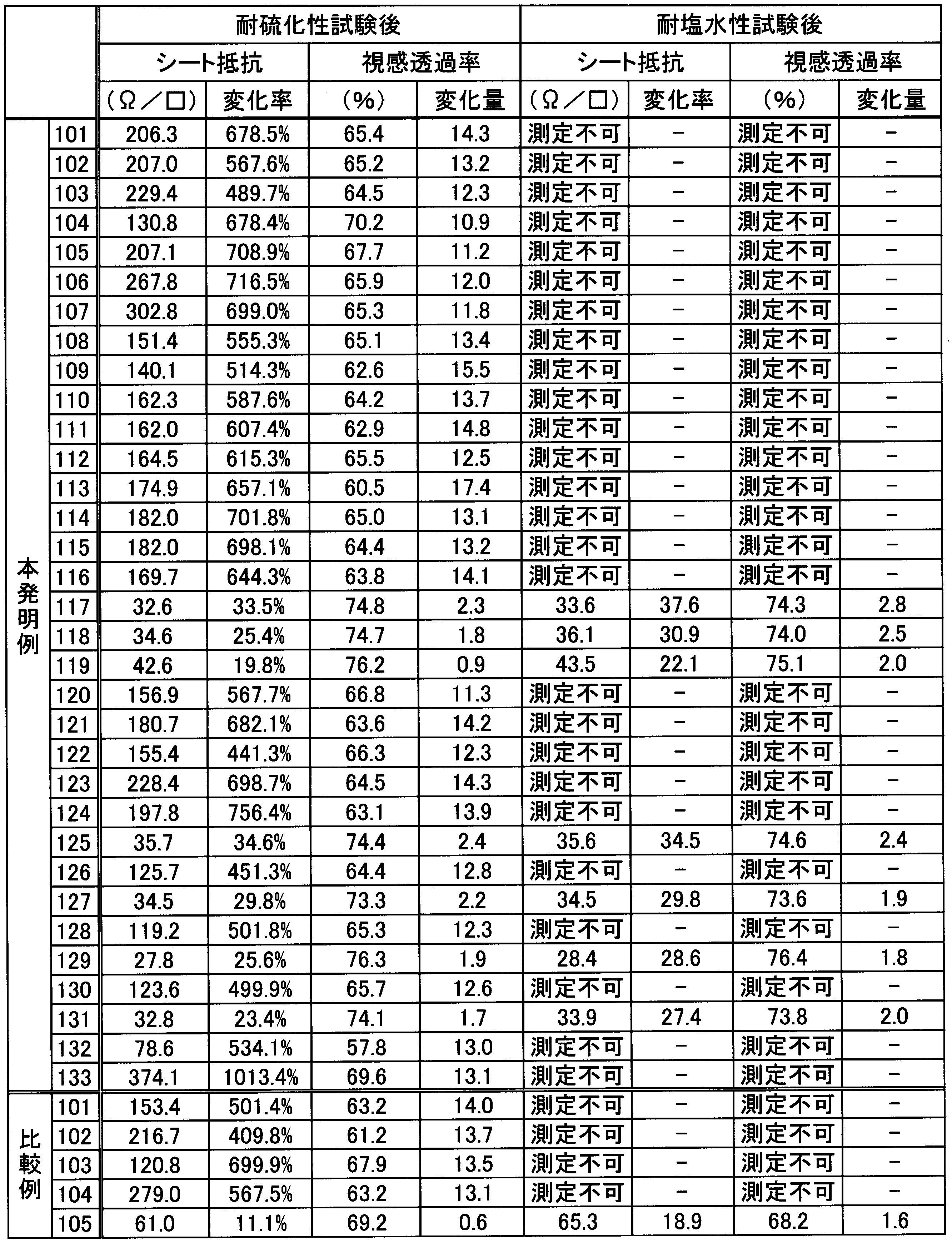
- the Ag alloy sputtering targets of Invention Examples 17 to 19, 25, 27, 29, and 31 containing Ti are excellent in sulfidation resistance and salt water resistance.
- an Ag alloy film excellent in electrical characteristics, optical characteristics, and environmental resistance can be formed, and the occurrence of abnormal discharge or the like during film formation can be suppressed.
- the Ag alloy film formed with the Ag alloy sputtering target according to the present invention has excellent conductivity (electrical characteristics), it is suitable for electronic devices such as organic EL devices.
Abstract
Description
本願は、2014年9月18日に日本に出願された特願2014-190278号、及び2015年9月7日に日本に出願された特願2015-175725号に基づき優先権を主張し、その内容をここに援用する。 The present invention relates to an Ag alloy sputtering target for forming an Ag alloy film applicable to, for example, a transparent conductive film for a display or a touch panel or a metal thin film of an optical functional film, a method for producing an Ag alloy sputtering target, and an Ag alloy film. And an Ag alloy film manufacturing method.
This application claims priority based on Japanese Patent Application No. 2014-190278 filed in Japan on September 18, 2014 and Japanese Patent Application No. 2015-175725 filed in Japan on September 7, 2015. The contents are incorporated herein.
特許文献3においては、Agに、白金、パラジウム、金、ロジウム、ルテニウム、イリジウム等の貴金属を添加したAg合金膜が提案されている。
また、特許文献4においては、Biを含有するとともにZn、Al、Ga、In、Si、Ge、Snから選ばれる少なくとも1種を含有するAg合金膜が提案されている。 Therefore, Patent Documents 3 and 4 propose Ag alloy films with improved environmental resistance.
Patent Document 3 proposes an Ag alloy film in which a noble metal such as platinum, palladium, gold, rhodium, ruthenium, or iridium is added to Ag.
Patent Document 4 proposes an Ag alloy film containing Bi and at least one selected from Zn, Al, Ga, In, Si, Ge, and Sn.
また、特許文献4に記載されたAg合金膜においては、吸収率が比較的高く、光学特性が不十分である。
特に、最近では、上述の透明導電膜及び光学機能性フィルムの金属薄膜には、さらなる視感透過率の向上が求められており、従来のAg合金膜では対応できなくなっていた。また、有機ELデバイス等の電子デバイスに用いられる透明導電膜には、優れた導電性(電気特性)も要求されている。 However, the Ag alloy film described in Patent Document 3 has a drawback in that the material cost is high because a noble metal is used as the additive element.
In addition, the Ag alloy film described in Patent Document 4 has a relatively high absorption rate and insufficient optical characteristics.
In particular, recently, further improvement in luminous transmittance has been demanded for the above-described transparent conductive film and metal thin film of the optical functional film, and conventional Ag alloy films have been unable to cope with it. In addition, a transparent conductive film used for an electronic device such as an organic EL device is also required to have excellent conductivity (electric properties).
この場合、前記不可避不純物のうちAgに対する固溶度が小さい元素であるNa,Si,V,Cr,Fe,Coの合計含有量を100質量ppm以下に制限しているので、これらの元素が結晶粒界に偏析することを抑制でき、スパッタ時における異常放電の発生を抑制することができる。
また、成膜されたAg合金膜においても、これらの元素が結晶粒界に偏析することが抑制されることになり、Ag合金膜の耐環境性が低下することを抑制できる。 Here, in the Ag alloy sputtering target according to the first aspect of the present invention, the total content of Na, Si, V, Cr, Fe, and Co among the inevitable impurities is preferably 100 mass ppm or less.
In this case, the total content of Na, Si, V, Cr, Fe, and Co, which are elements having a low solid solubility with respect to Ag among the inevitable impurities, is limited to 100 ppm by mass or less. Segregation at grain boundaries can be suppressed, and abnormal discharge during sputtering can be suppressed.
Also, in the formed Ag alloy film, segregation of these elements to the crystal grain boundaries is suppressed, and the environmental resistance of the Ag alloy film can be suppressed from decreasing.
この場合、Agに対する固溶度が小さい元素であるNa,Si,V,Cr,Fe,Coの各々の元素の含有量を30質量ppm以下に制限しているので、スパッタ時における異常放電の発生を確実に抑制することができる。また、成膜されたAg合金膜においても、耐環境性の低下を確実に抑制することができる。 In the Ag alloy sputtering target according to the first aspect of the present invention, the content of each of Na, Si, V, Cr, Fe, and Co among the inevitable impurities is 30 mass ppm or less. preferable.
In this case, the content of each element of Na, Si, V, Cr, Fe, and Co, which is an element having a low solid solubility with respect to Ag, is limited to 30 ppm by mass or less, so that abnormal discharge occurs during sputtering. Can be reliably suppressed. In addition, even in the formed Ag alloy film, it is possible to reliably suppress a decrease in environmental resistance.
この場合、平均結晶粒径が200μm以下とされているので、スパッタによってスパッタ面が消費された際に結晶方位によるスパッタレートの違いによって生じる凹凸を小さくすることができ、異常放電の発生を抑制することができる。
さらに、Cu,Sn又はこれらの金属間化合物からなる偏析部の粒径が1μm未満とされているので、長時間スパッタ時のスパッタレートおよび成膜したAg合金膜における成分組成を安定させることができる。なお、この偏析部は、組織中に存在しないことがさらに好ましい。 Furthermore, in the Ag alloy sputtering target according to the first aspect of the present invention, the average crystal grain size on the sputtering surface is 200 μm or less, and the grain size of the segregation part made of Cu, Sn or an intermetallic compound thereof is 1 μm. It is preferable to be less than.
In this case, since the average crystal grain size is 200 μm or less, the unevenness caused by the difference in the sputtering rate depending on the crystal orientation when the sputtering surface is consumed by sputtering can be reduced, and the occurrence of abnormal discharge is suppressed. be able to.
Furthermore, since the particle size of the segregation part made of Cu, Sn, or an intermetallic compound thereof is less than 1 μm, it is possible to stabilize the sputtering rate during long-time sputtering and the component composition in the deposited Ag alloy film. . In addition, it is more preferable that this segregation part does not exist in a structure | tissue.
この場合、Tiが0.1原子%以上添加されているので、成膜されたAg合金膜のケミカルに対する耐性を大幅に向上させることが可能となる。また、Tiの添加量が3.0原子%以下に制限されているので、成膜されたAg合金膜の光学特性及び電気特性の劣化を抑制することができる。 Moreover, in the Ag alloy sputtering target according to the first aspect of the present invention, it is preferable to further contain Ti in the range of 0.1 atomic% to 3.0 atomic%.
In this case, since 0.1 atomic% or more of Ti is added, the chemical resistance of the formed Ag alloy film can be greatly improved. Moreover, since the addition amount of Ti is limited to 3.0 atomic% or less, it is possible to suppress deterioration of optical characteristics and electrical characteristics of the formed Ag alloy film.
この構成のAg合金膜によれば、Snを0.1原子%以上3.0原子%以下、Cuを1.0原子%以上10.0原子%以下の範囲内で含有し、残部がAg及び不可避不純物からなる組成を有しているので、電気特性、耐環境性及び光学特性に優れることになり、透明導電膜や光学機能性フィルムの金属薄膜等として特に適している。 The Ag alloy film according to the third aspect of the present invention contains Sn in the range of 0.1 atomic% to 3.0 atomic% and Cu in the range of 1.0 atomic% to 10.0 atomic%, The remainder has a composition comprising Ag and inevitable impurities.
According to the Ag alloy film having this configuration, Sn is contained in the range of 0.1 atomic% to 3.0 atomic%, Cu is contained in the range of 1.0 atomic% to 10.0 atomic%, with the balance being Ag and Since it has a composition composed of inevitable impurities, it has excellent electrical characteristics, environmental resistance and optical characteristics, and is particularly suitable as a transparent conductive film, a metal thin film of an optical functional film, and the like.
この場合、視認性に優れることになり、各種ディスプレイやタッチパネルの透明導電膜や光学機能性フィルムの金属薄膜として好適に用いることができる。 In the Ag alloy film according to the third aspect of the present invention, the luminous transmittance is preferably 70% or more and the luminous absorption rate is 10% or less.
In this case, it will be excellent in visibility and can be used suitably as a transparent conductive film of various displays and touch panels, or a metal thin film of an optical functional film.
この場合、導電性に優れた透明導電膜として、各種ディスプレイやタッチパネルの電極膜や配線膜に適用することができる。 In the Ag alloy film according to the third aspect of the present invention, the sheet resistance value is preferably 40Ω / □ or less.
In this case, it can apply to the electrode film and wiring film of various displays and a touch panel as a transparent conductive film excellent in electroconductivity.
この場合、Ag合金膜の厚みが4nm以上とされているので、電気抵抗を確実に低くすることができ、導電性を確保できる。また、Ag合金膜の厚みが10nm以下とされているので、視感透過率を確実に向上させることができる。 In the Ag alloy film according to the third aspect of the present invention, the film thickness is preferably in the range of 4 nm to 10 nm.
In this case, since the thickness of the Ag alloy film is set to 4 nm or more, the electrical resistance can be reliably lowered and the conductivity can be ensured. Moreover, since the thickness of the Ag alloy film is 10 nm or less, the luminous transmittance can be improved with certainty.
この構成のAg合金膜の製造方法によれば、Cu及びSnを含有し、電気特性、耐環境性及び光学特性に優れたAg合金膜を成膜することができる。 The method for producing an Ag alloy film according to the fourth aspect of the present invention is characterized in that a film is formed by the Ag alloy sputtering target according to the first aspect described above.
According to the method for producing an Ag alloy film having this configuration, an Ag alloy film containing Cu and Sn and having excellent electrical characteristics, environmental resistance, and optical characteristics can be formed.
本実施形態であるAg合金スパッタリングターゲットは、Ag合金膜を成膜する際に用いられる。ここで、本実施形態であるAg合金膜は、例えばタッチパネルや太陽電池、有機ELデバイス等の電子デバイスの透明導電膜、光学機能性フィルムの金属薄膜として使用される。 Below, the Ag alloy sputtering target and Ag alloy film which are one Embodiment of this invention are demonstrated.
The Ag alloy sputtering target according to the present embodiment is used when an Ag alloy film is formed. Here, the Ag alloy film according to the present embodiment is used as a transparent conductive film of an electronic device such as a touch panel, a solar battery, or an organic EL device, and a metal thin film of an optical functional film.
本実施形態であるAg合金スパッタリングターゲットは、Snを0.1原子%以上3.0原子%以下、Cuを1.0原子%以上10.0原子%以下の範囲内で含有し、残部がAg及び不可避不純物とされた組成のAg合金で構成されている。
また、本実施形態では、前記不可避不純物のうちNa,Si,V,Cr,Fe,Coの合計含有量が100質量ppm以下とされている。また、前記不可避不純物のうちNa,Si,V,Cr,Fe,Coの各々の含有量が30質量ppm以下とされている。さらに、必要に応じて、Tiを0.1原子%以上3.0原子%以下の範囲内で含有していてもよい。 <Ag alloy sputtering target>
The Ag alloy sputtering target according to the present embodiment contains Sn in the range of 0.1 atomic% to 3.0 atomic%, Cu in the range of 1.0 atomic% to 10.0 atomic%, with the balance being Ag. And an Ag alloy having a composition of inevitable impurities.
In the present embodiment, the total content of Na, Si, V, Cr, Fe, and Co among the inevitable impurities is 100 mass ppm or less. Moreover, each content of Na, Si, V, Cr, Fe, and Co among the inevitable impurities is set to 30 ppm by mass or less. Furthermore, if necessary, Ti may be contained within a range of 0.1 atomic% to 3.0 atomic%.
以下に、本実施形態であるAg合金スパッタリングターゲットの組成、結晶組織を上述のように規定した理由について説明する。 In the Ag alloy sputtering target according to the present embodiment, the average crystal grain size on the sputtering surface is set to 200 μm or less, and the grain size of the segregation part made of Cu, Sn, or an intermetallic compound thereof is set to less than 1 μm. ing.
The reason why the composition and crystal structure of the Ag alloy sputtering target according to the present embodiment are defined as described above will be described below.
Snは、成膜したAg合金膜の耐環境性を向上させる作用効果を有する元素である。特に、熱湿環境下における光学特性の低下を効果的に抑制する作用効果を有する。
ここで、Ag合金スパッタリングターゲットにおけるSnの含有量が0.1原子%未満の場合には、上述の作用効果を十分に奏功せしめることができないおそれがある。一方、Ag合金スパッタリングターゲットにおけるSnの含有量が3.0原子%を超える場合には、成膜したAg合金膜の電気特性が低下するおそれがある。
このような理由から、本実施形態では、Ag合金スパッタリングターゲットにおけるSnの含有量を0.1原子%以上3.0原子%以下の範囲内に設定している。なお、上述の作用効果を確実に奏功せしめるためには、Ag合金スパッタリングターゲットにおけるSnの含有量の下限を0.4原子%以上、上限を2.0原子%以下とすることが好ましい。 (Sn: 0.1 atomic% to 3.0 atomic%)
Sn is an element having an effect of improving the environmental resistance of the formed Ag alloy film. In particular, it has the effect of effectively suppressing a decrease in optical properties in a hot and humid environment.
Here, when the content of Sn in the Ag alloy sputtering target is less than 0.1 atomic%, the above-described effects may not be sufficiently achieved. On the other hand, when the Sn content in the Ag alloy sputtering target exceeds 3.0 atomic%, the electrical characteristics of the formed Ag alloy film may be deteriorated.
For this reason, in the present embodiment, the Sn content in the Ag alloy sputtering target is set in the range of 0.1 atomic% to 3.0 atomic%. In order to ensure that the above-described effects are achieved, it is preferable that the lower limit of the Sn content in the Ag alloy sputtering target is 0.4 atomic% or more and the upper limit is 2.0 atomic% or less.
Cuは、成膜したAg合金膜の耐環境性を向上させる作用効果を有する元素である。特に、熱湿環境下における電気特性の低下を効果的に抑制する作用効果を有する。また、熱湿環境下において、成膜したAg合金膜における斑点等の発生を抑制する作用効果を有する。
ここで、Ag合金スパッタリングターゲットにおけるCuの含有量が1.0原子%未満の場合には、上述の作用効果を十分に奏功せしめることができないおそれがある。一方、Ag合金スパッタリングターゲットにおけるCuの含有量が10.0原子%を超える場合には、成膜したAg合金膜の電気特性が低下するおそれがある。また、成膜したAg合金膜の吸収率が増加して光学特性が低下するおそれがある。
このような理由から、本実施形態では、Ag合金スパッタリングターゲットにおけるCuの含有量を1.0原子%以上10.0原子%以下の範囲内に設定している。なお、上述の作用効果を確実に奏功せしめるためには、Ag合金スパッタリングターゲットにおけるCuの含有量の下限を2.0原子%以上、上限を8.0原子%以下とすることが好ましい。 (Cu: 1.0 atomic% or more and 10.0 atomic% or less)
Cu is an element having an effect of improving the environmental resistance of the formed Ag alloy film. In particular, it has the effect of effectively suppressing a decrease in electrical characteristics in a hot and humid environment. Moreover, it has the effect which suppresses generation | occurrence | production of the spot etc. in the Ag alloy film formed into a film in a hot-humid environment.
Here, when the content of Cu in the Ag alloy sputtering target is less than 1.0 atomic%, the above-described effects may not be sufficiently achieved. On the other hand, when the Cu content in the Ag alloy sputtering target exceeds 10.0 atomic%, the electrical characteristics of the formed Ag alloy film may be deteriorated. Further, the absorptance of the formed Ag alloy film may increase and the optical characteristics may deteriorate.
For this reason, in this embodiment, the Cu content in the Ag alloy sputtering target is set in the range of 1.0 atomic% or more and 10.0 atomic% or less. In order to ensure that the above-described effects are achieved, it is preferable that the lower limit of the Cu content in the Ag alloy sputtering target is 2.0 atomic% or more and the upper limit is 8.0 atomic% or less.
不可避不純物のうちNa,Si,V,Cr,Fe,Coといった元素は、Agに対する固溶度が小さいため、Ag合金スパッタリングターゲットの結晶粒界に偏析し、酸素と反応して酸化物が形成される。Ag合金スパッタリングターゲット中に酸化物が存在することにより、スパッタ中に異常放電及びスプラッシュが発生するおそれがある。また、Na,Si,V,Cr,Fe,Coといった元素は、成膜したAg合金膜においても結晶粒界に偏析しやすく、熱湿環境下において、これらの元素が酸化してAg合金膜の結晶性が低下し、耐環境性が低下するおそれがある。
このような理由から、本実施形態では、Ag合金スパッタリングターゲットにおいて、不可避不純物のうちNa,Si,V,Cr,Fe,Coの合計含有量を100質量ppm以下に制限している。また、よりいっそう、異常放電回数を抑制するために、本実施形態では、不可避不純物のうちNa,Si,V,Cr,Fe,Coの各々の含有量を30質量ppm以下に制限している。なお、不可避不純物のうちNa,Si,V,Cr,Fe,Coといった元素の合計含有量を20質量ppm以下とすることが好ましい。さらに、不可避不純物のうちNa,Si,V,Cr,Fe,Coといった元素の各々の含有量は10質量ppm以下とすることが好ましい。 (Na, Si, V, Cr, Fe, Co: total content is 100 mass ppm or less, each content is 30 mass ppm or less)
Among the inevitable impurities, elements such as Na, Si, V, Cr, Fe, and Co have a low solid solubility with respect to Ag, and therefore segregate at the grain boundaries of the Ag alloy sputtering target and react with oxygen to form oxides. The Due to the presence of oxide in the Ag alloy sputtering target, abnormal discharge and splash may occur during sputtering. In addition, elements such as Na, Si, V, Cr, Fe, and Co are easily segregated at the crystal grain boundaries even in the formed Ag alloy film, and these elements are oxidized in a hot and humid environment to form the Ag alloy film. There is a possibility that the crystallinity is lowered and the environmental resistance is lowered.
For this reason, in this embodiment, in the Ag alloy sputtering target, the total content of Na, Si, V, Cr, Fe, and Co among the inevitable impurities is limited to 100 mass ppm or less. Further, in order to further reduce the number of abnormal discharges, in this embodiment, the contents of Na, Si, V, Cr, Fe, and Co among unavoidable impurities are limited to 30 ppm by mass or less. Of the inevitable impurities, the total content of elements such as Na, Si, V, Cr, Fe, and Co is preferably 20 ppm by mass or less. Furthermore, it is preferable that the content of each element such as Na, Si, V, Cr, Fe, and Co among unavoidable impurities is 10 ppm by mass or less.
Tiを添加することにより、ケミカルに対する耐性が向上する。具体的には、成膜されたAg合金膜の耐硫黄性及び耐塩素性を向上させることが可能となる。
ここで、Tiの含有量が0.1原子%未満の場合には、上述の作用効果を十分に奏功せしめることができないおそれがある。一方、Tiの含有量が3.0原子%を超える場合には、成膜されたAg合金膜の光学特性及び電気特性の劣化するおそれがある。
このような理由から、本実施形態では、Tiを添加する場合にはTiの含有量を0.1原子%以上3.0原子%以下の範囲内に設定している。 (Ti: 0.1 atomic% to 3.0 atomic%)
Addition of Ti improves resistance to chemicals. Specifically, it becomes possible to improve the sulfur resistance and chlorine resistance of the formed Ag alloy film.
Here, when the Ti content is less than 0.1 atomic%, the above-described effects may not be sufficiently achieved. On the other hand, when the Ti content exceeds 3.0 atomic%, the optical characteristics and electrical characteristics of the formed Ag alloy film may be deteriorated.
For this reason, in the present embodiment, when Ti is added, the Ti content is set within a range of 0.1 atomic% to 3.0 atomic%.
スパッタレートは、結晶方位によって異なることから、スパッタが進行するとスパッタ面に、上述のスパッタレートの違いに起因して結晶粒に応じた凹凸が生じる。ここで、スパッタ面における平均結晶粒径が200μmを超えると、スパッタ面に生じる凹凸が大きくなり、凸部に電荷が集中して異常放電が発生しやすくなる。
このような理由から、本実施形態のAg合金スパッタリングターゲットにおいては、スパッタ面における平均結晶粒径を200μm以下に規定している。
なお、スパッタが進行した際のスパッタ面の凹凸を抑えて異常放電を確実に抑制するためには、スパッタ面における平均結晶粒径を150μm以下とすることが好ましく、80μm以下とすることがさらに好ましい。なお、平均結晶粒径の下限値は特に限定されないが、好ましくは30μm、より好ましくは50μmである。 (Average crystal grain size on the sputtering surface: 200 μm or less)
Since the sputtering rate varies depending on the crystal orientation, when the sputtering progresses, irregularities corresponding to the crystal grains are generated on the sputtering surface due to the above-described difference in the sputtering rate. Here, when the average crystal grain size on the sputter surface exceeds 200 μm, the unevenness generated on the sputter surface becomes large, and charges are concentrated on the convex portion, so that abnormal discharge is likely to occur.
For these reasons, in the Ag alloy sputtering target of the present embodiment, the average crystal grain size on the sputtering surface is regulated to 200 μm or less.
In addition, in order to suppress irregularities on the sputter surface when the sputtering progresses and to reliably suppress abnormal discharge, the average crystal grain size on the sputter surface is preferably 150 μm or less, and more preferably 80 μm or less. . The lower limit value of the average crystal grain size is not particularly limited, but is preferably 30 μm, more preferably 50 μm.
Snを0.1原子%以上3.0原子%以下、Cuを1.0原子%以上10.0原子%以下の範囲内で含有し、残部がAg及び不可避不純物からなる組成を有するAg合金スパッタリングターゲットにおいては、Cu,Snまたはこれらの金属間化合物からなる偏析部が存在することがある。ここで、上述の偏析部の粒径が1μm以上であると、長時間スパッタ時のスパッタレートが不安定となったり、成膜したAg合金膜の組成ばらつきが生じたりするおそれがある。
このような理由から、本実施形態のAg合金スパッタリングターゲットにおいては、Cu,Sn又はこれらの金属間化合物からなる偏析部の粒径を1μm未満に規定している。
なお、長時間スパッタ時のスパッタレートを確実に安定させるとともに、成膜したAg合金膜の組成ばらつきを確実に抑制するためには、Cu,Sn又はこれらの金属間化合物からなる偏析部が組織中に存在しないことがより好ましい。 (Particle size of segregation part made of Cu, Sn or an intermetallic compound thereof: less than 1 μm)
Ag alloy sputtering containing Sn in a range of 0.1 atomic% to 3.0 atomic%, Cu in a range of 1.0 atomic% to 10.0 atomic%, with the balance consisting of Ag and inevitable impurities In the target, there may be a segregation part made of Cu, Sn or an intermetallic compound thereof. Here, if the particle size of the segregation part is 1 μm or more, the sputtering rate during long-time sputtering may become unstable, or the composition variation of the deposited Ag alloy film may occur.
For these reasons, in the Ag alloy sputtering target of the present embodiment, the particle size of the segregated portion made of Cu, Sn, or an intermetallic compound thereof is specified to be less than 1 μm.
In order to reliably stabilize the sputtering rate during long-time sputtering and to reliably suppress the composition variation of the formed Ag alloy film, a segregated portion made of Cu, Sn, or an intermetallic compound thereof is included in the structure. More preferably not present in
次に、本実施形態に係るAg合金スパッタリングターゲットの製造方法について説明する。
まず、溶解原料として、純度99.9質量%以上のAgと純度99.9質量%以上のCu及びSnを準備する。なお、Tiを添加する場合には、純度99.9質量%以上のTiを準備する。
ここで、不可避不純物のうちNa,Si,V,Cr,Fe,Coの含有量を確実に低減するために、Ag原料に含まれるこれらの元素をICP分析等によって分析し、選別して使用する。なお、不可避不純物のうちNa,Si,V,Cr,Fe,Coの含有量を確実に低減するためには、Ag原料を硝酸又は硫酸等で浸出した後、所定のAg濃度の電解液を用いて電解精錬することが好ましい。 <Method for producing Ag alloy sputtering target>
Next, the manufacturing method of the Ag alloy sputtering target according to this embodiment will be described.
First, Ag having a purity of 99.9% by mass or more and Cu and Sn having a purity of 99.9% by mass or more are prepared as melting raw materials. In addition, when adding Ti, Ti with a purity of 99.9 mass% or more is prepared.
Here, in order to reliably reduce the contents of Na, Si, V, Cr, Fe, and Co among inevitable impurities, these elements contained in the Ag raw material are analyzed by ICP analysis or the like, selected and used. . In order to reliably reduce the content of Na, Si, V, Cr, Fe, and Co among inevitable impurities, after leaching the Ag raw material with nitric acid or sulfuric acid, etc., an electrolytic solution having a predetermined Ag concentration is used. Electrolytic refining is preferable.
次に、圧延後に熱処理を行う(熱処理工程)。この熱処理工程における熱処理温度が650℃以上750℃以下の範囲内とされている。なお、この熱処理温度での保持時間は、60min以上180min以下の範囲内とすることが好ましい。 Next, cold rolling is performed on the obtained Ag alloy ingot (rolling step). The rolling rate in this rolling step is preferably in the range of 60% to 80%.
Next, heat treatment is performed after rolling (heat treatment step). The heat treatment temperature in this heat treatment step is in the range of 650 ° C. or higher and 750 ° C. or lower. The holding time at this heat treatment temperature is preferably in the range of 60 min to 180 min.
本実施形態であるAg合金膜は、上述した本実施形態であるAg合金スパッタリングターゲットを用いて成膜されたものであり、Ag合金スパッタリングターゲットと同様の成分組成を有している。
Ag合金膜の光学特性として、可視光域における視感透過率が70%以上、視感吸収率が10%以下とされている。
Ag合金膜の電気特性として、シート抵抗値が40Ω/□以下とされている。 <Ag alloy film>
The Ag alloy film according to the present embodiment is formed using the above-described Ag alloy sputtering target according to the present embodiment, and has the same component composition as the Ag alloy sputtering target.
As the optical characteristics of the Ag alloy film, the luminous transmittance in the visible light region is 70% or more and the luminous absorption is 10% or less.
As an electrical characteristic of the Ag alloy film, the sheet resistance value is set to 40Ω / □ or less.
ここで、Ag合金膜の膜厚が4nm未満の場合には、電気特性を維持することができなくなるおそれがある。また、膜が凝集しやすくなるため、耐環境性が低下するおそれがある。一方、Ag合金膜の膜厚が10nmを超える場合には、吸収率等の光学特性が低下してしまうおそれがある。
このような理由から、本実施形態では、Ag合金膜の膜厚を4nm以上10nm以下の範囲内に設定している。なお、Ag合金膜の膜厚の下限は6nm以上とすることが好ましく、Ag合金膜の膜厚の上限は8nm以下とすることが好ましい。 Moreover, in the Ag alloy film which is this embodiment, the film thickness is in the range of 4 nm or more and 10 nm or less.
Here, when the thickness of the Ag alloy film is less than 4 nm, there is a possibility that the electrical characteristics cannot be maintained. Moreover, since the film tends to aggregate, the environmental resistance may be reduced. On the other hand, when the film thickness of the Ag alloy film exceeds 10 nm, the optical characteristics such as the absorptance may be deteriorated.
For this reason, in the present embodiment, the thickness of the Ag alloy film is set in the range of 4 nm to 10 nm. Note that the lower limit of the thickness of the Ag alloy film is preferably 6 nm or more, and the upper limit of the thickness of the Ag alloy film is preferably 8 nm or less.
成膜する基板としては、ガラス板又は箔、金属板又は箔、樹脂板又は樹脂フィルム等を用いることができる。また、成膜時の基板の配置については、静止対向方式やインライン方式等を採用することができる。 When forming an Ag alloy film according to this embodiment, it is preferable to apply a magnetron sputtering method, and as a power source, a direct current (DC) power source, a high frequency (RF) power source, a medium frequency (MF) power source, an alternating current (AC) ) Any power source can be selected.
As a substrate for film formation, a glass plate or foil, a metal plate or foil, a resin plate, a resin film, or the like can be used. In addition, a stationary facing method, an in-line method, or the like can be adopted for the arrangement of the substrate during film formation.
また、成膜したAg合金膜においても、これらの元素が結晶粒界に偏析することが抑制されることになり、Ag合金膜の耐環境性が低下することを抑制できる。 Furthermore, according to the Ag alloy sputtering target of the present embodiment, the total content of Na, Si, V, Cr, Fe, and Co, which is an element having a low solid solubility with respect to Ag among the inevitable impurities, is 100 mass ppm or less. Therefore, these elements can be prevented from segregating at the crystal grain boundaries to form oxides, and abnormal discharge and splash during sputtering can be suppressed.
Also, in the formed Ag alloy film, segregation of these elements to the crystal grain boundaries is suppressed, and the environmental resistance of the Ag alloy film can be suppressed from decreasing.
具体的には、光学特性として、視感透過率が70%以上、視感吸収率が10%以下とされているので、視認性に優れた透過膜として、本実施形態であるAg合金膜を用いることができる。
また、電気特性として、シート抵抗が40Ω/□以下とされているので、導電性に優れた導電膜として、本実施形態であるAg合金膜を用いることができる。 The Ag alloy film according to this embodiment is formed by the above-described Ag alloy sputtering target according to this embodiment and has the same component composition as the Ag alloy sputtering target according to this embodiment. It is excellent in properties, environmental resistance and optical properties, and is particularly suitable as a transparent conductive film, a metal thin film of an optical functional film, or the like.
Specifically, as the optical characteristics, the luminous transmittance is 70% or more and the luminous absorption is 10% or less. Therefore, the Ag alloy film according to the present embodiment is used as a permeable film having excellent visibility. Can be used.
Further, since the sheet resistance is 40Ω / □ or less as electrical characteristics, the Ag alloy film according to the present embodiment can be used as the conductive film having excellent conductivity.
例えば、本実施形態では、例えばタッチパネルや太陽電池、有機ELデバイス等の電子デバイスの透明導電膜、光学機能性フィルムの金属薄膜として使用されるものとして説明したが、これに限定されることはなく、その他の用途に用いてもよい。
また、Ag合金膜の膜厚については、本実施形態に限定されることはなく、使用用途に応じて適宜変更してもよい。 As mentioned above, although embodiment of this invention was described, this invention is not limited to this, It can change suitably in the range which does not deviate from the technical idea of the invention.
For example, in this embodiment, although demonstrated as what is used as a transparent conductive film of electronic devices, such as a touch panel, a solar cell, an organic EL device, and a metal thin film of an optical functional film, for example, it is not limited to this. It may be used for other purposes.
Further, the film thickness of the Ag alloy film is not limited to this embodiment, and may be appropriately changed according to the intended use.
まず、溶解原料として、純度99.9質量%以上のAgと、純度99.9質量%以上のCu,Sn,Tiを準備した。ここで、各不純物の含有量を低減させるために、Ag原料を硝酸又は硫酸で浸出した後、所定のAg濃度の電解液を用いて電解精製する方法を採用した。この精製方法でこれらの不純物が低減されたAg原料について、ICP法による不純物分析を実施し、Na、Si、V、Cr、Fe及びCoの濃度(含有量)の合計量が100ppm以下かつ各々の元素の濃度が30ppmであるAg原料を、スパッタリングターゲットの製造原料とした。 <Sputtering target for forming Ag alloy film>
First, Ag having a purity of 99.9% by mass or more and Cu, Sn, Ti having a purity of 99.9% by mass or more were prepared as melting raw materials. Here, in order to reduce the content of each impurity, a method was adopted in which an Ag raw material was leached with nitric acid or sulfuric acid and then subjected to electrolytic purification using an electrolytic solution having a predetermined Ag concentration. Impurity analysis by the ICP method is performed on the Ag raw material in which these impurities are reduced by this purification method, and the total amount (content) of Na, Si, V, Cr, Fe and Co is 100 ppm or less and each An Ag raw material having an element concentration of 30 ppm was used as a raw material for producing a sputtering target.
その後、大気中において、表2示す温度で1時間保持の熱処理を実施した。そして、機械加工を実施することにより、直径152.4mm、厚さ6mm寸法を有するAg合金スパッタリングターゲットを作製した。
なお、本発明例8~16のAg合金スパッタリングターゲットにおいては、溶解時にNa、Si、V、Cr、Fe、Coの各元素を意図的に適量添加した。また、本発明例20~23、30、31のAg合金スパッタリングターゲットにおいては、Ag合金の電解精製及び選別を実施しなかったAg原料を用いた。 Subsequently, the obtained Ag alloy ingot was cold-rolled at a reduction rate of 70%.
Thereafter, heat treatment was performed in the atmosphere for 1 hour at the temperature shown in Table 2. Then, by performing machining, an Ag alloy sputtering target having a diameter of 152.4 mm and a thickness of 6 mm was produced.
In the Ag alloy sputtering targets of Invention Examples 8 to 16, appropriate amounts of Na, Si, V, Cr, Fe, and Co were intentionally added during melting. Further, in the Ag alloy sputtering targets of Invention Examples 20 to 23, 30, and 31, Ag raw materials that were not subjected to electrolytic purification and selection of Ag alloys were used.
鋳造後のAg合金インゴットより分析用サンプルを採取し、そのサンプルをICP発光分光分析法により分析した。分析結果を表1に示す。 (Composition analysis)
A sample for analysis was collected from the cast Ag alloy ingot, and the sample was analyzed by ICP emission spectroscopy. The analysis results are shown in Table 1.
得られたAg合金スパッタリングターゲットのスパッタ面をその中心を通る線分で8等分に区分し、各部の中央部から試料片を採取した。各試料片のスパッタ面側を研磨する。#180~#4000の耐水紙で研磨をした後、3μm~1μmの砥粒でバフ研磨を行う。
次に、光学顕微鏡で粒界が見える程度にエッチングする。ここで、エッチング液には、過酸化水素水とアンモニア水との混合液を用い、室温で1~2秒間浸漬し、粒界を現出させる。次に、各試料について、光学顕微鏡で倍率30倍の写真を撮影した。
各写真において、60mmの線分を、格子状に20mm間隔で縦横に合計4本引き、それぞれの直線で切断された結晶粒の数を数えた。線分の端の結晶粒は、0.5個とカウントした。平均切片長さ:L(μm)を、L=60000/(M・N)(ここで、Mは実倍率、Nは切断された結晶粒数の平均値である)で求めた。求めた平均切片長さ:L(μm)から、試料の平均粒径:d(μm)を、d=(3/2)・Lで算出した。評価結果を表2に示す。 (Crystal grain size)
The sputtering surface of the obtained Ag alloy sputtering target was divided into 8 equal parts by a line segment passing through the center thereof, and sample pieces were collected from the central part of each part. The sputter surface side of each sample piece is polished. After polishing with # 180 to # 4000 water-resistant paper, buffing is performed with abrasive grains of 3 μm to 1 μm.
Next, it etches to such an extent that a grain boundary can be seen with an optical microscope. Here, a mixed liquid of hydrogen peroxide water and ammonia water is used as an etchant, and the mixture is immersed for 1 to 2 seconds at room temperature to reveal grain boundaries. Next, a photograph with a magnification of 30 times was taken with an optical microscope for each sample.
In each photograph, a total of four 60 mm line segments were drawn vertically and horizontally at intervals of 20 mm in a lattice shape, and the number of crystal grains cut along each straight line was counted. The number of crystal grains at the end of the line segment was counted as 0.5. Average section length: L (μm) was determined by L = 60000 / (M · N) (where M is an actual magnification and N is an average value of the number of crystal grains cut). From the obtained average section length: L (μm), the average particle diameter of the sample: d (μm) was calculated by d = (3/2) · L. The evaluation results are shown in Table 2.
結晶粒径の測定時と同様の方法で試料片を用意し、光学顕微鏡を用いて、倍率1500倍で写真撮影し、粒径1μm以上の偏析部の有無を確認した。評価結果を表2に示す。
なお、図1に偏析部の観察結果の一例を示す。図1(a)が本発明例1のAg合金スパッタリングターゲット、(b)が本発明例26のAg合金スパッタリングターゲットの観察結果である。本発明例1のAg合金スパッタリングターゲットにおいては、偏析部が黒点として観察される。 (Presence / absence of segregation part having a particle size of 1 μm or more)
A sample piece was prepared in the same manner as the measurement of the crystal grain size, and was photographed with an optical microscope at a magnification of 1500 times to confirm the presence or absence of a segregation part having a grain size of 1 μm or more. The evaluation results are shown in Table 2.
FIG. 1 shows an example of the observation result of the segregation part. FIG. 1A shows the observation results of the Ag alloy sputtering target of Invention Example 1, and FIG. 1B shows the observation results of the Ag alloy sputtering target of Invention Example 26. In the Ag alloy sputtering target of Invention Example 1, the segregated portion is observed as a black spot.
上述の本発明例及び比較例のAg合金スパッタリングターゲットを、無酸素銅製のバッキングプレートにインジウム半田を用いて半田付けしてターゲット複合体を作製した。
通常のマグネトロンスパッタ装置に、上述のターゲット複合体を取り付け、5×10⁻⁵Paまで排気した後、Arガス圧:0.5Pa、投入電力:直流1000W、ターゲット基板間距離:70mmの条件でスパッタを実施した。スパッタ時の異常放電回数は、MKSインスツルメント社製DC電源(RPDG-50A)のアークカウント機能により、放電開始から1時間の異常放電回数として計測した。評価結果を表2に示す。 (Number of abnormal discharges at the beginning of use)
The above-described Ag alloy sputtering targets of the present invention and the comparative examples were soldered to an oxygen-free copper backing plate using indium solder to prepare a target composite.
After mounting the above-mentioned target composite on a normal magnetron sputtering apparatus and exhausting to 5 × 10 −5 Pa, sputtering is performed under the conditions of Ar gas pressure: 0.5 Pa, input power: DC 1000 W, and distance between target substrates: 70 mm. Carried out. The number of abnormal discharges during sputtering was measured as the number of abnormal discharges for one hour from the start of discharge using the arc count function of a DC power supply (RPDG-50A) manufactured by MKS Instruments. The evaluation results are shown in Table 2.
4時間の空スパッタと防着板の交換とを繰り返して、断続的に20時間スパッタすることによりターゲットを消耗させた。その後に更に、上述の条件でスパッタを行い、消耗(20時間のスパッタ)後の1時間に生じた異常放電の回数を測定した。評価結果を表2に示す。 (Number of abnormal discharge after long-time sputtering)
The target was consumed by intermittently sputtering for 20 hours by repeating the empty sputtering for 4 hours and replacing the deposition prevention plate. Thereafter, sputtering was performed under the above-described conditions, and the number of abnormal discharges that occurred in one hour after consumption (sputtering for 20 hours) was measured. The evaluation results are shown in Table 2.
使用初期においてスパッタレートを測定後、上記と同様に4時間の空スパッタと防着板の交換とを繰り返して、断続的に20時間スパッタすることによりターゲットを消耗させた。その後に更にスパッタを行い、スパッタレートの測定を行い、下記の式でスパッタレートの変化比を評価した。評価結果を表2に示す。
スパッタレートの変化比=長時間スパッタ後のレート/使用初期のレート (Change ratio of sputtering rate before and after long-time sputtering)
After the sputtering rate was measured in the initial stage of use, the target was consumed by intermittently sputtering for 20 hours by repeating the empty sputtering for 4 hours and replacing the deposition prevention plate in the same manner as described above. Thereafter, sputtering was further performed to measure the sputtering rate, and the change rate of the sputtering rate was evaluated by the following formula. The evaluation results are shown in Table 2.
Change ratio of sputtering rate = rate after long-time sputtering / initial rate of use
使用初期において成膜されたAg合金膜の組成を測定した。膜組成の測定方法としては、Ag合金膜を3000nm成膜し、その膜をICP分光分析法にて測定した。その後、上記と同様に4時間の空スパッタと防着板の交換とを繰り返して、断続的に20時間スパッタすることによりターゲットを消耗させた。その後に更にスパッタを行い、成膜されたAg合金膜の組成の測定を行い、下記の式で膜組成の変化率を評価した。評価結果を表2に示す。
膜組成の変化率(%)=(長時間スパッタ後の添加元素Aの組成/使用初期の添加元素Aの組成)×100
なお、添加元素Aは、各添加元素のうち最も変化率の大きいものとした。 (Change rate of film composition before and after long-time sputtering)
The composition of the Ag alloy film formed in the initial stage of use was measured. As a method for measuring the film composition, an Ag alloy film was formed to 3000 nm, and the film was measured by ICP spectroscopy. Thereafter, the sputtering was repeated for 4 hours in the same manner as described above and the deposition plate was replaced, and the target was consumed by intermittently sputtering for 20 hours. Thereafter, sputtering was further performed, the composition of the formed Ag alloy film was measured, and the rate of change of the film composition was evaluated by the following formula. The evaluation results are shown in Table 2.
Change rate of film composition (%) = (composition of additive element A after long-time sputtering / composition of additive element A at the beginning of use) × 100
Note that the additive element A has the highest rate of change among the additive elements.
上述の本発明例及び比較例のAg合金スパッタリングターゲットをスパッタ装置に装着し、下記の条件でAg合金膜を成膜した。
基板:洗浄済みガラス基板(コーニング社製イーグルXG 厚み0.7mm)
到達真空度:5×10⁻⁵Pa以下
使用ガス:Ar
ガス圧:0.5Pa
スパッタリング電力:直流200W
ターゲット/基板間距離:70mm <Ag alloy film>
The above-described Ag alloy sputtering targets of the present invention and the comparative example were mounted on a sputtering apparatus, and an Ag alloy film was formed under the following conditions.
Substrate: Washed glass substrate (Corning Eagle XG thickness 0.7mm)
Ultimate vacuum: 5 × 10 −5 Pa or less Gas used: Ar
Gas pressure: 0.5Pa
Sputtering power: DC 200W
Target / substrate distance: 70 mm
クロスセクションポリッシャ(CP)によって観察試料を作製し、透過電子顕微鏡(TEM)によってAg合金膜の断面を観察し、Ag合金膜の膜厚を算出した。膜構造を表3に示す。 (Measurement of film thickness)
An observation sample was prepared with a cross section polisher (CP), a cross section of the Ag alloy film was observed with a transmission electron microscope (TEM), and the film thickness of the Ag alloy film was calculated. Table 3 shows the film structure.
成膜したAg合金膜について、温度85℃、湿度85%の恒温恒湿槽中に250時間放置した。 (Constant temperature and humidity test)
The formed Ag alloy film was left for 250 hours in a constant temperature and humidity chamber having a temperature of 85 ° C. and a humidity of 85%.
成膜後のAg合金膜のシート抵抗値RS0及び恒温恒湿試験後のAg合金膜のシート抵抗値RS1を、三菱化学製抵抗測定器ロレスタGPによる四探針法により測定した。また、恒温恒湿試験前後の変化率(%)を以下の式で算出した。測定結果を表3及び表4に示す。
変化率(%)=(RS1-RS0)/RS0×100 (Sheet resistance value)
The sheet resistance value R S0 of the Ag alloy film after film formation and the sheet resistance value R S1 of the Ag alloy film after the constant temperature and humidity test were measured by a four-probe method using a resistance measuring instrument Loresta GP manufactured by Mitsubishi Chemical. Further, the change rate (%) before and after the constant temperature and humidity test was calculated by the following formula. The measurement results are shown in Tables 3 and 4.
Rate of change (%) = (R S1 −R S0 ) / R S0 × 100
Ag合金膜の視感透過率の測定は、分光光度計(株式会社日立ハイテクノロジーズ製U-4100)を用いて行い、薄膜を形成していない基板の透過率を100として、膜の透過率の相対評価を行った。透過率スペクトル%Tを波長780~380nmの範囲で測定し、このスペクトルから色彩計算プログラム(JIS Z 8722に準拠)を用いて、光源D65及び視野2°におけるXYZ表色系のY値を算出し、計算された値を視感透過率とした。
成膜後のAg合金膜の視感透過率T0及び恒温恒湿試験後のAg合金膜の視感透過率T1を上述のように測定した。また、恒温恒湿試験前後の変化量T1-T0を算出した。測定結果を表3及び表4に示す。 (Visibility transmittance)
The luminous transmittance of the Ag alloy film was measured using a spectrophotometer (U-4100, manufactured by Hitachi High-Technologies Corporation). The transmittance of the film was measured with the transmittance of the substrate on which the thin film was not formed being 100. Relative evaluation was performed. The transmittance spectrum% T is measured in the wavelength range of 780 to 380 nm, and the Y value of the XYZ color system at the light source D65 and the visual field of 2 ° is calculated from this spectrum using a color calculation program (conforming to JIS Z8722). The calculated value was defined as luminous transmittance.
The luminous transmittance T 0 of the Ag alloy film after film formation and the luminous transmittance T 1 of the Ag alloy film after the constant temperature and humidity test were measured as described above. Further, the amount of change T 1 -T 0 before and after the constant temperature and humidity test was calculated. The measurement results are shown in Tables 3 and 4.
Ag合金膜の視感吸収率は、上記分光光度で測定した透過率スペクトル%Tと、反射率スペクトル%Rを波長780~380nmの範囲で測定し、これらのスペクトルから吸収率スペクトル%Aを以下の式で算出した。
%A=100-(%T+%R)
このスペクトルから色彩計算プログラム(JIS Z 8722に準拠)を用いて、光源D65及び視野2°におけるXYZ表色系のY値を算出し、計算された値を視感吸収率とした。
成膜後のAg合金膜の視感吸収率A0及び恒温恒湿試験後のAg合金膜の視感吸収率A1を上述のように測定した。また、恒温恒湿試験前後の変化量A1-A0を算出した。測定結果を表3及び表4に示す。 (Visibility absorption rate)
The luminous absorptance of the Ag alloy film was determined by measuring the transmittance spectrum% T and the reflectance spectrum% R measured in the above spectrophotometer in the wavelength range of 780 to 380 nm. It was calculated by the following formula.
% A = 100-(% T +% R)
From this spectrum, a color calculation program (based on JIS Z 8722) was used to calculate the Y value of the XYZ color system at the light source D65 and the field of view of 2 °, and the calculated value was used as the luminous absorption rate.
The luminous absorption rate A 0 of the Ag alloy film after film formation and the luminous absorption rate A 1 of the Ag alloy film after the constant temperature and humidity test were measured as described above. Further, the amount of change A 1 -A 0 before and after the constant temperature and humidity test was calculated. The measurement results are shown in Tables 3 and 4.
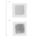
温度85℃、湿度85%の恒温恒湿層中に250時間放置したAg合金膜の外観を目視で観察した。図2の(a)に示すように、膜の表面に斑点状の変色が認められなかったAg合金膜を「A」、図2の(b)に示すように、膜の表面に斑点状の変色が認められたAg合金膜を「B」と評価した。評価結果を表4に示す。 (Appearance observation after constant temperature and humidity test)
The appearance of the Ag alloy film left in a constant temperature and humidity layer having a temperature of 85 ° C. and a humidity of 85% for 250 hours was visually observed. As shown in FIG. 2 (a), an Ag alloy film in which no spot-like discoloration was observed on the surface of the film was “A”, and as shown in FIG. 2 (b), the surface of the film was spotted. The Ag alloy film in which discoloration was observed was evaluated as “B”. The evaluation results are shown in Table 4.
成膜サンプルに対して、室温で0.01mass%の硫化ナトリウム水溶液中に30分浸漬し、水溶液から取り出して純水で十分に洗浄した後、乾燥空気を噴射して水分を取り除いた。これらの試料について、上述と同様にシート抵抗、透過率を測定し、透過率の変化分及びシート抵抗の変化率により耐硫化性の評価を行った。評価結果を表5に示す。 (Sulfuration resistance test)
The film formation sample was immersed in a 0.01 mass% sodium sulfide aqueous solution at room temperature for 30 minutes, taken out from the aqueous solution and thoroughly washed with pure water, and then dried air was sprayed to remove moisture. With respect to these samples, the sheet resistance and transmittance were measured in the same manner as described above, and the sulfidation resistance was evaluated based on the change in transmittance and the rate of change in sheet resistance. The evaluation results are shown in Table 5.
成膜サンプルに対して、室温で、5%NaCl水溶液中に24時間浸漬し、水溶液から取り出して純水で十分に洗浄した後、乾燥空気を噴射して水分を取り除いた。これらの試料について、上述と同様にシート抵抗、透過率を測定し、透過率変化分及びシート抵抗の変化率により耐塩水性の評価を行った。評価結果を表5に示す。なお、表5においては、5%NaCl水溶液に浸漬後に膜が消失したものについては「測定不可」と表記した。 (Salt water resistance test)
The film formation sample was immersed in a 5% NaCl aqueous solution at room temperature for 24 hours, taken out from the aqueous solution and thoroughly washed with pure water, and then dried air was sprayed to remove moisture. About these samples, sheet resistance and the transmittance | permeability were measured similarly to the above, and salt water resistance was evaluated by the transmittance | permeability change part and the change rate of sheet resistance. The evaluation results are shown in Table 5. In Table 5, those in which the film disappeared after being immersed in a 5% NaCl aqueous solution were described as “not measurable”.

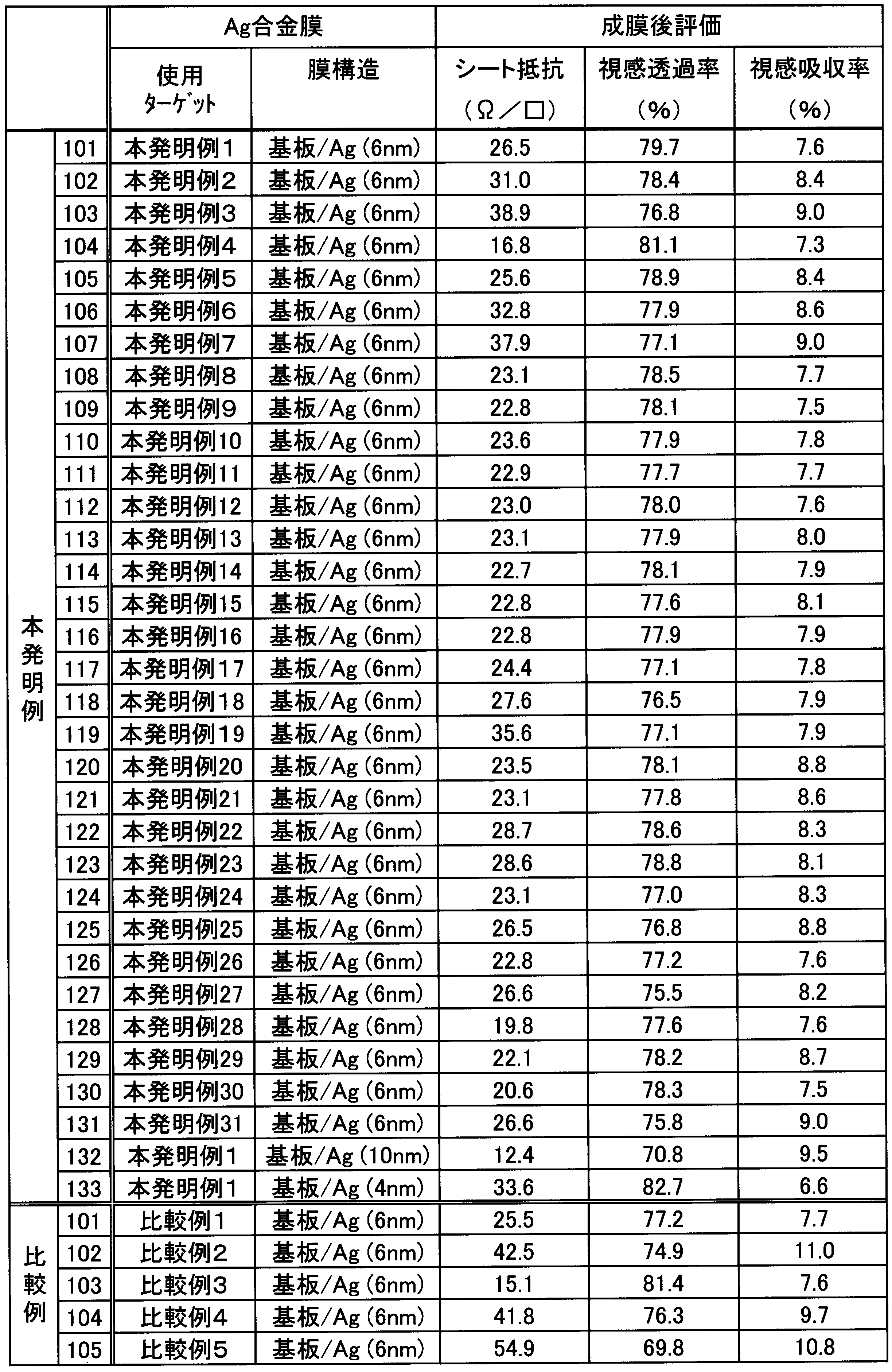
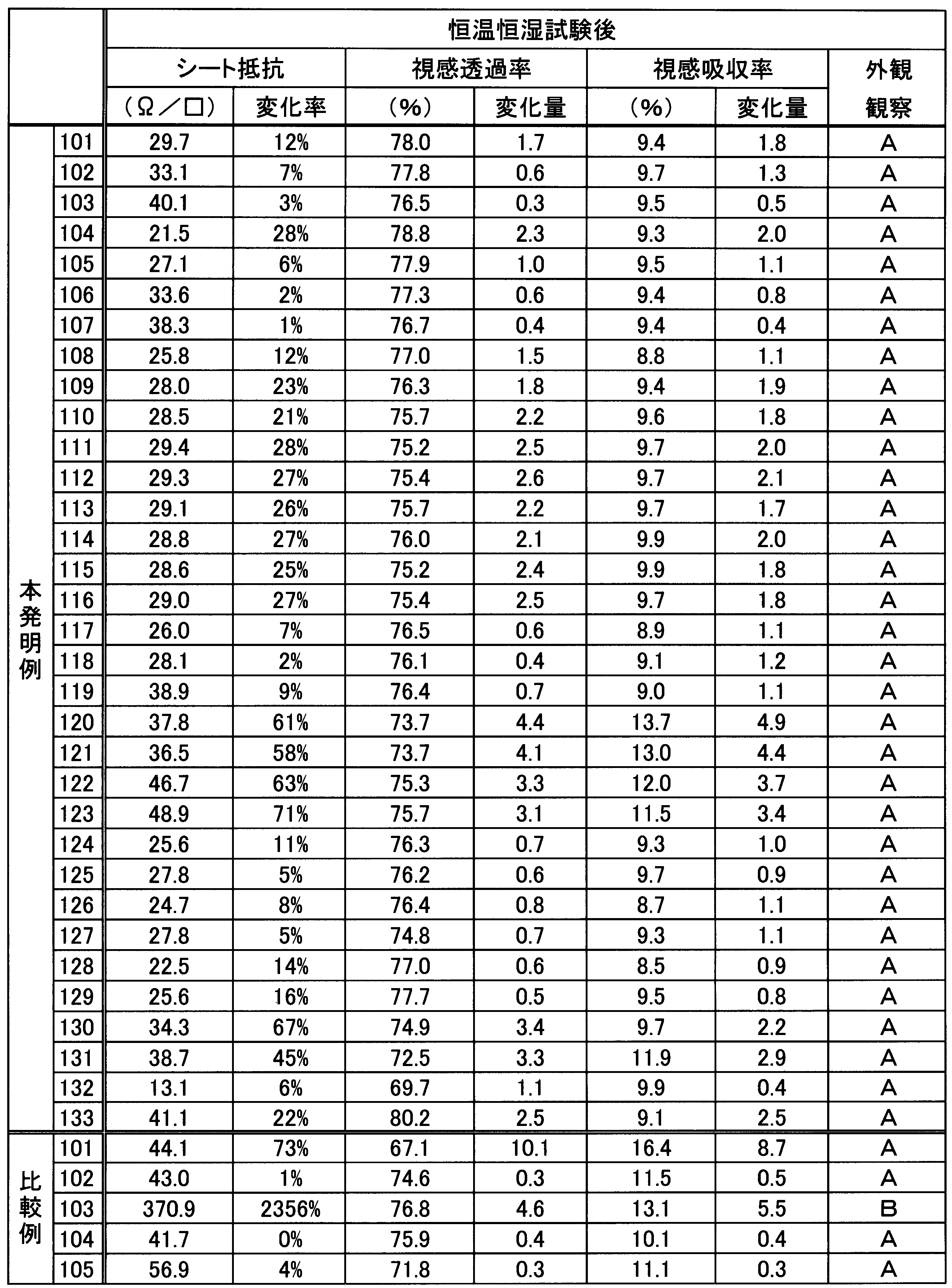
Snの含有量が本発明の範囲よりも多い比較例2のAg合金スパッタリングターゲットを用いて成膜された比較例102のAg合金膜においては、成膜後のシート抵抗、及び、視感吸収率が高く、電気特性、光学特性が不十分であった。 In the Ag alloy film of Comparative Example 101 formed using the Ag alloy sputtering target of Comparative Example 1 having a Sn content less than the range of the present invention, the luminous transmittance and luminous absorption after the constant temperature and humidity test The rate was greatly deteriorated and the environmental resistance was insufficient.
In the Ag alloy film of Comparative Example 102 formed using the Ag alloy sputtering target of Comparative Example 2 having a Sn content larger than the range of the present invention, the sheet resistance after film formation and the luminous absorption rate were increased. The electrical properties and optical properties were insufficient.
Cuの含有量が本発明の範囲よりも多い比較例4のAg合金スパッタリングターゲットを用いて成膜された比較例104のAg合金膜においては、成膜後のシート抵抗が高く、電気特性が不十分であった。 In the Ag alloy film of Comparative Example 103 formed using the Ag alloy sputtering target of Comparative Example 3 having a Cu content less than the range of the present invention, the sheet resistance is remarkably increased after the constant temperature and humidity test. Spots were formed on the surface, and the environmental resistance characteristics were insufficient.
In the Ag alloy film of Comparative Example 104 formed using the Ag alloy sputtering target of Comparative Example 4 in which the Cu content is larger than the range of the present invention, the sheet resistance after film formation is high and the electrical characteristics are poor. It was enough.
これに対して、本発明例のAg合金スパッタリングターゲットを用いて成膜されたAg合金膜においては、電気特性、光学特性及び耐環境特性のいずれも優れていた。 In the Ag alloy film of Comparative Example 105 formed using the Ag alloy sputtering target of Comparative Example 5 having a Ti content larger than the range of the present invention, the sheet resistance after film formation is high, and the visual sense The transmittance was low, and the electrical and optical properties were insufficient.
On the other hand, the Ag alloy film formed using the Ag alloy sputtering target of the present invention example was excellent in all of electric characteristics, optical characteristics, and environmental resistance characteristics.
また、本発明例11~16のAg合金スパッタリングターゲットにおいては、不純物元素のうちNa,Si,V,Cr,Fe,Coのいずれかの含有量が30質量ppmを超えており、やや異常放電回数が多かった。
これに対して、不純物元素のうちNa,Si,V,Cr,Fe,Coの合計含有量が100質量ppm以下であり、Na,Si,V,Cr,Fe,Coの各々の含有量も30質量ppm以下とされた他の本発明例のAg合金スパッタリングターゲットにおいては、異常放電回数が少なかった。 Next, in the Ag alloy sputtering targets of Invention Examples 20 to 23, 30, and 31, the total content of Na, Si, V, Cr, Fe, and Co among impurity elements exceeds 100 ppm by mass, There were many discharges.
In the Ag alloy sputtering targets of Invention Examples 11 to 16, the content of any one of the impurity elements, Na, Si, V, Cr, Fe, and Co, exceeds 30 mass ppm, and the number of abnormal discharges is somewhat There were many.
In contrast, the total content of Na, Si, V, Cr, Fe, and Co among impurity elements is 100 mass ppm or less, and the content of each of Na, Si, V, Cr, Fe, and Co is also 30. In the Ag alloy sputtering target of another example of the present invention having a mass ppm or less, the number of abnormal discharges was small.
これに対して、スパッタ面の平均結晶粒径が200μm以下とされた他の本発明例のAg合金スパッタリングターゲットにおいては、長時間スパッタ後においても異常放電回数が少なかった。 In addition, in the Ag alloy sputtering targets of Invention Examples 28 and 29 in which the average crystal grain size on the sputtering surface exceeded 200 μm, the number of abnormal discharges after long-time sputtering increased.
On the other hand, in other Ag alloy sputtering targets of the present invention in which the average crystal grain size of the sputtering surface was 200 μm or less, the number of abnormal discharges was small even after long-time sputtering.
これに対して、粒径1μm以上の偏析部が観察されなかった他の本発明例のAg合金スパッタリングターゲットにおいては、長時間スパッタ後のスパッタレートの変化比、膜組成の変化率が抑えられていた。 Further, in the Ag alloy sputtering targets of Examples 1 to 23 in which segregation portions having a particle diameter of 1 μm or more were observed, the change rate of the sputtering rate and the change rate of the film composition after long-time sputtering were relatively large.
On the other hand, in the Ag alloy sputtering target of another example of the present invention in which a segregation part having a particle size of 1 μm or more was not observed, the change rate of the sputtering rate after long-time sputtering and the change rate of the film composition were suppressed. It was.
Claims (11)
- Snを0.1原子%以上3.0原子%以下、Cuを1.0原子%以上10.0原子%以下の範囲内で含有し、残部がAg及び不可避不純物からなる組成を有することを特徴とするAg合金スパッタリングターゲット。 It contains Sn in a range of 0.1 atomic% to 3.0 atomic%, Cu in a range of 1.0 atomic% to 10.0 atomic%, and the balance is composed of Ag and inevitable impurities. An Ag alloy sputtering target.
- 前記不可避不純物のうちNa,Si,V,Cr,Fe,Coの合計含有量が100質量ppm以下であることを特徴とする請求項1に記載のAg合金スパッタリングターゲット。 The Ag alloy sputtering target according to claim 1, wherein a total content of Na, Si, V, Cr, Fe and Co among the inevitable impurities is 100 mass ppm or less.
- 前記不可避不純物のうちNa,Si,V,Cr,Fe,Coの各々の含有量が30質量ppm以下とされていることを特徴とする請求項1または請求項2に記載のAg合金スパッタリングターゲット。 3. The Ag alloy sputtering target according to claim 1, wherein the content of Na, Si, V, Cr, Fe, and Co among the inevitable impurities is 30 mass ppm or less.
- スパッタ面における平均結晶粒径が200μm以下とされ、さらに、Cu,Snまたはこれらの金属間化合物からなる偏析部の粒径が1μm未満とされていることを特徴とする請求項1から請求項3のいずれか一項に記載のAg合金スパッタリングターゲット。 The average crystal grain size on the sputtering surface is 200 μm or less, and the grain size of the segregation part made of Cu, Sn, or an intermetallic compound thereof is less than 1 μm. The Ag alloy sputtering target according to any one of the above.
- さらにTiを0.1原子%以上3.0原子%以下の範囲内で含有することを特徴とする請求項1から請求項4のいずれか一項に記載のAg合金スパッタリングターゲット。 Furthermore, Ti is contained within the range of 0.1 atomic% or more and 3.0 atomic% or less, Ag alloy sputtering target as described in any one of Claims 1-4 characterized by the above-mentioned.
- 請求項4に記載のAg合金スパッタリングターゲットの製造方法であって、
Ag合金インゴットを作製する溶解鋳造工程と、得られたAg合金インゴットに圧延を行う圧延工程と、圧延後に熱処理を行う熱処理工程と、を有し、
前記熱処理工程における熱処理温度が650℃以上750℃以下の範囲内とされていることを特徴とするAg合金スパッタリングターゲットの製造方法。 It is a manufacturing method of the Ag alloy sputtering target according to claim 4,
A melt casting step for producing an Ag alloy ingot, a rolling step for rolling the obtained Ag alloy ingot, and a heat treatment step for performing a heat treatment after rolling,
The method for producing an Ag alloy sputtering target, wherein a heat treatment temperature in the heat treatment step is in a range from 650 ° C. to 750 ° C. - Snを0.1原子%以上3.0原子%以下、Cuを1.0原子%以上10.0原子%以下の範囲内で含有し、残部がAg及び不可避不純物からなる組成を有することを特徴とするAg合金膜。 It contains Sn in a range of 0.1 atomic% to 3.0 atomic%, Cu in a range of 1.0 atomic% to 10.0 atomic%, and the balance is composed of Ag and inevitable impurities. An Ag alloy film.
- 視感透過率が70%以上、視感吸収率が10%以下であることを特徴とする請求項7に記載のAg合金膜。 The Ag alloy film according to claim 7, wherein the luminous transmittance is 70% or more and the luminous absorption is 10% or less.
- シート抵抗値が40Ω/□以下であることを特徴とする請求項7または請求項8に記載のAg合金膜。 The Ag alloy film according to claim 7 or 8, wherein the sheet resistance value is 40Ω / □ or less.
- 膜厚が4nm以上10nm以下の範囲内であることを特徴とする請求項7から請求項9のいずれか一項に記載のAg合金膜。 The Ag alloy film according to any one of claims 7 to 9, wherein the film thickness is within a range of 4 nm or more and 10 nm or less.
- 請求項1から請求項5のいずれか一項に記載されたAg合金スパッタリングターゲットによって成膜することを特徴とするAg合金膜の製造方法。 A method for producing an Ag alloy film, comprising forming a film using the Ag alloy sputtering target according to any one of claims 1 to 5.
Priority Applications (5)
| Application Number | Priority Date | Filing Date | Title |
|---|---|---|---|
| US15/502,019 US10060025B2 (en) | 2014-09-18 | 2015-09-15 | Ag alloy sputtering target, method of manufacturing Ag alloy sputtering target, Ag alloy film, and method of forming Ag alloy film |
| EP15842240.2A EP3196333B1 (en) | 2014-09-18 | 2015-09-15 | Ag alloy sputtering target and manufacturing method for ag alloy film |
| KR1020187009760A KR102046732B1 (en) | 2014-09-18 | 2015-09-15 | Ag ALLOY SPUTTERING TARGET, MANUFACTURING METHOD FOR Ag ALLOY SPUTTERING TARGET, Ag ALLOY FILM, AND MANUFACTURING METHOD FOR ALLOY FILM |
| CN201580042235.XA CN106574361B (en) | 2014-09-18 | 2015-09-15 | Ag alloy sputtering targets, the manufacture method of Ag alloy sputtering targets, the manufacture method of Ag alloy films and Ag alloy films |
| KR1020177007264A KR20170055969A (en) | 2014-09-18 | 2015-09-15 | Ag ALLOY SPUTTERING TARGET, MANUFACTURING METHOD FOR Ag ALLOY SPUTTERING TARGET, Ag ALLOY FILM, AND MANUFACTURING METHOD FOR ALLOY FILM |
Applications Claiming Priority (4)
| Application Number | Priority Date | Filing Date | Title |
|---|---|---|---|
| JP2014190278 | 2014-09-18 | ||
| JP2014-190278 | 2014-09-18 | ||
| JP2015175725A JP6172230B2 (en) | 2014-09-18 | 2015-09-07 | Ag alloy sputtering target, Ag alloy film, and method for producing Ag alloy film |
| JP2015-175725 | 2015-09-07 |
Publications (1)
| Publication Number | Publication Date |
|---|---|
| WO2016043183A1 true WO2016043183A1 (en) | 2016-03-24 |
Family
ID=55533220
Family Applications (1)
| Application Number | Title | Priority Date | Filing Date |
|---|---|---|---|
| PCT/JP2015/076124 WO2016043183A1 (en) | 2014-09-18 | 2015-09-15 | Ag ALLOY SPUTTERING TARGET, MANUFACTURING METHOD FOR Ag ALLOY SPUTTERING TARGET, Ag ALLOY FILM, AND MANUFACTURING METHOD FOR ALLOY FILM |
Country Status (1)
| Country | Link |
|---|---|
| WO (1) | WO2016043183A1 (en) |
Cited By (3)
| Publication number | Priority date | Publication date | Assignee | Title |
|---|---|---|---|---|
| CN106893990A (en) * | 2017-02-17 | 2017-06-27 | 南京东锐铂业有限公司 | The production technology of silver-colored sputtering target material component |
| CN112119179A (en) * | 2018-05-17 | 2020-12-22 | 三菱综合材料株式会社 | Laminated film and Ag alloy sputtering target |
| EP3862459A4 (en) * | 2018-10-03 | 2022-05-11 | Mitsubishi Materials Corporation | Multilayer film, and ag alloy sputtering target |
Citations (2)
| Publication number | Priority date | Publication date | Assignee | Title |
|---|---|---|---|---|
| JP2012207445A (en) * | 2011-03-30 | 2012-10-25 | Tokai Rubber Ind Ltd | Transparent rolling screen |
| JP2013216976A (en) * | 2012-04-04 | 2013-10-24 | Heraeus Materials Technology Gmbh & Co Kg | Flat or tubular sputtering target and manufacturing method therefor |
-
2015
- 2015-09-15 WO PCT/JP2015/076124 patent/WO2016043183A1/en active Application Filing
Patent Citations (2)
| Publication number | Priority date | Publication date | Assignee | Title |
|---|---|---|---|---|
| JP2012207445A (en) * | 2011-03-30 | 2012-10-25 | Tokai Rubber Ind Ltd | Transparent rolling screen |
| JP2013216976A (en) * | 2012-04-04 | 2013-10-24 | Heraeus Materials Technology Gmbh & Co Kg | Flat or tubular sputtering target and manufacturing method therefor |
Cited By (4)
| Publication number | Priority date | Publication date | Assignee | Title |
|---|---|---|---|---|
| CN106893990A (en) * | 2017-02-17 | 2017-06-27 | 南京东锐铂业有限公司 | The production technology of silver-colored sputtering target material component |
| CN106893990B (en) * | 2017-02-17 | 2019-02-01 | 南京东锐铂业有限公司 | The production technology of silver-colored sputtering target material component |
| CN112119179A (en) * | 2018-05-17 | 2020-12-22 | 三菱综合材料株式会社 | Laminated film and Ag alloy sputtering target |
| EP3862459A4 (en) * | 2018-10-03 | 2022-05-11 | Mitsubishi Materials Corporation | Multilayer film, and ag alloy sputtering target |
Similar Documents
| Publication | Publication Date | Title |
|---|---|---|
| JP6278136B2 (en) | Ag alloy sputtering target, method for producing Ag alloy sputtering target, and method for producing Ag alloy film | |
| JP6801264B2 (en) | Ag alloy film and its manufacturing method, Ag alloy sputtering target and laminated film | |
| JP5975186B1 (en) | Ag alloy sputtering target and method for producing Ag alloy film | |
| WO2016024615A1 (en) | Laminated film, laminated wiring film, and method for manufacturing laminated wiring film | |
| KR101854009B1 (en) | Silver-alloy sputtering target for conductive-film formation, and method for producing same | |
| JP2019203194A (en) | MULTILAYER FILM AND Ag ALLOY SPUTTERING TARGET | |
| WO2016043183A1 (en) | Ag ALLOY SPUTTERING TARGET, MANUFACTURING METHOD FOR Ag ALLOY SPUTTERING TARGET, Ag ALLOY FILM, AND MANUFACTURING METHOD FOR ALLOY FILM | |
| WO2019221257A1 (en) | Multilayer film and ag alloy sputtering target | |
| JP2018176493A (en) | LAMINATED FILM AND Ag ALLOY SPUTTERING TARGET | |
| JP6729344B2 (en) | Ag alloy sputtering target and Ag alloy film | |
| JP2019131850A (en) | Laminated film and Ag alloy sputtering target | |
| WO2020162221A1 (en) | Ag ALLOY SPUTTERING TARGET, AND Ag ALLOY FILM | |
| WO2017018310A1 (en) | Ag ALLOY FILM AND METHOD FOR PRODUCING SAME, Ag ALLOY SPUTTERING TARGET AND LAMINATED FILM | |
| WO2021090581A1 (en) | Ag ALLOY SPUTTERING TARGET AND Ag ALLOY FILM | |
| JP6853458B2 (en) | Ag alloy sputtering target and Ag alloy film | |
| KR20210070264A (en) | Laminated film, and Ag alloy sputtering target |
Legal Events
| Date | Code | Title | Description |
|---|---|---|---|
| 121 | Ep: the epo has been informed by wipo that ep was designated in this application |
Ref document number: 15842240 Country of ref document: EP Kind code of ref document: A1 |
|
| WWE | Wipo information: entry into national phase |
Ref document number: 15502019 Country of ref document: US |
|
| REEP | Request for entry into the european phase |
Ref document number: 2015842240 Country of ref document: EP |
|
| WWE | Wipo information: entry into national phase |
Ref document number: 2015842240 Country of ref document: EP |
|
| ENP | Entry into the national phase |
Ref document number: 20177007264 Country of ref document: KR Kind code of ref document: A |
|
| NENP | Non-entry into the national phase |
Ref country code: DE |