EP3856679B1 - Fabrication techniques and structures for gettering materials in ultrasonic transducer cavities - Google Patents
Fabrication techniques and structures for gettering materials in ultrasonic transducer cavities Download PDFInfo
- Publication number
- EP3856679B1 EP3856679B1 EP19868109.0A EP19868109A EP3856679B1 EP 3856679 B1 EP3856679 B1 EP 3856679B1 EP 19868109 A EP19868109 A EP 19868109A EP 3856679 B1 EP3856679 B1 EP 3856679B1
- Authority
- EP
- European Patent Office
- Prior art keywords
- cavity
- getter material
- substrate
- electrode
- membrane
- Prior art date
- Legal status (The legal status is an assumption and is not a legal conclusion. Google has not performed a legal analysis and makes no representation as to the accuracy of the status listed.)
- Active
Links
Images


Classifications
-
- B—PERFORMING OPERATIONS; TRANSPORTING
- B81—MICROSTRUCTURAL TECHNOLOGY
- B81B—MICROSTRUCTURAL DEVICES OR SYSTEMS, e.g. MICROMECHANICAL DEVICES
- B81B7/00—Microstructural systems ; Auxiliary parts of microstructural devices or systems
- B81B7/0032—Packages or encapsulation
- B81B7/0035—Packages or encapsulation for maintaining a controlled atmosphere inside of the chamber containing the MEMS
- B81B7/0038—Packages or encapsulation for maintaining a controlled atmosphere inside of the chamber containing the MEMS using materials for controlling the level of pressure, contaminants or moisture inside of the package, e.g. getters
-
- B—PERFORMING OPERATIONS; TRANSPORTING
- B81—MICROSTRUCTURAL TECHNOLOGY
- B81C—PROCESSES OR APPARATUS SPECIALLY ADAPTED FOR THE MANUFACTURE OR TREATMENT OF MICROSTRUCTURAL DEVICES OR SYSTEMS
- B81C1/00—Manufacture or treatment of devices or systems in or on a substrate
- B81C1/00015—Manufacture or treatment of devices or systems in or on a substrate for manufacturing microsystems
- B81C1/00261—Processes for packaging MEMS devices
- B81C1/00277—Processes for packaging MEMS devices for maintaining a controlled atmosphere inside of the cavity containing the MEMS
- B81C1/00285—Processes for packaging MEMS devices for maintaining a controlled atmosphere inside of the cavity containing the MEMS using materials for controlling the level of pressure, contaminants or moisture inside of the package, e.g. getters
-
- H—ELECTRICITY
- H04—ELECTRIC COMMUNICATION TECHNIQUE
- H04R—LOUDSPEAKERS, MICROPHONES, GRAMOPHONE PICK-UPS OR LIKE ACOUSTIC ELECTROMECHANICAL TRANSDUCERS; ELECTRIC HEARING AIDS; PUBLIC ADDRESS SYSTEMS
- H04R31/00—Apparatus or processes specially adapted for the manufacture of transducers or diaphragms therefor
- H04R31/003—Apparatus or processes specially adapted for the manufacture of transducers or diaphragms therefor for diaphragms or their outer suspension
-
- A—HUMAN NECESSITIES
- A61—MEDICAL OR VETERINARY SCIENCE; HYGIENE
- A61B—DIAGNOSIS; SURGERY; IDENTIFICATION
- A61B8/00—Diagnosis using ultrasonic, sonic or infrasonic waves
- A61B8/44—Constructional features of the ultrasonic, sonic or infrasonic diagnostic device
- A61B8/4483—Constructional features of the ultrasonic, sonic or infrasonic diagnostic device characterised by features of the ultrasound transducer
-
- B—PERFORMING OPERATIONS; TRANSPORTING
- B06—GENERATING OR TRANSMITTING MECHANICAL VIBRATIONS IN GENERAL
- B06B—METHODS OR APPARATUS FOR GENERATING OR TRANSMITTING MECHANICAL VIBRATIONS OF INFRASONIC, SONIC, OR ULTRASONIC FREQUENCY, e.g. FOR PERFORMING MECHANICAL WORK IN GENERAL
- B06B1/00—Methods or apparatus for generating mechanical vibrations of infrasonic, sonic, or ultrasonic frequency
- B06B1/02—Methods or apparatus for generating mechanical vibrations of infrasonic, sonic, or ultrasonic frequency making use of electrical energy
- B06B1/0292—Electrostatic transducers, e.g. electret-type
-
- B—PERFORMING OPERATIONS; TRANSPORTING
- B81—MICROSTRUCTURAL TECHNOLOGY
- B81C—PROCESSES OR APPARATUS SPECIALLY ADAPTED FOR THE MANUFACTURE OR TREATMENT OF MICROSTRUCTURAL DEVICES OR SYSTEMS
- B81C1/00—Manufacture or treatment of devices or systems in or on a substrate
- B81C1/00015—Manufacture or treatment of devices or systems in or on a substrate for manufacturing microsystems
- B81C1/00134—Manufacture or treatment of devices or systems in or on a substrate for manufacturing microsystems comprising flexible or deformable structures
- B81C1/00158—Diaphragms, membranes
-
- G—PHYSICS
- G10—MUSICAL INSTRUMENTS; ACOUSTICS
- G10K—SOUND-PRODUCING DEVICES; METHODS OR DEVICES FOR PROTECTING AGAINST, OR FOR DAMPING, NOISE OR OTHER ACOUSTIC WAVES IN GENERAL; ACOUSTICS NOT OTHERWISE PROVIDED FOR
- G10K13/00—Cones, diaphragms, or the like, for emitting or receiving sound in general
-
- B—PERFORMING OPERATIONS; TRANSPORTING
- B81—MICROSTRUCTURAL TECHNOLOGY
- B81B—MICROSTRUCTURAL DEVICES OR SYSTEMS, e.g. MICROMECHANICAL DEVICES
- B81B2201/00—Specific applications of microelectromechanical systems
- B81B2201/02—Sensors
- B81B2201/0271—Resonators; ultrasonic resonators
-
- G—PHYSICS
- G10—MUSICAL INSTRUMENTS; ACOUSTICS
- G10K—SOUND-PRODUCING DEVICES; METHODS OR DEVICES FOR PROTECTING AGAINST, OR FOR DAMPING, NOISE OR OTHER ACOUSTIC WAVES IN GENERAL; ACOUSTICS NOT OTHERWISE PROVIDED FOR
- G10K11/00—Methods or devices for transmitting, conducting or directing sound in general; Methods or devices for protecting against, or for damping, noise or other acoustic waves in general
- G10K11/18—Methods or devices for transmitting, conducting or directing sound
- G10K11/26—Sound-focusing or directing, e.g. scanning
- G10K11/28—Sound-focusing or directing, e.g. scanning using reflection, e.g. parabolic reflectors
-
- H—ELECTRICITY
- H04—ELECTRIC COMMUNICATION TECHNIQUE
- H04R—LOUDSPEAKERS, MICROPHONES, GRAMOPHONE PICK-UPS OR LIKE ACOUSTIC ELECTROMECHANICAL TRANSDUCERS; ELECTRIC HEARING AIDS; PUBLIC ADDRESS SYSTEMS
- H04R19/00—Electrostatic transducers
- H04R19/005—Electrostatic transducers using semiconductor materials
Definitions
- the present disclosure relates generally to micromachined ultrasound transducers and, more specifically, to fabrication techniques and associated structures for gettering materials present in ultrasound transducer cavities during manufacture.
- Ultrasound devices may be used to perform diagnostic imaging and/or treatment, using sound waves with frequencies that are higher with respect to those audible to humans.
- Ultrasound imaging may be used to see internal soft tissue body structures, for example to find a source of disease or to exclude any pathology.
- pulses of ultrasound are transmitted into tissue (e.g., by using a probe)
- sound waves are reflected off the tissue with different tissues reflecting varying degrees of sound.
- These reflected sound waves may then be recorded and displayed as an ultrasound image to the operator.
- the strength (amplitude) of the sound signal and the time it takes for the wave to travel through the body provide information used to produce the ultrasound images.
- Some ultrasound imaging devices may be fabricated using micromachined ultrasound transducers, including a flexible membrane suspended above a substrate.
- a cavity is located between part of the substrate and the membrane, such that the combination of the substrate, cavity and membrane form a variable capacitor.
- the membrane When actuated by an appropriate electrical signal, the membrane generates an ultrasound signal by vibration.
- the membrane In response to receiving an ultrasound signal, the membrane is caused to vibrate and, as a result, an output electrical signal can be generated.
- An example of a prior art device is disclosed in document US 2017/232474 A1 that shows a method of forming an ultrasound transducer with a membrane and a sealed cavity.
- a method of forming an ultrasound transducer device includes bonding a membrane to a substrate so as to form a sealed cavity therebetween, wherein an exposed surface located within the sealed cavity comprises a getter material, the getter material being electrically isolated from a bottom electrode of the cavity.
- an ultrasound transducer device in another aspect, includes a membrane bonded to a substrate with a sealed cavity therebetween.
- An exposed surface located within the sealed cavity includes a getter material, the getter material being electrically isolated from a bottom electrode of the cavity.
- MUT micromachined ultrasound transducer
- MUTs may include capacitive micromachined ultrasound transducers (CMUTs) and piezoelectric micromachined ultrasound transducers (PMUTs), which can offer several advantages over more conventional ultrasound transducer designs such as, for example, lower manufacturing costs and fabrication times and/or increased frequency bandwidth.
- CMUTs capacitive micromachined ultrasound transducers
- PMUTs piezoelectric micromachined ultrasound transducers
- the basic structure is a parallel plate capacitor with a rigid bottom electrode and a top electrode residing on or within a flexible membrane. Thus, a cavity is defined between the bottom and top electrodes.
- the CMUT transducer may be directly integrated on an integrated circuit that controls the operation of the transducer.
- One way of manufacturing a CMUT ultrasound device is to bond a membrane substrate to an integrated circuit substrate, such as a complementary metal oxide semiconductor (CMOS) substrate. This may be performed at temperatures sufficiently low to prevent damage to the devices of the integrated circuit.
- CMOS complementary metal oxide semiconductor
- CMUT-based operating parameters such as for example, collapse voltage, as well as transmit/receive pressure sensitivity. Accordingly, it is desirable to be able to control cavity pressure within such a transducer device during the manufacturing process, as well as over the lifetime of the device.
- the ultrasound transducer 100 includes a lower electrode 102 formed over a substrate 104 (e.g., a CMOS substrate, such as silicon).
- the CMOS substrate 104 may include, but is not necessarily limited to, CMOS circuits, wiring layers, redistribution layers, and insulation/passivation layers.
- suitable materials for the lower electrode 102 include one or more of titanium (Ti), zirconium (Zr), vanadium (V), cobalt (Co), nickel (Ni), as well as alloys thereof.
- the lower electrode 102 is electrically isolated from adjacent metal regions 106 that are also formed on the substrate 104. Exposed portions of the adjacent metal regions 106 may thus serve as a getter material during cavity formation.
- the adjacent metal regions 106 may be formed from a same metal material as the lower electrode 102, and are electrically isolated from the lower electrode 102 by an insulator material 108 (e.g., silicon oxide).
- FIG. 2 is a top down view of the lower electrode, adjacent metal regions 106 and insulator material 108, taken along the arrows 2-2 in FIG. 1 . It should be appreciated that although the exemplary geometric structure of this portion of the ultrasound transducer 100 is generally circular in shape, other configurations are also contemplated such as for example, rectangular, hexagonal, octagonal, and other multi-sides shapes, etc.
- an insulator layer (e.g., one or more individual insulator layers, such as an insulator stack 110) is formed over the lower electrode 102 and portions of adjacent metal regions 106. Portions of the stack 110 provide support for a moveable membrane 112 (e.g., an SOI wafer having a doped silicon device layer with an oxidized surface) bonded to the stack 110.
- the insulator stack 110 includes a first oxide layer 114 (e.g., chemical vapor deposition (CVD) silicon oxide), a second oxide layer 116 (e.g., atomic layer deposition (ALD) aluminum oxide) and a third oxide layer 118 (e.g., sputter deposited silicon oxide).
- CVD chemical vapor deposition
- ALD atomic layer deposition
- a cavity 120 may be defined for the ultrasound transducer 100.
- the second oxide layer 116 may serve as an etch stop for removing portions of the third oxide layer 118 in order to define the cavity 120.
- FIG. 3 A top down view of the cavity 120, illustrating remaining portions of the second oxide layer 116 and the exposed portions of metal regions is illustrated in FIG. 3 , taken along the arrows 3-3 in FIG. 1 .
- the exposed portions of metal regions 106 may advantageously serve as a getter material of one or more gases present during a bonding operation of the membrane 112 to seal the cavity 120. Additional exemplary processing operations used in forming the ultrasound transducer 100 are discussed hereinafter.
- FIGs. 4-6 illustrate a cross-sectional and top down views of a micromachined ultrasound transducer 400 having a cavity getter material, in accordance with another embodiment.
- like elements are designated by like reference numerals in the various embodiments. As particularly illustrated in FIG. 4 and in FIG. 5 (taken along the lines 5-5 in FIG.
- the lower electrode 102 is formed so as to have a "donut" pattern; that is, a region corresponding to the innermost radius of the electrode structure of the earlier described embodiment is instead formed from an insulating material (e.g., oxide 108) rather than the conductive electrode material.
- oxide layers 116 and 114 are only removed from the outer region of the cavity geometry, the top down view of FIG. 6 is substantially similar to that of the embodiment of FIG. 3 .
- the electrode geometry of FIG. 4 may be employed in various operating modes, including in conjunction with a collapse mode of operation of the ultrasound transducer 400, where at least a part of the membrane 112 comes into physical contact with a bottom surface of the cavity 120 (for example, second oxide layer 116).
- substituting a central portion of the lower electrode material with an insulator material can help to reduce parasitic capacitance of the ultrasound transducer 400 without significantly compromising performance, as the central portion of the electrode in physical contact with the bottom of the ultrasound transducer cavity has a minimum contribution to the production of ultrasonic signals.
- Still a further benefit to such an electrode structure may be the reduction of charging on the membrane 112 otherwise caused by repeated collapsing.
- FIGs. 7-9 there is illustrated a cross-sectional and top down views of a micromachined ultrasound transducer 700 having a cavity getter material, in accordance with still another embodiment.
- like elements are designated by like reference numerals in the various embodiments.
- the lower electrode 102 is still formed so as to have a "donut" pattern.
- an additional electrode 702 is formed at the central portion of the cavity region.
- the electrode 702 is patterned to be electrically isolated from lower electrode 102, such as by being insulated therefrom by oxide 108 for example.
- the top down view of FIG. 9 is substantially similar to that of the embodiments of FIG. 3 and FIG. 6 .
- An electrode geometry of the type shown in FIG. 7 in addition to the benefits described with respect to the previous embodiment, can also contribute to a bypass capacitance between the membrane 112 and ground, which in turn may contribute to noise reduction on the voltage of the membrane 112.
- Another benefit of electrode 702 may be to help provide for a lower collapse voltage for the ultrasound transducer 700 by way of the electrode 702 attracting the membrane 112 toward the bottom of the cavity 120. Additional information regarding this electrode design may also be found in the aforementioned co-pending U.S. Patent Applications Serial Nos. 62/666,643 and 16/401,630 .
- an electrode layer 1000 is formed over CMOS substrate 104, such as a silicon substrate for example.
- the CMOS substrate 104 may include, but is not necessarily limited to, CMOS circuits, wiring layers, redistribution layers, and insulation/passivation layers.
- suitable materials for the electrode layer 1000 include one more of titanium (Ti), zirconium (Zr), vanadium (V), cobalt (Co), nickel (Ni), as well as alloys thereof.
- FIG. 11-1 a photolithographic process is used to pattern and etch openings into the electrode layer 1000 so as to define the electrode pattern of FIG. 1 , namely a lower electrode 102 and adjacent metal regions 106.
- a center region of the lower electrode 102 remains intact.
- FIG. 11-2 illustrates the patterning of the electrode layer 1000 of the FIG. 4 embodiment (i.e., center portion of electrode removed to define a "donut" pattern)
- FIG. 11-3 illustrates the patterning of the electrode layer 1000 of the FIG. 7 embodiment (i.e., formation of the additional electrode 702 at the center portion of the donut pattern).
- the process may then proceed to an insulation fill operation as illustrated in FIGs. 12-1, 12-2 and 12-3 .
- an insulation layer 1200 e.g., silicon oxide
- the insulation layer 1200 is then planarized as respectively shown in FIGs. 13-1, 13-2 and 13-3 to form the insulator material 108 described above. From this point, processing for each of the illustrated electrode design embodiments is substantially the same. Accordingly, the remaining figures are illustrated in the context of the first embodiment only (i.e., from FIG. 13-1 ) for conciseness, although it should be understood that the subsequent processes are equally applicable to the other embodiments.
- the insulator stack 110 as described above is formed over the lower electrode layer, such as the lower electrode 102 and adjacent metal regions 106 illustrated in FIG. 13-1 .
- the insulator stack 110 includes a first oxide layer 114 (e.g., CVD silicon oxide having a thickness of about 1-100 nm) formed over the lower electrode 102 and adjacent metal regions 106, a second oxide layer 116 (e.g., ALD aluminum oxide having a thickness of about 5-100 nm) formed over the first oxide layer 114, and a third oxide layer 118 (e.g., sputter deposited silicon oxide having a thickness of about 1-300 nm) formed over the second oxide layer 116.
- a first oxide layer 114 e.g., CVD silicon oxide having a thickness of about 1-100 nm
- a second oxide layer 116 e.g., ALD aluminum oxide having a thickness of about 5-100 nm
- a third oxide layer 118 e.g., sputter deposited silicon oxide
- a first lithographic patterning and etch process is performed to define the cavity 120 by removing a portion of the third oxide layer 118, using the second oxide layer 116 as an etch stop.
- aluminum oxide material of the second oxide layer 116 present at the bottom of the cavity 1500 may also help to reduce charging of a (subsequently formed) top membrane in the event the top membrane comes into contact with the second oxide layer 116 during device operation (e.g., such as during a collapse mode of transducer operation).
- a thin layer of aluminum oxide (not shown) and also a thin self-assembled monolayer (SAM) with a heptadecafluoro tetrahydrodecyl trichlorosilane or dodecyltrichlorosilane precursor (not shown) may be formed on the second oxide layer 116 after patterning and before photoresist removal.
- a SAM formed at the bottom of the cavity 120 may help to reduce any stiction of the top membrane to the bottom of the cavity 120 in the aforementioned collapse mode of operation or other mode where the top membrane comes in physical contact with the bottom of the cavity 120.
- any suitable number of cavities and corresponding electrode structures may be formed (e.g., hundreds, thousands, tens of thousands, etc.)
- a second lithographic patterning and etch process is performed to expose the adjacent metal regions 106 at the outer perimeter of the cavity 120.
- the second etch removes a portion of the second oxide layer 116 and first oxide layer 114, stopping on the adjacent metal regions 106, which will serve as a getter material.
- the device as depicted in FIG. 16 is prepared for membrane bonding.
- a particular size or size range of the opening(s) formed through the second oxide layer 116 and first oxide layer 114 may be chosen based on one or more calculations on how much gas needs to be consumed/gettered during the bonding process.
- a determination of how much getter material area to be formed in each cavity may depend on factors such as for example, how much gas is released during the bonding process, the device lifetime, and the desirable cavity pressure after the getter is activated. Final pressure may be adjusted by getter activation, which in turn may be accomplished by annealing at elevated temperatures. In embodiments, it is generally preferable to have more exposed getter material than a targeted amount, rather than less exposed getter material than the target amount, since the annealing time could be shortened with the extra getter material.
- an example range of getter material area within this cavity for effective gettering maybe about 1 ⁇ 10 -4 cm 2 to about 2.5 ⁇ 10 4 cm 2 .
- an inner radius r 1 of the getter material is about 83 microns ( ⁇ m)
- an outer radius r 2 of the getter material is about 96 microns ⁇ m
- a transducer cavity radius r 3 is about 98 ⁇ m.
- the resulting getter area is about 7.3 ⁇ 10 -3 cm 2 , which is roughly an order of magnitude more than an exemplary calculated range needed for a desired gettering capability.
- these values are exemplary only and the disclosure is not limited to such values and ranges.
- a substrate 1700 e.g., a silicon-on-insulator (SOI) substrate
- a handle layer 1702 e.g., a silicon layer
- a buried oxide (BOX) layer 1704 e.g., a silicon device layer
- An oxide layer 1708 may optionally be provided on a backside of the handle layer 1702.
- the silicon device layer 1706 may be formed from single crystal silicon and may be doped in some embodiments. Such doping may be highly doped P-type or, alternatively N-type, and may be uniform through the silicon device layer 1706 or patterned by implantation in certain regions.
- an oxide layer 1710 e.g., a thermal silicon oxide is formed on the silicon device layer 1706.
- the substrate 1700 is bonded to the substrate 104 and the aforementioned structures formed on the substrate 104.
- the oxide material of layer 1710 is bonded to the oxide material 118 by low temperature oxide bonding methods (e.g., below 450°C), which may prevent damage to circuitry of the substrate 104.
- low temperature oxide bonding methods e.g., below 450°C
- the metal surface of the adjacent metal regions 106 is exposed during bonding of the substrate 1700, the metal is able to consume gases such as oxygen, nitrogen, argon, water vapor, etc., resulting in a more uniform pressure across the various cavities 120 of the ultrasound device.
- the oxide layer 1708 and the handle layer 1702 are removed by a suitable technique (e.g., etching, grinding, etc.), thereby defining the membrane 112 discussed above and as illustrated in FIG. 19 .
- a suitable technique e.g., etching, grinding, etc.
- the BOX layer 1704 may also be removed prior to additional processing, which may include suitable steps to complete final wiring, interconnect and/or packaging steps used to produce an ultrasound device.
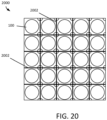
- FIG. 20 illustrates a top view of an example ultrasound transducer device 2000 formed using any of the process flow sequences described herein.
- the transducer device includes an array of individual transducers 100, such as those described above.
- the specific number of transducers 100 shown in FIG. 20 should not be construed in any limiting sense, and may include any number suitable for a desired imaging application, which may be for example on the order of tens, hundreds, thousands, tens of thousands or more. It will be appreciated the above described gettering techniques are particularly beneficial with an increasing larger array, given the ability to provide a uniform cavity pressure across a wafer or die.
- FIG. 20 further illustrates an example location of metal 2002 that may distribute an electrical signal to the membranes (upper electrodes) of the transducers 100.
- the exemplary embodiments illustrate and describe a same bottom electrode metal material used as a getter material during membrane bonding
- other non-metallic or non-metallic alloy getter materials may also be used in a similar manner.
- graphite, phosphorous and/or certain salts may serve as a cavity getter material.
- other locations in addition to a cavity bottom are also contemplated.
- layers may be formed in a manner so as to have getter material disposed on cavity sidewalls and/or the membrane itself (top of sealed cavity) for gettering during membrane bonding. Such additional getter layer(s) may also be formed at a different level than the bottom electrode material.
- the embodiments can be implemented in any of numerous ways.
- the embodiments may be implemented using hardware, software or a combination thereof.
- the software code can be executed on any suitable processor (e.g., a microprocessor) or collection of processors, whether provided in a single computing device or distributed among multiple computing devices.
- any component or collection of components that perform the functions described above can be generically considered as one or more controllers that control the above-discussed functions.
- the one or more controllers can be implemented in numerous ways, such as with dedicated hardware, or with general purpose hardware (e.g., one or more processors) that is programmed using microcode or software to perform the functions recited above.
- certain aspects may be embodied as a method, of which an example has been provided.
- the acts performed as part of the method may be ordered in any suitable way. Accordingly, embodiments may be constructed in which acts are performed in an order different than illustrated, which may include performing some acts simultaneously, even though shown as sequential acts in illustrative embodiments.
- the terms “approximately” and “about” may be used to mean within ⁇ 20% of a target value in some embodiments, within ⁇ 10% of a target value in some embodiments, within ⁇ 5% of a target value in some embodiments, and yet within ⁇ 2% of a target value in some embodiments.
- the terms “approximately” and “about” may include the target value.
Landscapes
- Engineering & Computer Science (AREA)
- Microelectronics & Electronic Packaging (AREA)
- Manufacturing & Machinery (AREA)
- Physics & Mathematics (AREA)
- Health & Medical Sciences (AREA)
- Acoustics & Sound (AREA)
- Life Sciences & Earth Sciences (AREA)
- Signal Processing (AREA)
- Computer Hardware Design (AREA)
- Mechanical Engineering (AREA)
- Biophysics (AREA)
- Veterinary Medicine (AREA)
- Heart & Thoracic Surgery (AREA)
- Medical Informatics (AREA)
- Molecular Biology (AREA)
- Surgery (AREA)
- Animal Behavior & Ethology (AREA)
- General Health & Medical Sciences (AREA)
- Public Health (AREA)
- Biomedical Technology (AREA)
- Radiology & Medical Imaging (AREA)
- Pathology (AREA)
- Nuclear Medicine, Radiotherapy & Molecular Imaging (AREA)
- Gynecology & Obstetrics (AREA)
- Multimedia (AREA)
- Transducers For Ultrasonic Waves (AREA)
- Pressure Sensors (AREA)
- Ultra Sonic Daignosis Equipment (AREA)
Applications Claiming Priority (2)
| Application Number | Priority Date | Filing Date | Title |
|---|---|---|---|
| US201862738502P | 2018-09-28 | 2018-09-28 | |
| PCT/US2019/053352 WO2020069252A1 (en) | 2018-09-28 | 2019-09-27 | Fabrication techniques and structures for gettering materials in ultrasonic transducer cavities |
Publications (4)
| Publication Number | Publication Date |
|---|---|
| EP3856679A1 EP3856679A1 (en) | 2021-08-04 |
| EP3856679A4 EP3856679A4 (en) | 2022-11-02 |
| EP3856679C0 EP3856679C0 (en) | 2024-05-01 |
| EP3856679B1 true EP3856679B1 (en) | 2024-05-01 |
Family
ID=69946946
Family Applications (1)
| Application Number | Title | Priority Date | Filing Date |
|---|---|---|---|
| EP19868109.0A Active EP3856679B1 (en) | 2018-09-28 | 2019-09-27 | Fabrication techniques and structures for gettering materials in ultrasonic transducer cavities |
Country Status (9)
| Country | Link |
|---|---|
| US (1) | US11655141B2 (https=) |
| EP (1) | EP3856679B1 (https=) |
| JP (1) | JP7385652B2 (https=) |
| KR (1) | KR20210070302A (https=) |
| CN (1) | CN112770999A (https=) |
| AU (1) | AU2019350989A1 (https=) |
| CA (1) | CA3111475A1 (https=) |
| TW (1) | TW202042750A (https=) |
| WO (1) | WO2020069252A1 (https=) |
Families Citing this family (16)
| Publication number | Priority date | Publication date | Assignee | Title |
|---|---|---|---|---|
| EP3788798B1 (en) | 2018-05-03 | 2023-07-05 | BFLY Operations, Inc. | Ultrasonic transducers with pressure ports |
| AU2019379545A1 (en) * | 2018-11-13 | 2021-05-27 | Butterfly Network, Inc. | Getter technology for micromachined ultrasonic transducer cavities |
| US11571711B2 (en) | 2018-11-15 | 2023-02-07 | Bfly Operations, Inc. | Anti-stiction bottom cavity surface for micromachined ultrasonic transducer devices |
| WO2020163595A1 (en) | 2019-02-07 | 2020-08-13 | Butterfly Network, Inc | Bi-layer metal electrode for micromachined ultrasonic transducer devices |
| WO2020176149A1 (en) | 2019-02-25 | 2020-09-03 | Butterfly Network, Inc. | Adaptive cavity thickness control for micromachined ultrasonic transducer devices |
| US11484911B2 (en) | 2019-04-12 | 2022-11-01 | Bfly Operations, Inc. | Bottom electrode via structures for micromachined ultrasonic transducer devices |
| US12515240B2 (en) | 2019-04-12 | 2026-01-06 | Bfly Operations, Inc. | Segmented getter openings for micromachined ultrasound transducer devices |
| US11501562B2 (en) | 2019-04-30 | 2022-11-15 | Bfly Operations, Inc. | Ultrasound face scanning and identification apparatuses and methods |
| US11684951B2 (en) | 2019-08-08 | 2023-06-27 | Bfly Operations, Inc. | Micromachined ultrasonic transducer devices having truncated circle shaped cavities |
| US11988640B2 (en) | 2020-03-11 | 2024-05-21 | Bfly Operations, Inc. | Bottom electrode material stack for micromachined ultrasonic transducer devices |
| TW202210830A (zh) | 2020-04-16 | 2022-03-16 | 美商蝴蝶網路公司 | 用於超音波裝置中之電路系統及/或換能器之內建自測試的方法和電路系統 |
| US20210403321A1 (en) * | 2020-06-30 | 2021-12-30 | Butterfly Network, Inc. | Formation of self-assembled monolayer for ultrasonic transducers |
| CN112461438A (zh) * | 2020-12-11 | 2021-03-09 | 中国科学院空天信息创新研究院 | 高灵敏度谐振式差压传感器及其制备方法 |
| TW202240165A (zh) | 2021-03-04 | 2022-10-16 | 美商蝴蝶營運公司 | 具有柱腳的微加工超音波換能器 |
| US12246348B2 (en) | 2021-03-04 | 2025-03-11 | BFLY Operations, Inc | Capacitive Micromachined ultrasonic transducers (CMUTs) having non-uniform pedestals |
| CN113731779B (zh) * | 2021-07-30 | 2022-06-10 | 中北大学 | 基于soi埋氧层牺牲释放技术的电容式微机械超声换能器及其制备方法 |
Family Cites Families (45)
| Publication number | Priority date | Publication date | Assignee | Title |
|---|---|---|---|---|
| JPH08330607A (ja) * | 1995-05-29 | 1996-12-13 | Matsushita Electric Works Ltd | 小型半導体デバイス及び小型赤外線センサ |
| US6430109B1 (en) | 1999-09-30 | 2002-08-06 | The Board Of Trustees Of The Leland Stanford Junior University | Array of capacitive micromachined ultrasonic transducer elements with through wafer via connections |
| US6694817B2 (en) | 2001-08-21 | 2004-02-24 | Georgia Tech Research Corporation | Method and apparatus for the ultrasonic actuation of the cantilever of a probe-based instrument |
| US6779387B2 (en) | 2001-08-21 | 2004-08-24 | Georgia Tech Research Corporation | Method and apparatus for the ultrasonic actuation of the cantilever of a probe-based instrument |
| US6958255B2 (en) | 2002-08-08 | 2005-10-25 | The Board Of Trustees Of The Leland Stanford Junior University | Micromachined ultrasonic transducers and method of fabrication |
| US6836020B2 (en) | 2003-01-22 | 2004-12-28 | The Board Of Trustees Of The Leland Stanford Junior University | Electrical through wafer interconnects |
| JP2005235452A (ja) * | 2004-02-17 | 2005-09-02 | Toshiba Corp | 表示装置 |
| US7615834B2 (en) | 2006-02-28 | 2009-11-10 | The Board Of Trustees Of The Leland Stanford Junior University | Capacitive micromachined ultrasonic transducer(CMUT) with varying thickness membrane |
| JP2009088254A (ja) * | 2007-09-28 | 2009-04-23 | Toshiba Corp | 電子部品パッケージ及び電子部品パッケージの製造方法 |
| US7843022B2 (en) | 2007-10-18 | 2010-11-30 | The Board Of Trustees Of The Leland Stanford Junior University | High-temperature electrostatic transducers and fabrication method |
| US8483014B2 (en) | 2007-12-03 | 2013-07-09 | Kolo Technologies, Inc. | Micromachined ultrasonic transducers |
| AU2009243918A1 (en) | 2008-05-07 | 2009-11-12 | Signostics Limited | Docking system for medical diagnostic scanning using a handheld device |
| US8402831B2 (en) | 2009-03-05 | 2013-03-26 | The Board Of Trustees Of The Leland Standford Junior University | Monolithic integrated CMUTs fabricated by low-temperature wafer bonding |
| JP2011029910A (ja) * | 2009-07-24 | 2011-02-10 | Seiko Instruments Inc | 圧電振動子、圧電振動子の製造方法、発振器、電子機器および電波時計 |
| JP5534398B2 (ja) * | 2009-08-25 | 2014-06-25 | エスアイアイ・クリスタルテクノロジー株式会社 | パッケージ及びパッケージの製造方法、圧電振動子、発振器、電子機器、並びに電波時計 |
| US8241931B1 (en) | 2009-10-19 | 2012-08-14 | Analog Devices, Inc. | Method of forming MEMS device with weakened substrate |
| JP5404335B2 (ja) | 2009-11-17 | 2014-01-29 | キヤノン株式会社 | 電気機械変換装置及びその作製方法 |
| WO2013049794A1 (en) * | 2011-09-30 | 2013-04-04 | Clean Energy Labs, Llc | Electrically conductive membrane transducer and methods to make and use same |
| ITTO20111100A1 (it) * | 2011-11-30 | 2013-05-31 | St Microelectronics Srl | Dispositivo oscillatore e procedimento di fabbricazione dello stesso |
| US9533873B2 (en) | 2013-02-05 | 2017-01-03 | Butterfly Network, Inc. | CMOS ultrasonic transducers and related apparatus and methods |
| WO2014151525A2 (en) | 2013-03-15 | 2014-09-25 | Butterfly Network, Inc. | Complementary metal oxide semiconductor (cmos) ultrasonic transducers and methods for forming the same |
| US9233839B2 (en) * | 2013-08-01 | 2016-01-12 | Taiwan Semiconductor Manufacturing Company Limited | MEMS device and method of forming the same |
| KR102155695B1 (ko) | 2014-02-12 | 2020-09-21 | 삼성전자주식회사 | 전기 음향 변환기 |
| CA2946133A1 (en) | 2014-04-18 | 2015-10-22 | Butterfly Network, Inc. | Ultrasonic transducers in complementary metal oxide semiconductor (cmos) wafers and related apparatus and methods |
| US9067779B1 (en) | 2014-07-14 | 2015-06-30 | Butterfly Network, Inc. | Microfabricated ultrasonic transducers and related apparatus and methods |
| US9422149B2 (en) * | 2014-07-25 | 2016-08-23 | Semiconductor Manufacturing International (Shanghai) Corporation | Trapped sacrificial structures and methods of manufacturing same using thin-film encapsulation |
| JP2016039512A (ja) | 2014-08-08 | 2016-03-22 | キヤノン株式会社 | 電極が貫通配線と繋がったデバイス、及びその製造方法 |
| US20160009544A1 (en) | 2015-03-02 | 2016-01-14 | Butterfly Network, Inc. | Microfabricated ultrasonic transducers and related apparatus and methods |
| US10427188B2 (en) * | 2015-07-30 | 2019-10-01 | North Carolina State University | Anodically bonded vacuum-sealed capacitive micromachined ultrasonic transducer (CMUT) |
| US9630831B1 (en) * | 2015-10-15 | 2017-04-25 | Taiwan Semiconductor Manufacturing Company Ltd. | Semiconductor sensing structure |
| US9938134B2 (en) | 2016-04-14 | 2018-04-10 | Taiwan Semiconductor Manufacturing Co., Ltd. | Getter electrode to improve vacuum level in a microelectromechanical systems (MEMS) device |
| EP3586093A4 (en) | 2017-02-27 | 2021-01-06 | Butterfly Network, Inc. | CAPACITIVE MICRO-MACHINED ULTRASONIC TRANSDUCERS (CMUT), EQUIPMENT AND ASSOCIATED PROCESSES |
| US10196261B2 (en) | 2017-03-08 | 2019-02-05 | Butterfly Network, Inc. | Microfabricated ultrasonic transducers and related apparatus and methods |
| EP3642611B1 (en) | 2017-06-21 | 2024-02-14 | Butterfly Network, Inc. | Microfabricated ultrasonic transducer having individual cells with electrically isolated electrode sections |
| WO2018237267A1 (en) | 2017-06-23 | 2018-12-27 | Butterfly Network, Inc. | Differential ultrasonic transducer element for ultrasound devices |
| JP2021502846A (ja) | 2017-11-15 | 2021-02-04 | バタフライ ネットワーク,インコーポレイテッド | 超音波装置および超音波デバイスを製造するための方法 |
| EP3745961B1 (en) | 2018-01-30 | 2025-10-01 | BFLY Operations, Inc. | Methods and apparatuses for packaging an ultrasound-on-a-chip |
| US11590532B2 (en) | 2018-03-09 | 2023-02-28 | Bfly Operations, Inc. | Ultrasound transducer devices and methods for fabricating ultrasound transducer devices |
| CN108529550B (zh) * | 2018-04-28 | 2019-12-20 | 北京航天控制仪器研究所 | 基于晶圆键合工艺的圆片级封装mems芯片结构及其加工方法 |
| TW201947717A (zh) | 2018-05-03 | 2019-12-16 | 美商蝴蝶網路公司 | 用於超音波晶片的垂直封裝及相關方法 |
| EP3788798B1 (en) | 2018-05-03 | 2023-07-05 | BFLY Operations, Inc. | Ultrasonic transducers with pressure ports |
| US11986349B2 (en) | 2018-05-03 | 2024-05-21 | Bfly Operations, Inc. | Ultrasound devices |
| JP2021529459A (ja) | 2018-07-06 | 2021-10-28 | バタフライ ネットワーク,インコーポレイテッド | 超音波オンチップをパッケージングする方法及び装置 |
| US12515240B2 (en) | 2019-04-12 | 2026-01-06 | Bfly Operations, Inc. | Segmented getter openings for micromachined ultrasound transducer devices |
| US11484911B2 (en) | 2019-04-12 | 2022-11-01 | Bfly Operations, Inc. | Bottom electrode via structures for micromachined ultrasonic transducer devices |
-
2019
- 2019-09-27 WO PCT/US2019/053352 patent/WO2020069252A1/en not_active Ceased
- 2019-09-27 EP EP19868109.0A patent/EP3856679B1/en active Active
- 2019-09-27 CA CA3111475A patent/CA3111475A1/en active Pending
- 2019-09-27 JP JP2021510705A patent/JP7385652B2/ja active Active
- 2019-09-27 KR KR1020217011234A patent/KR20210070302A/ko not_active Ceased
- 2019-09-27 TW TW108135059A patent/TW202042750A/zh unknown
- 2019-09-27 AU AU2019350989A patent/AU2019350989A1/en not_active Abandoned
- 2019-09-27 CN CN201980062783.7A patent/CN112770999A/zh active Pending
- 2019-09-27 US US16/585,283 patent/US11655141B2/en active Active
Also Published As
| Publication number | Publication date |
|---|---|
| AU2019350989A1 (en) | 2021-03-25 |
| CN112770999A (zh) | 2021-05-07 |
| JP7385652B2 (ja) | 2023-11-22 |
| WO2020069252A1 (en) | 2020-04-02 |
| EP3856679A4 (en) | 2022-11-02 |
| EP3856679A1 (en) | 2021-08-04 |
| US11655141B2 (en) | 2023-05-23 |
| TW202042750A (zh) | 2020-12-01 |
| CA3111475A1 (en) | 2020-04-02 |
| JP2022501877A (ja) | 2022-01-06 |
| KR20210070302A (ko) | 2021-06-14 |
| US20200102214A1 (en) | 2020-04-02 |
| EP3856679C0 (en) | 2024-05-01 |
Similar Documents
| Publication | Publication Date | Title |
|---|---|---|
| EP3856679B1 (en) | Fabrication techniques and structures for gettering materials in ultrasonic transducer cavities | |
| US12263506B2 (en) | Anti-stiction bottom cavity surface for micromachined ultrasonic transducer devices | |
| EP3953064B1 (en) | Segmented getter openings for micromachined ultrasound transducer devices | |
| US11684951B2 (en) | Micromachined ultrasonic transducer devices having truncated circle shaped cavities | |
| EP3880373A1 (en) | Getter technology for micromachined ultrasonic transducer cavities | |
| US11766696B2 (en) | Bi-layer metal electrode for micromachined ultrasonic transducer devices | |
| EP3930923A1 (en) | Adaptive cavity thickness control for micromachined ultrasonic transducer devices | |
| US11383269B2 (en) | Curved micromachined ultrasonic transducer membranes | |
| US20210285917A1 (en) | Bottom electrode material stack for micromachined ultrasonic transducer devices | |
| WO2018128072A1 (ja) | 超音波トランスデューサおよび超音波撮像装置 |
Legal Events
| Date | Code | Title | Description |
|---|---|---|---|
| STAA | Information on the status of an ep patent application or granted ep patent |
Free format text: STATUS: THE INTERNATIONAL PUBLICATION HAS BEEN MADE |
|
| PUAI | Public reference made under article 153(3) epc to a published international application that has entered the european phase |
Free format text: ORIGINAL CODE: 0009012 |
|
| STAA | Information on the status of an ep patent application or granted ep patent |
Free format text: STATUS: REQUEST FOR EXAMINATION WAS MADE |
|
| 17P | Request for examination filed |
Effective date: 20210226 |
|
| AK | Designated contracting states |
Kind code of ref document: A1 Designated state(s): AL AT BE BG CH CY CZ DE DK EE ES FI FR GB GR HR HU IE IS IT LI LT LU LV MC MK MT NL NO PL PT RO RS SE SI SK SM TR |
|
| DAV | Request for validation of the european patent (deleted) | ||
| DAX | Request for extension of the european patent (deleted) | ||
| REG | Reference to a national code |
Ref country code: DE Ref legal event code: R079 Free format text: PREVIOUS MAIN CLASS: B81B0003000000 Ipc: B81B0007000000 Ref country code: DE Ref legal event code: R079 Ref document number: 602019051659 Country of ref document: DE Free format text: PREVIOUS MAIN CLASS: B81B0003000000 Ipc: B81B0007000000 |
|
| A4 | Supplementary search report drawn up and despatched |
Effective date: 20220930 |
|
| RIC1 | Information provided on ipc code assigned before grant |
Ipc: H04R 31/00 20060101ALI20220926BHEP Ipc: H04R 19/00 20060101ALI20220926BHEP Ipc: B06B 1/02 20060101ALI20220926BHEP Ipc: B81C 1/00 20060101ALI20220926BHEP Ipc: B81B 7/00 20060101AFI20220926BHEP |
|
| RAP3 | Party data changed (applicant data changed or rights of an application transferred) |
Owner name: BFLY OPERATIONS, INC. |
|
| GRAP | Despatch of communication of intention to grant a patent |
Free format text: ORIGINAL CODE: EPIDOSNIGR1 |
|
| STAA | Information on the status of an ep patent application or granted ep patent |
Free format text: STATUS: GRANT OF PATENT IS INTENDED |
|
| INTG | Intention to grant announced |
Effective date: 20231121 |
|
| GRAS | Grant fee paid |
Free format text: ORIGINAL CODE: EPIDOSNIGR3 |
|
| GRAA | (expected) grant |
Free format text: ORIGINAL CODE: 0009210 |
|
| STAA | Information on the status of an ep patent application or granted ep patent |
Free format text: STATUS: THE PATENT HAS BEEN GRANTED |
|
| AK | Designated contracting states |
Kind code of ref document: B1 Designated state(s): AL AT BE BG CH CY CZ DE DK EE ES FI FR GB GR HR HU IE IS IT LI LT LU LV MC MK MT NL NO PL PT RO RS SE SI SK SM TR |
|
| REG | Reference to a national code |
Ref country code: GB Ref legal event code: FG4D |
|
| REG | Reference to a national code |
Ref country code: CH Ref legal event code: EP |
|
| REG | Reference to a national code |
Ref country code: IE Ref legal event code: FG4D |
|
| REG | Reference to a national code |
Ref country code: DE Ref legal event code: R096 Ref document number: 602019051659 Country of ref document: DE |
|
| U01 | Request for unitary effect filed |
Effective date: 20240513 |
|
| U07 | Unitary effect registered |
Designated state(s): AT BE BG DE DK EE FI FR IT LT LU LV MT NL PT SE SI Effective date: 20240529 |
|
| PG25 | Lapsed in a contracting state [announced via postgrant information from national office to epo] |
Ref country code: IS Free format text: LAPSE BECAUSE OF FAILURE TO SUBMIT A TRANSLATION OF THE DESCRIPTION OR TO PAY THE FEE WITHIN THE PRESCRIBED TIME-LIMIT Effective date: 20240901 |
|
| PG25 | Lapsed in a contracting state [announced via postgrant information from national office to epo] |
Ref country code: HR Free format text: LAPSE BECAUSE OF FAILURE TO SUBMIT A TRANSLATION OF THE DESCRIPTION OR TO PAY THE FEE WITHIN THE PRESCRIBED TIME-LIMIT Effective date: 20240501 |
|
| PG25 | Lapsed in a contracting state [announced via postgrant information from national office to epo] |
Ref country code: GR Free format text: LAPSE BECAUSE OF FAILURE TO SUBMIT A TRANSLATION OF THE DESCRIPTION OR TO PAY THE FEE WITHIN THE PRESCRIBED TIME-LIMIT Effective date: 20240802 |
|
| PG25 | Lapsed in a contracting state [announced via postgrant information from national office to epo] |
Ref country code: ES Free format text: LAPSE BECAUSE OF FAILURE TO SUBMIT A TRANSLATION OF THE DESCRIPTION OR TO PAY THE FEE WITHIN THE PRESCRIBED TIME-LIMIT Effective date: 20240501 |
|
| PG25 | Lapsed in a contracting state [announced via postgrant information from national office to epo] |
Ref country code: PL Free format text: LAPSE BECAUSE OF FAILURE TO SUBMIT A TRANSLATION OF THE DESCRIPTION OR TO PAY THE FEE WITHIN THE PRESCRIBED TIME-LIMIT Effective date: 20240501 |
|
| PG25 | Lapsed in a contracting state [announced via postgrant information from national office to epo] |
Ref country code: PL Free format text: LAPSE BECAUSE OF FAILURE TO SUBMIT A TRANSLATION OF THE DESCRIPTION OR TO PAY THE FEE WITHIN THE PRESCRIBED TIME-LIMIT Effective date: 20240501 Ref country code: NO Free format text: LAPSE BECAUSE OF FAILURE TO SUBMIT A TRANSLATION OF THE DESCRIPTION OR TO PAY THE FEE WITHIN THE PRESCRIBED TIME-LIMIT Effective date: 20240801 Ref country code: IS Free format text: LAPSE BECAUSE OF FAILURE TO SUBMIT A TRANSLATION OF THE DESCRIPTION OR TO PAY THE FEE WITHIN THE PRESCRIBED TIME-LIMIT Effective date: 20240901 Ref country code: HR Free format text: LAPSE BECAUSE OF FAILURE TO SUBMIT A TRANSLATION OF THE DESCRIPTION OR TO PAY THE FEE WITHIN THE PRESCRIBED TIME-LIMIT Effective date: 20240501 Ref country code: GR Free format text: LAPSE BECAUSE OF FAILURE TO SUBMIT A TRANSLATION OF THE DESCRIPTION OR TO PAY THE FEE WITHIN THE PRESCRIBED TIME-LIMIT Effective date: 20240802 Ref country code: ES Free format text: LAPSE BECAUSE OF FAILURE TO SUBMIT A TRANSLATION OF THE DESCRIPTION OR TO PAY THE FEE WITHIN THE PRESCRIBED TIME-LIMIT Effective date: 20240501 Ref country code: RS Free format text: LAPSE BECAUSE OF FAILURE TO SUBMIT A TRANSLATION OF THE DESCRIPTION OR TO PAY THE FEE WITHIN THE PRESCRIBED TIME-LIMIT Effective date: 20240801 |
|
| U20 | Renewal fee for the european patent with unitary effect paid |
Year of fee payment: 6 Effective date: 20240927 |
|
| PG25 | Lapsed in a contracting state [announced via postgrant information from national office to epo] |
Ref country code: CZ Free format text: LAPSE BECAUSE OF FAILURE TO SUBMIT A TRANSLATION OF THE DESCRIPTION OR TO PAY THE FEE WITHIN THE PRESCRIBED TIME-LIMIT Effective date: 20240501 |
|
| PG25 | Lapsed in a contracting state [announced via postgrant information from national office to epo] |
Ref country code: SK Free format text: LAPSE BECAUSE OF FAILURE TO SUBMIT A TRANSLATION OF THE DESCRIPTION OR TO PAY THE FEE WITHIN THE PRESCRIBED TIME-LIMIT Effective date: 20240501 Ref country code: RO Free format text: LAPSE BECAUSE OF FAILURE TO SUBMIT A TRANSLATION OF THE DESCRIPTION OR TO PAY THE FEE WITHIN THE PRESCRIBED TIME-LIMIT Effective date: 20240501 |
|
| PG25 | Lapsed in a contracting state [announced via postgrant information from national office to epo] |
Ref country code: SM Free format text: LAPSE BECAUSE OF FAILURE TO SUBMIT A TRANSLATION OF THE DESCRIPTION OR TO PAY THE FEE WITHIN THE PRESCRIBED TIME-LIMIT Effective date: 20240501 |
|
| PG25 | Lapsed in a contracting state [announced via postgrant information from national office to epo] |
Ref country code: SM Free format text: LAPSE BECAUSE OF FAILURE TO SUBMIT A TRANSLATION OF THE DESCRIPTION OR TO PAY THE FEE WITHIN THE PRESCRIBED TIME-LIMIT Effective date: 20240501 Ref country code: SK Free format text: LAPSE BECAUSE OF FAILURE TO SUBMIT A TRANSLATION OF THE DESCRIPTION OR TO PAY THE FEE WITHIN THE PRESCRIBED TIME-LIMIT Effective date: 20240501 Ref country code: RO Free format text: LAPSE BECAUSE OF FAILURE TO SUBMIT A TRANSLATION OF THE DESCRIPTION OR TO PAY THE FEE WITHIN THE PRESCRIBED TIME-LIMIT Effective date: 20240501 Ref country code: CZ Free format text: LAPSE BECAUSE OF FAILURE TO SUBMIT A TRANSLATION OF THE DESCRIPTION OR TO PAY THE FEE WITHIN THE PRESCRIBED TIME-LIMIT Effective date: 20240501 |
|
| REG | Reference to a national code |
Ref country code: DE Ref legal event code: R097 Ref document number: 602019051659 Country of ref document: DE |
|
| PLBE | No opposition filed within time limit |
Free format text: ORIGINAL CODE: 0009261 |
|
| STAA | Information on the status of an ep patent application or granted ep patent |
Free format text: STATUS: NO OPPOSITION FILED WITHIN TIME LIMIT |
|
| 26N | No opposition filed |
Effective date: 20250204 |
|
| PG25 | Lapsed in a contracting state [announced via postgrant information from national office to epo] |
Ref country code: MC Free format text: LAPSE BECAUSE OF FAILURE TO SUBMIT A TRANSLATION OF THE DESCRIPTION OR TO PAY THE FEE WITHIN THE PRESCRIBED TIME-LIMIT Effective date: 20240501 |
|
| REG | Reference to a national code |
Ref country code: CH Ref legal event code: PL |
|
| GBPC | Gb: european patent ceased through non-payment of renewal fee |
Effective date: 20240927 |
|
| PG25 | Lapsed in a contracting state [announced via postgrant information from national office to epo] |
Ref country code: GB Free format text: LAPSE BECAUSE OF NON-PAYMENT OF DUE FEES Effective date: 20240927 |
|
| PG25 | Lapsed in a contracting state [announced via postgrant information from national office to epo] |
Ref country code: CH Free format text: LAPSE BECAUSE OF NON-PAYMENT OF DUE FEES Effective date: 20240930 |
|
| PG25 | Lapsed in a contracting state [announced via postgrant information from national office to epo] |
Ref country code: IE Free format text: LAPSE BECAUSE OF NON-PAYMENT OF DUE FEES Effective date: 20240927 |
|
| U20 | Renewal fee for the european patent with unitary effect paid |
Year of fee payment: 7 Effective date: 20250929 |
|
| PG25 | Lapsed in a contracting state [announced via postgrant information from national office to epo] |
Ref country code: CY Free format text: LAPSE BECAUSE OF FAILURE TO SUBMIT A TRANSLATION OF THE DESCRIPTION OR TO PAY THE FEE WITHIN THE PRESCRIBED TIME-LIMIT; INVALID AB INITIO Effective date: 20190927 |
|
| U1N | Appointed representative for the unitary patent procedure changed after the registration of the unitary effect |
Representative=s name: CARROLL, CHRISTOPHER P.; GB |
|
| PG25 | Lapsed in a contracting state [announced via postgrant information from national office to epo] |
Ref country code: HU Free format text: LAPSE BECAUSE OF FAILURE TO SUBMIT A TRANSLATION OF THE DESCRIPTION OR TO PAY THE FEE WITHIN THE PRESCRIBED TIME-LIMIT; INVALID AB INITIO Effective date: 20190927 |