EP3845937A1 - Color conversion element - Google Patents
Color conversion element Download PDFInfo
- Publication number
- EP3845937A1 EP3845937A1 EP19853916.5A EP19853916A EP3845937A1 EP 3845937 A1 EP3845937 A1 EP 3845937A1 EP 19853916 A EP19853916 A EP 19853916A EP 3845937 A1 EP3845937 A1 EP 3845937A1
- Authority
- EP
- European Patent Office
- Prior art keywords
- substrate
- phosphor
- conversion element
- color conversion
- reflective layer
- Prior art date
- Legal status (The legal status is an assumption and is not a legal conclusion. Google has not performed a legal analysis and makes no representation as to the accuracy of the status listed.)
- Granted
Links
Images



Classifications
-
- G—PHYSICS
- G02—OPTICS
- G02B—OPTICAL ELEMENTS, SYSTEMS OR APPARATUS
- G02B26/00—Optical devices or arrangements for the control of light using movable or deformable optical elements
- G02B26/007—Optical devices or arrangements for the control of light using movable or deformable optical elements the movable or deformable optical element controlling the colour, i.e. a spectral characteristic, of the light
- G02B26/008—Optical devices or arrangements for the control of light using movable or deformable optical elements the movable or deformable optical element controlling the colour, i.e. a spectral characteristic, of the light in the form of devices for effecting sequential colour changes, e.g. colour wheels
-
- H—ELECTRICITY
- H04—ELECTRIC COMMUNICATION TECHNIQUE
- H04N—PICTORIAL COMMUNICATION, e.g. TELEVISION
- H04N9/00—Details of colour television systems
- H04N9/12—Picture reproducers
- H04N9/31—Projection devices for colour picture display, e.g. using electronic spatial light modulators [ESLM]
- H04N9/3141—Constructional details thereof
- H04N9/315—Modulator illumination systems
- H04N9/3158—Modulator illumination systems for controlling the spectrum
-
- G—PHYSICS
- G02—OPTICS
- G02B—OPTICAL ELEMENTS, SYSTEMS OR APPARATUS
- G02B5/00—Optical elements other than lenses
- G02B5/20—Filters
- G02B5/206—Filters comprising particles embedded in a solid matrix
-
- G—PHYSICS
- G02—OPTICS
- G02B—OPTICAL ELEMENTS, SYSTEMS OR APPARATUS
- G02B5/00—Optical elements other than lenses
- G02B5/20—Filters
- G02B5/28—Interference filters
- G02B5/285—Interference filters comprising deposited thin solid films
-
- G—PHYSICS
- G03—PHOTOGRAPHY; CINEMATOGRAPHY; ANALOGOUS TECHNIQUES USING WAVES OTHER THAN OPTICAL WAVES; ELECTROGRAPHY; HOLOGRAPHY
- G03B—APPARATUS OR ARRANGEMENTS FOR TAKING PHOTOGRAPHS OR FOR PROJECTING OR VIEWING THEM; APPARATUS OR ARRANGEMENTS EMPLOYING ANALOGOUS TECHNIQUES USING WAVES OTHER THAN OPTICAL WAVES; ACCESSORIES THEREFOR
- G03B21/00—Projectors or projection-type viewers; Accessories therefor
- G03B21/14—Details
- G03B21/20—Lamp housings
- G03B21/2006—Lamp housings characterised by the light source
- G03B21/2033—LED or laser light sources
- G03B21/204—LED or laser light sources using secondary light emission, e.g. luminescence or fluorescence
-
- G—PHYSICS
- G03—PHOTOGRAPHY; CINEMATOGRAPHY; ANALOGOUS TECHNIQUES USING WAVES OTHER THAN OPTICAL WAVES; ELECTROGRAPHY; HOLOGRAPHY
- G03B—APPARATUS OR ARRANGEMENTS FOR TAKING PHOTOGRAPHS OR FOR PROJECTING OR VIEWING THEM; APPARATUS OR ARRANGEMENTS EMPLOYING ANALOGOUS TECHNIQUES USING WAVES OTHER THAN OPTICAL WAVES; ACCESSORIES THEREFOR
- G03B21/00—Projectors or projection-type viewers; Accessories therefor
- G03B21/14—Details
- G03B21/20—Lamp housings
- G03B21/2066—Reflectors in illumination beam
-
- H—ELECTRICITY
- H04—ELECTRIC COMMUNICATION TECHNIQUE
- H04N—PICTORIAL COMMUNICATION, e.g. TELEVISION
- H04N9/00—Details of colour television systems
- H04N9/12—Picture reproducers
- H04N9/31—Projection devices for colour picture display, e.g. using electronic spatial light modulators [ESLM]
- H04N9/3141—Constructional details thereof
- H04N9/315—Modulator illumination systems
- H04N9/3152—Modulator illumination systems for shaping the light beam
-
- H—ELECTRICITY
- H04—ELECTRIC COMMUNICATION TECHNIQUE
- H04N—PICTORIAL COMMUNICATION, e.g. TELEVISION
- H04N9/00—Details of colour television systems
- H04N9/12—Picture reproducers
- H04N9/31—Projection devices for colour picture display, e.g. using electronic spatial light modulators [ESLM]
- H04N9/3141—Constructional details thereof
- H04N9/315—Modulator illumination systems
- H04N9/3161—Modulator illumination systems using laser light sources
Definitions
- the present invention aims to provide a color conversion element that is capable of improving the conversion efficiency.
- phosphor portion 3 is formed by planarly arranging a plurality of individual pieces 33, the stress acting upon heating can be dispersed. This suppresses deformation of phosphor portion 3 that occurs when laser light L is received. Therefore, the positional relationship between phosphor portion 3 and air layer 53 can be stabilized, and stable reflectance properties can be maintained.
- recessed portion group 251b is formed in an annular shape about the rotation center of color conversion element 1 in the plan view.
- each of recessed portions 25b included in recessed portion group 251b is formed in a concentric annular shape about the rotation center of color conversion element 1 in the plan view.
- the cross-sectional shape of each recessed portion 25b may be triangular.
- the cross section of each recessed portion 25b may be in any shape.
- the cross-sectional shapes of recessed portions 25b may be different from one another.
- FIG. 8 is a cross-sectional view schematically illustrating the configuration of color conversion element 1E according to Variation 5, more specifically, corresponds to FIG. 2 .
- the structural elements that are substantially the same as the structural elements of color conversion element 1 according to the embodiment share like reference signs. Detailed description of such structural elements will be omitted and only differences are described.
- Variation 5 describes an example in which phosphor portion 3, reflective layer 4, and joining portion 5 are tilted with respect to principal surface 22e of substrate 2e to be oriented outward, they may be tilted to be oriented inward.
- FIG. 9 is a schematic diagram of the configuration of lighting device 100 according to Variation 6. As illustrated in FIG. 9 , lighting device 100 includes light source unit 101, light guide component 102, and color conversion element 1F.
Landscapes
- Physics & Mathematics (AREA)
- Optics & Photonics (AREA)
- General Physics & Mathematics (AREA)
- Engineering & Computer Science (AREA)
- Multimedia (AREA)
- Signal Processing (AREA)
- Astronomy & Astrophysics (AREA)
- Spectroscopy & Molecular Physics (AREA)
- Optical Filters (AREA)
- Projection Apparatus (AREA)
- Non-Portable Lighting Devices Or Systems Thereof (AREA)
Abstract
Description
- The present invention relates to a color conversion element in which a phosphor portion is disposed above a substrate.
- For example, a technique for joining a phosphor portion and a substrate with a heat conductive adhesive to improve heat dissipation of a phosphor wheel (color conversion element) used for a projection device, such as a projector, has been disclosed (for example, see Patent Literature (PTL) 1). In addition, a reflective layer is disposed above the principal surface of the substrate, the principal surface facing the phosphor portion. Therefore, light from the phosphor portion is reflected off the reflective layer and this enhances conversion efficiency.
- PTL 1:
Japanese Unexamined Patent Application Publication No. 2016-99566 - In recent years, further improvement has been desired in the color conversion efficiency of the color conversion element.
- Therefore, the present invention aims to provide a color conversion element that is capable of improving the conversion efficiency.
- A color conversion element according to one aspect of the present invention includes: a substrate; a phosphor portion that is disposed above the substrate, receives laser light transmitted from an outside, and emits light in a color different from a color of the laser light; a reflective layer that includes a dielectric multilayer film and is disposed on a principal surface of the phosphor portion, the principal surface of the phosphor portion being a surface facing the substrate; and a joining portion that is interposed between the reflective layer and the substrate to join the reflective layer and the substrate. The joining portion includes an air layer that exposes the reflective layer in a position where the air layer at least partially overlaps an irradiation region in a plan view, the irradiation region being a region irradiated with the laser light on the phosphor portion.
- The color conversion element according to the present invention improves the conversion efficiency.
-
-
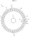
FIG. 1 is a schematic diagram of the configuration of a color conversion element according to an embodiment. -
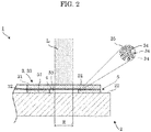
FIG. 2 is a cross-sectional view taken along the line II-II inFIG. 1 . -
FIG. 3 is a cross-sectional view schematically illustrating the configuration of a color conversion element according toVariation 1. -
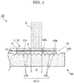
FIG. 4 is a cross-sectional view schematically illustrating the configuration of a color conversion element according toVariation 2. -
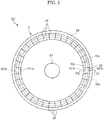
FIG. 5 is a plan view schematically illustrating the configuration of a color conversion element according toVariation 3. -
FIG. 6 is a cross-sectional view schematically illustrating the configuration of the color conversion element according toVariation 3. -
FIG. 7 is a cross-sectional view schematically illustrating the configuration of a color conversion element according toVariation 4. -
FIG. 8 is a cross-sectional view schematically illustrating the configuration of a color conversion element according toVariation 5. -
FIG. 9 is a schematic diagram of the configuration of a lighting device according to Variation 6. - The following describes a color conversion element according to an embodiment of the present invention with reference to the accompanying drawings. Note that the embodiment described below shows specific preferable examples according to the present invention. Therefore, the numerical values, shapes, materials, structural elements, the arrangement and connection of the structural elements, etc. shown in the following embodiment are mere examples, and do not limit the scope of the present invention. Of the structural elements in the following embodiment, structural elements not recited in any one of the independent claims representing broadest concepts of the present invention are described as optional structural elements.
- In addition, each diagram is a schematic diagram and is not necessarily a precise illustration. In each figure, structural elements that are essentially the same share like reference signs.
- Hereinafter, an embodiment will be described.
-
FIG. 1 is a schematic diagram of the configuration of a color conversion element according to the embodiment.FIG. 2 is a cross-sectional view taken along the line II-II inFIG. 1 . -
Color conversion element 1 is a phosphor wheel to be used in a projection device, such as a projector. The projection device includes a semiconductor laser element as a light source unit. The semiconductor laser element emits laser light L having a wavelength in a range of from violet to blue (430 nm to 490 nm) tocolor conversion element 1.Color conversion element 1 uses, as excitation light, laser light L emitted from the light source unit to emit white light. Hereinafter,color conversion element 1 will be described in detail. - As illustrated in
FIGs. 1 and2 ,color conversion element 1 includessubstrate 2,phosphor portion 3,reflective layer 4, and joiningportion 5. Note that inFIGs. 1 and2 , laser light L is illustrated by dot hatching. The region irradiated with laser light L incolor conversion element 1 is called irradiation region R. Irradiation region R is fixed, but seems as if irradiation region R moves circumferentially with respect tocolor conversion element 1 becausecolor conversion element 1 rotates. -
Substrate 2 has, for example, a circular shape in a plan view, and throughhole 21 is formed in a center portion ofsubstrate 2. A rotation shaft in the projection device which is inserted into throughhole 21 allowssubstrate 2 to rotate. -
Substrate 2 has a thermal conductivity higher than the thermal conductivity ofphosphor portion 3. This allows the heat transferred fromphosphor portion 3 to be dissipated efficiently fromsubstrate 2. More specifically,substrate 2 is formed using a metallic material, such as Al, Al2O3, AlN, Fe and Ti. Note thatsubstrate 2 may be formed using a material other than the metallic materials as long as the material has a thermal conductivity higher than the thermal conductivity ofphosphor portion 3. Examples of materials other than the metallic materials include Si, ceramic, sapphire, and graphite. -
Principal surface 22, which is one of the principal surfaces ofsubstrate 2 is flat, andphosphor portion 3 is disposed aboveprincipal surface 22. -
Phosphor portion 3 has a uniform thickness as a whole.Phosphor portion 3, for example, contains, in a dispersed state, phosphor particles (phosphor particles 34) that emit fluorescence when excited by laser lightL. Phosphor particles 34 emit fluorescence when irradiated with laser light L. Therefore, firstprincipal surface 31 ofphosphor portion 3 on the side opposite tosubstrate 2 is the surface through which the fluorescence is emitted. In the present embodiment, the normal direction of secondprincipal surface 32 ofphosphor portion 3 is substantially the same as the direction of laser light L (incident direction) incident onphosphor portion 3. Secondprincipal surface 32 is thesurface facing substrate 2. The term "substantially the same" is not only means exactly the same, but also allows an acceptable error of several percent. In addition, firstprincipal surface 31 ofphosphor portion 3 may have minute projections and recesses throughoutphosphor portion 3. More specifically, the surface roughness of firstprincipal surface 31 may be greater than a predetermined value. As a result, firstprincipal surface 31 ofphosphor portion 3 has a low reflectance, which can improve efficiencies of extraction and reception of light. -
Phosphor portion 3 has an annular shape in the plan view as a whole.Phosphor portion 3 is formed by annularly arrangingindividual pieces 33 having a sheet shape.Individual pieces 33 have a uniform thickness.Individual pieces 33 are identical in shape and of the same type. More specifically, each ofindividual pieces 33 has a trapezoidal shape in the plan view. Note thatindividual pieces 33 may be in any shape as long as individual pieces are sheet-shaped. Examples of other shapes in the plan view ofindividual pieces 33 include a quadrilateral shape, a triangular shape, and other polygonal shapes, for instance. - The adjacent sides of
individual pieces 33 adjacent to each other are substantially coincide with each other.Individual pieces 33 include at least one type ofphosphor particles 34. In the present embodiment,individual pieces 33 emit white light and includes three types ofphosphor particles 34 in a proper ratio: a red phosphor, a yellow phosphor, and a green phosphor. When irradiated with laser light L, the red phosphor emits red light, the yellow phosphor emits yellow light, and the green phosphor emits green light. - While the types and characteristics of
phosphor particles 34 are not particularly limited, phosphor particles having a high thermal resistance is desirable because laser light L used as the excitation light has relatively high output. In addition, while the types ofbase material 35 that holdsphosphor particles 34 in a dispersed state are not particularly limited,base material 35 is desirable to have a high light transmittance for the wavelength of the excitation light and the wavelength of the light emitted fromphosphor particles 34. More specifically, for example, the material ofbase material 35 may be glass or ceramic. Note thatphosphor portion 3 may be a polycrystalline or monocrystalline substance including one type of phosphor. - In addition,
reflective layer 4 that reflects laser light L and light emitted fromphosphor particles 34 is disposed on the entire back surface (the principal surface facing joining portion 5) of eachindividual piece 33.Reflective layer 4 has a uniform thickness. -
Reflective layer 4 is disposed on the back surface of eachindividual piece 33, as previously described. In other words,reflective layer 4 is disposed on the principal surface ofphosphor portion 3 that faces substrate 2 (second principal surface 32).Reflective layer 4 has entirely a uniform thickness.Reflective layer 4 is a dielectric multilayer layer film. The dielectric multilayer film is a multilayer stack including alternating layers of a transparent dielectric material having a high refractive index (n = 2.0 to 3.0) and layers of a transparent dielectric material having a low refractive index (n = 1.0 to 1.9). The dielectric multilayer film can achieve desired reflectance properties by adjusting the refractive index of the materials and the thickness of the dielectric multilayer film. More specifically, the refractive index of the materials and the thickness of the dielectric multilayer layer film are adjusted so that the dielectric multilayer layer film, which formsreflective layer 4, has a high reflectance for laser light L and light emitted fromphosphor particles 34.Reflective layer 4 is disposed on the back surface of eachindividual piece 33, for example, by sputtering or deposition. - Joining
portion 5 is interposed betweenreflective layer 4 andsubstrate 2 to joinreflective layer 4 andsubstrate 2. More specifically, joiningportion 5 is formed using a resin-based adhesive such as a silicon resin, for example. Joiningportion 5 is applied toprincipal surface 22 ofsubstrate 2, and thenreflective layer 4 on eachindividual piece 33 is attached to joiningportion 5. In this manner,individual pieces 33 constitutephosphor portion 3 having an annular shape in the plan view abovesubstrate 2. In this state,reflective layer 4 onindividual pieces 33 is also formed into an annular shape in the plan view in accordance with the shape ofphosphor portion 3. - Joining
portion 5 includes first joiningportion 51 and second joiningportion 52. First joiningportion 51 and second joiningportion 52 have a uniform thickness. First joiningportion 51 and second joiningportion 52 each have a concentric annular shape and are spaced apart by a predetermined distance in the radial direction. First joiningportion 51 has a smaller diameter than second joiningportion 52. First joiningportion 51 is located in a more inward position than second joiningportion 52. First joiningportion 51 joinssubstrate 2 and an inner peripheral portion ofreflective layer 4. The inner peripheral portion ofreflective layer 4 is located in a more inward position than irradiation region R. - On the other hand, second joining
portion 52 has a larger diameter than first joiningportion 51 and is located in a more outward position than first joiningportion 51. Second joiningportion 52 joinssecond substrate 2 and an outer peripheral portion ofreflective layer 4. The outer peripheral portion ofreflective layer 4 is located in a more outward position than irradiation region R. -
Air layer 53 is formed between first joiningportion 51 and second joiningportion 52.Air layer 53 has an annular shape concentric with first joiningportion 51 and second joiningportion 52. The centers of first joiningportion 51, second joiningportion 52, andair layer 53 are the rotation center ofcolor conversion element 1.Air layer 53 is sealed by first joiningportion 51 and second joiningportion 52, because first joiningportion 51 and second joiningportion 52 are each a continuous, integrated component along the peripheral direction. -
Air layer 53 exposesreflective layer 4 andsubstrate 2. In other words,reflective layer 4 andsubstrate 2 are in contact with air byair layer 53. -
Air layer 53 is located in a position whereair layer 53 at least partially overlaps irradiation region R in the plan view. In the present embodiment,air layer 53 is formed in a position and in a size that includes irradiation region R entirely in the plan view. As described above,air layer 53 has an annular shape about the rotation center ofcolor conversion element 1. Therefore, whencolor conversion element 1 rotates,air layer 53 always overlaps irradiation region R in the plan view. - The following describes the operations of the projection device.
- When laser light L is emitted from the light source of the projection device,
color conversion element 1 receives laser light L atphosphor portion 3 whilecolor conversion element 1 is rotating. A portion of laser light L directly incidents onphosphor particles 34 inphosphor portion 3. In addition, another portion of laser light L that does not directly incident onphosphor particles 34 is reflected offreflective layer 4 and incidents onphosphor particles 34.Phosphor particles 34 convert laser light L that has reachedphosphor particles 34 into white light and emit the white light. A portion of the white light emitted fromphosphor particles 34 is directly emitted fromphosphor portion 3 to the outside. Another portion of the light emitted fromphosphor particles 34 is also emitted fromphosphor portion 3 to the outside by being reflected offreflective layer 4. - Here, there is a small amount of light that passes through
reflective layer 4, which includes a dielectric multilayer film. To prevent this,air layer 53 is provided in joiningportion 5. In detail, in irradiation region R, as described above,air layer 53 is located directly belowreflective layer 4. In this case, critical angle θc is expressed by Snell's law by the following expression (1):

phosphor portion 3 from which light enters is 1.8, and refractive index n2 ofair layer 53 to which the light transmits is 1.0, critical angle θc is 33.8 degrees. Note that the thicknesses of the adhesive layer andreflective layer 4 are very thin compared with the thickness ofphosphor portion 3 or the thickness ofair layer 53, and has an insignificant effect on critical angle θc. Therefore, such thickness is ignored in the calculation of critical angle θc. - On the other hand, when there is no
air layer 53 in joiningportion 5 is assumed. In other words, in irradiation region R, joiningportion 5 is located directly belowreflective layer 4 andreflective layer 4 is not exposed. In this case, if refractive index n1 ofphosphor portion 3 from which light enters is 1.8, and refractive index n2 of joiningportion 5 to which the light transmits is 1.4 (the refractive index when joiningportion 5 is a silicon resin), critical angle θc is 51.1 degrees. - Thus, critical angle θc can be reduced in the present embodiment compared with when
air layer 53 is not provided in joiningportion 5. In other words, it is possible to increase the range (90 degrees - θc) of the incident angle of the total internal reflection. As described above, not only laser light L directly entersreflective layer 4, but also white light emitted by eachphosphor particle 34 entersreflective layer 4. Although the incident angle of the white light with respect toreflective layer 4 is varied, more white light can be totally, internally reflected if the range of the incident angle of total internal reflection is increased. Therefore, the reflectance ofreflective layer 4, which is a dielectric multilayer film, can be increased. - As described above,
color conversion element 1 according to the present embodiment includes:substrate 2;phosphor portion 3 that is disposed abovesubstrate 2, receives laser light L transmitted from an outside, and emits light in a color different from a color of laser light L;reflective layer 4 that includes a dielectric multilayer film and is disposed on a principal surface ofphosphor portion 3, the principal surface ofphosphor portion 3 being asurface facing substrate 2; and joiningportion 5 that is interposed betweenreflective layer 4 andsubstrate 2 to joinreflective layer 4 andsubstrate 2. Joiningportion 5 includesair layer 53 that exposesreflective layer 4 in a position whereair layer 4 at least partially overlaps irradiation region R in a plan view, irradiation region R being a region irradiated with laser light L onphosphor portion 3. - With this, since
air layer 53 at least partially overlaps irradiation region R in the plan view, it is possible to increase the range (90 degrees - θc) of the incident angle of total internal reflection compared with whenair layer 53 is not provided. Therefore, the reflectance ofreflective layer 4, which is a dielectric multilayer layer film, can be increased, and conversion efficiency can also be increased. - In particular, in the present embodiment,
air layer 53 is formed in a position and a size that includes irradiation region R entirely in the plan view. Therefore, the reflectance can be increased for the entire irradiation region R. In other words, conversion efficiency can be further increased. - Furthermore,
phosphor portion 3 includes a plurality ofindividual pieces 33 having a sheet shape and being planarly arranged, the plurality of individual pieces including at least one type of phosphor (phosphor particles 34). - With this, since
phosphor portion 3 is formed by planarly arranging a plurality ofindividual pieces 33, the stress acting upon heating can be dispersed. This suppresses deformation ofphosphor portion 3 that occurs when laser light L is received. Therefore, the positional relationship betweenphosphor portion 3 andair layer 53 can be stabilized, and stable reflectance properties can be maintained. - Here, when a phosphor portion that is entirely integrally formed is used and its shape is annular in the plan view, such an integrated phosphor portion is easily affected by the stress concentration and the above problem is likely to occur. However, as in the present embodiment,
phosphor portion 3 formed by arrangingindividual pieces 33 in an annular shape can disperse stress, thus achieving a high stress relief effect. - Note that in the above embodiment, an example in which
phosphor portion 3 includesindividual pieces 33 is described. However, the phosphor portion may be integrally molded as a whole. - Next,
Variation 1 will be described.FIG. 3 is a cross-sectional view schematically illustrating the configuration ofcolor conversion element 1A according toVariation 1, and more specifically, corresponds toFIG. 2 . In the following description, the structural elements that are substantially the same as the structural elements ofcolor conversion element 1 according to the embodiment share like reference signs. Detailed description of such structural elements will be omitted and only differences are described. - In the above embodiment, an example in which
principal surface 22 ofsubstrate 2 is flat has been described.Variation 1 describes an example in which recessedportion 25a is formed inprincipal surface 22a ofsubstrate 2a. - More specifically, recessed
portion 25a is provided inprincipal surface 22a ofsubstrate 2a and located in a position where recessedportion 25a at least partially overlap irradiation region R in the plan view. In the present embodiment, recessedportion 25a is formed in a position and a size that include the entire irradiation region R in the plan view. Recessedportion 25a is formed in an annular shape about the rotation center ofcolor conversion element 1 in the plan view. In other words, recessedportion 25a is an annular continuous groove in the plan view. Recessedportion 25a has a quadrilateral shape in a cross-sectional view.Air layer 53a is provided above recessedportion 25a. The cross section of recessedportion 25a may be in any shape. - Joining
portion 5a partially flows into recessedportion 25a during manufacture. Such partial flow of joiningportion 5a into recessedportion 25a ensures thatair layer 53a is formed in a position where recessedportion 25a overlaps irradiation region R in the plan view. Note that whileFIG. 3 illustrates a state where part of joiningportion 5a is filled into the entire recessedportion 25a, joiningportion 5a may be divided in recessedportion 25a. In any case, the presence of recessedportion 25a ensures the formation ofair layer 53a, which exposesreflective layer 4. - Next,
Variation 2 will be described.FIG. 4 is a cross-sectional view schematically illustrating the configuration ofcolor conversion element 1B according toVariation 2, and more specifically, corresponds toFIG. 2 . In the following description, the structural elements that are substantially the same as the structural elements ofcolor conversion element 1 according to the embodiment share like reference signs. Detailed description of such structural elements will be omitted and only differences are described. - In the embodiment, an example in which
principal surface 22 ofsubstrate 2 is flat has been described.Variation 1 describes an example in which recessedportion group 251b including a plurality of recessedportions 25b is provided inprincipal surface 22b ofsubstrate 2b. - More specifically, recessed
portion group 251b is provided inprincipal surface 22b ofsubstrate 2a and located in a position where recessedportion group 251b at least partially overlaps irradiation region R in a plan view. In the present embodiment, recessedportion group 251b is formed in a position and in a size that include theentire phosphor portion 3 in the plan view. Therefore, the entire irradiation region R overlaps recessedportion group 251b in the plan view. Air layer 53b is provided above recessedportion group 251b. - In addition, recessed
portion group 251b is formed in an annular shape about the rotation center ofcolor conversion element 1 in the plan view. Here, each of recessedportions 25b included in recessedportion group 251b is formed in a concentric annular shape about the rotation center ofcolor conversion element 1 in the plan view. The cross-sectional shape of each recessedportion 25b may be triangular. The cross section of each recessedportion 25b may be in any shape. Furthermore, the cross-sectional shapes of recessedportions 25b may be different from one another. - First joining
portion 51b and second joiningportion 52b of joiningportion 5b are applied to recessedportion group 251b during manufacture. Here, at the boundary of air layer 53b, the peak portions ofadjacent recesses 25b serve as walls, preventing first joiningportion 51b and second joiningportion 52b from entering more inward thanrecesses 25b. Therefore, air layer 53b can be reliably secured. Furthermore, each of first joiningportion 51b and second joiningportion 52b is continuously formed on recessedportions 25b. This means that the contact area between first joiningportion 51b andsubstrate 2b and the contact area between second joiningportion 52b andsubstrate 2b can be increased. This improves heat dissipation and adhesion, and improves the reliability ofcolor conversion element 1B. - Next,
Variation 3 will be described.FIG. 5 is a plan view schematically illustrating the configuration ofcolor conversion element 1C according toVariation 3, more specifically, corresponds toFIG. 1 .FIG. 6 is a cross-sectional view schematically illustrating the configuration ofcolor conversion element 1C according toVariation 3, more specifically, corresponds toFIG. 2 . In the following description, the structural elements that are substantially the same as the structural elements ofcolor conversion element 1 according to the embodiment share like reference signs. Detailed description of such structural elements will be omitted and only differences are described. - In the embodiment, an example in which
air layer 53 is sealed by first joiningportion 51 and second joiningportion 52 of joiningportion 5 has been described.Variation 3 describes an unsealedair layer 53c. - More specifically, in joining
portion 5c according toVariation 3, a pair ofcommunication holes 511c at opposite positions across the center are formed in first joiningportion 51c. The pair ofcommunication holes 511c extend along the diameter and pass through first joiningportion 51c. On the other hand, in second joiningportion 52c, a pair ofcommunication holes 521c are formed at opposite positions across the center. The pair ofcommunication holes 521c extend along the diameter and pass through second joiningportion 52c. The pair ofcommunication holes 511c in first joiningportion 51c and the pair ofcommunication holes 521c in second joiningportion 52c are collinear.Air layer 53c is in commutation with the outside bycommunication holes - Accordingly, joining
portion 5c includes communication holes 511c and 521c that communicateair layer 53c with the outside. Therefore, communication holes 511c and 521c can be used as air paths. For example, if air inair layer 53c is heated and expanded during irradiation of laser light L or during manufacture, the air is released fromcommunication holes air layer 53c can be kept constant. Therefore, it is possible to suppress the delamination of joiningportion 5c due to the shape change ofair layer 53c, thereby increasing the reliability ofcolor conversion element 1C. Note that any number of through holds may be provided at any locations. - Next,
Variation 4 will be described.FIG. 7 is a cross-sectional view schematically illustrating the configuration ofcolor conversion element 1D according toVariation 4, more specifically, corresponds toFIG. 2 . In the following description, the structural elements that are substantially the same as the structural elements ofcolor conversion element 1 according to the embodiment share like reference signs. Detailed description of such structural elements will be omitted and only differences are described. - In the embodiment, an example in which joining
portion 5 joinssubstrate 2 and the outer peripheral portion ofreflective layer 4, which is located in a more outward position than irradiation region R, and also joinssubstrate 2 and the inner peripheral portion ofreflective layer 4, which is located in a more inward position than irradiation region R, has been described.Variation 4 describes when joiningportion 5d joins onlysubstrate 2 and the outer peripheral portion ofreflective layer 4 located outward from irradiation region R. - More specifically, joining
portion 5d is formed in an annular shape in a plan view so that the outer peripheral portion ofreflective layer 4, which is located in a more outward position than irradiation region R, joins withsubstrate 2. Therefore, the portion that is more inward than joiningportion 5d becomesair layer 53d as a whole. In this case, betweensubstrate 2 and the inner peripheral portion ofreflective layer 4, which is located in a more inward position than irradiation region R, can be considered as communication hole. In other words, an effect can be obtained that is similar to the effect obtained by providingcommunication holes - Moreover, when
color conversion element 1D is a phosphor wheel,color conversion element 1D rotates. In this case, since only the outer peripheral portion ofcolor conversion element 1D has joiningportion 5d, joiningportion 5d can remain stable even if the centrifugal force caused by rotation is applied. This means that the amount of adhesive to be used can be reduced. - Next,
Variation 5 will be described.FIG. 8 is a cross-sectional view schematically illustrating the configuration ofcolor conversion element 1E according toVariation 5, more specifically, corresponds toFIG. 2 . In the following description, the structural elements that are substantially the same as the structural elements ofcolor conversion element 1 according to the embodiment share like reference signs. Detailed description of such structural elements will be omitted and only differences are described. - In the embodiment, the example in which first
principal surface 31 and secondprincipal surface 32 ofphosphor portion 3 are not tilted with respect toprincipal surface 22 ofsubstrate 2 has been described.Variation 5 describes when firstprincipal surface 31 and secondprincipal surface 32 ofphosphor portion 3 are tilted with respect toprincipal surface 22e ofsubstrate 2e.Phosphor portion 3,reflective layer 4, and joiningportion 5 inVariation 5 are the same as those in the embodiment, except for their orientations with respect tosubstrate 2e. Therefore,phosphor portion 3,reflective layer 4, and joiningportion 5 are described using like reference signs. - More specifically, in
principal surface 22e ofsubstrate 2e according toVariation 5, recessedportion 29e is formed to accommodatephosphor portion 3,reflective layer 4, and joiningportion 5. Recessedportion 29e is formed in an annular shape about the rotation center in the plan view. Recessedportion 29e is recessed such that its bottom surface faces outward with respect toprincipal surface 22e ofsubstrate 2e, and its inner peripheral surface and outer peripheral surface are perpendicular to its bottom surface in a cross-sectional view. Accommodatingphosphor portion 3,reflective layer 4, and joiningportion 5 in recessedportion 29e makesphosphor portion 3,reflective layer 4, and joiningportion 5 tilt with respect toprincipal surface 22e ofsubstrate 2e. More specifically, first joiningportion 51 of joiningportion 5 is disposed on an inner peripheral portion of the bottom surface of recessedportion 29e, and second joiningportion 52 is disposed on an outer peripheral portion of the bottom surface of recessedportion 29e. Between first joiningportion 51 and second joiningportion 52 isair layer 53.Reflective layer 4 and joiningportion 5 are disposed on first joiningportion 51 and second joiningportion 52. In this manner, firstprincipal surface 31 and secondprincipal surface 32 ofphosphor portion 3 are parallel to the bottom surface of recessedportion 29e. In other words,phosphor portion 3 is embedded in recessedportion 29e to be oriented outward with respect toprincipal surface 22e ofsubstrate 2e.Phosphor portion 3 partially protrudes from recessedportion 29e, while the rest is embedded in recessedportion 29e. The inner and outer sides ofphosphor portion 3 are in contact withsubstrate 2e in recessedportion 29e. This allows heat to be transferred from the inner and outer sides ofphosphor portion 3 tosubstrate 2e. -
Phosphor portion 3 is disposed abovesubstrate 2e and oriented such that normal direction N of secondprincipal surface 32 ofphosphor portion 3, which is asurface facing substrate 2e, is tilted with respect to incident direction I of laser light L onphosphor portion 3. Here, angle α between normal direction N and incident direction I is greater than or equal to critical angle θc between air andphosphor portion 3. As a result, laser light L entersphosphor portion 3 with an incident angle that causes total internal reflection of laser light L, thus increasing the reflectance atreflective layer 4. - As described above,
phosphor portion 3 is disposed abovesubstrate 2e and oriented such that normal direction N of the principal surface (second principal surface 32) ofphosphor portion 3, which is asurface facing substrate 2e, is tilted with respect to incident direction I of laser light L onphosphor portion 3. - With this, normal direction N of second
principal surface 32 ofphosphor portion 3 is tilted with respect to incident direction I of laser light L, making it easier to reflect all laser light L offreflective layer 4. This improves the reflectance atreflective layer 4, thereby increasing the conversion efficiency. - Moreover, angle α between normal direction N and incident direction I is greater than or equal to critical angle θc between air and
phosphor portion 3. - With this, laser light L enters
phosphor portion 3 at the incident angle that causes total internal reflection. This reliably increases the reflectance atreflective layer 4. Therefore, conversion efficiency can be further increased. - Moreover,
phosphor portion 3 is embedded insubstrate 2e with a side being at least partially in contact withsubstrate 2e. - This allows heat to be transferred from the inner and outer sides of
phosphor portion 3 tosubstrate 2e, thereby further increasing heat dissipation. - Note that while
Variation 5 describes an example in whichphosphor portion 3,reflective layer 4, and joiningportion 5 are tilted with respect toprincipal surface 22e ofsubstrate 2e to be oriented outward, they may be tilted to be oriented inward. - In
Variation 5, an example has been described in whichphosphor portion 3 is tilted with respect toprincipal surface 22e ofsubstrate 2e to tilt normal direction N of secondprincipal surface 32 ofphosphor portion 3, which is asurface facing substrate 2e, with respect to incident direction I of laser light L onphosphor portion 3. However, the incident direction of laser light L may be tilted with respect to secondprincipal surface 32 ofphosphor portion 3 to tilt normal direction N with respect to incident direction I. - Note that also in
Variation 5, the phosphor portion may be an integrally molded element as a whole. - In the embodiment, while the example in which
color conversion element 1 is applied to a projection device has been described, the color conversion element may be used in a lighting device as well. In this case, the color conversion element need not be in a wheel shape, because the color conversion element does not rotate. The following is an example of a color conversion element used in a lighting device. -
FIG. 9 is a schematic diagram of the configuration oflighting device 100 according to Variation 6. As illustrated inFIG. 9 ,lighting device 100 includeslight source unit 101,light guide component 102, and color conversion element 1F. -
Light source unit 101 generates laser light L1 and supplies laser light L1 to color conversion element 1F vialight guide component 102. For example,light source unit 101 is a semiconductor laser element that emits laser light L1 having a wavelength in a range of from violet to blue (430 nm to 490 nm).Light guide component 102 is a light guide component that guides laser light L1 emitted bylight source unit 101 to color conversion element 1F.Light guide component 102 is, for example, an optical fiber. -
Substrate 2f of color conversion element 1F is quadrilateral in a plan view. Onprincipal surface 22f, which is one of the principal surfaces ofsubstrate 2f,reflective layer 4f andphosphor portion 3f are stacked via joiningportion 5f.Phosphor portion 3f is formed in a quadrilateral shape in the plan view, andreflective layer 4f that includes a dielectric multilayer film is disposed on the entire principal surface ofphosphor portion 3. The principal surface is asurface facing substrate 2f. Joiningportion 5f is formed in a frame shape that is continuous along the outer peripheral portion ofphosphor portion 3f. This createsair layer 53f, which exposesreflective layer 4f, in the inward portion of joiningportion 5f.Air layer 53f is located in a position whereair layer 53f overlaps irradiation region R1 of laser light L1 in the plan view. - Accordingly, in
lighting device 100 according to Variation 6,reflective layer 4f is exposed in a position whereair layer 53f at least partially overlaps irradiation region R1 onphosphor portion 3f in the plan view. Therefore, it is possible to increase the range (90 degrees - θc) of the incident angle that causes total internal reflection, compared with whenair layer 53f is not provided. Therefore, the reflectance ofreflective layer 4f, which is a dielectric multilayer film, can be increased, and conversion efficiency can also be improved. - Note that the phosphor portion in the color conversion element used in the lighting device may also include a plurality of individual pieces.
- The lighting device according to one or more aspects of the present invention has been described above on the basis of the embodiment and the variations, but the present invention is not limited to the embodiment and the variations.
- For example, a reflection suppression layer such as an anti-reflection (AR) coating layer may be disposed on first
principal surface 31 ofphosphor portion 3. Firstprincipal surface 31 is a surface from which light is emitted. This improves light extraction efficiency. - In the embodiment, an example in which
phosphor portion 3 includingindividual pieces 33 that emit white light as a whole has been described. However, when the phosphor portion emits a plurality of colors, an area that emits the same color inphosphor portion 3 may include individual pieces of the same type. For example, a phosphor portion including three layers of red, green, and blue phosphor portions that are planarly arranged. The red phosphor portion includes a plurality of individual pieces of the same type, i.e., individual pieces including a red phosphor. The blue phosphor portion includes a plurality of individual pieces of the same type, i.e., individual pieces including a blue phosphor. The green phosphor portion includes a plurality of individual pieces of the same type, i.e., individual pieces including a green phosphor. - The scope of the present invention may also include other embodiments implemented through various changes and modifications conceived by a person of ordinary skill in the art based on the aforementioned embodiment, and embodiments obtained by combining the structural elements and functions in the aforementioned embodiment and
Variations 1 to 3 in any manner within a scope not departing from the scope of the present invention. -
- 1, 1A, 1B, 1C, 1D, 1E, 1F
- color conversion element
- 2, 2a, 2b, 2e, 2f
- substrate
- 3, 3f
- phosphor portion
- 4,4f
- reflective layer
- 5, 5a, 5b, 5c, 5d, 5f
- joining portion
- 21
- through hole
- 22, 22a, 22b, 22e, 22f
- principal surface
- 25A, 25b, 29e
- recessed portion
- 32
- second principal surface (principal surface)
- 53, 53a, 53b, 53c, 53d, 53f
- air layer
- 251b
- recessed portion group
- 511c, 521c
- communication hole
- I
- incident direction
- L, L1
- laser light
- N
- normal direction
- R, R1
- irradiation region
Claims (9)
- A color conversion element, comprising:a substrate;a phosphor portion that is disposed above the substrate, receives laser light transmitted from an outside, and emits light in a color different from a color of the laser light;a reflective layer that includes a dielectric multilayer film and is disposed on a principal surface of the phosphor portion, the principal surface of the phosphor portion being a surface facing the substrate; anda joining portion that is interposed between the reflective layer and the substrate to join the reflective layer and the substrate, whereinthe joining portion includes an air layer that exposes the reflective layer in a position where the air layer at least partially overlaps an irradiation region in a plan view, the irradiation region being a region irradiated with the laser light on the phosphor portion.
- The color conversion element according to claim 1, wherein
a recessed portion is provided in a principal surface of the substrate in a position where the recessed portion at least partially overlaps the irradiation region in the plan view, and the air layer is provided above the recessed portion, the principal surface of the substrate being a surface facing the phosphor portion. - The color conversion element according to claim 1, wherein
a recessed portion group including a plurality of recessed portions is provided on the principal surface of the substrate in a position where the recessed portion group at least partially overlaps the irradiation region in the plan view, and the air layer is provided above the recessed portion group. - The color conversion element according to any one of claims 1 to 3, wherein
the joining portion includes a communication hole that communicates the air layer with the outside. - The color conversion element according to any one of claims 1 to 4, wherein
the phosphor portion and the reflective layer each have an annular shape in the plan view, and
the joining portion only joins the substrate and an outer peripheral portion of the reflective layer located in a more outward position than the irradiation region. - The color conversion element according to any one of claims 1 to 5, wherein
the phosphor portion is disposed above the substrate with a normal direction of the principal surface of the phosphor portion being tilted with respect to an incident direction of the laser light on the phosphor portion. - The color conversion element according to claim 6, wherein
an angle between the normal direction and the incident direction is greater than or equal to a critical angle between air and the phosphor portion. - The color conversion element according to any one of claims 1 to 7, wherein
the phosphor portion includes a plurality of individual pieces having a sheet shape and being planarly arranged, the plurality of individual pieces including at least one type of phosphor. - The color conversion element according to any one of claims 1 to 8, wherein
the phosphor portion is embedded in the substrate, with a side of the phosphor portion being at least partially in contact with the substrate.
Applications Claiming Priority (2)
| Application Number | Priority Date | Filing Date | Title |
|---|---|---|---|
| JP2018159638 | 2018-08-28 | ||
| PCT/JP2019/028759 WO2020044870A1 (en) | 2018-08-28 | 2019-07-23 | Color conversion element |
Publications (3)
| Publication Number | Publication Date |
|---|---|
| EP3845937A1 true EP3845937A1 (en) | 2021-07-07 |
| EP3845937A4 EP3845937A4 (en) | 2021-10-13 |
| EP3845937B1 EP3845937B1 (en) | 2025-07-23 |
Family
ID=69643301
Family Applications (1)
| Application Number | Title | Priority Date | Filing Date |
|---|---|---|---|
| EP19853916.5A Active EP3845937B1 (en) | 2018-08-28 | 2019-07-23 | Color conversion element |
Country Status (6)
| Country | Link |
|---|---|
| US (1) | US11985452B2 (en) |
| EP (1) | EP3845937B1 (en) |
| JP (1) | JP7262001B2 (en) |
| CN (1) | CN112534314B (en) |
| TW (1) | TWI721536B (en) |
| WO (1) | WO2020044870A1 (en) |
Families Citing this family (3)
| Publication number | Priority date | Publication date | Assignee | Title |
|---|---|---|---|---|
| CN113970872A (en) | 2020-07-24 | 2022-01-25 | 中强光电股份有限公司 | Wavelength conversion element and projector |
| CN118625583A (en) * | 2023-03-08 | 2024-09-10 | 台达电子工业股份有限公司 | Wavelength conversion element and light source module |
| JP2024136184A (en) * | 2023-03-23 | 2024-10-04 | 株式会社リコー | Cooling device, light source device and image projection device |
Family Cites Families (29)
| Publication number | Priority date | Publication date | Assignee | Title |
|---|---|---|---|---|
| JPS6179516U (en) | 1984-10-29 | 1986-05-27 | ||
| JP2003115377A (en) * | 2001-10-03 | 2003-04-18 | Nec Corp | Light emitting device, method of manufacturing the same, and display device using the same |
| US7070300B2 (en) * | 2004-06-04 | 2006-07-04 | Philips Lumileds Lighting Company, Llc | Remote wavelength conversion in an illumination device |
| JP2008251685A (en) | 2007-03-29 | 2008-10-16 | Toshiba Corp | Light emitting device and light emitting module |
| JP2009105379A (en) | 2007-10-05 | 2009-05-14 | Panasonic Electric Works Co Ltd | Light emitting device |
| JP5377985B2 (en) | 2009-01-13 | 2013-12-25 | 株式会社東芝 | Semiconductor light emitting device |
| JP2011009305A (en) | 2009-06-23 | 2011-01-13 | Koito Mfg Co Ltd | Light-emitting module |
| JP2012129135A (en) | 2010-12-17 | 2012-07-05 | Stanley Electric Co Ltd | Light source device, illumination device, and phosphor layer manufacturing method |
| CN202040748U (en) * | 2011-03-08 | 2011-11-16 | 绎立锐光科技开发(深圳)有限公司 | Optical Wavelength Conversion Wheel Assembly |
| WO2013039141A1 (en) * | 2011-09-14 | 2013-03-21 | シャープ株式会社 | Color conversion substrate, image display apparatus, and method for manufacturing color conversion substrate |
| CN103105659B (en) * | 2011-11-12 | 2015-05-27 | 深圳市光峰光电技术有限公司 | Color wheel, its assembly method and light source using the color wheel |
| CN107193180B (en) | 2012-08-02 | 2020-07-28 | 日亚化学工业株式会社 | Wavelength conversion device |
| WO2014123145A1 (en) * | 2013-02-08 | 2014-08-14 | ウシオ電機株式会社 | Fluorescent light source device |
| JP6225663B2 (en) | 2013-11-21 | 2017-11-08 | 日亜化学工業株式会社 | Light source device |
| JP6314472B2 (en) * | 2013-12-20 | 2018-04-25 | 日本電気硝子株式会社 | Fluorescent wheel for projector, manufacturing method thereof, and light emitting device for projector |
| JP2015211034A (en) * | 2014-04-25 | 2015-11-24 | 台達電子工業股▲ふん▼有限公司Delta Electronics,Inc. | Illumination system and wavelength conversion device |
| US9379739B2 (en) * | 2014-08-11 | 2016-06-28 | Qualcomm Incorporated | Devices and methods for data recovery of control channels in wireless communications |
| JP2016099566A (en) | 2014-11-25 | 2016-05-30 | セイコーエプソン株式会社 | Wavelength conversion element, light source device, and projector |
| WO2016098560A1 (en) * | 2014-12-15 | 2016-06-23 | コニカミノルタ株式会社 | Wavelength conversion member and image formation device |
| TWI584044B (en) * | 2015-08-21 | 2017-05-21 | 台達電子工業股份有限公司 | Phosphor wheel and wavelength-converting device applying the same |
| JP6709034B2 (en) * | 2015-10-14 | 2020-06-10 | シャープ株式会社 | Light emitting device and lighting equipment |
| WO2017217486A1 (en) | 2016-06-16 | 2017-12-21 | 日本碍子株式会社 | Phosphor element and lighting device |
| WO2018042825A1 (en) * | 2016-08-30 | 2018-03-08 | パナソニックIpマネジメント株式会社 | Color conversion element |
| JP6820509B2 (en) * | 2016-10-06 | 2021-01-27 | 清水建設株式会社 | Concrete placement management system |
| CN109863450B (en) | 2016-10-19 | 2022-04-29 | 索尼公司 | Light source unit and projection display device |
| JP7119486B2 (en) | 2018-03-27 | 2022-08-17 | セイコーエプソン株式会社 | Wavelength conversion element, illumination device and projector |
| JP7052475B2 (en) * | 2018-03-27 | 2022-04-12 | セイコーエプソン株式会社 | Wavelength converters, light source devices and projectors |
| WO2020153144A1 (en) * | 2019-01-25 | 2020-07-30 | パナソニックIpマネジメント株式会社 | Color conversion element |
| JP7308475B2 (en) * | 2019-01-25 | 2023-07-14 | パナソニックIpマネジメント株式会社 | color conversion element |
-
2019
- 2019-07-23 WO PCT/JP2019/028759 patent/WO2020044870A1/en not_active Ceased
- 2019-07-23 EP EP19853916.5A patent/EP3845937B1/en active Active
- 2019-07-23 US US17/270,622 patent/US11985452B2/en active Active
- 2019-07-23 JP JP2020540150A patent/JP7262001B2/en active Active
- 2019-07-23 CN CN201980052034.6A patent/CN112534314B/en active Active
- 2019-08-20 TW TW108129541A patent/TWI721536B/en active
Also Published As
| Publication number | Publication date |
|---|---|
| US11985452B2 (en) | 2024-05-14 |
| EP3845937A4 (en) | 2021-10-13 |
| TW202024679A (en) | 2020-07-01 |
| EP3845937B1 (en) | 2025-07-23 |
| TWI721536B (en) | 2021-03-11 |
| CN112534314A (en) | 2021-03-19 |
| WO2020044870A1 (en) | 2020-03-05 |
| JPWO2020044870A1 (en) | 2021-08-10 |
| CN112534314B (en) | 2023-06-27 |
| US20210344883A1 (en) | 2021-11-04 |
| JP7262001B2 (en) | 2023-04-21 |
Similar Documents
| Publication | Publication Date | Title |
|---|---|---|
| US10477166B2 (en) | Wavelength conversion device and projector | |
| EP3845937B1 (en) | Color conversion element | |
| US11327293B2 (en) | Wavelength conversion device and projection device | |
| US10613317B2 (en) | Phosphor wheel | |
| US10712648B2 (en) | Wavelength-converting wheel and projection apparatus | |
| JP6932840B2 (en) | Combination wheel for light conversion | |
| TWI542939B (en) | Optical wheel | |
| CN106483746A (en) | Wavelength conversion device and projector | |
| KR20150096179A (en) | Light conversion element, Lamp package and automobile lamp using the same | |
| WO2018042825A1 (en) | Color conversion element | |
| CN118888668B (en) | A light emitting diode packaging structure and preparation method thereof | |
| EP3916439B1 (en) | Color conversion element | |
| JP2019114709A (en) | Light emitting device and method of manufacturing the same | |
| JP7308475B2 (en) | color conversion element | |
| US12546989B2 (en) | Phosphor wheel, illuminator, and projector | |
| CN211123606U (en) | Wavelength conversion device and projection device | |
| EP3239595B1 (en) | Lighting apparatus | |
| US12181786B2 (en) | Wavelength conversion element and projection device | |
| JP2020107727A (en) | Manufacturing method of light emitting device and light emitting device | |
| JP2021117438A (en) | Color conversion element | |
| JP2021163565A (en) | Color conversion element | |
| KR20160060486A (en) | Light conversion element and Fabricating method of the same |
Legal Events
| Date | Code | Title | Description |
|---|---|---|---|
| STAA | Information on the status of an ep patent application or granted ep patent |
Free format text: STATUS: THE INTERNATIONAL PUBLICATION HAS BEEN MADE |
|
| STAA | Information on the status of an ep patent application or granted ep patent |
Free format text: STATUS: REQUEST FOR EXAMINATION WAS MADE |
|
| PUAI | Public reference made under article 153(3) epc to a published international application that has entered the european phase |
Free format text: ORIGINAL CODE: 0009012 |
|
| 17P | Request for examination filed |
Effective date: 20210225 |
|
| AK | Designated contracting states |
Kind code of ref document: A1 Designated state(s): AL AT BE BG CH CY CZ DE DK EE ES FI FR GB GR HR HU IE IS IT LI LT LU LV MC MK MT NL NO PL PT RO RS SE SI SK SM TR |
|
| A4 | Supplementary search report drawn up and despatched |
Effective date: 20210914 |
|
| RIC1 | Information provided on ipc code assigned before grant |
Ipc: G02B 26/00 20060101ALI20210908BHEP Ipc: G03B 21/14 20060101ALI20210908BHEP Ipc: F21V 9/40 20180101ALI20210908BHEP Ipc: F21S 2/00 20160101ALI20210908BHEP Ipc: G02B 5/20 20060101AFI20210908BHEP |
|
| DAV | Request for validation of the european patent (deleted) | ||
| DAX | Request for extension of the european patent (deleted) | ||
| STAA | Information on the status of an ep patent application or granted ep patent |
Free format text: STATUS: EXAMINATION IS IN PROGRESS |
|
| 17Q | First examination report despatched |
Effective date: 20231019 |
|
| GRAP | Despatch of communication of intention to grant a patent |
Free format text: ORIGINAL CODE: EPIDOSNIGR1 |
|
| STAA | Information on the status of an ep patent application or granted ep patent |
Free format text: STATUS: GRANT OF PATENT IS INTENDED |
|
| INTG | Intention to grant announced |
Effective date: 20250320 |
|
| GRAS | Grant fee paid |
Free format text: ORIGINAL CODE: EPIDOSNIGR3 |
|
| GRAA | (expected) grant |
Free format text: ORIGINAL CODE: 0009210 |
|
| STAA | Information on the status of an ep patent application or granted ep patent |
Free format text: STATUS: THE PATENT HAS BEEN GRANTED |
|
| AK | Designated contracting states |
Kind code of ref document: B1 Designated state(s): AL AT BE BG CH CY CZ DE DK EE ES FI FR GB GR HR HU IE IS IT LI LT LU LV MC MK MT NL NO PL PT RO RS SE SI SK SM TR |
|
| REG | Reference to a national code |
Ref country code: GB Ref legal event code: FG4D |
|
| REG | Reference to a national code |
Ref country code: CH Ref legal event code: EP |
|
| REG | Reference to a national code |
Ref country code: DE Ref legal event code: R096 Ref document number: 602019073019 Country of ref document: DE |
|
| REG | Reference to a national code |
Ref country code: IE Ref legal event code: FG4D |
|
| PGFP | Annual fee paid to national office [announced via postgrant information from national office to epo] |
Ref country code: DE Payment date: 20250730 Year of fee payment: 7 |
|
| REG | Reference to a national code |
Ref country code: NL Ref legal event code: MP Effective date: 20250723 |
|
| PG25 | Lapsed in a contracting state [announced via postgrant information from national office to epo] |
Ref country code: PT Free format text: LAPSE BECAUSE OF FAILURE TO SUBMIT A TRANSLATION OF THE DESCRIPTION OR TO PAY THE FEE WITHIN THE PRESCRIBED TIME-LIMIT Effective date: 20251124 |
|
| PG25 | Lapsed in a contracting state [announced via postgrant information from national office to epo] |
Ref country code: NL Free format text: LAPSE BECAUSE OF FAILURE TO SUBMIT A TRANSLATION OF THE DESCRIPTION OR TO PAY THE FEE WITHIN THE PRESCRIBED TIME-LIMIT Effective date: 20250723 |
|
| REG | Reference to a national code |
Ref country code: AT Ref legal event code: MK05 Ref document number: 1816978 Country of ref document: AT Kind code of ref document: T Effective date: 20250723 |
|
| PG25 | Lapsed in a contracting state [announced via postgrant information from national office to epo] |
Ref country code: IS Free format text: LAPSE BECAUSE OF FAILURE TO SUBMIT A TRANSLATION OF THE DESCRIPTION OR TO PAY THE FEE WITHIN THE PRESCRIBED TIME-LIMIT Effective date: 20251123 |
|
| PG25 | Lapsed in a contracting state [announced via postgrant information from national office to epo] |
Ref country code: NO Free format text: LAPSE BECAUSE OF FAILURE TO SUBMIT A TRANSLATION OF THE DESCRIPTION OR TO PAY THE FEE WITHIN THE PRESCRIBED TIME-LIMIT Effective date: 20251023 |
|
| REG | Reference to a national code |
Ref country code: LT Ref legal event code: MG9D |
|
| PG25 | Lapsed in a contracting state [announced via postgrant information from national office to epo] |
Ref country code: AT Free format text: LAPSE BECAUSE OF FAILURE TO SUBMIT A TRANSLATION OF THE DESCRIPTION OR TO PAY THE FEE WITHIN THE PRESCRIBED TIME-LIMIT Effective date: 20250723 |
|
| PG25 | Lapsed in a contracting state [announced via postgrant information from national office to epo] |
Ref country code: FI Free format text: LAPSE BECAUSE OF FAILURE TO SUBMIT A TRANSLATION OF THE DESCRIPTION OR TO PAY THE FEE WITHIN THE PRESCRIBED TIME-LIMIT Effective date: 20250723 |
|
| PG25 | Lapsed in a contracting state [announced via postgrant information from national office to epo] |
Ref country code: HR Free format text: LAPSE BECAUSE OF FAILURE TO SUBMIT A TRANSLATION OF THE DESCRIPTION OR TO PAY THE FEE WITHIN THE PRESCRIBED TIME-LIMIT Effective date: 20250723 |
|
| PG25 | Lapsed in a contracting state [announced via postgrant information from national office to epo] |
Ref country code: GR Free format text: LAPSE BECAUSE OF FAILURE TO SUBMIT A TRANSLATION OF THE DESCRIPTION OR TO PAY THE FEE WITHIN THE PRESCRIBED TIME-LIMIT Effective date: 20251024 |
|
| PG25 | Lapsed in a contracting state [announced via postgrant information from national office to epo] |
Ref country code: SE Free format text: LAPSE BECAUSE OF FAILURE TO SUBMIT A TRANSLATION OF THE DESCRIPTION OR TO PAY THE FEE WITHIN THE PRESCRIBED TIME-LIMIT Effective date: 20250723 |
|
| PG25 | Lapsed in a contracting state [announced via postgrant information from national office to epo] |
Ref country code: LV Free format text: LAPSE BECAUSE OF FAILURE TO SUBMIT A TRANSLATION OF THE DESCRIPTION OR TO PAY THE FEE WITHIN THE PRESCRIBED TIME-LIMIT Effective date: 20250723 |
|
| PG25 | Lapsed in a contracting state [announced via postgrant information from national office to epo] |
Ref country code: PL Free format text: LAPSE BECAUSE OF FAILURE TO SUBMIT A TRANSLATION OF THE DESCRIPTION OR TO PAY THE FEE WITHIN THE PRESCRIBED TIME-LIMIT Effective date: 20250723 Ref country code: BG Free format text: LAPSE BECAUSE OF FAILURE TO SUBMIT A TRANSLATION OF THE DESCRIPTION OR TO PAY THE FEE WITHIN THE PRESCRIBED TIME-LIMIT Effective date: 20250723 |
|
| PG25 | Lapsed in a contracting state [announced via postgrant information from national office to epo] |
Ref country code: RS Free format text: LAPSE BECAUSE OF FAILURE TO SUBMIT A TRANSLATION OF THE DESCRIPTION OR TO PAY THE FEE WITHIN THE PRESCRIBED TIME-LIMIT Effective date: 20251023 |
|
| PG25 | Lapsed in a contracting state [announced via postgrant information from national office to epo] |
Ref country code: ES Free format text: LAPSE BECAUSE OF FAILURE TO SUBMIT A TRANSLATION OF THE DESCRIPTION OR TO PAY THE FEE WITHIN THE PRESCRIBED TIME-LIMIT Effective date: 20250723 |
|
| REG | Reference to a national code |
Ref country code: CH Ref legal event code: H13 Free format text: ST27 STATUS EVENT CODE: U-0-0-H10-H13 (AS PROVIDED BY THE NATIONAL OFFICE) Effective date: 20260224 |
|
| PG25 | Lapsed in a contracting state [announced via postgrant information from national office to epo] |
Ref country code: LU Free format text: LAPSE BECAUSE OF NON-PAYMENT OF DUE FEES Effective date: 20250723 Ref country code: RO Free format text: LAPSE BECAUSE OF FAILURE TO SUBMIT A TRANSLATION OF THE DESCRIPTION OR TO PAY THE FEE WITHIN THE PRESCRIBED TIME-LIMIT Effective date: 20250723 |
|
| REG | Reference to a national code |
Ref country code: BE Ref legal event code: MM Effective date: 20250731 |
|
| PG25 | Lapsed in a contracting state [announced via postgrant information from national office to epo] |
Ref country code: SM Free format text: LAPSE BECAUSE OF FAILURE TO SUBMIT A TRANSLATION OF THE DESCRIPTION OR TO PAY THE FEE WITHIN THE PRESCRIBED TIME-LIMIT Effective date: 20250723 |
|
| PG25 | Lapsed in a contracting state [announced via postgrant information from national office to epo] |
Ref country code: DK Free format text: LAPSE BECAUSE OF FAILURE TO SUBMIT A TRANSLATION OF THE DESCRIPTION OR TO PAY THE FEE WITHIN THE PRESCRIBED TIME-LIMIT Effective date: 20250723 |
|
| PG25 | Lapsed in a contracting state [announced via postgrant information from national office to epo] |
Ref country code: BE Free format text: LAPSE BECAUSE OF NON-PAYMENT OF DUE FEES Effective date: 20250731 Ref country code: IT Free format text: LAPSE BECAUSE OF FAILURE TO SUBMIT A TRANSLATION OF THE DESCRIPTION OR TO PAY THE FEE WITHIN THE PRESCRIBED TIME-LIMIT Effective date: 20250723 |
|
| PG25 | Lapsed in a contracting state [announced via postgrant information from national office to epo] |
Ref country code: CH Free format text: LAPSE BECAUSE OF NON-PAYMENT OF DUE FEES Effective date: 20250731 Ref country code: CZ Free format text: LAPSE BECAUSE OF FAILURE TO SUBMIT A TRANSLATION OF THE DESCRIPTION OR TO PAY THE FEE WITHIN THE PRESCRIBED TIME-LIMIT Effective date: 20250723 |
|
| PG25 | Lapsed in a contracting state [announced via postgrant information from national office to epo] |
Ref country code: EE Free format text: LAPSE BECAUSE OF FAILURE TO SUBMIT A TRANSLATION OF THE DESCRIPTION OR TO PAY THE FEE WITHIN THE PRESCRIBED TIME-LIMIT Effective date: 20250723 Ref country code: SK Free format text: LAPSE BECAUSE OF FAILURE TO SUBMIT A TRANSLATION OF THE DESCRIPTION OR TO PAY THE FEE WITHIN THE PRESCRIBED TIME-LIMIT Effective date: 20250723 |