EP3844568B1 - Herstellung von calcit-nanofluidischen kanälen - Google Patents
Herstellung von calcit-nanofluidischen kanälen Download PDFInfo
- Publication number
- EP3844568B1 EP3844568B1 EP19765910.5A EP19765910A EP3844568B1 EP 3844568 B1 EP3844568 B1 EP 3844568B1 EP 19765910 A EP19765910 A EP 19765910A EP 3844568 B1 EP3844568 B1 EP 3844568B1
- Authority
- EP
- European Patent Office
- Prior art keywords
- calcite
- photoresist
- silicon nitride
- substrate
- window
- Prior art date
- Legal status (The legal status is an assumption and is not a legal conclusion. Google has not performed a legal analysis and makes no representation as to the accuracy of the status listed.)
- Active
Links
Images



Classifications
-
- G—PHYSICS
- G03—PHOTOGRAPHY; CINEMATOGRAPHY; ANALOGOUS TECHNIQUES USING WAVES OTHER THAN OPTICAL WAVES; ELECTROGRAPHY; HOLOGRAPHY
- G03F—PHOTOMECHANICAL PRODUCTION OF TEXTURED OR PATTERNED SURFACES, e.g. FOR PRINTING, FOR PROCESSING OF SEMICONDUCTOR DEVICES; MATERIALS THEREFOR; ORIGINALS THEREFOR; APPARATUS SPECIALLY ADAPTED THEREFOR
- G03F7/00—Photomechanical, e.g. photolithographic, production of textured or patterned surfaces, e.g. printing surfaces; Materials therefor, e.g. comprising photoresists; Apparatus specially adapted therefor
- G03F7/004—Photosensitive materials
- G03F7/038—Macromolecular compounds which are rendered insoluble or differentially wettable
-
- G—PHYSICS
- G03—PHOTOGRAPHY; CINEMATOGRAPHY; ANALOGOUS TECHNIQUES USING WAVES OTHER THAN OPTICAL WAVES; ELECTROGRAPHY; HOLOGRAPHY
- G03F—PHOTOMECHANICAL PRODUCTION OF TEXTURED OR PATTERNED SURFACES, e.g. FOR PRINTING, FOR PROCESSING OF SEMICONDUCTOR DEVICES; MATERIALS THEREFOR; ORIGINALS THEREFOR; APPARATUS SPECIALLY ADAPTED THEREFOR
- G03F7/00—Photomechanical, e.g. photolithographic, production of textured or patterned surfaces, e.g. printing surfaces; Materials therefor, e.g. comprising photoresists; Apparatus specially adapted therefor
- G03F7/20—Exposure; Apparatus therefor
- G03F7/2051—Exposure without an original mask, e.g. using a programmed deflection of a point source, by scanning, by drawing with a light beam, using an addressed light or corpuscular source
- G03F7/2059—Exposure without an original mask, e.g. using a programmed deflection of a point source, by scanning, by drawing with a light beam, using an addressed light or corpuscular source using a scanning corpuscular radiation beam, e.g. an electron beam
-
- B—PERFORMING OPERATIONS; TRANSPORTING
- B81—MICROSTRUCTURAL TECHNOLOGY
- B81C—PROCESSES OR APPARATUS SPECIALLY ADAPTED FOR THE MANUFACTURE OR TREATMENT OF MICROSTRUCTURAL DEVICES OR SYSTEMS
- B81C1/00—Manufacture or treatment of devices or systems in or on a substrate
- B81C1/00015—Manufacture or treatment of devices or systems in or on a substrate for manufacturing microsystems
- B81C1/00023—Manufacture or treatment of devices or systems in or on a substrate for manufacturing microsystems without movable or flexible elements
- B81C1/00119—Arrangement of basic structures like cavities or channels, e.g. suitable for microfluidic systems
-
- C—CHEMISTRY; METALLURGY
- C23—COATING METALLIC MATERIAL; COATING MATERIAL WITH METALLIC MATERIAL; CHEMICAL SURFACE TREATMENT; DIFFUSION TREATMENT OF METALLIC MATERIAL; COATING BY VACUUM EVAPORATION, BY SPUTTERING, BY ION IMPLANTATION OR BY CHEMICAL VAPOUR DEPOSITION, IN GENERAL; INHIBITING CORROSION OF METALLIC MATERIAL OR INCRUSTATION IN GENERAL
- C23C—COATING METALLIC MATERIAL; COATING MATERIAL WITH METALLIC MATERIAL; SURFACE TREATMENT OF METALLIC MATERIAL BY DIFFUSION INTO THE SURFACE, BY CHEMICAL CONVERSION OR SUBSTITUTION; COATING BY VACUUM EVAPORATION, BY SPUTTERING, BY ION IMPLANTATION OR BY CHEMICAL VAPOUR DEPOSITION, IN GENERAL
- C23C16/00—Chemical coating by decomposition of gaseous compounds, without leaving reaction products of surface material in the coating, i.e. chemical vapour deposition [CVD] processes
- C23C16/44—Chemical coating by decomposition of gaseous compounds, without leaving reaction products of surface material in the coating, i.e. chemical vapour deposition [CVD] processes characterised by the method of coating
- C23C16/455—Chemical coating by decomposition of gaseous compounds, without leaving reaction products of surface material in the coating, i.e. chemical vapour deposition [CVD] processes characterised by the method of coating characterised by the method used for introducing gases into reaction chamber or for modifying gas flows in reaction chamber
- C23C16/45523—Pulsed gas flow or change of composition over time
- C23C16/45525—Atomic layer deposition [ALD]
-
- G—PHYSICS
- G03—PHOTOGRAPHY; CINEMATOGRAPHY; ANALOGOUS TECHNIQUES USING WAVES OTHER THAN OPTICAL WAVES; ELECTROGRAPHY; HOLOGRAPHY
- G03F—PHOTOMECHANICAL PRODUCTION OF TEXTURED OR PATTERNED SURFACES, e.g. FOR PRINTING, FOR PROCESSING OF SEMICONDUCTOR DEVICES; MATERIALS THEREFOR; ORIGINALS THEREFOR; APPARATUS SPECIALLY ADAPTED THEREFOR
- G03F7/00—Photomechanical, e.g. photolithographic, production of textured or patterned surfaces, e.g. printing surfaces; Materials therefor, e.g. comprising photoresists; Apparatus specially adapted therefor
- G03F7/004—Photosensitive materials
- G03F7/075—Silicon-containing compounds
- G03F7/0757—Macromolecular compounds containing Si-O, Si-C or Si-N bonds
-
- G—PHYSICS
- G03—PHOTOGRAPHY; CINEMATOGRAPHY; ANALOGOUS TECHNIQUES USING WAVES OTHER THAN OPTICAL WAVES; ELECTROGRAPHY; HOLOGRAPHY
- G03F—PHOTOMECHANICAL PRODUCTION OF TEXTURED OR PATTERNED SURFACES, e.g. FOR PRINTING, FOR PROCESSING OF SEMICONDUCTOR DEVICES; MATERIALS THEREFOR; ORIGINALS THEREFOR; APPARATUS SPECIALLY ADAPTED THEREFOR
- G03F7/00—Photomechanical, e.g. photolithographic, production of textured or patterned surfaces, e.g. printing surfaces; Materials therefor, e.g. comprising photoresists; Apparatus specially adapted therefor
- G03F7/26—Processing photosensitive materials; Apparatus therefor
- G03F7/30—Imagewise removal using liquid means
- G03F7/32—Liquid compositions therefor, e.g. developers
- G03F7/325—Non-aqueous compositions
-
- G—PHYSICS
- G03—PHOTOGRAPHY; CINEMATOGRAPHY; ANALOGOUS TECHNIQUES USING WAVES OTHER THAN OPTICAL WAVES; ELECTROGRAPHY; HOLOGRAPHY
- G03F—PHOTOMECHANICAL PRODUCTION OF TEXTURED OR PATTERNED SURFACES, e.g. FOR PRINTING, FOR PROCESSING OF SEMICONDUCTOR DEVICES; MATERIALS THEREFOR; ORIGINALS THEREFOR; APPARATUS SPECIALLY ADAPTED THEREFOR
- G03F7/00—Photomechanical, e.g. photolithographic, production of textured or patterned surfaces, e.g. printing surfaces; Materials therefor, e.g. comprising photoresists; Apparatus specially adapted therefor
- G03F7/26—Processing photosensitive materials; Apparatus therefor
- G03F7/40—Treatment after imagewise removal, e.g. baking
-
- B—PERFORMING OPERATIONS; TRANSPORTING
- B81—MICROSTRUCTURAL TECHNOLOGY
- B81B—MICROSTRUCTURAL DEVICES OR SYSTEMS, e.g. MICROMECHANICAL DEVICES
- B81B2201/00—Specific applications of microelectromechanical systems
- B81B2201/05—Microfluidics
- B81B2201/058—Microfluidics not provided for in B81B2201/051 - B81B2201/054
-
- B—PERFORMING OPERATIONS; TRANSPORTING
- B81—MICROSTRUCTURAL TECHNOLOGY
- B81B—MICROSTRUCTURAL DEVICES OR SYSTEMS, e.g. MICROMECHANICAL DEVICES
- B81B2203/00—Basic microelectromechanical structures
- B81B2203/03—Static structures
- B81B2203/0323—Grooves
- B81B2203/0338—Channels
-
- B—PERFORMING OPERATIONS; TRANSPORTING
- B81—MICROSTRUCTURAL TECHNOLOGY
- B81C—PROCESSES OR APPARATUS SPECIALLY ADAPTED FOR THE MANUFACTURE OR TREATMENT OF MICROSTRUCTURAL DEVICES OR SYSTEMS
- B81C2201/00—Manufacture or treatment of microstructural devices or systems
- B81C2201/01—Manufacture or treatment of microstructural devices or systems in or on a substrate
- B81C2201/0174—Manufacture or treatment of microstructural devices or systems in or on a substrate for making multi-layered devices, film deposition or growing
- B81C2201/0181—Physical Vapour Deposition [PVD], i.e. evaporation, sputtering, ion plating or plasma assisted deposition, ion cluster beam technology
-
- C—CHEMISTRY; METALLURGY
- C01—INORGANIC CHEMISTRY
- C01P—INDEXING SCHEME RELATING TO STRUCTURAL AND PHYSICAL ASPECTS OF SOLID INORGANIC COMPOUNDS
- C01P2004/00—Particle morphology
- C01P2004/01—Particle morphology depicted by an image
- C01P2004/03—Particle morphology depicted by an image obtained by SEM
-
- C—CHEMISTRY; METALLURGY
- C01—INORGANIC CHEMISTRY
- C01P—INDEXING SCHEME RELATING TO STRUCTURAL AND PHYSICAL ASPECTS OF SOLID INORGANIC COMPOUNDS
- C01P2004/00—Particle morphology
- C01P2004/01—Particle morphology depicted by an image
- C01P2004/04—Particle morphology depicted by an image obtained by TEM, STEM, STM or AFM
Definitions
- This specification relates to nanofluidics and more specifically for petrophysical application.
- Enhanced oil recovery methods are utilized to increase the amount of crude oil that can be extracted from an oil field.
- fluids can behave differently in that factors such as surface tension begin to dominate the system.
- enhanced oil recovery methods can be improved to extract even more oil from a source rock or reservoir.
- Microfluidic models which can replicate conditions found in underground reservoirs have been developed to observe, evaluate, and understand physical and chemical phenomena in oil extraction and recovery.
- Microfluidics and nanofluidics are considered as an important method to characterize brine and crude oil interactions in petro physics application.
- a nanosize calcite cylindrical channel in a nanofluidic chip can be required. This can be the case for atomic scale analysis that uses transmission electron microscopy (TEM).
- TEM transmission electron microscopy
- Conventional calcite channels in microfluidic chips can be fabricated with etched natural calcite crystals, with sizes at a micron scale.
- WO 2017/009710 describes devices that have nanochannels suitable for confinement and alignment of DNA molecules, as well as methods of fabricating the same and methods of using the same for DNA analysis.
- a device can include a dynamically-controlled, unified microchannel-nanochannel platform suitable for confinement and alignment of DNA molecules.
- the nanochannels can be reversibly formed within nanoslits formed in a deformable substrate or base layer.
- US 2013/236698 describes a nanodevice that includes a substrate that has an elongated channel with a plurality of nanoscale critical dimensions arranged as a stepped gradient across a width of the elongated channel.
- the present disclosure describes a method of fabricating calcite channels for nanofluidics. Certain aspects of the subject matter described here can be implemented as a method.
- a photoresist layer is coated onto a top surface of a silicon nitride (SiN) substrate. After coating the photoresist layer, the photoresist layer is scanned with an electron beam in a predefined pattern. The scanned photoresist is developed to expose portions of the top surface of the SiN substrate in the predefined pattern.
- Calcite is deposited in the predefined pattern using atomic layer deposition (ALD) using a calcite precursor gas.
- ALD atomic layer deposition
- a remaining portion of the photoresist layer is removed to expose the deposited calcite in the predefined pattern and on the top surface of the SiN substrate, where a width of the deposited calcite is in range from 50 to 100 nanometers (nm).
- EL electron beam lithography
- TEM transmission electron microscopy
- ALD atomic layer deposition
- the present invention relates to a method as claimed in claim 1 with embodiments in claims 2-8, and to a device as claimed in claim 9 with embodiments in claims 10-14.
- the following detailed description describes a method of fabricating calcite channels for nanofluidics, and is presented to enable any person skilled in the art to make and use the disclosed subject matter in the context of one or more particular implementations.
- Various modifications, alterations, and permutations of the disclosed implementations can be made and will be readily apparent to those or ordinary skill in the art, and the general principles defined may be applied to other implementations and applications, without departing from scope of the appended claims.
- Techniques associated with microfluidics can be used to characterize crude oil interactions with different fluids and with rock formations in petrophysics applications.
- conventional calcite (CaCO 3 ) channel models can include etched natural calcite crystal, but these models are typically on the scale of micrometers. Fluidics at a nanoscale (that is, on the order of nanometers) can be beneficial in understanding the physical and chemical phenomena of fluid-fluid and fluid-calcite rock interactions at an atomic scale.
- the present disclosure describes techniques for fabricating nanosize calcite cylindrical patterned nanofluidic chips by using a combination of electron beam lithography (EL) and atomic layer deposition (ALD). Moreover, a fabricated chip can be packaged with a transparent silicon nitride (SiN) window and installed in a transmission electron microscopy (TEM) holder. This type of arrangement of the fabricated chip can be used to characterize fluid-fluid or fluid-calcite interactions in the TEM with atomic resolution. These types of characterizations can provide a better understanding of the interaction between fluid-rock and fluid-fluid interactions at higher resolution, such as by using an advanced electron microscopy.
- EL electron beam lithography
- ALD atomic layer deposition
- Conventional methods for fabricating channels in microfluidic chips can generally include methods that use glass or silicon etching, photolithography, and polymerization. However, when these techniques are used, it can be difficult to fabricate nanosize cylindrical channels due to resolution issues and challenges that can typically result from the use of these fabrication methods. Fabrication of calcite channels can be more challenging because the fabrication can include etching of natural calcite crystal or thin film-based channel. To observe and study the physical and chemical phenomena in an interface between calcite and brine or crude oil with high-resolution TEM, techniques can be used to fabricate a nanoscale cylindrical calcite channel. The result can mimic real nanoporous structures that occur naturally in reservoir rock.
- Techniques that are used with the present disclosure can be based on a combination of electron lithography (EL) and atomic layer deposition (ALD) techniques.
- the techniques can use steps such as the following.
- a SiN substrate can be prepared which will ultimately be the bottom of the chip.
- the size of the SiN substrate can depend on the size of the hole in the TEM holder and can typically be smaller than the hole (for example, smaller than 3 millimeters (mm) in diameter).
- a photoresist can be spin-coated on the surface of SiN substrate.
- the photoresist can consist of Polydimethylsiloxane (PDMS) or SU-8 (a non-trademarked material name of a commonly-used photoresist), for example.
- the thickness of the coated layer can be similar to the height of a calcite channel, for example, and can depend on requirements specified by an end user.
- patterns can be drawn and etched onto the SiN substrate using an EL system.
- the size of the pattern can be in the range of 50-100 nm of diameter. The diameter will determine the size of subsequent calcite channels.
- the etched hollow patterns can be filled with calcite by using ALD with a calcite precursor gas.
- the photoresist can be removed using a solvent. The removal of the photoresist can leave the SiN substrate as including only fabricated calcite channel structure.
- the SiN substrate can be inserted in a liquid cell TEM holder, where a sample (for example, including a liquid or a liquid plus nanoparticles) can be dropped onto (or otherwise introduced into) the SiN substrate.
- the nanofluidic chip can be sealed with a transparent SiN window.
- the sealed nanofluidic chip can be placed in a TEM holder that can be inserted into the TEM chamber. Further, the TEM chamber can include an inlet and an outlet that are also connected to the TEM holder.
- fabricated nanoscale calcite channels can provide information that is useful in understanding fluid-calcite interactions inside porous structures. The information can be used to assist in optimizing oil recovery processes in the field.
- Fabricated nanoscale calcite channels in a nanofluidic chip for use in a TEM liquid cell holder can help in understanding physical and chemical interactions between fluid and calcite at greater resolutions (for example, approaching atomic scale).
- EL can more easily control the dimensions of calcite channel at nanoscale levels.
- ALD can provide precisely controlled height of calcite cylindrical channels.
- FIG. 1 is a schematic diagram illustrating an example of a method 100 for fabricating calcite channels in a nanofluidic device.
- method 100 can be used in processes for fabricating nanosize calcite cylindrical patterned nanofluidic chips by using a combination of electron beam lithography and atomic layer deposition.
- a photoresist is coated on a substrate.
- the photoresist is a negative photoresist, such as polydimethylsiloxane (PDMS) or SU-8.
- the substrate can have a clean and flat surface and can be made of, for example, silicon.
- the coating of the photoresist can be performed by spin coating to apply a layer of photoresist on the substrate at a spin rate in a range of approximately 500 to 2000 revolutions per minute (rpm). The spin rate can determine the thickness of the layer of photoresist.
- the thickness of the layer of photoresist can determine a height of resulting calcite channels in the nanofluidic device.
- the thickness of the photoresist coating can be chosen based on the desired height for the calcite channels in the nanofluidic device, for example, a height less than 10 centimeters (cm).
- the preparation of photoresist can include edge bead removal (EBR) to remove any buildup of photoresist on the edge of the substrate.
- the preparation of photoresist can include a baking step which involves baking at approximately 200 degrees Fahrenheit (°F) for a duration of time, which is dependent on the thickness of the layer of photoresist. The baking temperature can also affect the duration of the baking step. From 102, method 100 proceeds to 104.
- Electron beam lithography is a technique for patterning at nanometer (nm) scale and includes scanning a beam of electrons on a photoresist, for example, PDMS. The lithographic process includes exposure of the resist and development of the exposed resist to form a pattern in the remaining resist. Exposure of the resist to an energy source, such as a beam of electrons, modifies the resist physically, chemically, or both.
- the beam of electrons can be supplied by a scanning electron microscope (SEM).
- SEM scanning electron microscope
- the exposure of the resist can be followed by a post-exposure baking step that involves baking at approximately 200°F for a duration of time, which is dependent on the thickness of the layer of photoresist.
- the portion of the photoresist that is exposed to the beam of electrons can be exposed in a channel pattern.
- a portion of the photoresist can be exposed to an energy source and developed to form the channel pattern. Sizes of the channel pattern can be chosen based on the desired size for the calcite channels in the nanofluidic device.
- the development of the resist can remove the exposed portion of the resist.
- the development of the resist removes the unexposed portion of the resist.
- Developing the resist involves dissolving the resist using a solvent and revealing a portion of a surface of the substrate under the photoresist.
- the solvent is an organic solvent, such as propylene glycol methyl ether acetate (PGMEA), ethyl lactate, or di-acetone alcohol.
- PMEA propylene glycol methyl ether acetate
- the development time depends on the thickness of the layer of photoresist. The portion of photoresist that remains after development forms an inverse pattern of the calcite channels in the finalized nanofluidic device.
- the device can be rinsed with fresh solvent, followed by a second wash with another solvent, such as isopropyl alcohol. The device can then be dried with a gas, such as nitrogen. From 104, method 100 proceeds to 106.
- calcite is deposited in the channel pattern using a calcite precursor gas.
- atomic layer deposition is used to deposit calcite.
- Atomic layer deposition is a technique for depositing a material from a vapor phase and includes a sequence of alternating introductions of gaseous chemical precursors that react with the substrate. The individual gas-surface reactions are called half-reactions. During each half-reaction, a precursor gas is introduced for a designated amount of time, to allow the precursor gas to fully react with the substrate surface and deposit a single layer at the surface. The device is then purged with an inert gas, such as nitrogen or argon, to remove unreacted precursor, reaction by-products, or both.
- an inert gas such as nitrogen or argon
- the next precursor gas is then introduced to deposit another layer and similarly purged.
- the process cycles as alternating precursor gas is deposited layer by layer until the desired height is reached.
- the atomic layer deposition process can continue until the calcite layers reach a similar or same height as the original coating of photoresist.
- the deposited calcite can have at least one side with a length in a range of approximately 50 to 100 nm. From 106, method 100 proceeds to 108.
- the photoresist remaining after developing the exposed portion of the photoresist in 104 is removed. Removal of the remaining photoresist involves dissolving the photoresist using a solvent, such as the solvent used in developing the resist in 104. The remaining calcite and substrate form the nanofluidic device. After 108, method 100 stops.
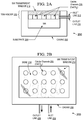
- FIGs. 2A and 2B illustrate a cross-sectional view and a top view, respectively, of an example nanofluidic device 200.
- the device 200 includes a TEM holder 202 that holds a silicon substrate 204 and calcite channels 206.
- the calcite deposits that make up the channels 206 can have any shape, such as a cylinder or a cuboid.
- the pattern of the calcite channels 206 can be varied.
- the channels 206 can have a stacked row pattern, where the center of each calcite deposit is in line with a center of a calcite deposit in a row directly above or a row directly below, as illustrated in FIG. 2B .
- the channels 206 can have a shifted row pattern, where the center of each calcite deposit is not in line with a center of any calcite deposit in a row directly above or a row directly below.
- the straight or curved edges of the calcite deposits and the channel pattern can represent a variety of geometries that occur in natural calcite reservoirs.
- the calcite channels 206 of the nanofluidic device 200 can have a length in a range of 50 to 100 nm in at least one dimension.
- the width of each calcite channel 206 can be in the range of 50 to 100 nm.
- the silicon substrate 204 and the calcite channels 206 can be packaged in a casing 208 with a window 210 transparent to an electron beam on top of the calcite channels 206.
- the casing 208 can be made of a conductive metal
- the window 210 can be made of an electrically conductive material that is also optically transparent, such as silicon nitride (SiN). Electrical conductivity allows the window 210 to avoid accumulating an electric charge, and the transparency of the window 210 allows observation.
- the casing has an inlet line 212 that allows a fluid, such as brine solution 214, to enter the nanofluidic device 200 and an outlet line 216 that allows fluid to exit.
- the inlet line 212 and outlet line 216 can be located on the same side of the device 200. In some implementations, the inlet line 212 and outlet line 216 can be located on opposite or adjacent sides of the device 200.
- FIG. 3 illustrates an example system 300 for testing a nanofluidic device 200.
- the system 300 can image a reaction between the calcite channels 206 and a fluid.
- the nanofluidic device 200 is positioned on a sample stage located inside a TEM chamber 322.
- the TEM chamber 322 can isolate the device 200 from outside interference and can be evacuated-that is, a vacuum can be produced within the chamber.
- Fluid such as brine solution, can be introduced, by way of a TEM holder 328, to the device by inlet line 212, and the fluid can exit by outlet line 216.
- an electron beam gun 320 emits an electron beam to produce a projected image 326 of the calcite channels 206 while interacting with the fluid.
- the electron beam gun 320, the TEM chamber 322, and sample stage can be components of a single apparatus, such as an SEM.
- the electron beam gun 320 is the same source of electrons used to perform electron beam lithography in fabricating the nanofluidic device 200, for example, a modified SEM capable of performing electron beam lithography.
- Calcite reservoirs are typically heterogeneous. Some areas of the reservoir can contain large voids, whereas other areas can have poor connectivity and low permeability. Acid injection is an enhanced oil recovery method that can increase the connectivity of an area of a reservoir. Acid injection can include a brine solution 214 with acid content, for example 10% hydrochloric acid. Acid injection causes carbonate dissolution, and the dynamics of formation dissolution due to acid flow on a pore-scale and an atomic-scale can determine the net flow behavior. The dynamics can also determine other reservoir characteristics such as likelihood for leakage, oil and gas recovery, and storage capacity. As brine solution 214 flows through the nanofluidic device 200, the SEM can be utilized to observe calcite dissolution and preferential flow of brine at a nanometer scale in the device 200. The observations can then be used to quantify acid dissolution of carbonates and to predict the migration of brine through aquifers, such as calcite formations.
- FIG. 4 is a representation of an example of an image 400 that be produced by the system 300. Locations in FIG. 4 of the calcite channels 206 and the brine 214 are based on the locations of the calcite channels 206 and the brine 214 in FIG. 2B . A user reviewing the image 400 can learn information, for example, about the interactions between fluid-fluid and fluid-calcite rock interactions at an atomic scale.
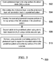
- FIG. 5 is a flowchart illustrating an example method 500 for fabricating a SiN substrate.
- the size and shape of the substrate can be determined, for example, by a sample stage of an SEM.
- a nanofluidic device containing the SiN substrate can be packaged, and the size of the substrate can be smaller than a size of a hole in the TEM holder.
- substrate preparation can include cleaning of the substrate.
- a top surface of a silicon nitride (SiN) substrate is coated with a photoresist layer.
- coating the photoresist layer can use an epoxy-based negative photoresist layer that is spin-coated on the surface of the SiN substrate.
- the epoxy-based negative photoresist is polydimethylsiloxane (PDMS) or SU-8.
- PDMS polydimethylsiloxane
- a number of parameters can determine the thickness of the coated layer of photoresist such as a spin rate, a photoresist viscosity, a temperature, and other parameters. In some implementations, the thickness can equal a desired height of calcite channels in a nanofluidic device.
- Forming channel patterns can involve, for example, exposing a portion of the photoresist to a beam of electrons from an SEM.
- a beam of electrons can be supplied by a scanning electron microscope.
- the exposure of the resist can be followed by a post-exposure baking step that includes, for example, baking at approximately 200°F for a duration of time, which is dependent on the thickness of the layer of the photoresist.
- the scanned photoresist is developed to expose portions of the top surface of the SiN substrate in the predefined pattern.
- the exposed portion of the photoresist is developed, that is, removed.
- Developing the photoresist involves dissolving the photoresist using a solvent, such as PGMEA, ethyl lactate, or di-acetone alcohol.
- Developing the photoresist also involves revealing a portion of surface of the substrate.
- calcite is deposited in the predefined pattern using atomic layer deposition (ALD) using a calcite precursor gas.
- ALD atomic layer deposition
- calcite precursor gas For example, after the patterns are drawn and etched, the etched hollow patterns can be filled with calcite by using ALD with a calcite precursor gas.
- Calcite is deposited in the channel patterns using atomic layer deposition with calcite precursor gas.
- Atomic layer deposition involves depositing calcite, layer by layer. In certain implementations, calcite is deposited layer by layer until the calcite channel height is similar to or the same as the original height of the coated photoresist at 504.
- a remaining portion of the photoresist layer is removed to expose the deposited calcite in the predefined pattern and on the top surface of the SiN substrate.
- the calcite channel structure is deposited on the substrate and the substrate remain.
- the formed calcite channels can have a length in a range of 50 to 100 nm in at least one dimension.
- the casing can include a top portion with a window, a bottom portion that can hold the device, an inlet connection to allow a fluid to enter the device, and an outlet connection to allow the fluid to exit the device.
- the window can be made of an electrically conductive and optically transparent material, such as SiN, and can be set on top of the calcite channels deposited on the substrate.
- the package includes a metal casing around the substrate.
- method 500 further includes steps for injecting, imaging, and removing a sample.
- the sample can be, for example, a liquid or a liquid containing nanoparticles.
- the SiN substrate can be inserted into a liquid cell TEM holder having an inlet and an outlet. Then, a sample can be deposited onto the SiN substrate and the deposited calcite, and the chip can be sealed with a window on the TEM holder.
- the window includes an electrically conductive and optically transparent SiN window.
- the chip can be imaged using a TEM while injecting the sample through the inlet, and the sample can be removed through the outlet.
- method 500 can be implemented using one or more computers.
- computers can be used to automate a machine or other equipment to perform some or all of the steps of method 500.
- Described implementations of the subject matter can include one or more features, alone or in combination.
- a method includes the following steps.
- a photoresist layer is coated onto a top surface of a SiN substrate.
- the photoresist layer is scanned with an electron beam in a predefined pattern.
- the scanned photoresist is developed to expose portions of the top surface of the SiN substrate in the predefined pattern.
- Calcite is deposited in the predefined pattern using ALD using a calcite precursor gas.
- a solvent a remaining portion of the photoresist layer is removed to expose the deposited calcite in the predefined pattern and on the top surface of the SiN substrate, where a width of the deposited calcite is in range from 50 to 100 nm.
- a system in a second implementation, includes a nanofluidic device, a casing for the device; and an electron source for providing a beam of electrons.
- the device includes a bottom portion that includes a substrate and a top portion that includes a calcite channel structure.
- the calcite channel structure includes at least one side having a length in a range of approximately 50 to 100 nanometers.
Landscapes
- Physics & Mathematics (AREA)
- General Physics & Mathematics (AREA)
- Chemical & Material Sciences (AREA)
- Engineering & Computer Science (AREA)
- Spectroscopy & Molecular Physics (AREA)
- Manufacturing & Machinery (AREA)
- Organic Chemistry (AREA)
- Mechanical Engineering (AREA)
- Metallurgy (AREA)
- General Chemical & Material Sciences (AREA)
- Chemical Kinetics & Catalysis (AREA)
- Materials Engineering (AREA)
- Health & Medical Sciences (AREA)
- Toxicology (AREA)
- Microelectronics & Electronic Packaging (AREA)
- Analytical Chemistry (AREA)
- Dispersion Chemistry (AREA)
- Analysing Materials By The Use Of Radiation (AREA)
- Life Sciences & Earth Sciences (AREA)
- Geology (AREA)
- Inorganic Chemistry (AREA)
- Formation Of Insulating Films (AREA)
- Chemical Vapour Deposition (AREA)
Claims (14)
- Verfahren, umfassend:Aufbringen (502) einer Photoresistschicht als Beschichtung auf eine Deckfläche eines Siliciumnitridsubstrats;nach dem Aufbringen der Photoresistschicht als Beschichtung Scannen (504) der Photoresistschicht mit einem Elektronenstrahl in einem vordefinierten Muster;Entwickeln (506) des gescannten Photoresists, um Anteile der Deckfläche des Siliciumnitridsubstrats in dem vordefinierten Muster zu exponieren;Abscheiden (508) von Calcit in dem vordefinierten Muster unter Verwendung von Atomlagenabscheidung unter Verwendung eines Calcitvorläufergases; undEntfernen (510) eines verbleibenden Anteils der Photoresistschicht unter Verwendung eines Lösungsmittels, um das abgeschiedene Calcit in dem vordefinierten Muster und auf der Deckfläche des Siliciumnitridsubstrats zu exponieren, wobei eine Breite des abgeschiedenen Calcits im Bereich von 50 bis 100 Nanometern liegt.
- Verfahren nach Anspruch 1, des Weiteren umfassend:Einsetzen des Siliciumnitridsubstrats in einen Flüssigzellenhalter für Transmissionselektronenmikroskopie, der einen Einlass und einen Auslass aufweist;Abscheiden einer Probe auf dem Siliciumnitridsubstrat und dem abgeschiedenen Calcit;Versiegeln des Chips mit einem Fenster auf dem Halter für Transmissionselektronenmikroskopie; undAbbilden des Chips unter Verwendung von Transmissionselektronenmikroskopie, während die Probe durch den Einlass injiziert wird und die Probe durch den Auslass entfernt wird.
- Verfahren nach Anspruch 2, wobei eine Größe des Siliciumnitridsubstrats von einer Größe eines Loches in dem Halter für Transmissionselektronenmikroskopie abhängt und kleiner als diese ist.
- Verfahren nach Anspruch 1, wobei Aufbringen der Photoresistschicht durch Beschichten eine Negativphotoresistschicht auf Epoxybasis verwendet, die mittels Rotationsbeschichten auf die Oberfläche des Siliciumnitridsubstrats aufgebracht wird.
- Verfahren nach Anspruch 4, wobei der Negativphotoresist auf Epoxybasis Polydimethylsiloxan oder SU-8 ist.
- Verfahren nach Anspruch 1, wobei die Probe eine Flüssigkeit oder eine Nanopartikel enthaltende Flüssigkeit ist.
- Verfahren nach Anspruch 1, wobei das Lösungsmittel Propylenglykolmethyletheracetat, Ethyllactat oder Diacetonalkohol umfasst.
- Verfahren nach Anspruch 1, wobei das Fenster ein elektrisch leitfähiges und optisch transparentes Siliciumnitridfenster umfasst.
- System, umfassend:eine nanofluidische Vorrichtung (200), wobei die Vorrichtung einen unteren Anteil, der ein Substrat (204) umfasst, und einen oberen Anteil umfasst, der eine Calcitkanal- (206)-Struktur umfasst, wobei die Calcitkanalstruktur mindestens eine Seite mit einer Länge in einem Bereich von annähernd 50 bis 100 Nanometern umfasst;ein Gehäuse (208) für die Vorrichtung; undeine Elektronenquelle zur Bereitstellung eines Strahls von Elektronen.
- System nach Anspruch 9, wobei das Substrat Silicium umfasst.
- System nach Anspruch 9, wobei die Elektronenquelle ein Rasterelektronenmikroskop ist.
- Verfahren nach Anspruch 9, wobei das Gehäuse umfasst:einen oberen Anteil, der ein Fenster (210) umfasst;einen unteren Anteil, der ausgestaltet ist, um die Vorrichtung zu halten;eine Einlassleitung (212), die ausgestaltet ist, um zuzulassen, dass ein Fluid in die Vorrichtung eintritt; undeine Auslassleitung (216), die ausgestaltet ist, um zuzulassen, dass ein Fluid aus der Vorrichtung austritt.
- System nach Anspruch 9, wobei das Fenster ein elektrisch leitfähiges und optisch transparentes Material umfasst.
- System nach Anspruch 13, wobei das elektrisch leitfähige und optisch transparente Material Siliciumnitrid umfasst.
Applications Claiming Priority (2)
| Application Number | Priority Date | Filing Date | Title |
|---|---|---|---|
| US16/114,906 US10761428B2 (en) | 2018-08-28 | 2018-08-28 | Fabricating calcite nanofluidic channels |
| PCT/US2019/048322 WO2020046918A1 (en) | 2018-08-28 | 2019-08-27 | Fabricating calcite nanofluidic channels |
Publications (2)
| Publication Number | Publication Date |
|---|---|
| EP3844568A1 EP3844568A1 (de) | 2021-07-07 |
| EP3844568B1 true EP3844568B1 (de) | 2021-11-24 |
Family
ID=67902655
Family Applications (1)
| Application Number | Title | Priority Date | Filing Date |
|---|---|---|---|
| EP19765910.5A Active EP3844568B1 (de) | 2018-08-28 | 2019-08-27 | Herstellung von calcit-nanofluidischen kanälen |
Country Status (6)
| Country | Link |
|---|---|
| US (2) | US10761428B2 (de) |
| EP (1) | EP3844568B1 (de) |
| CN (1) | CN112639619A (de) |
| CA (1) | CA3116609C (de) |
| SA (1) | SA521421323B1 (de) |
| WO (1) | WO2020046918A1 (de) |
Families Citing this family (7)
| Publication number | Priority date | Publication date | Assignee | Title |
|---|---|---|---|---|
| US10926227B2 (en) * | 2018-12-03 | 2021-02-23 | Saudi Arabian Oil Company | Fabricating calcite nanofluidic channels |
| US11961702B2 (en) | 2021-12-09 | 2024-04-16 | Saudi Arabian Oil Company | Fabrication of in situ HR-LCTEM nanofluidic cell for nanobubble interactions during EOR processes in carbonate rocks |
| US11787993B1 (en) | 2022-03-28 | 2023-10-17 | Saudi Arabian Oil Company | In-situ foamed gel for lost circulation |
| US20230330658A1 (en) * | 2022-04-18 | 2023-10-19 | Saudi Arabian Oil Company | Calcite coated microfluidic cell and methods thereof |
| US11913319B2 (en) | 2022-06-21 | 2024-02-27 | Saudi Arabian Oil Company | Sandstone stimulation |
| US20250087443A1 (en) * | 2023-09-07 | 2025-03-13 | Saudi Arabian Oil Company | Nanofluidic cell for characterization of nano-bubbles in a simulated reservoir |
| US20250354246A1 (en) * | 2024-05-14 | 2025-11-20 | Saudi Arabian Oil Company | Calcite channel nanofluidics |
Family Cites Families (35)
| Publication number | Priority date | Publication date | Assignee | Title |
|---|---|---|---|---|
| FR2280435A1 (fr) | 1974-08-02 | 1976-02-27 | Rhone Poulenc Ind | Procede d'obtention d'une membrane microporeuse et nouveau produit ainsi obtenu |
| US4564997A (en) | 1981-04-21 | 1986-01-21 | Nippon-Telegraph And Telephone Public Corporation | Semiconductor device and manufacturing process thereof |
| JPH0647482Y2 (ja) | 1991-09-06 | 1994-12-07 | 楊 淨雅 | 複数のゲームのための駒の組合せユニット |
| US6908770B1 (en) * | 1998-07-16 | 2005-06-21 | Board Of Regents, The University Of Texas System | Fluid based analysis of multiple analytes by a sensor array |
| US6610605B2 (en) | 2001-06-28 | 2003-08-26 | Intel Corporation | Method and apparatus for fabricating encapsulated micro-channels in a substrate |
| US7279134B2 (en) | 2002-09-17 | 2007-10-09 | Intel Corporation | Microfluidic devices with porous membranes for molecular sieving, metering, and separations |
| CN101831163B (zh) * | 2002-11-01 | 2013-07-10 | 佐治亚技术研究公司 | 牺牲组合物、其应用以及分解方法 |
| JP4454931B2 (ja) | 2002-12-13 | 2010-04-21 | キヤノン株式会社 | ドットパターンを有する基板の製造方法及び柱状構造体の製造方法 |
| ITTO20030167A1 (it) | 2003-03-06 | 2004-09-07 | Fiat Ricerche | Procedimento per la realizzazione di emettitori nano-strutturati per sorgenti di luce ad incandescenza. |
| EP1831763A1 (de) * | 2004-12-20 | 2007-09-12 | Koninklijke Philips Electronics N.V. | Oberflächenmustererzeugung und herstellung von bohrungen unter verwendung von kontrolliertem ablagerungswachstum |
| ITTO20050478A1 (it) | 2005-07-12 | 2007-01-13 | St Microelectronics Srl | Procedimento per la realizzazione di cavita' sepolte all'interno di un corpo semiconduttore e corpo semiconduttore cosi' realizzato |
| US20070277866A1 (en) | 2006-05-31 | 2007-12-06 | General Electric Company | Thermoelectric nanotube arrays |
| GB0702560D0 (en) | 2007-02-09 | 2007-03-21 | Univ Bath | Production of Semiconductor devices |
| TWI376816B (en) | 2007-04-04 | 2012-11-11 | Epistar Corp | Electronic component assembly with composite material carrier |
| US7862986B2 (en) | 2007-10-17 | 2011-01-04 | Macronix International Co., Ltd. | Patterning process |
| JP2009134255A (ja) | 2007-10-31 | 2009-06-18 | Sekisui Chem Co Ltd | マイクロパターン形成用材料、マイクロパターン複合材及びその製造方法並びに微小3次元構造基板の製造方法 |
| WO2009061823A1 (en) | 2007-11-05 | 2009-05-14 | Trustees Of Tufts College | Fabrication of silk fibroin photonic structures by nanocontact imprinting |
| CA2727095C (en) | 2008-06-06 | 2020-01-07 | Bionano Genomics, Inc. | Integrated analysis devices and related fabrication methods and analysis techniques |
| US8435415B2 (en) | 2009-11-24 | 2013-05-07 | The United States of America, as represented by the Secretary of Commerce, The National Institute of Standards and Technology | Nanofabrication process and nanodevice |
| CN103081107B (zh) | 2010-03-09 | 2017-02-08 | 得克萨斯州大学系统董事会 | 多孔和非多孔纳米结构 |
| WO2012017197A1 (en) | 2010-08-06 | 2012-02-09 | Bp Exploration Operating Company Limited | Apparatus and method for testing multiple samples |
| WO2012048040A2 (en) | 2010-10-05 | 2012-04-12 | Anpac Bio-Medical Science Co., Ltd. | Micro-devices for disease detection |
| US9207196B2 (en) * | 2010-11-17 | 2015-12-08 | Vanderbilt University | Transmission electron microscopy for imaging live cells |
| WO2012137847A1 (ja) | 2011-04-05 | 2012-10-11 | ダブル・スコープ株式会社 | 多孔性膜およびその製造方法 |
| KR101209151B1 (ko) | 2011-04-25 | 2012-12-06 | 광주과학기술원 | 양자점 제조방법 및 양자점을 포함하는 반도체 구조물 |
| CN103297565B (zh) | 2012-02-24 | 2015-07-22 | 比亚迪股份有限公司 | 一种手机壳体及其制备方法 |
| US11493428B2 (en) * | 2013-03-15 | 2022-11-08 | Gpb Scientific, Inc. | On-chip microfluidic processing of particles |
| JP2016524156A (ja) | 2013-06-26 | 2016-08-12 | ユニヴァーシティ オブ ワシントン センター フォー コマーシャライゼーション | 個別化された凝集測定のための流体素子 |
| JP6807752B2 (ja) | 2014-06-03 | 2021-01-06 | ザ ケマーズ カンパニー エフシー リミテッド ライアビリティ カンパニー | 光架橋フルオロポリマーを含む保護層 |
| KR20160014504A (ko) | 2014-07-29 | 2016-02-11 | 광주과학기술원 | 패럴린 박막을 포함하는 미세유체소자의 제조방법 및 이에 의해 제조된 미세유체소자 |
| US10722888B2 (en) | 2015-07-16 | 2020-07-28 | The Hong Kong University Of Science And Technology | Dynamic formation of nanochannels for single-molecule DNA analysis |
| EP3130559A1 (de) | 2015-08-14 | 2017-02-15 | Max-Planck-Gesellschaft zur Förderung der Wissenschaften e.V. | Herstellung von nanostrukturierten substraten mit mehreren nanostrukturgradienten auf einem einzelnen substrat |
| US9869649B2 (en) | 2015-09-03 | 2018-01-16 | Saudi Arabian Oil Company | Nano-level evaluation of kerogen-rich reservoir rock |
| US10365564B2 (en) * | 2017-08-09 | 2019-07-30 | Saudi Arabian Oil Company | Calcite channel nanofluidics |
| US10926227B2 (en) | 2018-12-03 | 2021-02-23 | Saudi Arabian Oil Company | Fabricating calcite nanofluidic channels |
-
2018
- 2018-08-28 US US16/114,906 patent/US10761428B2/en active Active
-
2019
- 2019-08-27 CN CN201980056054.0A patent/CN112639619A/zh active Pending
- 2019-08-27 CA CA3116609A patent/CA3116609C/en active Active
- 2019-08-27 WO PCT/US2019/048322 patent/WO2020046918A1/en not_active Ceased
- 2019-08-27 EP EP19765910.5A patent/EP3844568B1/de active Active
-
2020
- 2020-06-11 US US16/898,718 patent/US11366391B2/en active Active
-
2021
- 2021-02-24 SA SA521421323A patent/SA521421323B1/ar unknown
Also Published As
| Publication number | Publication date |
|---|---|
| CN112639619A (zh) | 2021-04-09 |
| US20200071824A1 (en) | 2020-03-05 |
| WO2020046918A1 (en) | 2020-03-05 |
| US11366391B2 (en) | 2022-06-21 |
| CA3116609C (en) | 2021-10-26 |
| EP3844568A1 (de) | 2021-07-07 |
| US10761428B2 (en) | 2020-09-01 |
| CA3116609A1 (en) | 2020-03-05 |
| SA521421323B1 (ar) | 2022-08-24 |
| US20200301282A1 (en) | 2020-09-24 |
Similar Documents
| Publication | Publication Date | Title |
|---|---|---|
| EP3844568B1 (de) | Herstellung von calcit-nanofluidischen kanälen | |
| EP3665532B1 (de) | Calcitkanal-nanofluidik | |
| KR101906613B1 (ko) | 액체에서 초소수성을 회복하고 유지하기 위한 방법 및 장치 | |
| US9086621B2 (en) | Methods for providing spaced lithography features on a substrate by self-assembly of block copolymers | |
| US8828253B2 (en) | Lithography using self-assembled polymers | |
| US11628406B2 (en) | Fabricating calcite nanofluidic channels | |
| AlOmier et al. | Novel fabrication of mixed wettability micromodels for pore-scale studies of fluid–rock interactions | |
| US20220107302A1 (en) | Calcite channel structures with heterogeneous wettability | |
| US20250354246A1 (en) | Calcite channel nanofluidics | |
| da Silva et al. | Fabrication of a hybrid device for the integration of light-triggered proton pumps | |
| US20230187170A1 (en) | Fabrication of in situ hr-lctem nanofluidic cell for nanobubble interactions during eor processes in carbonate rocks | |
| EP2756167A2 (de) | Nanostrukturierte flüssigkeitsprobenahmevorrichtung | |
| Le-Anh et al. | Oil Displacement in Calcite-Coated Microfluidic Chips via Waterflooding at Elevated Temperatures and Long Times. Micromachines 2022, 13, 1316 | |
| da Silva et al. | Micro and Nano Engineering |
Legal Events
| Date | Code | Title | Description |
|---|---|---|---|
| STAA | Information on the status of an ep patent application or granted ep patent |
Free format text: STATUS: UNKNOWN |
|
| STAA | Information on the status of an ep patent application or granted ep patent |
Free format text: STATUS: THE INTERNATIONAL PUBLICATION HAS BEEN MADE |
|
| STAA | Information on the status of an ep patent application or granted ep patent |
Free format text: STATUS: REQUEST FOR EXAMINATION WAS MADE |
|
| PUAI | Public reference made under article 153(3) epc to a published international application that has entered the european phase |
Free format text: ORIGINAL CODE: 0009012 |
|
| 17P | Request for examination filed |
Effective date: 20210318 |
|
| AK | Designated contracting states |
Kind code of ref document: A1 Designated state(s): AL AT BE BG CH CY CZ DE DK EE ES FI FR GB GR HR HU IE IS IT LI LT LU LV MC MK MT NL NO PL PT RO RS SE SI SK SM TR |
|
| GRAP | Despatch of communication of intention to grant a patent |
Free format text: ORIGINAL CODE: EPIDOSNIGR1 |
|
| STAA | Information on the status of an ep patent application or granted ep patent |
Free format text: STATUS: GRANT OF PATENT IS INTENDED |
|
| INTG | Intention to grant announced |
Effective date: 20210809 |
|
| GRAS | Grant fee paid |
Free format text: ORIGINAL CODE: EPIDOSNIGR3 |
|
| GRAA | (expected) grant |
Free format text: ORIGINAL CODE: 0009210 |
|
| STAA | Information on the status of an ep patent application or granted ep patent |
Free format text: STATUS: THE PATENT HAS BEEN GRANTED |
|
| AK | Designated contracting states |
Kind code of ref document: B1 Designated state(s): AL AT BE BG CH CY CZ DE DK EE ES FI FR GB GR HR HU IE IS IT LI LT LU LV MC MK MT NL NO PL PT RO RS SE SI SK SM TR |
|
| DAV | Request for validation of the european patent (deleted) | ||
| DAX | Request for extension of the european patent (deleted) | ||
| REG | Reference to a national code |
Ref country code: GB Ref legal event code: FG4D |
|
| REG | Reference to a national code |
Ref country code: AT Ref legal event code: REF Ref document number: 1450306 Country of ref document: AT Kind code of ref document: T Effective date: 20211215 |
|
| REG | Reference to a national code |
Ref country code: DE Ref legal event code: R096 Ref document number: 602019009565 Country of ref document: DE |
|
| REG | Reference to a national code |
Ref country code: IE Ref legal event code: FG4D |
|
| REG | Reference to a national code |
Ref country code: LT Ref legal event code: MG9D |
|
| REG | Reference to a national code |
Ref country code: NL Ref legal event code: MP Effective date: 20211124 |
|
| REG | Reference to a national code |
Ref country code: AT Ref legal event code: MK05 Ref document number: 1450306 Country of ref document: AT Kind code of ref document: T Effective date: 20211124 |
|
| PG25 | Lapsed in a contracting state [announced via postgrant information from national office to epo] |
Ref country code: RS Free format text: LAPSE BECAUSE OF FAILURE TO SUBMIT A TRANSLATION OF THE DESCRIPTION OR TO PAY THE FEE WITHIN THE PRESCRIBED TIME-LIMIT Effective date: 20211124 Ref country code: LT Free format text: LAPSE BECAUSE OF FAILURE TO SUBMIT A TRANSLATION OF THE DESCRIPTION OR TO PAY THE FEE WITHIN THE PRESCRIBED TIME-LIMIT Effective date: 20211124 Ref country code: FI Free format text: LAPSE BECAUSE OF FAILURE TO SUBMIT A TRANSLATION OF THE DESCRIPTION OR TO PAY THE FEE WITHIN THE PRESCRIBED TIME-LIMIT Effective date: 20211124 Ref country code: BG Free format text: LAPSE BECAUSE OF FAILURE TO SUBMIT A TRANSLATION OF THE DESCRIPTION OR TO PAY THE FEE WITHIN THE PRESCRIBED TIME-LIMIT Effective date: 20220224 Ref country code: AT Free format text: LAPSE BECAUSE OF FAILURE TO SUBMIT A TRANSLATION OF THE DESCRIPTION OR TO PAY THE FEE WITHIN THE PRESCRIBED TIME-LIMIT Effective date: 20211124 |
|
| PG25 | Lapsed in a contracting state [announced via postgrant information from national office to epo] |
Ref country code: IS Free format text: LAPSE BECAUSE OF FAILURE TO SUBMIT A TRANSLATION OF THE DESCRIPTION OR TO PAY THE FEE WITHIN THE PRESCRIBED TIME-LIMIT Effective date: 20220324 Ref country code: SE Free format text: LAPSE BECAUSE OF FAILURE TO SUBMIT A TRANSLATION OF THE DESCRIPTION OR TO PAY THE FEE WITHIN THE PRESCRIBED TIME-LIMIT Effective date: 20211124 Ref country code: PT Free format text: LAPSE BECAUSE OF FAILURE TO SUBMIT A TRANSLATION OF THE DESCRIPTION OR TO PAY THE FEE WITHIN THE PRESCRIBED TIME-LIMIT Effective date: 20220324 Ref country code: PL Free format text: LAPSE BECAUSE OF FAILURE TO SUBMIT A TRANSLATION OF THE DESCRIPTION OR TO PAY THE FEE WITHIN THE PRESCRIBED TIME-LIMIT Effective date: 20211124 Ref country code: NO Free format text: LAPSE BECAUSE OF FAILURE TO SUBMIT A TRANSLATION OF THE DESCRIPTION OR TO PAY THE FEE WITHIN THE PRESCRIBED TIME-LIMIT Effective date: 20220224 Ref country code: NL Free format text: LAPSE BECAUSE OF FAILURE TO SUBMIT A TRANSLATION OF THE DESCRIPTION OR TO PAY THE FEE WITHIN THE PRESCRIBED TIME-LIMIT Effective date: 20211124 Ref country code: LV Free format text: LAPSE BECAUSE OF FAILURE TO SUBMIT A TRANSLATION OF THE DESCRIPTION OR TO PAY THE FEE WITHIN THE PRESCRIBED TIME-LIMIT Effective date: 20211124 Ref country code: HR Free format text: LAPSE BECAUSE OF FAILURE TO SUBMIT A TRANSLATION OF THE DESCRIPTION OR TO PAY THE FEE WITHIN THE PRESCRIBED TIME-LIMIT Effective date: 20211124 Ref country code: GR Free format text: LAPSE BECAUSE OF FAILURE TO SUBMIT A TRANSLATION OF THE DESCRIPTION OR TO PAY THE FEE WITHIN THE PRESCRIBED TIME-LIMIT Effective date: 20220225 |
|
| PG25 | Lapsed in a contracting state [announced via postgrant information from national office to epo] |
Ref country code: SM Free format text: LAPSE BECAUSE OF FAILURE TO SUBMIT A TRANSLATION OF THE DESCRIPTION OR TO PAY THE FEE WITHIN THE PRESCRIBED TIME-LIMIT Effective date: 20211124 Ref country code: SK Free format text: LAPSE BECAUSE OF FAILURE TO SUBMIT A TRANSLATION OF THE DESCRIPTION OR TO PAY THE FEE WITHIN THE PRESCRIBED TIME-LIMIT Effective date: 20211124 Ref country code: RO Free format text: LAPSE BECAUSE OF FAILURE TO SUBMIT A TRANSLATION OF THE DESCRIPTION OR TO PAY THE FEE WITHIN THE PRESCRIBED TIME-LIMIT Effective date: 20211124 Ref country code: ES Free format text: LAPSE BECAUSE OF FAILURE TO SUBMIT A TRANSLATION OF THE DESCRIPTION OR TO PAY THE FEE WITHIN THE PRESCRIBED TIME-LIMIT Effective date: 20211124 Ref country code: EE Free format text: LAPSE BECAUSE OF FAILURE TO SUBMIT A TRANSLATION OF THE DESCRIPTION OR TO PAY THE FEE WITHIN THE PRESCRIBED TIME-LIMIT Effective date: 20211124 Ref country code: DK Free format text: LAPSE BECAUSE OF FAILURE TO SUBMIT A TRANSLATION OF THE DESCRIPTION OR TO PAY THE FEE WITHIN THE PRESCRIBED TIME-LIMIT Effective date: 20211124 Ref country code: CZ Free format text: LAPSE BECAUSE OF FAILURE TO SUBMIT A TRANSLATION OF THE DESCRIPTION OR TO PAY THE FEE WITHIN THE PRESCRIBED TIME-LIMIT Effective date: 20211124 |
|
| REG | Reference to a national code |
Ref country code: DE Ref legal event code: R097 Ref document number: 602019009565 Country of ref document: DE |
|
| PLBE | No opposition filed within time limit |
Free format text: ORIGINAL CODE: 0009261 |
|
| STAA | Information on the status of an ep patent application or granted ep patent |
Free format text: STATUS: NO OPPOSITION FILED WITHIN TIME LIMIT |
|
| PG25 | Lapsed in a contracting state [announced via postgrant information from national office to epo] |
Ref country code: AL Free format text: LAPSE BECAUSE OF FAILURE TO SUBMIT A TRANSLATION OF THE DESCRIPTION OR TO PAY THE FEE WITHIN THE PRESCRIBED TIME-LIMIT Effective date: 20211124 |
|
| 26N | No opposition filed |
Effective date: 20220825 |
|
| REG | Reference to a national code |
Ref country code: DE Ref legal event code: R119 Ref document number: 602019009565 Country of ref document: DE |
|
| PG25 | Lapsed in a contracting state [announced via postgrant information from national office to epo] |
Ref country code: MC Free format text: LAPSE BECAUSE OF FAILURE TO SUBMIT A TRANSLATION OF THE DESCRIPTION OR TO PAY THE FEE WITHIN THE PRESCRIBED TIME-LIMIT Effective date: 20211124 |
|
| REG | Reference to a national code |
Ref country code: CH Ref legal event code: PL |
|
| PG25 | Lapsed in a contracting state [announced via postgrant information from national office to epo] |
Ref country code: LU Free format text: LAPSE BECAUSE OF NON-PAYMENT OF DUE FEES Effective date: 20220827 Ref country code: LI Free format text: LAPSE BECAUSE OF NON-PAYMENT OF DUE FEES Effective date: 20220831 Ref country code: CH Free format text: LAPSE BECAUSE OF NON-PAYMENT OF DUE FEES Effective date: 20220831 |
|
| REG | Reference to a national code |
Ref country code: BE Ref legal event code: MM Effective date: 20220831 |
|
| PG25 | Lapsed in a contracting state [announced via postgrant information from national office to epo] |
Ref country code: IT Free format text: LAPSE BECAUSE OF FAILURE TO SUBMIT A TRANSLATION OF THE DESCRIPTION OR TO PAY THE FEE WITHIN THE PRESCRIBED TIME-LIMIT Effective date: 20211124 |
|
| P01 | Opt-out of the competence of the unified patent court (upc) registered |
Effective date: 20230528 |
|
| PG25 | Lapsed in a contracting state [announced via postgrant information from national office to epo] |
Ref country code: IE Free format text: LAPSE BECAUSE OF NON-PAYMENT OF DUE FEES Effective date: 20220827 Ref country code: FR Free format text: LAPSE BECAUSE OF NON-PAYMENT OF DUE FEES Effective date: 20220831 Ref country code: DE Free format text: LAPSE BECAUSE OF NON-PAYMENT OF DUE FEES Effective date: 20230301 |
|
| PG25 | Lapsed in a contracting state [announced via postgrant information from national office to epo] |
Ref country code: BE Free format text: LAPSE BECAUSE OF NON-PAYMENT OF DUE FEES Effective date: 20220831 |
|
| PG25 | Lapsed in a contracting state [announced via postgrant information from national office to epo] |
Ref country code: CY Free format text: LAPSE BECAUSE OF FAILURE TO SUBMIT A TRANSLATION OF THE DESCRIPTION OR TO PAY THE FEE WITHIN THE PRESCRIBED TIME-LIMIT Effective date: 20211124 |
|
| PG25 | Lapsed in a contracting state [announced via postgrant information from national office to epo] |
Ref country code: MK Free format text: LAPSE BECAUSE OF FAILURE TO SUBMIT A TRANSLATION OF THE DESCRIPTION OR TO PAY THE FEE WITHIN THE PRESCRIBED TIME-LIMIT Effective date: 20211124 Ref country code: HU Free format text: LAPSE BECAUSE OF FAILURE TO SUBMIT A TRANSLATION OF THE DESCRIPTION OR TO PAY THE FEE WITHIN THE PRESCRIBED TIME-LIMIT; INVALID AB INITIO Effective date: 20190827 |
|
| PG25 | Lapsed in a contracting state [announced via postgrant information from national office to epo] |
Ref country code: TR Free format text: LAPSE BECAUSE OF FAILURE TO SUBMIT A TRANSLATION OF THE DESCRIPTION OR TO PAY THE FEE WITHIN THE PRESCRIBED TIME-LIMIT Effective date: 20211124 |
|
| PG25 | Lapsed in a contracting state [announced via postgrant information from national office to epo] |
Ref country code: MT Free format text: LAPSE BECAUSE OF FAILURE TO SUBMIT A TRANSLATION OF THE DESCRIPTION OR TO PAY THE FEE WITHIN THE PRESCRIBED TIME-LIMIT Effective date: 20211124 |
|
| PGFP | Annual fee paid to national office [announced via postgrant information from national office to epo] |
Ref country code: GB Payment date: 20250828 Year of fee payment: 7 |
|
| PG25 | Lapsed in a contracting state [announced via postgrant information from national office to epo] |
Ref country code: SI Free format text: LAPSE BECAUSE OF FAILURE TO SUBMIT A TRANSLATION OF THE DESCRIPTION OR TO PAY THE FEE WITHIN THE PRESCRIBED TIME-LIMIT Effective date: 20211124 |