EP3839617B1 - Flüssigkristall-anzeigevorrichtung - Google Patents
Flüssigkristall-anzeigevorrichtung Download PDFInfo
- Publication number
- EP3839617B1 EP3839617B1 EP19217221.1A EP19217221A EP3839617B1 EP 3839617 B1 EP3839617 B1 EP 3839617B1 EP 19217221 A EP19217221 A EP 19217221A EP 3839617 B1 EP3839617 B1 EP 3839617B1
- Authority
- EP
- European Patent Office
- Prior art keywords
- display device
- decorative pattern
- substrate
- polarizer
- liquid crystal
- Prior art date
- Legal status (The legal status is an assumption and is not a legal conclusion. Google has not performed a legal analysis and makes no representation as to the accuracy of the status listed.)
- Active
Links
Images
Classifications
-
- G—PHYSICS
- G02—OPTICS
- G02F—OPTICAL DEVICES OR ARRANGEMENTS FOR THE CONTROL OF LIGHT BY MODIFICATION OF THE OPTICAL PROPERTIES OF THE MEDIA OF THE ELEMENTS INVOLVED THEREIN; NON-LINEAR OPTICS; FREQUENCY-CHANGING OF LIGHT; OPTICAL LOGIC ELEMENTS; OPTICAL ANALOGUE/DIGITAL CONVERTERS
- G02F1/00—Devices or arrangements for the control of the intensity, colour, phase, polarisation or direction of light arriving from an independent light source, e.g. switching, gating or modulating; Non-linear optics
- G02F1/01—Devices or arrangements for the control of the intensity, colour, phase, polarisation or direction of light arriving from an independent light source, e.g. switching, gating or modulating; Non-linear optics for the control of the intensity, phase, polarisation or colour
- G02F1/13—Devices or arrangements for the control of the intensity, colour, phase, polarisation or direction of light arriving from an independent light source, e.g. switching, gating or modulating; Non-linear optics for the control of the intensity, phase, polarisation or colour based on liquid crystals, e.g. single liquid crystal display cells
- G02F1/133—Constructional arrangements; Operation of liquid crystal cells; Circuit arrangements
- G02F1/1333—Constructional arrangements; Manufacturing methods
- G02F1/133308—Support structures for LCD panels, e.g. frames or bezels
-
- G—PHYSICS
- G02—OPTICS
- G02F—OPTICAL DEVICES OR ARRANGEMENTS FOR THE CONTROL OF LIGHT BY MODIFICATION OF THE OPTICAL PROPERTIES OF THE MEDIA OF THE ELEMENTS INVOLVED THEREIN; NON-LINEAR OPTICS; FREQUENCY-CHANGING OF LIGHT; OPTICAL LOGIC ELEMENTS; OPTICAL ANALOGUE/DIGITAL CONVERTERS
- G02F1/00—Devices or arrangements for the control of the intensity, colour, phase, polarisation or direction of light arriving from an independent light source, e.g. switching, gating or modulating; Non-linear optics
- G02F1/01—Devices or arrangements for the control of the intensity, colour, phase, polarisation or direction of light arriving from an independent light source, e.g. switching, gating or modulating; Non-linear optics for the control of the intensity, phase, polarisation or colour
- G02F1/13—Devices or arrangements for the control of the intensity, colour, phase, polarisation or direction of light arriving from an independent light source, e.g. switching, gating or modulating; Non-linear optics for the control of the intensity, phase, polarisation or colour based on liquid crystals, e.g. single liquid crystal display cells
- G02F1/133—Constructional arrangements; Operation of liquid crystal cells; Circuit arrangements
- G02F1/1333—Constructional arrangements; Manufacturing methods
- G02F1/1335—Structural association of cells with optical devices, e.g. polarisers or reflectors
- G02F1/133528—Polarisers
- G02F1/133536—Reflective polarizers
-
- G—PHYSICS
- G02—OPTICS
- G02F—OPTICAL DEVICES OR ARRANGEMENTS FOR THE CONTROL OF LIGHT BY MODIFICATION OF THE OPTICAL PROPERTIES OF THE MEDIA OF THE ELEMENTS INVOLVED THEREIN; NON-LINEAR OPTICS; FREQUENCY-CHANGING OF LIGHT; OPTICAL LOGIC ELEMENTS; OPTICAL ANALOGUE/DIGITAL CONVERTERS
- G02F1/00—Devices or arrangements for the control of the intensity, colour, phase, polarisation or direction of light arriving from an independent light source, e.g. switching, gating or modulating; Non-linear optics
- G02F1/01—Devices or arrangements for the control of the intensity, colour, phase, polarisation or direction of light arriving from an independent light source, e.g. switching, gating or modulating; Non-linear optics for the control of the intensity, phase, polarisation or colour
- G02F1/13—Devices or arrangements for the control of the intensity, colour, phase, polarisation or direction of light arriving from an independent light source, e.g. switching, gating or modulating; Non-linear optics for the control of the intensity, phase, polarisation or colour based on liquid crystals, e.g. single liquid crystal display cells
- G02F1/133—Constructional arrangements; Operation of liquid crystal cells; Circuit arrangements
- G02F1/1333—Constructional arrangements; Manufacturing methods
- G02F1/1335—Structural association of cells with optical devices, e.g. polarisers or reflectors
- G02F1/133553—Reflecting elements
-
- G—PHYSICS
- G02—OPTICS
- G02F—OPTICAL DEVICES OR ARRANGEMENTS FOR THE CONTROL OF LIGHT BY MODIFICATION OF THE OPTICAL PROPERTIES OF THE MEDIA OF THE ELEMENTS INVOLVED THEREIN; NON-LINEAR OPTICS; FREQUENCY-CHANGING OF LIGHT; OPTICAL LOGIC ELEMENTS; OPTICAL ANALOGUE/DIGITAL CONVERTERS
- G02F1/00—Devices or arrangements for the control of the intensity, colour, phase, polarisation or direction of light arriving from an independent light source, e.g. switching, gating or modulating; Non-linear optics
- G02F1/01—Devices or arrangements for the control of the intensity, colour, phase, polarisation or direction of light arriving from an independent light source, e.g. switching, gating or modulating; Non-linear optics for the control of the intensity, phase, polarisation or colour
- G02F1/13—Devices or arrangements for the control of the intensity, colour, phase, polarisation or direction of light arriving from an independent light source, e.g. switching, gating or modulating; Non-linear optics for the control of the intensity, phase, polarisation or colour based on liquid crystals, e.g. single liquid crystal display cells
- G02F1/133—Constructional arrangements; Operation of liquid crystal cells; Circuit arrangements
- G02F1/1333—Constructional arrangements; Manufacturing methods
- G02F1/1343—Electrodes
- G02F1/134309—Electrodes characterised by their geometrical arrangement
- G02F1/134327—Segmented, e.g. alpha numeric display
-
- G—PHYSICS
- G04—HOROLOGY
- G04B—MECHANICALLY-DRIVEN CLOCKS OR WATCHES; MECHANICAL PARTS OF CLOCKS OR WATCHES IN GENERAL; TIME PIECES USING THE POSITION OF THE SUN, MOON OR STARS
- G04B19/00—Indicating the time by visual means
- G04B19/26—Clocks or watches with indicators for tides, for the phases of the moon, or the like
- G04B19/268—Clocks or watches with indicators for tides, for the phases of the moon, or the like with indicators for the phases of the moon
-
- G—PHYSICS
- G04—HOROLOGY
- G04C—ELECTROMECHANICAL CLOCKS OR WATCHES
- G04C17/00—Indicating the time optically by electric means
- G04C17/0091—Combined electro-optical and electro-mechanical displays
-
- G—PHYSICS
- G02—OPTICS
- G02F—OPTICAL DEVICES OR ARRANGEMENTS FOR THE CONTROL OF LIGHT BY MODIFICATION OF THE OPTICAL PROPERTIES OF THE MEDIA OF THE ELEMENTS INVOLVED THEREIN; NON-LINEAR OPTICS; FREQUENCY-CHANGING OF LIGHT; OPTICAL LOGIC ELEMENTS; OPTICAL ANALOGUE/DIGITAL CONVERTERS
- G02F1/00—Devices or arrangements for the control of the intensity, colour, phase, polarisation or direction of light arriving from an independent light source, e.g. switching, gating or modulating; Non-linear optics
- G02F1/01—Devices or arrangements for the control of the intensity, colour, phase, polarisation or direction of light arriving from an independent light source, e.g. switching, gating or modulating; Non-linear optics for the control of the intensity, phase, polarisation or colour
- G02F1/13—Devices or arrangements for the control of the intensity, colour, phase, polarisation or direction of light arriving from an independent light source, e.g. switching, gating or modulating; Non-linear optics for the control of the intensity, phase, polarisation or colour based on liquid crystals, e.g. single liquid crystal display cells
- G02F1/133—Constructional arrangements; Operation of liquid crystal cells; Circuit arrangements
- G02F1/1333—Constructional arrangements; Manufacturing methods
- G02F1/133308—Support structures for LCD panels, e.g. frames or bezels
- G02F1/133314—Back frames
-
- G—PHYSICS
- G02—OPTICS
- G02F—OPTICAL DEVICES OR ARRANGEMENTS FOR THE CONTROL OF LIGHT BY MODIFICATION OF THE OPTICAL PROPERTIES OF THE MEDIA OF THE ELEMENTS INVOLVED THEREIN; NON-LINEAR OPTICS; FREQUENCY-CHANGING OF LIGHT; OPTICAL LOGIC ELEMENTS; OPTICAL ANALOGUE/DIGITAL CONVERTERS
- G02F1/00—Devices or arrangements for the control of the intensity, colour, phase, polarisation or direction of light arriving from an independent light source, e.g. switching, gating or modulating; Non-linear optics
- G02F1/01—Devices or arrangements for the control of the intensity, colour, phase, polarisation or direction of light arriving from an independent light source, e.g. switching, gating or modulating; Non-linear optics for the control of the intensity, phase, polarisation or colour
- G02F1/13—Devices or arrangements for the control of the intensity, colour, phase, polarisation or direction of light arriving from an independent light source, e.g. switching, gating or modulating; Non-linear optics for the control of the intensity, phase, polarisation or colour based on liquid crystals, e.g. single liquid crystal display cells
- G02F1/133—Constructional arrangements; Operation of liquid crystal cells; Circuit arrangements
- G02F1/1333—Constructional arrangements; Manufacturing methods
- G02F1/133308—Support structures for LCD panels, e.g. frames or bezels
- G02F1/13332—Front frames
-
- G—PHYSICS
- G02—OPTICS
- G02F—OPTICAL DEVICES OR ARRANGEMENTS FOR THE CONTROL OF LIGHT BY MODIFICATION OF THE OPTICAL PROPERTIES OF THE MEDIA OF THE ELEMENTS INVOLVED THEREIN; NON-LINEAR OPTICS; FREQUENCY-CHANGING OF LIGHT; OPTICAL LOGIC ELEMENTS; OPTICAL ANALOGUE/DIGITAL CONVERTERS
- G02F1/00—Devices or arrangements for the control of the intensity, colour, phase, polarisation or direction of light arriving from an independent light source, e.g. switching, gating or modulating; Non-linear optics
- G02F1/01—Devices or arrangements for the control of the intensity, colour, phase, polarisation or direction of light arriving from an independent light source, e.g. switching, gating or modulating; Non-linear optics for the control of the intensity, phase, polarisation or colour
- G02F1/13—Devices or arrangements for the control of the intensity, colour, phase, polarisation or direction of light arriving from an independent light source, e.g. switching, gating or modulating; Non-linear optics for the control of the intensity, phase, polarisation or colour based on liquid crystals, e.g. single liquid crystal display cells
- G02F1/133—Constructional arrangements; Operation of liquid crystal cells; Circuit arrangements
- G02F1/1333—Constructional arrangements; Manufacturing methods
- G02F1/133374—Constructional arrangements; Manufacturing methods for displaying permanent signs or marks
-
- G—PHYSICS
- G04—HOROLOGY
- G04G—ELECTRONIC TIME-PIECES
- G04G9/00—Visual time or date indication means
- G04G9/0023—Visual time or date indication means by light valves in general
- G04G9/0029—Details
- G04G9/0035—Details constructional
Definitions
- the invention relates to a liquid crystal display device, a dial assembly for a timepiece comprising a dial and such a display device.
- the invention also relates to a timepiece and/or piece of jewelry comprising such a display device as well as a method of manufacturing such a liquid crystal display device.
- Liquid crystal display devices have been well known in the watchmaking field since the seventies. At the time, liquid crystal display devices were used to display or hide different segments which together formed digits for e.g. ex. indicate the time.
- a decoration printed on a plastic film can be placed between the polarizers of the display.
- the display can selectively show different parts of the printed decoration.
- the transparent plastic film can receive a decoration digitally printed by inkjet.
- Image inks can be opaque or semi-transparent to create color filters.
- the film and its print are laminated using an optically transparent adhesive film to the rear side of the liquid crystal cell. It is also possible to laminate the film and print it on the front face of the liquid crystal cell.
- the adhesive film typically has a height of between 15 ⁇ m and 100 ⁇ m.
- Another possibility is to decorate the front face of the upper polarizer with ink printing, most often by screen printing. Obviously, it is possible to decorate the rear face of the rear polarizer with ink printing, also most often by screen printing.
- color matrix liquid crystal displays use color filters (red, green, blue and black) to filter the color of the pixels in the matrix (red, green or blue) or mask the areas between pixels (with black).
- color filters are generally placed on the interior face of the front substrate of the liquid crystal cell, under the transparent electrode.
- These filters are made by digital printing or by application of photostructurable resins which are structured in a chemical bath using a photolithography process. Introducing the filters into the cell under the electrode adds a technological complication to the process in the sense that after having produced these multiple color filters, it is necessary to add a planarization layer on which the transparent electrode is deposited.
- the following documents are useful for understanding the invention: US 2002/071069 A1 , JP 2008 083607 A , US 2004/257496 A1 And US 2008/123473 A1 .
- a first aspect of the invention relates to a liquid crystal display device (LCD), the display device being according to claim 1 and comprising, among other things: two facing transparent substrates designated respectively front substrate and rear substrate, the substrate front being that placed on the observer side, the front and rear substrates being provided on their internal faces with transparent structured electrodes whose superposition defines a pixel of shape switchable between two optical states, the electrodes being connected to a voltage source via of a control circuit, forming a cell closed by a sealing frame to receive in the space delimited by the substrates and the sealing frame a composition of liquid crystals.
- the device further comprises a decorative pattern in direct contact with the front substrate and/or the rear substrate
- the transparent structured electrodes can be made of indium tin oxide (ITO), or indium zinc oxide (IZO) or any other transparent electrode commonly used in the manufacture of electronic displays.
- ITO indium tin oxide
- IZO indium zinc oxide
- the liquid crystal cell may include one or more liquid crystal alignment layers arranged on the electrodes.
- the one or more liquid crystal alignment layers impose a mode of nematic liquid crystals arranged in a helix (“twisted nematic” in English) or a mode of super-twisted nematic liquid crystals (“super-twisted nematic” in English).
- Other modes can be considered, such as VA mode (for “vertical alignment”) or ECB mode (for “electrically controlled birefringence” or other variations deriving from the combination of the aforementioned modes).
- the decorative pattern is aligned with the structured electrodes.
- the decorative pattern may be, not according to the invention as claimed, an image complementary to the shape pixels defined by the electrodes.
- the decorative pattern is, according to the invention as claimed, a decorative pattern printed digitally, possibly by inkjet, or comprises a layer of structured ink.
- Digital printing refers to a process for printing a digital image onto a substrate.
- the digital printing methods according to the invention as claimed are inkjet printing and laser printing. In inkjet printing processes, the image is formed by spraying ink droplets onto the substrate.
- the ink may include pigments and/or dyes as colorants.
- the ink may or may not be photosensitive.
- the decorative pattern is preferably printed digitally by inkjet.
- the decorative pattern may comprise one or more layers of structured photosensitive resins and/or one or more structured decorative thin layers (metallic, absorbent dielectric (eg: TiAION, WO, TiN, etc.) or dielectric mirror) .
- All of the layers forming the decorative pattern are carried directly by the front substrate or the rear substrate.
- the front substrate and/or rear substrate may have a thickness ranging from 50 ⁇ m to 1 mm, preferably in the range 80 ⁇ m to 0.5 mm.
- the front substrate is associated with an absorbing and transmissive front polarizer.
- the rear substrate is associated with a reflective and absorbing rear polarizer.
- the decorative pattern is disposed between the rear substrate and the rear polarizer.
- the front substrate is associated with an absorbing and transmissive front polarizer.
- the rear substrate is associated with a reflective and absorbing rear polarizer.
- the decorative pattern is disposed between the front substrate and the front polarizer.
- the front substrate is associated with an absorbing and transmissive front polarizer.
- the rear substrate is associated with a reflector.
- the decorative pattern is disposed between the front substrate and the front polarizer.
- the liquid crystal composition may include a dichroic dye.
- the rear substrate is then associated with a reflector.
- the decorative pattern can be placed either on the external surface of the front substrate or between the rear substrate and the reflector.
- the liquid crystal composition comprises a dichroic dye.
- the front substrate is associated with a transmissive absorbing polarizer.
- the rear substrate is associated with a reflector.
- the decorative pattern can be placed either between the front polarizer and the front substrate, or between the rear substrate and the reflector.
- the liquid crystal composition comprises a dichroic dye.
- the rear substrate is associated with an absorbing reflective rear polarizer.
- the decorative pattern may be disposed between the rear polarizer and the rear substrate.
- the display can be reflective, emissive or transflective.
- transflective display we mean a hybrid reflective and transmissive display.
- the display is transmissive in the sense that a backlight is arranged behind the rear substrate.
- the display is also reflective in the sense that incident ambient light is reflected by a semi-reflective, semi-transparent reflector behind the rear substrate.
- the semi-reflective and semi-transparent reflector will combine the property of reflecting ambient light while allowing backlight light to be transmitted.
- the rear polarizer can be replaced with a transflective polarizer.
- a backlighting device may be disposed behind the transflective polarizer.
- the rear polarizer can be replaced with a transparent absorbing polarizer.
- a backlighting device may be disposed behind the transflective polarizer.
- the decorative pattern is in direct contact with the front substrate and with the rear substrate and in which the decorative pattern is produced in at least two pattern portions complementary to each other the juxtaposition of the two complementary pattern portions forming said decorative pattern.
- a second aspect of the invention relates to a piece of timepiece and/or jewelry (e.g. a watch) and/or a piece of portable electronics (e.g. smart sportswear, portable measuring instruments, etc.). .) and/or non-portable (e.g. home automation) comprising a liquid crystal display device as described above.
- a piece of timepiece and/or jewelry e.g. a watch
- portable electronics e.g. smart sportswear, portable measuring instruments, etc.
- non-portable e.g. home automation
- the combination of these application methods can allow the application of several decorative layers in order to create more complex decorations with different degrees of resolution or finesse.
- the invention relates to a dial assembly for a timepiece comprising a dial and a liquid crystal display device, the display device being according to claim 1 and comprising, among other things: two transparent substrates in gaze designated respectively front substrate and rear substrate, the front substrate being that placed on the observer side, the front and rear substrates being provided on their internal faces with transparent structured electrodes whose superposition defines pixels of shape which can be switched between two optical states, the electrodes being connected to a voltage source via a control circuit, forming a cell closed by a sealing frame to receive in the space delimited by the substrates and the sealing frame a composition of liquid crystals; and a decorative pattern in direct contact with the front substrate and/or with the rear substrate, said dial carrying a static image complementary to that of the decorative pattern of the display device.
- the dial which forms the sky with fixed stars
- the decorative pattern could represent certain planets, comets or other celestial objects (natural satellites or not) which will be represented by the liquid crystal display device dynamically.
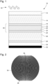
- FIG. 1 illustrates a reflective liquid crystal display device 10 of a watch according to one embodiment of the invention.
- the display device 10 includes an absorbent and transmissive front polarizer 12 (absorbent for light polarization and transmissive for orthogonal polarization), a transparent front substrate 14, a structured transparent front electrode 16, a front alignment layer 18 , a liquid crystal composition 20, a rear alignment layer 22, a structured transparent rear electrode 24, a rear substrate 26, a decorative pattern 28, a reflective and transmissive rear polarizer 30 and a black background 32 (or, according to one another embodiment, colored).
- the rear polarizer 30 can be an absorbing and transmissive polarizer associated with a reflector.
- the display device 10 is reflective in the sense that the incident surrounding light 34 is used as a light source for the display.
- the incident surrounding light 34 passes through the different layers of the display device 10 in the order listed above, is reflected on the rear polarizer 30 and returns towards the user's eye.
- the superposition of the structured electrodes 16, 24 defines a set of shape pixels that can be switched between two optical states.
- the electrodes 16, 24 are connected to a voltage source (not shown) via a control circuit (not shown).
- the application of voltage (or the absence of application) makes it possible to carry out a switching between the two optical states of the liquid crystals 20.
- the front substrate 14 and the rear substrate 26 may be made of glass or plastic.
- the substrates 14, 26 are arranged in opposite directions to create a liquid crystal cell 36 between the front substrate and the rear substrate.
- the liquid crystal cell 36 which includes the front electrode 16, the front alignment layer 18, the liquid crystal composition 20, the rear alignment layer 22 and the rear electrode 24.
- the alignment layers 18, 22 force the liquid crystals 20 to adopt a helical configuration when no electric field is applied by the electrodes 16, 24.
- the alignment layers 18, 22 can be, e.g. e.g., polyimide.
- the display device 10 can operate in “normally white” mode, that is to say a mode in which light is reflected when no electric field is applied to the liquid crystals, or in “normally black” mode, that is to say a mode in which light is not reflected when no electric field is not applied to liquid crystals.
- “normally white” mode that is to say a mode in which light is reflected when no electric field is applied to the liquid crystals
- “normally black” mode that is to say a mode in which light is not reflected when no electric field is not applied to liquid crystals.
- the other optical state is reached when an electric field is applied between the electrodes 16, 24.
- the liquid crystals 20 of the display device 10 are arranged according to several units (also called shape pixels), defined by the structured electrodes 16, 24, switchable independently in the sense that the optical state of a first pixel of shape n does not affect the optical state of a second shape pixel directly adjacent to the first shape pixel.
- the different shape pixels are switched using a voltage delivered by the structured electrodes 16, 24.
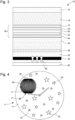
- Fig. 2 illustrates a possible structuring of the electrodes 16, 24.
- Pixels of shape 38 i in black on the Fig. 2
- in the shape of crescents are defined in order to be able to selectively switch the state of the liquid crystals located at the pixels of shape 38 i , between the front electrode 16 and the rear electrode 24.
- a pixel of switching shape 38 i covers one or more elements of the decorative layer. These elements may be continuous parts of the decorative pattern and/or pixels forming said decorative pattern in the case of a high resolution image.
- Shape pixels can be arranged regularly (e.g. for raster displays) or not. The shape of shape pixels is not limited. As indicated above, they can have, for example, a crescent shape, or more simply a rectangular or square shape when observed from above the display.
- the front substrate 14 and/or the rear substrate 26 have a thickness in the range from 50 ⁇ m to 1 mm, preferably in the range from 80 ⁇ m to 0.5 mm.
- the decorative pattern 28 is digitally printed by inkjet directly on the external surface of the rear substrate 26.
- the pattern may include absorbent zones and transparent zones allowing the light to (partially) pass through. through the decorative pattern to reach the rear polarizer 30.
- the fact of directly printing the decorative layer on the substrate 26 mitigates several disadvantages of the solutions proposed by the prior art.
- the alignment between the elements of the decorative pattern and the switching segments 38 i is more precise.
- the alignment can generally be achieved with a precision of 5 ⁇ m or less, because the decorative pattern 28 is very close to the switching segments 38 i defined by the structured electrodes 16,24 compared to the solutions of the prior art.
- This has the consequence that the switching segments 38 i cover exactly the desired areas of the decorative pattern, regardless of the viewing angle of the display device.
- the offset is less than 5 ⁇ m and will therefore not be visible to the naked eye by the user. The aesthetics will appear flawless.
- the alignment can be carried out optically with respect to the switching segments 38 i during the manufacture of the display, before other layers prevent visualization of the electrodes, in particular the structure of the electrodes.
- the parallax is reduced to the thickness of the substrate alone. The use of thin substrates (50 to 300 ⁇ m) makes it possible to reduce parallax so that the resulting optical defects are not perceptible at the naked eye.
- the decorative pattern 28 includes very small transparent openings, more light can be reflected because the decorative pattern 28 is located directly under the substrate and without a support film between the decorative layer and the rear polarizer 30. light reflected with a large angle of incidence are then less likely to be absorbed. The reflectivity (and therefore the visibility) of the decorative pattern 28 is thus improved compared to the prior art.
- the decorative pattern 28 can be applied to the external surface of the front substrate 14 instead of being applied to the external surface of the rear substrate 26 (see first embodiment). It is obviously possible to combine the first and second embodiments in order to obtain a display device comprising two decorative patterns.
- one or more photo-structurable resins can be deposited and structured by photolithography on the external surface of the front substrate 14 and/or on the external surface of the rear substrate 26.
- the resins can be colored or black and be arranged so as to form a decorative pattern 28 after deposition.
- the decorative pattern 28 can be a thin metallic layer (e.g. a layer of aluminum, a layer of gold, a layer of silver, a layer of chrome) and /or dielectric (e.g. a layer of colored oxy-nitrides) deposited by physical or chemical vapor deposition.
- the decorative pattern 28 can be structured, in particular by photolithography-engraving. It is also possible to carry out the deposition and structuring in a single step by deposition through a mask.
- the front substrate may be associated with an absorbing and transmissive front polarizer and the rear substrate may be associated with a reflector.
- the decorative pattern is disposed between the front substrate and the front polarizer.
- the liquid crystal composition may include a dichroic dye.
- the rear substrate is associated with a reflector.
- the decorative pattern can then be placed either on the external surface of the front substrate or between the rear substrate and the reflector.
- the front substrate is associated with a transmissive absorbing polarizer and the rear substrate is associated with a reflector.
- the decorative pattern can then be placed either between the front polarizer and the front substrate or between the rear substrate and the reflector.
- the rear substrate is associated with an absorbing reflective rear polarizer. The decorative pattern can then be placed between the rear polarizer and the rear substrate.
- the display device 10 can be transflective.
- the display device 10 comprises a backlight 40 arranged at the rear of a semi-transparent black background 32 (see Fig. 3 ).
- the semi-transparent black background 32 could be replaced by an absorbing/transparent polarizer.
- the rear polarizer 30 could be replaced by a reflective/transmissive polarizer partially effective in its reflective function, and the black background 32 would be replaced by an absorbing/transmissive polarizer or a semi-reflective background. -absorbent.
- the rear polarizer assembly 30 and the black background 32 would be replaced by a transflective polarizer.
- the backlight emits light 42 and may include one or more inorganic light-emitting diodes and/or one or more organic light-emitting diodes.
- the display device 10 can be transmissive.
- the display device 10 comprises a backlighting 40 arranged at the rear of a display device characterized in that the rear polarizer 30 is an absorbing/transmissive polarizer and that there is no longer a black background.
- An example of application of such a display device in watchmaking or jewelry consists of producing a moon phase by combining a high-resolution decorative pattern of the moon with a liquid crystal cell whose electrode segments are arranged to form a multitude of crescents (see Fig. 2 ) which, aligned with the decorative pattern of the moon, make it possible to display the evolution of the phases of the moon.
- the liquid crystal display device serves to hide the parts of the moon that are currently hidden by the Earth's shadow.
- the electrodes include other segments to display additional information such as time, date, day, meteorological, barometric, altimetric information or to animate decorative or playful elements such as twinkling stars in the starry sky around the Moon.
- the present invention also has an interest in sportswear type products.
- the pattern being an image of a star and the display device comprising a plurality of pixels of switchable shape defined by the transparent structured electrodes representing shaped segments capable of representing an animated image of said star in order to represent said eclipse.
- the transparent structured electrodes representing shaped segments capable of representing an animated image of said star in order to represent said eclipse.
- other celestial objects such as comets, natural satellites or not can be represented in a similar manner on the dynamic display.
- the associated backlighting device can emit a modular color to better match the reality of the colors of the object of the pattern to be represented, particularly during partial or total eclipses.
- a dial assembly 44 for a timepiece comprising a dial 46 and a display device liquid crystals 48 of the type described in connection with the figures 1 to 3 .
- the display device 48 is visible through a window 50 provided in the dial 46.
- the dial 46 includes a fixed image which forms the sky with fixed stars 52, and the decorative pattern of the display represents a moon in the form of several pixels of shape 38i as described previously in connection with the figure 2 , said pattern being able to represent the evolution of the phases of the moon in a dynamic manner.
- the decorative pattern may represent, in the form of a set of shaped pixels, certain planets, comets or other celestial objects (natural satellites or not) which will be represented by the liquid crystal display device in a dynamic manner.
Landscapes
- Physics & Mathematics (AREA)
- Nonlinear Science (AREA)
- General Physics & Mathematics (AREA)
- Optics & Photonics (AREA)
- Crystallography & Structural Chemistry (AREA)
- Chemical & Material Sciences (AREA)
- Mathematical Physics (AREA)
- Geometry (AREA)
- Liquid Crystal (AREA)
- Astronomy & Astrophysics (AREA)
- Electric Clocks (AREA)
- Devices For Indicating Variable Information By Combining Individual Elements (AREA)
- Polarising Elements (AREA)
Claims (19)
- Flüssigkristall-Anzeigevorrichtung, wobei die Anzeigevorrichtung Folgendes umfasst:zwei gegenüberliegende transparente Substrate, die als vorderes Substrat bzw. hinteres Substrat bezeichnet werden, wobei das vordere Substrat das auf der Betrachterseite angeordnete ist und das vordere und das hintere Substrat auf ihren Innenflächen mit transparenten strukturierten Elektroden versehen sind, deren Überlagerung Formpixel definiert, die zwischen zwei optischen Zuständen umschaltbar sind, wobei die Elektroden über eine Steuerschaltung mit einer Spannungsquelle verbunden sind und eine durch einen Dichtungsrahmen geschlossene Zelle bilden, um in dem Bereich, der durch die Substrate und den Dichtungsrahmen begrenzt wird, eine Flüssigkristallzusammensetzung aufzunehmen; undein dekoratives Muster, das in direktem Kontakt mit dem vorderen Substrat und/oder dem hinteren Substrat steht und dadurch gekennzeichnet ist, dass das dekorative Muster mit den strukturierten Elektroden ausgerichtete Elemente aufweist, so dass die Formpixel ein oder mehrere Elemente des dekorativen Musters bedecken, und dadurch, dass das dekorative Muster entweder durch Digitaldruck mittels Tintenstrahl- oder Laserdruck, oder durch Aufbringen und Strukturieren eines lichtempfindlichen Harzes, oder durch physikalisches oder chemisches Dampfabscheiden einer dünnen Metall- und/oder dielektrischen Schicht und Strukturieren der abgeschiedenen dünnen Schicht, oder durch eine Kombination dieser Verfahren aufgebracht wird.
- Anzeigevorrichtung nach Anspruch 1, dadurch gekennzeichnet, dass das dekorative Muster auf einer Außenfläche des vorderen oder des hinteren Substrats angeordnet ist.
- Anzeigevorrichtung nach Anspruch 1 oder 2, dadurch gekennzeichnet, dass das dekorative Muster auf der Außenfläche des hinteren Substrats angeordnet ist.
- Anzeigevorrichtung nach einem der vorhergehenden Ansprüche, dadurch gekennzeichnet, dass das dekorative Muster die Kombination aus einer lichtempfindlichen oder nicht lichtempfindlichen strukturierten Tintenschicht und einer dünnen Metallschicht umfasst, wobei die Anordnung dieser dekorativen Schichten direkt vom vorderen Substrat oder vom hinteren Substrat getragen wird.
- Anzeigevorrichtung nach einem der Ansprüche 1 bis 4, wobei das vordere Substrat mit einem durchlässigen und absorbierenden vorderen Polarisator verbunden ist und wobei das hintere Substrat mit einem absorbierenden und reflektierenden hinteren Polarisator verbunden ist, und wobei das dekorative Muster zwischen dem hinteren Substrat und dem hinteren Polarisator angeordnet ist.
- Anzeigevorrichtung nach einem der Ansprüche 1 bis 4, wobei das vordere Substrat mit einem durchlässigen und absorbierenden vorderen Polarisator verbunden ist und wobei das hintere Substrat mit einem absorbierenden und reflektierenden hinteren Polarisator verbunden ist, und wobei das dekorative Muster zwischen dem vorderen Substrat und dem vorderen Polarisator angeordnet ist.
- Anzeigevorrichtung nach einem der Ansprüche 1 bis 4, wobei das vordere Substrat mit einem durchlässigen und absorbierenden vorderen Polarisator verbunden ist und wobei das hintere Substrat mit einem Reflektor verbunden ist und wobei das dekorative Muster zwischen dem vorderen Substrat und dem vorderen Polarisator angeordnet ist.
- Anzeigevorrichtung nach einem der Ansprüche 1 bis 4, wobei die Flüssigkristallzusammensetzung einen dichroitischen Farbstoff umfasst und wobei das hintere Substrat mit einem Reflektor verbunden ist und wobei das dekorative Muster entweder auf der Außenfläche des vorderen Substrats oder zwischen dem hinteren Substrat und dem Reflektor angeordnet ist.
- Anzeigevorrichtung nach einem der Ansprüche 1 bis 4, wobei die Flüssigkristallzusammensetzung einen dichroitischen Farbstoff umfasst, wobei das vordere Substrat mit einem durchlässigen absorbierenden Polarisator verbunden ist und wobei das hintere Substrat mit einem Reflektor verbunden ist und wobei das dekorative Muster entweder zwischen dem vorderen Polarisator und dem vorderen Substrat oder zwischen dem hinteren Substrat und dem Reflektor angeordnet ist.
- Anzeigevorrichtung nach einem der Ansprüche 1 bis 4, wobei die Flüssigkristallzusammensetzung einen dichroitischen Farbstoff umfasst, wobei das hintere Substrat mit einem absorbierenden reflektierenden hinteren Polarisator verbunden ist und wobei das dekorative Muster zwischen dem hinteren Polarisator und dem hinteren Substrat angeordnet ist.
- Anzeigevorrichtung nach einem der Ansprüche 5, 6 oder 10, wobei der hintere Polarisator durch einen transflektiven Polarisator ersetzt ist und wobei eine Hintergrundbeleuchtungsvorrichtung an der Rückseite des transflektiven Polarisators angeordnet ist.
- Anzeigevorrichtung nach einem der Ansprüche 5, 6 oder 10, wobei der hintere Polarisator durch einen transmissiven absorbierenden Polarisator ersetzt ist und wobei eine Hintergrundbeleuchtungsvorrichtung an der Rückseite des transflektiven Polarisators angeordnet ist.
- Anzeigevorrichtung nach Anspruch 11 oder 12, wobei die Hintergrundbeleuchtungsvorrichtung ein Licht aussendet, dessen Farbe anpassbar ist.
- Anzeigevorrichtung nach einem der Ansprüche, wobei das dekorative Muster in direktem Kontakt mit dem vorderen Substrat und mit dem hinteren Substrat steht und wobei das dekorative Muster aus mindestens zwei zueinander komplementären Musterabschnitten hergestellt wird, wobei die Aneinanderreihung der beiden komplementären Musterabschnitte das dekorative Muster bildet.
- Zifferblattanordnung für eine Uhr, umfassend ein Zifferblatt und eine Anzeigevorrichtung nach einem der Ansprüche 1 bis 14, wobei das Zifferblatt ein statisches Bild trägt, das komplementär zu dem des dekorativen Musters der Anzeigevorrichtung ist.
- Uhr und/oder Schmuckstück, umfassend eine Anzeigevorrichtung nach einem der Ansprüche 1 bis 14.
- Uhr und/oder Schmuckstück nach Anspruch 16, dadurch gekennzeichnet, dass das Muster ein Bild eines Himmelskörpers ist, wobei die Anzeigevorrichtung eine Vielzahl von umschaltbaren Formpixeln umfasst, die durch die transparenten strukturierten Elektroden definiert werden und Formsegmente darstellen, die dazu ausgebildet sind, ein animiertes Bild des Himmelskörpers darzustellen.
- Uhr und/oder Schmuckstück nach Anspruch 17, dadurch gekennzeichnet, dass der Himmelskörper der Mond ist und die Vielzahl von umschaltbaren Formpixeln durch die transparenten strukturierten Elektroden definiert sind und halbmondförmige Segmente darstellen, die die Mondphasen darstellen.
- Verfahren zum Herstellen einer Flüssigkristallanzeigevorrichtung nach einem der Ansprüche 1 bis 18, wobei das Verfahren Folgendes umfasst:Bereitstellen eines vorderen Substrats und eines hinteren Substrats, wobei das vordere und das hintere Substrat auf ihren Innenflächen mit transparenten strukturierten Elektroden versehen sind, deren Überlagerung Formpixel definiert, die zwischen zwei optischen Zuständen umschaltbar sind;Anordnen eines Dichtungsrahmens auf der Innenfläche eines der beiden Substrate;Versiegeln der beiden Substrate miteinander, um einen durch die Substrate begrenzten Bereich zu definieren;Füllen des durch die Substrate begrenzten Bereichs mit einer Flüssigkristallzusammensetzung; undAufbringen eines dekorativen Musters, das in direktem Kontakt mit dem vorderen Substrat oder dem hinteren Substrat steht, und wobei das Aufbringen des dekorativen Musters Folgendes umfasst:∘ entweder durch Digitaldruck des dekorativen Musters mittels Tintenstrahl- oder Laserdruck,∘ oder durch Aufbringen und Strukturieren, vorzugsweise durch Fotolithografie, eines lichtempfindlichen Harzes,∘ oder durch physikalisches oder chemisches Dampfabscheiden einer dünnen Metall- und/oder dielektrischen Schicht und Strukturieren der abgeschiedenen dünnen Schicht, vorzugsweise durch Fotolithografie,∘ oder durch eine Kombination dieser Aufbringungsverfahren.
Priority Applications (6)
| Application Number | Priority Date | Filing Date | Title |
|---|---|---|---|
| EP19217221.1A EP3839617B1 (de) | 2019-12-17 | 2019-12-17 | Flüssigkristall-anzeigevorrichtung |
| US17/000,600 US12007633B2 (en) | 2019-12-17 | 2020-08-24 | Liquid crystal display device with decorative pattern directly thereon |
| JP2020151791A JP2021096222A (ja) | 2019-12-17 | 2020-09-10 | 液晶ディスプレイ・デバイス |
| CN202011491337.9A CN112987365A (zh) | 2019-12-17 | 2020-12-17 | 液晶显示装置 |
| JP2022152746A JP7334318B2 (ja) | 2019-12-17 | 2022-09-26 | 液晶ディスプレイ・デバイス |
| US18/480,718 US12140829B2 (en) | 2019-12-17 | 2023-10-04 | Liquid crystal display device with decorative pattern directly aligned with transparent structured electrodes |
Applications Claiming Priority (1)
| Application Number | Priority Date | Filing Date | Title |
|---|---|---|---|
| EP19217221.1A EP3839617B1 (de) | 2019-12-17 | 2019-12-17 | Flüssigkristall-anzeigevorrichtung |
Publications (2)
| Publication Number | Publication Date |
|---|---|
| EP3839617A1 EP3839617A1 (de) | 2021-06-23 |
| EP3839617B1 true EP3839617B1 (de) | 2024-06-26 |
Family
ID=68944356
Family Applications (1)
| Application Number | Title | Priority Date | Filing Date |
|---|---|---|---|
| EP19217221.1A Active EP3839617B1 (de) | 2019-12-17 | 2019-12-17 | Flüssigkristall-anzeigevorrichtung |
Country Status (4)
| Country | Link |
|---|---|
| US (2) | US12007633B2 (de) |
| EP (1) | EP3839617B1 (de) |
| JP (2) | JP2021096222A (de) |
| CN (1) | CN112987365A (de) |
Families Citing this family (3)
| Publication number | Priority date | Publication date | Assignee | Title |
|---|---|---|---|---|
| JP2022129506A (ja) * | 2021-02-25 | 2022-09-06 | 日東電工株式会社 | 加飾フィルム |
| CN119148432A (zh) * | 2023-06-15 | 2024-12-17 | 群创光电股份有限公司 | 电子装置 |
| CN118033942A (zh) * | 2024-02-22 | 2024-05-14 | 惠科股份有限公司 | 一种显示面板、显示装置和显示系统 |
Citations (4)
| Publication number | Priority date | Publication date | Assignee | Title |
|---|---|---|---|---|
| US20020071069A1 (en) * | 1997-08-01 | 2002-06-13 | Koji Nakagawa | Light scattering type liquid crystal display panel for timepiece |
| US20040257496A1 (en) * | 2003-06-20 | 2004-12-23 | Casio Computer Co., Ltd. | Display device and manufacturing method of the same |
| JP2008083607A (ja) * | 2006-09-29 | 2008-04-10 | Casio Comput Co Ltd | 液晶表示装置およびその製造方法 |
| US20080123473A1 (en) * | 2005-08-10 | 2008-05-29 | Seiko Epson Corporation | Electronic component and electronic device |
Family Cites Families (20)
| Publication number | Priority date | Publication date | Assignee | Title |
|---|---|---|---|---|
| JPS5560921A (en) | 1978-11-01 | 1980-05-08 | Toshiba Corp | Liquid crystal display element |
| US5245590A (en) * | 1992-07-10 | 1993-09-14 | Galison William A | Display of changing moon on watch face |
| FR2743924B1 (fr) * | 1996-01-23 | 1998-05-22 | Asulab Sa | Dispositif d'affichage d'un decor et piece d'horlogerie le comprenant |
| JP3702643B2 (ja) | 1997-06-09 | 2005-10-05 | セイコーエプソン株式会社 | 表示装置及び電子時計 |
| EP0939331B1 (de) * | 1998-02-27 | 2010-04-14 | Asulab S.A. | Anzeigeeinheit mit zwei aufeinander liegenden Anzeigevorrichtungen |
| JP2000221282A (ja) * | 1999-01-29 | 2000-08-11 | Citizen Watch Co Ltd | 時 計 |
| US20050030836A1 (en) * | 2003-04-04 | 2005-02-10 | Tom Burns | Watch with mirror dial plate |
| JP2004329692A (ja) * | 2003-05-09 | 2004-11-25 | Hitachi Displays Ltd | 表示装置および遊技機 |
| JP2007047030A (ja) | 2005-08-10 | 2007-02-22 | Seiko Epson Corp | 計時装置及び計時装置用文字板 |
| US20070153162A1 (en) * | 2005-12-30 | 2007-07-05 | Wright Robin E | Reinforced reflective polarizer films |
| US20090102824A1 (en) * | 2006-03-15 | 2009-04-23 | Sharp Kabushiki Kaisha | Active matrix substrate and display device using the same |
| JP2009008710A (ja) | 2007-06-26 | 2009-01-15 | Citizen Holdings Co Ltd | 液晶表示装置 |
| JP4900206B2 (ja) * | 2007-11-26 | 2012-03-21 | パナソニック株式会社 | タッチパネル |
| US8760415B2 (en) * | 2009-03-30 | 2014-06-24 | Kent Displays Incorporated | Display with overlayed electronic skin |
| CN202230680U (zh) | 2011-09-20 | 2012-05-23 | 吴重九 | 叠合式投影显示装置 |
| US9320140B2 (en) * | 2011-12-22 | 2016-04-19 | Nissha Printing Co., Ltd. | Touch sensor with ornament, method of manufacturing same, and transparent conductive sensor used in same |
| US20140098332A1 (en) * | 2012-10-10 | 2014-04-10 | Apple Inc. | Displays With Logos and Alignment Marks |
| US9297675B2 (en) * | 2013-10-04 | 2016-03-29 | Tactotek Oy | Illuminated indicator structures for electronic devices |
| DE112015004066T5 (de) * | 2014-09-05 | 2017-05-11 | Denso Corporation | Anzeigevorrichtung |
| US20180267345A1 (en) * | 2017-03-15 | 2018-09-20 | HKC Corporation Limited | Display device and display panel thereof |
-
2019
- 2019-12-17 EP EP19217221.1A patent/EP3839617B1/de active Active
-
2020
- 2020-08-24 US US17/000,600 patent/US12007633B2/en active Active
- 2020-09-10 JP JP2020151791A patent/JP2021096222A/ja active Pending
- 2020-12-17 CN CN202011491337.9A patent/CN112987365A/zh active Pending
-
2022
- 2022-09-26 JP JP2022152746A patent/JP7334318B2/ja active Active
-
2023
- 2023-10-04 US US18/480,718 patent/US12140829B2/en active Active
Patent Citations (4)
| Publication number | Priority date | Publication date | Assignee | Title |
|---|---|---|---|---|
| US20020071069A1 (en) * | 1997-08-01 | 2002-06-13 | Koji Nakagawa | Light scattering type liquid crystal display panel for timepiece |
| US20040257496A1 (en) * | 2003-06-20 | 2004-12-23 | Casio Computer Co., Ltd. | Display device and manufacturing method of the same |
| US20080123473A1 (en) * | 2005-08-10 | 2008-05-29 | Seiko Epson Corporation | Electronic component and electronic device |
| JP2008083607A (ja) * | 2006-09-29 | 2008-04-10 | Casio Comput Co Ltd | 液晶表示装置およびその製造方法 |
Also Published As
| Publication number | Publication date |
|---|---|
| US12007633B2 (en) | 2024-06-11 |
| US12140829B2 (en) | 2024-11-12 |
| EP3839617A1 (de) | 2021-06-23 |
| JP7334318B2 (ja) | 2023-08-28 |
| US20240027807A1 (en) | 2024-01-25 |
| US20210181564A1 (en) | 2021-06-17 |
| CN112987365A (zh) | 2021-06-18 |
| JP2022188135A (ja) | 2022-12-20 |
| JP2021096222A (ja) | 2021-06-24 |
Similar Documents
| Publication | Publication Date | Title |
|---|---|---|
| EP0786685B1 (de) | Verzierung anzeigende Vorrichtung und diese enthaltende Uhr | |
| EP1128240B1 (de) | Eine zwei übereinander angeordnete Anzeigevorrichtungen umfassende Anzeigeeinheit mit Kontrastinversion | |
| EP1040391B1 (de) | Anzeigeeinheit mit zwei übereinander liegenden anzeigevorrichtungen | |
| US12140829B2 (en) | Liquid crystal display device with decorative pattern directly aligned with transparent structured electrodes | |
| EP0078237B1 (de) | Uhr mit analoger Anzeige, deren Zifferblatt aus einer Flüssigkeitskristallanzeigezelle besteht | |
| EP3069199B1 (de) | Perlmutterziffernblatt für eine verborgene anzeige | |
| EP3650957B1 (de) | Gegenstand, der mit einer elektrooptischen anzeigevorrichtung ausgestattet ist | |
| WO2007096358A1 (fr) | Dispositif d'affichage à cristaux liquides affichant des segments colorés et pièce d'horlogerie équipée de ce dispositif | |
| CH716960A2 (fr) | Dispositif d'affichage à cristaux liquides. | |
| EP1189095A1 (de) | Zweifarbige Flüssigkristallanzeigeeinheit | |
| EP0939331B1 (de) | Anzeigeeinheit mit zwei aufeinander liegenden Anzeigevorrichtungen | |
| HK40055763A (en) | Liquid crystal display device | |
| EP1174756B1 (de) | Anzeigeeinheit mit einer elektrooptischen und einer photovoltaischen Zelle | |
| CH715286B1 (fr) | Objet muni d'un dispositif d`affichage électrooptique. | |
| EP4016173B1 (de) | Verfahren zur herstellung einer flüssigkristallanzeigevorrichtung und flüssigkristallanzeigevorrichtung | |
| EP1085364B1 (de) | Anzeigeeinheit mit zwei übereinander angeordneten Anzeigenvorrichtungen | |
| EP3128359A1 (de) | Anzeigevorrichtung fuer ein tragbares instrument, wie beispielsweise eine uhr | |
| EP1202109A1 (de) | Flüssigkristallanzeigeeinrichtung mit hohem Reflexionskoeffizienten | |
| EP1209512A1 (de) | Reflektierende Flüssigkristallanzeige mit verbessertem Kontrast | |
| EP1156360B1 (de) | Anzeigeeinheit mit chromatischer Kontrastumkehrung | |
| FR3021800A1 (fr) | Dispositif d'affichage reflectif a tres haute luminosite et a surface photovoltaique integree | |
| CH708838A2 (fr) | Cadran translucide ou semi-transparent pour afficheur caché. | |
| CH711421A2 (fr) | Dispositif d'affichage pour un objet portable tel qu'une pièce d'horlogerie comprenant un réseau lenticulaire. |
Legal Events
| Date | Code | Title | Description |
|---|---|---|---|
| PUAI | Public reference made under article 153(3) epc to a published international application that has entered the european phase |
Free format text: ORIGINAL CODE: 0009012 |
|
| STAA | Information on the status of an ep patent application or granted ep patent |
Free format text: STATUS: THE APPLICATION HAS BEEN PUBLISHED |
|
| AK | Designated contracting states |
Kind code of ref document: A1 Designated state(s): AL AT BE BG CH CY CZ DE DK EE ES FI FR GB GR HR HU IE IS IT LI LT LU LV MC MK MT NL NO PL PT RO RS SE SI SK SM TR |
|
| STAA | Information on the status of an ep patent application or granted ep patent |
Free format text: STATUS: REQUEST FOR EXAMINATION WAS MADE |
|
| 17P | Request for examination filed |
Effective date: 20211223 |
|
| RBV | Designated contracting states (corrected) |
Designated state(s): AL AT BE BG CH CY CZ DE DK EE ES FI FR GB GR HR HU IE IS IT LI LT LU LV MC MK MT NL NO PL PT RO RS SE SI SK SM TR |
|
| STAA | Information on the status of an ep patent application or granted ep patent |
Free format text: STATUS: EXAMINATION IS IN PROGRESS |
|
| 17Q | First examination report despatched |
Effective date: 20230209 |
|
| P01 | Opt-out of the competence of the unified patent court (upc) registered |
Effective date: 20230615 |
|
| GRAP | Despatch of communication of intention to grant a patent |
Free format text: ORIGINAL CODE: EPIDOSNIGR1 |
|
| STAA | Information on the status of an ep patent application or granted ep patent |
Free format text: STATUS: GRANT OF PATENT IS INTENDED |
|
| INTG | Intention to grant announced |
Effective date: 20240402 |
|
| GRAS | Grant fee paid |
Free format text: ORIGINAL CODE: EPIDOSNIGR3 |
|
| GRAA | (expected) grant |
Free format text: ORIGINAL CODE: 0009210 |
|
| STAA | Information on the status of an ep patent application or granted ep patent |
Free format text: STATUS: THE PATENT HAS BEEN GRANTED |
|
| AK | Designated contracting states |
Kind code of ref document: B1 Designated state(s): AL AT BE BG CH CY CZ DE DK EE ES FI FR GB GR HR HU IE IS IT LI LT LU LV MC MK MT NL NO PL PT RO RS SE SI SK SM TR |
|
| REG | Reference to a national code |
Ref country code: GB Ref legal event code: FG4D Free format text: NOT ENGLISH |
|
| REG | Reference to a national code |
Ref country code: CH Ref legal event code: EP |
|
| REG | Reference to a national code |
Ref country code: DE Ref legal event code: R096 Ref document number: 602019054129 Country of ref document: DE |
|
| PG25 | Lapsed in a contracting state [announced via postgrant information from national office to epo] |
Ref country code: BG Free format text: LAPSE BECAUSE OF FAILURE TO SUBMIT A TRANSLATION OF THE DESCRIPTION OR TO PAY THE FEE WITHIN THE PRESCRIBED TIME-LIMIT Effective date: 20240626 |
|
| PG25 | Lapsed in a contracting state [announced via postgrant information from national office to epo] |
Ref country code: HR Free format text: LAPSE BECAUSE OF FAILURE TO SUBMIT A TRANSLATION OF THE DESCRIPTION OR TO PAY THE FEE WITHIN THE PRESCRIBED TIME-LIMIT Effective date: 20240626 Ref country code: FI Free format text: LAPSE BECAUSE OF FAILURE TO SUBMIT A TRANSLATION OF THE DESCRIPTION OR TO PAY THE FEE WITHIN THE PRESCRIBED TIME-LIMIT Effective date: 20240626 |
|
| REG | Reference to a national code |
Ref country code: LT Ref legal event code: MG9D |
|
| PG25 | Lapsed in a contracting state [announced via postgrant information from national office to epo] |
Ref country code: GR Free format text: LAPSE BECAUSE OF FAILURE TO SUBMIT A TRANSLATION OF THE DESCRIPTION OR TO PAY THE FEE WITHIN THE PRESCRIBED TIME-LIMIT Effective date: 20240927 |
|
| PG25 | Lapsed in a contracting state [announced via postgrant information from national office to epo] |
Ref country code: LV Free format text: LAPSE BECAUSE OF FAILURE TO SUBMIT A TRANSLATION OF THE DESCRIPTION OR TO PAY THE FEE WITHIN THE PRESCRIBED TIME-LIMIT Effective date: 20240626 |
|
| REG | Reference to a national code |
Ref country code: NL Ref legal event code: MP Effective date: 20240626 |
|
| PG25 | Lapsed in a contracting state [announced via postgrant information from national office to epo] |
Ref country code: NO Free format text: LAPSE BECAUSE OF FAILURE TO SUBMIT A TRANSLATION OF THE DESCRIPTION OR TO PAY THE FEE WITHIN THE PRESCRIBED TIME-LIMIT Effective date: 20240926 Ref country code: LV Free format text: LAPSE BECAUSE OF FAILURE TO SUBMIT A TRANSLATION OF THE DESCRIPTION OR TO PAY THE FEE WITHIN THE PRESCRIBED TIME-LIMIT Effective date: 20240626 Ref country code: HR Free format text: LAPSE BECAUSE OF FAILURE TO SUBMIT A TRANSLATION OF THE DESCRIPTION OR TO PAY THE FEE WITHIN THE PRESCRIBED TIME-LIMIT Effective date: 20240626 Ref country code: GR Free format text: LAPSE BECAUSE OF FAILURE TO SUBMIT A TRANSLATION OF THE DESCRIPTION OR TO PAY THE FEE WITHIN THE PRESCRIBED TIME-LIMIT Effective date: 20240927 Ref country code: FI Free format text: LAPSE BECAUSE OF FAILURE TO SUBMIT A TRANSLATION OF THE DESCRIPTION OR TO PAY THE FEE WITHIN THE PRESCRIBED TIME-LIMIT Effective date: 20240626 Ref country code: BG Free format text: LAPSE BECAUSE OF FAILURE TO SUBMIT A TRANSLATION OF THE DESCRIPTION OR TO PAY THE FEE WITHIN THE PRESCRIBED TIME-LIMIT Effective date: 20240626 Ref country code: RS Free format text: LAPSE BECAUSE OF FAILURE TO SUBMIT A TRANSLATION OF THE DESCRIPTION OR TO PAY THE FEE WITHIN THE PRESCRIBED TIME-LIMIT Effective date: 20240926 |
|
| PG25 | Lapsed in a contracting state [announced via postgrant information from national office to epo] |
Ref country code: NL Free format text: LAPSE BECAUSE OF FAILURE TO SUBMIT A TRANSLATION OF THE DESCRIPTION OR TO PAY THE FEE WITHIN THE PRESCRIBED TIME-LIMIT Effective date: 20240626 |
|
| REG | Reference to a national code |
Ref country code: AT Ref legal event code: MK05 Ref document number: 1698190 Country of ref document: AT Kind code of ref document: T Effective date: 20240626 |
|
| PG25 | Lapsed in a contracting state [announced via postgrant information from national office to epo] |
Ref country code: NL Free format text: LAPSE BECAUSE OF FAILURE TO SUBMIT A TRANSLATION OF THE DESCRIPTION OR TO PAY THE FEE WITHIN THE PRESCRIBED TIME-LIMIT Effective date: 20240626 |
|
| PG25 | Lapsed in a contracting state [announced via postgrant information from national office to epo] |
Ref country code: PT Free format text: LAPSE BECAUSE OF FAILURE TO SUBMIT A TRANSLATION OF THE DESCRIPTION OR TO PAY THE FEE WITHIN THE PRESCRIBED TIME-LIMIT Effective date: 20241028 |
|
| PG25 | Lapsed in a contracting state [announced via postgrant information from national office to epo] |
Ref country code: PT Free format text: LAPSE BECAUSE OF FAILURE TO SUBMIT A TRANSLATION OF THE DESCRIPTION OR TO PAY THE FEE WITHIN THE PRESCRIBED TIME-LIMIT Effective date: 20241028 |
|
| PGFP | Annual fee paid to national office [announced via postgrant information from national office to epo] |
Ref country code: DE Payment date: 20241121 Year of fee payment: 6 |
|
| PG25 | Lapsed in a contracting state [announced via postgrant information from national office to epo] |
Ref country code: PL Free format text: LAPSE BECAUSE OF FAILURE TO SUBMIT A TRANSLATION OF THE DESCRIPTION OR TO PAY THE FEE WITHIN THE PRESCRIBED TIME-LIMIT Effective date: 20240626 |
|
| PGFP | Annual fee paid to national office [announced via postgrant information from national office to epo] |
Ref country code: FR Payment date: 20241121 Year of fee payment: 6 |
|
| PG25 | Lapsed in a contracting state [announced via postgrant information from national office to epo] |
Ref country code: EE Free format text: LAPSE BECAUSE OF FAILURE TO SUBMIT A TRANSLATION OF THE DESCRIPTION OR TO PAY THE FEE WITHIN THE PRESCRIBED TIME-LIMIT Effective date: 20240626 |
|
| PG25 | Lapsed in a contracting state [announced via postgrant information from national office to epo] |
Ref country code: IS Free format text: LAPSE BECAUSE OF FAILURE TO SUBMIT A TRANSLATION OF THE DESCRIPTION OR TO PAY THE FEE WITHIN THE PRESCRIBED TIME-LIMIT Effective date: 20241026 Ref country code: AT Free format text: LAPSE BECAUSE OF FAILURE TO SUBMIT A TRANSLATION OF THE DESCRIPTION OR TO PAY THE FEE WITHIN THE PRESCRIBED TIME-LIMIT Effective date: 20240626 |
|
| PG25 | Lapsed in a contracting state [announced via postgrant information from national office to epo] |
Ref country code: CZ Free format text: LAPSE BECAUSE OF FAILURE TO SUBMIT A TRANSLATION OF THE DESCRIPTION OR TO PAY THE FEE WITHIN THE PRESCRIBED TIME-LIMIT Effective date: 20240626 |
|
| PG25 | Lapsed in a contracting state [announced via postgrant information from national office to epo] |
Ref country code: SK Free format text: LAPSE BECAUSE OF FAILURE TO SUBMIT A TRANSLATION OF THE DESCRIPTION OR TO PAY THE FEE WITHIN THE PRESCRIBED TIME-LIMIT Effective date: 20240626 Ref country code: RO Free format text: LAPSE BECAUSE OF FAILURE TO SUBMIT A TRANSLATION OF THE DESCRIPTION OR TO PAY THE FEE WITHIN THE PRESCRIBED TIME-LIMIT Effective date: 20240626 |
|
| PG25 | Lapsed in a contracting state [announced via postgrant information from national office to epo] |
Ref country code: ES Free format text: LAPSE BECAUSE OF FAILURE TO SUBMIT A TRANSLATION OF THE DESCRIPTION OR TO PAY THE FEE WITHIN THE PRESCRIBED TIME-LIMIT Effective date: 20240626 Ref country code: SM Free format text: LAPSE BECAUSE OF FAILURE TO SUBMIT A TRANSLATION OF THE DESCRIPTION OR TO PAY THE FEE WITHIN THE PRESCRIBED TIME-LIMIT Effective date: 20240626 |
|
| PG25 | Lapsed in a contracting state [announced via postgrant information from national office to epo] |
Ref country code: SM Free format text: LAPSE BECAUSE OF FAILURE TO SUBMIT A TRANSLATION OF THE DESCRIPTION OR TO PAY THE FEE WITHIN THE PRESCRIBED TIME-LIMIT Effective date: 20240626 Ref country code: SK Free format text: LAPSE BECAUSE OF FAILURE TO SUBMIT A TRANSLATION OF THE DESCRIPTION OR TO PAY THE FEE WITHIN THE PRESCRIBED TIME-LIMIT Effective date: 20240626 Ref country code: RO Free format text: LAPSE BECAUSE OF FAILURE TO SUBMIT A TRANSLATION OF THE DESCRIPTION OR TO PAY THE FEE WITHIN THE PRESCRIBED TIME-LIMIT Effective date: 20240626 Ref country code: PL Free format text: LAPSE BECAUSE OF FAILURE TO SUBMIT A TRANSLATION OF THE DESCRIPTION OR TO PAY THE FEE WITHIN THE PRESCRIBED TIME-LIMIT Effective date: 20240626 Ref country code: IS Free format text: LAPSE BECAUSE OF FAILURE TO SUBMIT A TRANSLATION OF THE DESCRIPTION OR TO PAY THE FEE WITHIN THE PRESCRIBED TIME-LIMIT Effective date: 20241026 Ref country code: ES Free format text: LAPSE BECAUSE OF FAILURE TO SUBMIT A TRANSLATION OF THE DESCRIPTION OR TO PAY THE FEE WITHIN THE PRESCRIBED TIME-LIMIT Effective date: 20240626 Ref country code: EE Free format text: LAPSE BECAUSE OF FAILURE TO SUBMIT A TRANSLATION OF THE DESCRIPTION OR TO PAY THE FEE WITHIN THE PRESCRIBED TIME-LIMIT Effective date: 20240626 Ref country code: CZ Free format text: LAPSE BECAUSE OF FAILURE TO SUBMIT A TRANSLATION OF THE DESCRIPTION OR TO PAY THE FEE WITHIN THE PRESCRIBED TIME-LIMIT Effective date: 20240626 Ref country code: AT Free format text: LAPSE BECAUSE OF FAILURE TO SUBMIT A TRANSLATION OF THE DESCRIPTION OR TO PAY THE FEE WITHIN THE PRESCRIBED TIME-LIMIT Effective date: 20240626 |
|
| PG25 | Lapsed in a contracting state [announced via postgrant information from national office to epo] |
Ref country code: IT Free format text: LAPSE BECAUSE OF FAILURE TO SUBMIT A TRANSLATION OF THE DESCRIPTION OR TO PAY THE FEE WITHIN THE PRESCRIBED TIME-LIMIT Effective date: 20240626 |
|
| REG | Reference to a national code |
Ref country code: DE Ref legal event code: R097 Ref document number: 602019054129 Country of ref document: DE |
|
| PG25 | Lapsed in a contracting state [announced via postgrant information from national office to epo] |
Ref country code: DK Free format text: LAPSE BECAUSE OF FAILURE TO SUBMIT A TRANSLATION OF THE DESCRIPTION OR TO PAY THE FEE WITHIN THE PRESCRIBED TIME-LIMIT Effective date: 20240626 |
|
| PGFP | Annual fee paid to national office [announced via postgrant information from national office to epo] |
Ref country code: CH Payment date: 20250101 Year of fee payment: 6 |
|
| PLBE | No opposition filed within time limit |
Free format text: ORIGINAL CODE: 0009261 |
|
| STAA | Information on the status of an ep patent application or granted ep patent |
Free format text: STATUS: NO OPPOSITION FILED WITHIN TIME LIMIT |
|
| 26N | No opposition filed |
Effective date: 20250327 |
|
| PG25 | Lapsed in a contracting state [announced via postgrant information from national office to epo] |
Ref country code: MC Free format text: LAPSE BECAUSE OF FAILURE TO SUBMIT A TRANSLATION OF THE DESCRIPTION OR TO PAY THE FEE WITHIN THE PRESCRIBED TIME-LIMIT Effective date: 20240626 |
|
| PG25 | Lapsed in a contracting state [announced via postgrant information from national office to epo] |
Ref country code: LU Free format text: LAPSE BECAUSE OF NON-PAYMENT OF DUE FEES Effective date: 20241217 |
|
| GBPC | Gb: european patent ceased through non-payment of renewal fee |
Effective date: 20241217 |
|
| PG25 | Lapsed in a contracting state [announced via postgrant information from national office to epo] |
Ref country code: SE Free format text: LAPSE BECAUSE OF FAILURE TO SUBMIT A TRANSLATION OF THE DESCRIPTION OR TO PAY THE FEE WITHIN THE PRESCRIBED TIME-LIMIT Effective date: 20240626 |
|
| REG | Reference to a national code |
Ref country code: BE Ref legal event code: MM Effective date: 20241231 |
|
| PG25 | Lapsed in a contracting state [announced via postgrant information from national office to epo] |
Ref country code: GB Free format text: LAPSE BECAUSE OF NON-PAYMENT OF DUE FEES Effective date: 20241217 Ref country code: BE Free format text: LAPSE BECAUSE OF NON-PAYMENT OF DUE FEES Effective date: 20241231 |
|
| PG25 | Lapsed in a contracting state [announced via postgrant information from national office to epo] |
Ref country code: IE Free format text: LAPSE BECAUSE OF NON-PAYMENT OF DUE FEES Effective date: 20241217 |