EP3836763A1 - Circuit board having terminal, and circuit board assembly - Google Patents
Circuit board having terminal, and circuit board assembly Download PDFInfo
- Publication number
- EP3836763A1 EP3836763A1 EP19847204.5A EP19847204A EP3836763A1 EP 3836763 A1 EP3836763 A1 EP 3836763A1 EP 19847204 A EP19847204 A EP 19847204A EP 3836763 A1 EP3836763 A1 EP 3836763A1
- Authority
- EP
- European Patent Office
- Prior art keywords
- circuit board
- terminal
- board
- child
- sides
- Prior art date
- Legal status (The legal status is an assumption and is not a legal conclusion. Google has not performed a legal analysis and makes no representation as to the accuracy of the status listed.)
- Pending
Links
Images



Classifications
-
- H—ELECTRICITY
- H01—ELECTRIC ELEMENTS
- H01R—ELECTRICALLY-CONDUCTIVE CONNECTIONS; STRUCTURAL ASSOCIATIONS OF A PLURALITY OF MUTUALLY-INSULATED ELECTRICAL CONNECTING ELEMENTS; COUPLING DEVICES; CURRENT COLLECTORS
- H01R12/00—Structural associations of a plurality of mutually-insulated electrical connecting elements, specially adapted for printed circuits, e.g. printed circuit boards [PCB], flat or ribbon cables, or like generally planar structures, e.g. terminal strips, terminal blocks; Coupling devices specially adapted for printed circuits, flat or ribbon cables, or like generally planar structures; Terminals specially adapted for contact with, or insertion into, printed circuits, flat or ribbon cables, or like generally planar structures
- H01R12/70—Coupling devices
- H01R12/71—Coupling devices for rigid printing circuits or like structures
- H01R12/72—Coupling devices for rigid printing circuits or like structures coupling with the edge of the rigid printed circuits or like structures
- H01R12/722—Coupling devices for rigid printing circuits or like structures coupling with the edge of the rigid printed circuits or like structures coupling devices mounted on the edge of the printed circuits
- H01R12/724—Coupling devices for rigid printing circuits or like structures coupling with the edge of the rigid printed circuits or like structures coupling devices mounted on the edge of the printed circuits containing contact members forming a right angle
-
- H—ELECTRICITY
- H01—ELECTRIC ELEMENTS
- H01Q—ANTENNAS, i.e. RADIO AERIALS
- H01Q1/00—Details of, or arrangements associated with, antennas
- H01Q1/36—Structural form of radiating elements, e.g. cone, spiral, umbrella; Particular materials used therewith
- H01Q1/38—Structural form of radiating elements, e.g. cone, spiral, umbrella; Particular materials used therewith formed by a conductive layer on an insulating support
-
- H—ELECTRICITY
- H01—ELECTRIC ELEMENTS
- H01Q—ANTENNAS, i.e. RADIO AERIALS
- H01Q9/00—Electrically-short antennas having dimensions not more than twice the operating wavelength and consisting of conductive active radiating elements
- H01Q9/04—Resonant antennas
- H01Q9/30—Resonant antennas with feed to end of elongated active element, e.g. unipole
- H01Q9/42—Resonant antennas with feed to end of elongated active element, e.g. unipole with folded element, the folded parts being spaced apart a small fraction of the operating wavelength
-
- H—ELECTRICITY
- H01—ELECTRIC ELEMENTS
- H01R—ELECTRICALLY-CONDUCTIVE CONNECTIONS; STRUCTURAL ASSOCIATIONS OF A PLURALITY OF MUTUALLY-INSULATED ELECTRICAL CONNECTING ELEMENTS; COUPLING DEVICES; CURRENT COLLECTORS
- H01R12/00—Structural associations of a plurality of mutually-insulated electrical connecting elements, specially adapted for printed circuits, e.g. printed circuit boards [PCB], flat or ribbon cables, or like generally planar structures, e.g. terminal strips, terminal blocks; Coupling devices specially adapted for printed circuits, flat or ribbon cables, or like generally planar structures; Terminals specially adapted for contact with, or insertion into, printed circuits, flat or ribbon cables, or like generally planar structures
- H01R12/70—Coupling devices
- H01R12/71—Coupling devices for rigid printing circuits or like structures
- H01R12/712—Coupling devices for rigid printing circuits or like structures co-operating with the surface of the printed circuit or with a coupling device exclusively provided on the surface of the printed circuit
- H01R12/716—Coupling device provided on the PCB
-
- H—ELECTRICITY
- H05—ELECTRIC TECHNIQUES NOT OTHERWISE PROVIDED FOR
- H05K—PRINTED CIRCUITS; CASINGS OR CONSTRUCTIONAL DETAILS OF ELECTRIC APPARATUS; MANUFACTURE OF ASSEMBLAGES OF ELECTRICAL COMPONENTS
- H05K1/00—Printed circuits
- H05K1/02—Details
- H05K1/14—Structural association of two or more printed circuits
- H05K1/141—One or more single auxiliary printed circuits mounted on a main printed circuit, e.g. modules, adapters
-
- H—ELECTRICITY
- H05—ELECTRIC TECHNIQUES NOT OTHERWISE PROVIDED FOR
- H05K—PRINTED CIRCUITS; CASINGS OR CONSTRUCTIONAL DETAILS OF ELECTRIC APPARATUS; MANUFACTURE OF ASSEMBLAGES OF ELECTRICAL COMPONENTS
- H05K3/00—Apparatus or processes for manufacturing printed circuits
- H05K3/36—Assembling printed circuits with other printed circuits
- H05K3/366—Assembling printed circuits with other printed circuits substantially perpendicularly to each other
-
- H—ELECTRICITY
- H05—ELECTRIC TECHNIQUES NOT OTHERWISE PROVIDED FOR
- H05K—PRINTED CIRCUITS; CASINGS OR CONSTRUCTIONAL DETAILS OF ELECTRIC APPARATUS; MANUFACTURE OF ASSEMBLAGES OF ELECTRICAL COMPONENTS
- H05K1/00—Printed circuits
- H05K1/16—Printed circuits incorporating printed electric components, e.g. printed resistors, capacitors or inductors
- H05K1/165—Printed circuits incorporating printed electric components, e.g. printed resistors, capacitors or inductors incorporating printed inductors
-
- H—ELECTRICITY
- H05—ELECTRIC TECHNIQUES NOT OTHERWISE PROVIDED FOR
- H05K—PRINTED CIRCUITS; CASINGS OR CONSTRUCTIONAL DETAILS OF ELECTRIC APPARATUS; MANUFACTURE OF ASSEMBLAGES OF ELECTRICAL COMPONENTS
- H05K2201/00—Indexing scheme relating to printed circuits covered by H05K1/00
- H05K2201/04—Assemblies of printed circuits
- H05K2201/048—Second PCB mounted on first PCB by inserting in window or holes of the first PCB
-
- H—ELECTRICITY
- H05—ELECTRIC TECHNIQUES NOT OTHERWISE PROVIDED FOR
- H05K—PRINTED CIRCUITS; CASINGS OR CONSTRUCTIONAL DETAILS OF ELECTRIC APPARATUS; MANUFACTURE OF ASSEMBLAGES OF ELECTRICAL COMPONENTS
- H05K2201/00—Indexing scheme relating to printed circuits covered by H05K1/00
- H05K2201/10—Details of components or other objects attached to or integrated in a printed circuit board
- H05K2201/10007—Types of components
- H05K2201/10098—Components for radio transmission, e.g. radio frequency identification [RFID] tag, printed or non-printed antennas
Definitions
- the present invention relates to a circuit board having a terminal and to a circuit board assembly into which a plurality of circuit boards are assembled.
- a mounting method In mounting a circuit component on a circuit board, a mounting method has been widely adopted in which a pin-shaped terminal of the circuit board is inserted into a through hole whose inner wall surface is plated with an electrically conductive material and the terminal is soldered within the through hole.
- PTL 1 discloses a coupling structure in which an end of a first circuit board is inserted into a through hole of a second circuit board.
- the coupling structure of PTL 1 since only two surfaces, namely front and back surfaces of the first circuit board, are solderable, there is a risk of insufficient soldering.
- the aforementioned mounting method in which a terminal is inserted into and soldered to a through hole, may be applied to the coupling structure disclosed in PTL 1 listed above. That is, an inner wall surface of the through hole of the second circuit board is plated with an electrically conductive material, the end of the first circuit board is treated as a terminal to be inserted into the through hole, and the end is soldered within the through hole. Adopting this method, which does not require a terminal separately from a circuit board, achieves a reduction in cost.
- the present invention has as an object to provide a circuit board having a terminal, and a circuit board assembly that make it possible to use an end of a circuit board as a terminal and also as a narrow terminal.
- the present invention is directed to a circuit board having a terminal, where the circuit board includes a terminal area that projects from an end face of the circuit board, and the terminal area is flush with a front side and a back side of the circuit board, and is the terminal area is as thick as (has the thickness of) the circuit board.
- the terminal area has four sides covered with an electrically conductive material, and the four sides include a first surface and a second surface that are flush with the front side and the back side of the circuit board, and two side surfaces that intersect the first surface and the second surface.
- the terminal area is covered with an electrically conductive material on both side surfaces as well as the two sides, namely the front and back sides, of the terminal area. For this reason, the terminal area is soldered to a through hole inner surface of a mating board on all sides. This makes it possible to achieve a narrow terminal while satisfying the foregoing standard.
- the circuit board may further include an antenna pattern on at least either of the front and back sides of the circuit board.
- a terminal can be matched in impedance with the antenna pattern.
- the terminal area has a fifth surface at a projecting tip of the terminal area covered with an electrically conductive material.
- the present invention is directed to a circuit board assembly including: a first circuit board serving as the circuit board according to any aspect of the present invention; and a second circuit board having a through hole whose inner wall surface is covered with an electrically conducting material on all sides, wherein the inner wall surface and the four sides are soldered to each other with the terminal area inserted in the though hole.
- the present invention makes it possible to use an end of a circuit board as a narrow terminal that is inserted into and soldered to a through hole.
- Figure 1 is an isometric view of a circuit board assembly according to an embodiment of the present invention.
- This circuit board assembly 100 includes three circuit boards, namely a main board (parent board) 10, a first child board 20, and a second child board 30.
- the first child board 20 has a front surface 21 on which a circuit pattern 22 is formed, and the circuit pattern 22 constitutes a part of an antenna pattern 32 formed mainly on a front surface 31 of the second child board 30.
- This circuit pattern 22 is connected via one of two terminal areas 24 to the antenna pattern 32 formed on the second child board 30.
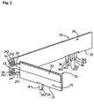
- Figure 2 is an exploded isometric view of a first child board and a second child board that are to be assembled.
- Figure 3 is an isometric view of an assembly of the first child board and the second child board.
- the two terminal areas 24 are provided on a side of the first child board 20 that faces the second child board 30.
- Each of these terminal areas 24 has a shape that projects from a side end face of the first child board 20, that is flush with the front and back sides of the first child board 20, and that is as thick as the first child board 20.
- Each of these terminal areas 24 has a first surface 241 that is flush with the front surface 21 of the first child board 20 and on which an electrically conductive material film is formed and a second surface (not illustrated) that is flush with the back surface of the first child board 20 and on which an electrically conductive material film is formed. Further, both side surfaces of each of the terminal areas 24 that intersect the first surface 241 and the second surface are covered with electrically conductive material films, too. These films on both side surfaces are formed by an electroless plating process which is the same as non-electrolytic plating on an inner wall surface of a through hole. Furthermore, a tip end face 242 of each of the terminal areas 24 that projects from the first child board 20 may be covered with an electrically conductive material film, too. This tip end face 242 is equivalent to an example of the fifth surface of the present invention.
- the second child board 30 is provided with two vertically long through holes 34 into which the two terminal areas 24 of the first child board 20 are inserted, respectively.
- These through holes 34 have their inner wall surfaces covered with electrically conductive material films on all sides thereof by non-electrolytic plating.
- the two terminal areas 24 of the first child board 20 are inserted into the two through holes 34 of the second child board 30, respectively.
- the terminal areas 24 are soldered to the inner wall surfaces of the through holes 34. Since the terminal areas 24 are covered with the electrically conductive material films on all four sides thereof, the terminal areas 24 are soldered on all sides thereof.
- first child board 20 is equivalent to an example of the circuit board having a terminal (first circuit board) of the present invention.
- second child board 30 is equivalent to an example of the second circuit board of the present invention.
- a combination of these first and second child boards 20 and 30 is equivalent to an example of the circuit board assembly of the present invention.
- the first child board 20 includes another terminal area 26 that projects downward from a lower end face 25 of the first child board 20.
- This terminal area 26, too has a projecting shape that is flush with the front and back sides of the first child board 20 and that is as thick as the first child board 20.
- this terminal area 26 has a first surface 261, covered with an electrically conductive material film, that is flush with the front surface 21 of the first child board 20 and a second surface (not illustrated), covered with an electrically conductive material film, that serves as a back surface of the terminal area 26.
- both side surfaces of this terminal area 26 that intersect the first surface 261 and the second surface are covered with electrically conductive material films, too.
- this terminal area 26, too is covered with an electrically conductive material film all around on four sides, namely the first surface 261, the second surface, and both side surfaces.
- a tip end face 262 of the terminal area 26 that projects from the first child board 20 may be covered with an electrically conductive material film, too.
- a solder fillet can be formed into a better shape.
- This tip end face 262 is equivalent to an example of the fifth surface of the present invention.
- the second child board 30 has four terminal areas 36 (see Figure 3 ) that project downward from a lower end face 35 of the second child board 30, and three of them are sequentially arranged in proximity to one another.
- Each of these terminal areas 36 has a projecting shape that is flush with the front and back sides of the second child board 30 and that is as thick as the second child board 30.
- each of these terminal areas 36 has a first surface 361 and a second surface 362, covered with electrically conductive material films, that are flush with the front surface 31 and back surface 39 of the second child board 30, respectively.
- both side surfaces of each of the terminal areas 36 that intersect the first surface 361 and the second surface 362 are covered with electrically conductive material films, too.
- each of these terminal areas 36 is covered with an electrically conductive material film all around on four sides, namely the first surface 361, the second surface 362, and both side surfaces.
- a tip end face 363 of each of the terminal areas 36 that projects from the second child board 30 may be covered with an electrically conductive material film, too.
- the end face 363 is equivalent to an example of the fifth surface of the present invention.
- the downwardly-projecting terminal areas 26 and 36 of these first and second child boards 20 and 30 serve as terminal areas through which an L-shaped assembly of the first child board 20 and the second child board 30 shown in Figure 3 is soldered to the parent board 10.
- each of those three terminal areas 36 serves as a terminal area of such dimensions as to match in impedance with the antenna pattern 32.
- Figure 4 is an exploded isometric view of a parent board and the assembly of the first child board and the second child board.
- the parent board 10 has a through hole 11 into which the downwardly-projecting terminal area 26 of the first child board 20 is inserted. Further, the parent board 10 has four through holes 12 into which the four downwardly-projecting terminal areas 36 of the second child board 30 are inserted. Those through holes 11 and 12 have their inner wall surfaces covered with electrically conductive material films on all sides thereof by non-electrolytic plating. Moreover, the terminal areas 26 and 36 are inserted into and soldered to the through holes 11 and 12, respectively.
- Figure 1 shows a state where the first child board 20 and the second child board 30 are mounted on the parent board 10 in this manner.
- the assembly of the first child board 20 and the second child board 30 is equivalent to an example of the circuit board having a terminal of the present invention, i.e. an example of the first circuit board of the present invention.
- the parent board 10 is equivalent to an example of the second circuit board of the present invention.
- a combination of the assembly of the first child board 20 and the second child board 30 and the parent board 10 is equivalent to an example of the circuit board assembly of the present invention.
Landscapes
- Engineering & Computer Science (AREA)
- Microelectronics & Electronic Packaging (AREA)
- Manufacturing & Machinery (AREA)
- Combinations Of Printed Boards (AREA)
- Coupling Device And Connection With Printed Circuit (AREA)
- Parts Printed On Printed Circuit Boards (AREA)
- Printing Elements For Providing Electric Connections Between Printed Circuits (AREA)
- Details Of Aerials (AREA)
- Multi-Conductor Connections (AREA)
Abstract
Description
- The present invention relates to a circuit board having a terminal and to a circuit board assembly into which a plurality of circuit boards are assembled.
- In mounting a circuit component on a circuit board, a mounting method has been widely adopted in which a pin-shaped terminal of the circuit board is inserted into a through hole whose inner wall surface is plated with an electrically conductive material and the terminal is soldered within the through hole.
- In mounting a circuit board on another circuit board, it is conceivable that the aforementioned mounting method may be applied. That is, it is conceivable that a pin-shaped terminal may be fixed to one of the circuit boards by means of soldering or the like, that a through hole may be formed in the other of the circuit boards, and that the terminal may be inserted into and soldered to the through hole. However, this coupling structure poses a risk for incurring high costs, as it requires a terminal separately from a circuit board.
- Note here that PTL 1 discloses a coupling structure in which an end of a first circuit board is inserted into a through hole of a second circuit board. In the case of the coupling structure of PTL 1, since only two surfaces, namely front and back surfaces of the first circuit board, are solderable, there is a risk of insufficient soldering.
- To address this problem, the aforementioned mounting method, in which a terminal is inserted into and soldered to a through hole, may be applied to the coupling structure disclosed in PTL 1 listed above. That is, an inner wall surface of the through hole of the second circuit board is plated with an electrically conductive material, the end of the first circuit board is treated as a terminal to be inserted into the through hole, and the end is soldered within the through hole. Adopting this method, which does not require a terminal separately from a circuit board, achieves a reduction in cost.
- Note here that a standard of a type of terminal that is inserted into a through hole requires that soldering be done over 75% or more of an inner wall surface of the through hole. For this reason, an attempt to satisfy this standard with electrically conductive materials on two surfaces, namely front and back surfaces, of a circuit board makes it necessary that the area of the right and left end faces of the terminal be less than 25% of the area of the whole circumference of the terminal or that the area proportion be further reduced for the sake of safety. This means that the terminal needs to be long drawn along the front and back sides of the circuit board. In this case, a plurality of terminals cannot be arrayed at fine pitches and application to such a use is impossible. Further, in the case of a circuit that requires impedance matching with the inclusion of a terminal, e.g. a case where an antenna pattern or the like is formed or mounted on a circuit board, there is a risk that impedance matching may become unable to be done with a long-drawn terminal.
- PTL 1:
JP2017-17089A - In view of the circumstances, the present invention has as an object to provide a circuit board having a terminal, and a circuit board assembly that make it possible to use an end of a circuit board as a terminal and also as a narrow terminal.
- To attain the object, the present invention is directed to a circuit board having a terminal, where the circuit board includes a terminal area that projects from an end face of the circuit board, and the terminal area is flush with a front side and a back side of the circuit board, and is the terminal area is as thick as (has the thickness of) the circuit board. The terminal area has four sides covered with an electrically conductive material, and the four sides include a first surface and a second surface that are flush with the front side and the back side of the circuit board, and two side surfaces that intersect the first surface and the second surface.
- In the circuit board of the present invention, the terminal area is covered with an electrically conductive material on both side surfaces as well as the two sides, namely the front and back sides, of the terminal area. For this reason, the terminal area is soldered to a through hole inner surface of a mating board on all sides. This makes it possible to achieve a narrow terminal while satisfying the foregoing standard.
- Note here that in the present invention, the circuit board may further include an antenna pattern on at least either of the front and back sides of the circuit board.
- Even in the case of a circuit board having an antenna pattern, a terminal can be matched in impedance with the antenna pattern.
- Further, in the circuit board of the present invention, it is preferable that in addition to the four surfaces of the terminal area, the terminal area has a fifth surface at a projecting tip of the terminal area covered with an electrically conductive material.
- To attain the object, the present invention is directed to a circuit board assembly including: a first circuit board serving as the circuit board according to any aspect of the present invention; and a second circuit board having a through hole whose inner wall surface is covered with an electrically conducting material on all sides, wherein the inner wall surface and the four sides are soldered to each other with the terminal area inserted in the though hole.
- As described above, the present invention makes it possible to use an end of a circuit board as a narrow terminal that is inserted into and soldered to a through hole.
-
-
Figure 1 is an isometric view of a circuit board assembly according to an embodiment of the present invention. -
Figure 2 is an exploded isometric view of a first child board and a second child board that are to be assembled. -
Figure 3 is an isometric view of an assembly of the first child board and the second child board. -
Figure 4 is an exploded isometric view of a parent board and the assembly of the first child board and the second child board. - The following describes an embodiment of the present invention.
-
Figure 1 is an isometric view of a circuit board assembly according to an embodiment of the present invention. - This
circuit board assembly 100 includes three circuit boards, namely a main board (parent board) 10, afirst child board 20, and asecond child board 30. - The
first child board 20 has afront surface 21 on which acircuit pattern 22 is formed, and thecircuit pattern 22 constitutes a part of anantenna pattern 32 formed mainly on afront surface 31 of thesecond child board 30. Thiscircuit pattern 22 is connected via one of twoterminal areas 24 to theantenna pattern 32 formed on thesecond child board 30. -
Figure 2 is an exploded isometric view of a first child board and a second child board that are to be assembled. - Further,
Figure 3 is an isometric view of an assembly of the first child board and the second child board. - The two
terminal areas 24 are provided on a side of thefirst child board 20 that faces thesecond child board 30. Each of theseterminal areas 24 has a shape that projects from a side end face of thefirst child board 20, that is flush with the front and back sides of thefirst child board 20, and that is as thick as thefirst child board 20. - Each of these
terminal areas 24 has afirst surface 241 that is flush with thefront surface 21 of thefirst child board 20 and on which an electrically conductive material film is formed and a second surface (not illustrated) that is flush with the back surface of thefirst child board 20 and on which an electrically conductive material film is formed. Further, both side surfaces of each of theterminal areas 24 that intersect thefirst surface 241 and the second surface are covered with electrically conductive material films, too. These films on both side surfaces are formed by an electroless plating process which is the same as non-electrolytic plating on an inner wall surface of a through hole. Furthermore, atip end face 242 of each of theterminal areas 24 that projects from thefirst child board 20 may be covered with an electrically conductive material film, too. Thistip end face 242 is equivalent to an example of the fifth surface of the present invention. - Meanwhile, the
second child board 30 is provided with two vertically long throughholes 34 into which the twoterminal areas 24 of thefirst child board 20 are inserted, respectively. These throughholes 34 have their inner wall surfaces covered with electrically conductive material films on all sides thereof by non-electrolytic plating. - In assembling the
first child board 20 and thesecond child board 30, the twoterminal areas 24 of thefirst child board 20 are inserted into the two throughholes 34 of thesecond child board 30, respectively. In that state, theterminal areas 24 are soldered to the inner wall surfaces of the throughholes 34. Since theterminal areas 24 are covered with the electrically conductive material films on all four sides thereof, theterminal areas 24 are soldered on all sides thereof. - In this relationship between the
first child board 20 and thesecond child board 30, thefirst child board 20 is equivalent to an example of the circuit board having a terminal (first circuit board) of the present invention. Further, thesecond child board 30 is equivalent to an example of the second circuit board of the present invention. Moreover, a combination of these first andsecond child boards - Further, the
first child board 20 includes anotherterminal area 26 that projects downward from alower end face 25 of thefirst child board 20. Thisterminal area 26, too, has a projecting shape that is flush with the front and back sides of thefirst child board 20 and that is as thick as thefirst child board 20. Moreover, thisterminal area 26 has afirst surface 261, covered with an electrically conductive material film, that is flush with thefront surface 21 of thefirst child board 20 and a second surface (not illustrated), covered with an electrically conductive material film, that serves as a back surface of theterminal area 26. Further, both side surfaces of thisterminal area 26 that intersect thefirst surface 261 and the second surface are covered with electrically conductive material films, too. That is, as is the case with theterminal areas 24, thisterminal area 26, too, is covered with an electrically conductive material film all around on four sides, namely thefirst surface 261, the second surface, and both side surfaces. It should be noted that as in the case of theterminal areas 24, atip end face 262 of theterminal area 26 that projects from thefirst child board 20 may be covered with an electrically conductive material film, too. In this case, a solder fillet can be formed into a better shape. Thistip end face 262 is equivalent to an example of the fifth surface of the present invention. - Furthermore, the
second child board 30 has four terminal areas 36 (seeFigure 3 ) that project downward from alower end face 35 of thesecond child board 30, and three of them are sequentially arranged in proximity to one another. Each of theseterminal areas 36, too, has a projecting shape that is flush with the front and back sides of thesecond child board 30 and that is as thick as thesecond child board 30. Moreover, each of theseterminal areas 36 has afirst surface 361 and asecond surface 362, covered with electrically conductive material films, that are flush with thefront surface 31 and back surface 39 of thesecond child board 30, respectively. Furthermore, both side surfaces of each of theterminal areas 36 that intersect thefirst surface 361 and thesecond surface 362 are covered with electrically conductive material films, too. That is, as is the case with theterminal areas first child board 20, each of theseterminal areas 36, too, is covered with an electrically conductive material film all around on four sides, namely thefirst surface 361, thesecond surface 362, and both side surfaces. It should be noted that as in the case of theterminal areas tip end face 363 of each of theterminal areas 36 that projects from thesecond child board 30 may be covered with an electrically conductive material film, too. Theend face 363 is equivalent to an example of the fifth surface of the present invention. - The downwardly-projecting
terminal areas second child boards first child board 20 and thesecond child board 30 shown inFigure 3 is soldered to theparent board 10. - The arrangement of the three
terminal areas 36 of the four downwardly-projectingterminal areas 36 is connected to theantenna pattern 32. Moreover, each of those threeterminal areas 36 serves as a terminal area of such dimensions as to match in impedance with theantenna pattern 32. -
Figure 4 is an exploded isometric view of a parent board and the assembly of the first child board and the second child board. - The
parent board 10 has a throughhole 11 into which the downwardly-projectingterminal area 26 of thefirst child board 20 is inserted. Further, theparent board 10 has four throughholes 12 into which the four downwardly-projectingterminal areas 36 of thesecond child board 30 are inserted. Those throughholes terminal areas holes Figure 1 shows a state where thefirst child board 20 and thesecond child board 30 are mounted on theparent board 10 in this manner. - Note here that in the relationship between the
parent board 10 and the assembly of thefirst child board 20 and thesecond child board 30, the assembly of thefirst child board 20 and thesecond child board 30 is equivalent to an example of the circuit board having a terminal of the present invention, i.e. an example of the first circuit board of the present invention. Further, in this case, theparent board 10 is equivalent to an example of the second circuit board of the present invention. Moreover, a combination of the assembly of thefirst child board 20 and thesecond child board 30 and theparent board 10 is equivalent to an example of the circuit board assembly of the present invention. - It should be noted that although a description has been given here by taking, as an example, a circuit board having an antenna pattern, the present invention is also applicable to a circuit board having no antenna pattern.
- Further, although a description has been given here by taking, as an example, a combination of L-shaped child boards and a parent board, the present invention is not limited to this combination but may be widely adopted in assembling circuit boards together.
-
- 10
- Parent board
- 11, 12
- Through hole
- 20
- First child board
- 21
- Front surface
- 22
- Circuit pattern
- 23
- Side end face
- 24
- Terminal area
- 241
- First surface
- 242
- End face
- 25
- Lower end face
- 26
- Terminal area
- 261
- First surface
- 262
- End face
- 30
- Second child board
- 31
- Front surface
- 32
- Antenna pattern
- 34
- Through hole
- 35
- Lower end face
- 36
- Terminal area
- 361
- First surface
- 362
- Second surface
- 363
- End face
- 39
- Back surface
- 100
- Circuit board assembly
Claims (4)
- A circuit board having a terminal, the circuit board comprising a terminal area that projects from an end face of the circuit board being flush with a front side and a back side of the circuit board, and having a thickness of the circuit board,
wherein the terminal area has four sides covered with an electrically conductive material, the four sides including a first surface and a second surface that are flush with the front side and the back side of the circuit board, and two side surfaces that intersect the first surface and the second surface. - The circuit board according to claim 1, further comprising an antenna pattern on at least either of the front and back sides.
- The circuit board according to claim 1 or 2, wherein in addition to the four surfaces of the terminal area, the terminal area has a fifth surface at a projecting tip of the terminal area covered with an electrically conductive material.
- A circuit board assembly comprising:a first circuit board serving as the circuit board according to any one of claims 1 to 3; anda second circuit board having a through hole whose inner wall surface is covered with an electrically conducting material on all sides,wherein the inner wall surface and the four sides are soldered to each other with the terminal area inserted in the though hole.
Applications Claiming Priority (2)
| Application Number | Priority Date | Filing Date | Title |
|---|---|---|---|
| JP2018148540A JP7210186B2 (en) | 2018-08-07 | 2018-08-07 | circuit board assembly |
| PCT/JP2019/026993 WO2020031584A1 (en) | 2018-08-07 | 2019-07-08 | Circuit board having terminal, and circuit board assembly |
Publications (2)
| Publication Number | Publication Date |
|---|---|
| EP3836763A1 true EP3836763A1 (en) | 2021-06-16 |
| EP3836763A4 EP3836763A4 (en) | 2022-04-27 |
Family
ID=69413745
Family Applications (1)
| Application Number | Title | Priority Date | Filing Date |
|---|---|---|---|
| EP19847204.5A Pending EP3836763A4 (en) | 2018-08-07 | 2019-07-08 | PC BOARD WITH TERMINAL AND PC BOARD ASSEMBLY |
Country Status (5)
| Country | Link |
|---|---|
| US (1) | US11664615B2 (en) |
| EP (1) | EP3836763A4 (en) |
| JP (1) | JP7210186B2 (en) |
| CN (1) | CN112655282A (en) |
| WO (1) | WO2020031584A1 (en) |
Families Citing this family (3)
| Publication number | Priority date | Publication date | Assignee | Title |
|---|---|---|---|---|
| JP6947657B2 (en) * | 2018-01-31 | 2021-10-13 | 株式会社デンソー | Electronic circuit |
| JP7770785B2 (en) | 2021-05-19 | 2025-11-17 | TE Connectivity Japan合同会社 | Method for manufacturing a circuit board assembly |
| US12069800B2 (en) * | 2021-09-08 | 2024-08-20 | Rohde & Schwarz Gmbh & Co. Kg | Circuit board arrangement, differential probe circuit and method |
Family Cites Families (68)
| Publication number | Priority date | Publication date | Assignee | Title |
|---|---|---|---|---|
| DE2013258C3 (en) * | 1970-03-20 | 1975-05-22 | Standard Elektrik Lorenz Ag, 7000 Stuttgart | Process for the production of pin-shaped connection parts for a printed circuit board |
| JPS534146Y2 (en) | 1973-02-21 | 1978-02-01 | ||
| JPS558953Y2 (en) * | 1975-04-04 | 1980-02-27 | ||
| JPS5493455A (en) | 1977-12-30 | 1979-07-24 | Matsushita Electric Works Ltd | Printed circuit board for small electronic appliance |
| US4513064A (en) * | 1982-12-17 | 1985-04-23 | The United States Of America As Represented By The Secretary Of The Army | Package for rugged electronics |
| JPS5996874U (en) | 1982-12-21 | 1984-06-30 | オムロン株式会社 | Assembly structure of electronic equipment |
| JPH02132970A (en) | 1988-11-14 | 1990-05-22 | Sanyo Electric Co Ltd | Method for detecting data change point in binary picture string |
| JPH02132970U (en) * | 1989-04-11 | 1990-11-05 | ||
| JPH11121895A (en) * | 1997-10-17 | 1999-04-30 | Toyo Electric Mfg Co Ltd | Mounting structure of printed wiring board |
| US6239765B1 (en) * | 1999-02-27 | 2001-05-29 | Rangestar Wireless, Inc. | Asymmetric dipole antenna assembly |
| DE50002850D1 (en) * | 1999-05-31 | 2003-08-14 | Tyco Electronics Logistics Ag | INTELLIGENT POWER MODULE |
| US6404394B1 (en) * | 1999-12-23 | 2002-06-11 | Tyco Electronics Logistics Ag | Dual polarization slot antenna assembly |
| US6824391B2 (en) * | 2000-02-03 | 2004-11-30 | Tyco Electronics Corporation | Electrical connector having customizable circuit board wafers |
| JP2001284761A (en) | 2000-03-30 | 2001-10-12 | Omron Corp | Printed wiring board fixing device and electronic equipment using this printed wiring board fixing device |
| US6461169B1 (en) * | 2001-05-04 | 2002-10-08 | Intel Corporation | Interconnecting circuit modules to a motherboard using an edge connector with conductive polymer contacts |
| AU2002366135A1 (en) * | 2001-11-20 | 2003-06-10 | Ube Industries, Ltd. | Dielectric antenna module |
| US6808399B2 (en) * | 2002-12-02 | 2004-10-26 | Tyco Electronics Corporation | Electrical connector with wafers having split ground planes |
| KR100586698B1 (en) * | 2003-12-23 | 2006-06-08 | 삼성전자주식회사 | Semiconductor Module with Vertically Mounted Semiconductor Chip Package |
| JP2005197493A (en) | 2004-01-08 | 2005-07-21 | Ihi Aerospace Co Ltd | Circuit board assembly |
| JP2005236089A (en) | 2004-02-20 | 2005-09-02 | Matsushita Electric Ind Co Ltd | Three-dimensional mounting structure, portable electronic device provided with three-dimensional mounting structure, and method for manufacturing three-dimensional mounting structure |
| US6932649B1 (en) * | 2004-03-19 | 2005-08-23 | Tyco Electronics Corporation | Active wafer for improved gigabit signal recovery, in a serial point-to-point architecture |
| DE502005002413D1 (en) * | 2005-05-31 | 2008-02-14 | Siemens Ag | A method of manufacturing a printed circuit board and a printed circuit board system, and printed circuit boards and printed circuit board systems produced by such methods |
| JP2007068106A (en) | 2005-09-02 | 2007-03-15 | Auto Network Gijutsu Kenkyusho:Kk | In-vehicle wireless receiver |
| US7379021B2 (en) * | 2005-11-01 | 2008-05-27 | Arcadyan Technology Corporation | Circuit board |
| EP1804561B1 (en) * | 2005-12-30 | 2015-01-28 | Omron Europe B.V. | Printed circuit board for perpendicularly connecting electronic components |
| US7705365B2 (en) * | 2006-01-24 | 2010-04-27 | Denso Corporation | Lighting device and light emitting module for the same |
| US7338292B2 (en) * | 2006-01-26 | 2008-03-04 | Agilent Technologies, Inc. | Board-to-board electronic interface using hemi-ellipsoidal surface features |
| DE202006020076U1 (en) * | 2006-04-06 | 2007-10-04 | Behr-Hella Thermocontrol Gmbh | Circuit card assembly |
| JP2008027869A (en) | 2006-07-25 | 2008-02-07 | Jisedai Gijutsu:Kk | Substrate connector |
| AT504960B1 (en) * | 2007-01-31 | 2012-11-15 | Siemens Ag | ARRANGEMENT OF A FIRST CIRCUIT ON A SECONDARY CIRCUIT |
| FR2915054B1 (en) * | 2007-04-12 | 2009-06-26 | Sagem Monetel Soc Par Actions | DEVICE FOR PROTECTING AN ELECTRONIC COMPONENT |
| US7864544B2 (en) * | 2007-08-01 | 2011-01-04 | Delphi Technologies, Inc. | Printed circuit board assembly |
| US7716821B2 (en) * | 2007-12-12 | 2010-05-18 | Sauer-Danfoss Inc. | Method of manufacturing a circuit board assembly for a controller |
| FR2928066A1 (en) * | 2008-02-27 | 2009-08-28 | Thomson Licensing Sas | SYSTEM FOR INTERCONNECTING TWO SUBSTRATES COMPRISING EACH AT LEAST ONE TRANSMISSION LINE |
| CN101752735B (en) * | 2008-12-16 | 2012-08-29 | 鸿富锦精密工业(深圳)有限公司 | Circuit board fixing device |
| WO2010099415A1 (en) * | 2009-02-27 | 2010-09-02 | Delphi Technologies, Inc. | Lightweight audio system for automotive appalications and method |
| KR101675375B1 (en) * | 2009-11-23 | 2016-11-14 | 삼성전자 주식회사 | Printed circuit board antenna built in a mobile phone |
| JP2011129708A (en) * | 2009-12-17 | 2011-06-30 | Panasonic Electric Works Co Ltd | Connection structure for printed wiring board |
| JP2011222826A (en) * | 2010-04-12 | 2011-11-04 | Mitsubishi Electric Engineering Co Ltd | Connection structure between printed circuit boards |
| TWI417013B (en) * | 2010-05-14 | 2013-11-21 | Kuang Hong Prec Co Ltd | Stereo circuit device and manufacturing method thereof |
| US8897032B2 (en) * | 2011-05-24 | 2014-11-25 | Xirrus, Inc. | Surface mount antenna contacts |
| WO2012171565A1 (en) * | 2011-06-16 | 2012-12-20 | Siemens Aktiengesellschaft | Electrical contact device for connecting circuit boards |
| EP2544300A1 (en) * | 2011-07-08 | 2013-01-09 | Tyco Electronics Belgium EC BVBA | Printed antenna |
| JP2013219109A (en) | 2012-04-05 | 2013-10-24 | Denso Corp | Substrate assembly and fuel property sensor using the same |
| US9252528B2 (en) * | 2013-07-02 | 2016-02-02 | Germane Systems, Llc | Printed circuit board, method of manufacturing same, and method of mounting the circuit board in a connector socket |
| JP2015082538A (en) | 2013-10-22 | 2015-04-27 | 住友電装株式会社 | Printed circuit board, electronic apparatus including the same, and manufacturing method of the same |
| JP6215068B2 (en) * | 2014-01-28 | 2017-10-18 | 日本航空電子工業株式会社 | connector |
| US9356366B2 (en) * | 2014-04-24 | 2016-05-31 | Tyco Electronics Corporation | Cable connector assembly for a communication system |
| EP3146811B1 (en) * | 2014-05-22 | 2023-08-02 | Signify Holding B.V. | Printed circuit board arrangement |
| CN105698037A (en) * | 2014-11-25 | 2016-06-22 | 鸿富锦精密工业(深圳)有限公司 | Lamp |
| US20160268034A1 (en) * | 2015-03-13 | 2016-09-15 | Bose Corporation | Planar Magnetic Components and Assemblies |
| EP3286801B1 (en) * | 2015-04-20 | 2022-12-28 | InterDigital Madison Patent Holdings, SAS | Strain relief antenna wiring connector in an electronic device |
| JP2017017089A (en) | 2015-06-29 | 2017-01-19 | 三菱電機株式会社 | 3D printed circuit board |
| CA2941284C (en) * | 2015-09-08 | 2022-04-05 | Ross Video Limited | Circuit board pad layout and mechanical retainer |
| KR102030704B1 (en) * | 2015-11-05 | 2019-10-10 | 주식회사 아모텍 | Combo type antenna module |
| DE202015008007U1 (en) * | 2015-11-19 | 2016-01-11 | Siemens Aktiengesellschaft | Printed circuit board assembly |
| JP6672737B2 (en) | 2015-11-19 | 2020-03-25 | 三菱電機株式会社 | Dimmer, lighting system |
| US9976898B2 (en) * | 2015-12-09 | 2018-05-22 | Pixart Imaging Inc. | Optical sensing module with multi-directional optical sensing function |
| DE202016101086U1 (en) * | 2016-03-01 | 2017-06-02 | Tridonic Gmbh & Co Kg | Printed circuit board assembly |
| US10971880B2 (en) * | 2016-10-26 | 2021-04-06 | Neptune Technology Group Inc. | Connection for printed circuit board assemblies |
| JP6914583B2 (en) | 2016-12-26 | 2021-08-04 | ダイハツ工業株式会社 | In-vehicle wireless receiver |
| WO2019087352A1 (en) * | 2017-11-02 | 2019-05-09 | 三菱電機株式会社 | Printed circuit board assembly |
| EP3489082B1 (en) * | 2017-11-28 | 2021-10-06 | ZKW Group GmbH | Light module and vehicle headlamp |
| JP6925447B2 (en) * | 2017-12-08 | 2021-08-25 | 三菱電機株式会社 | Printed wiring board and its manufacturing method |
| EP3829271A4 (en) * | 2018-07-26 | 2021-09-29 | Mitsubishi Electric Corporation | PRINTED CIRCUIT CARD |
| WO2020200464A1 (en) * | 2019-04-04 | 2020-10-08 | Huawei Technologies Co., Ltd. | Method for manufacturing an antenna element |
| DE102020104100B3 (en) * | 2020-02-17 | 2021-08-05 | Interplex NAS Electronics GmbH | PCB corner connector and card connector arrangement |
| US10998678B1 (en) * | 2020-03-26 | 2021-05-04 | TE Connectivity Services Gmbh | Modular electrical connector with additional grounding |
-
2018
- 2018-08-07 JP JP2018148540A patent/JP7210186B2/en active Active
-
2019
- 2019-07-08 CN CN201980051922.6A patent/CN112655282A/en active Pending
- 2019-07-08 EP EP19847204.5A patent/EP3836763A4/en active Pending
- 2019-07-08 WO PCT/JP2019/026993 patent/WO2020031584A1/en not_active Ceased
-
2021
- 2021-02-04 US US17/167,477 patent/US11664615B2/en active Active
Also Published As
| Publication number | Publication date |
|---|---|
| US11664615B2 (en) | 2023-05-30 |
| JP7210186B2 (en) | 2023-01-23 |
| US20210159623A1 (en) | 2021-05-27 |
| CN112655282A (en) | 2021-04-13 |
| EP3836763A4 (en) | 2022-04-27 |
| WO2020031584A1 (en) | 2020-02-13 |
| JP2020025012A (en) | 2020-02-13 |
Similar Documents
| Publication | Publication Date | Title |
|---|---|---|
| US12218462B2 (en) | High-frequency electrical connector | |
| EP2197073B1 (en) | High frequency circuit module | |
| US11664615B2 (en) | Circuit board having terminal, and circuit board assembly | |
| JP2003521116A (en) | High-speed interconnect structure | |
| CN111988910A (en) | Electronic component mounting structure and electronic component mounting method | |
| US20200045815A1 (en) | Circuit board and electronic device including the same | |
| JP2008258016A (en) | Solder connection structure between electronic component terminals and printed wiring board | |
| US6345989B1 (en) | Circuit board side interconnect | |
| US7390193B2 (en) | Printed circuit board assembly | |
| EP3080864B1 (en) | System comprising a coaxial cable and a connector for coupling said coaxial cable to a strip line | |
| CA2835296A1 (en) | Assembly of a plug connector and a circuit board | |
| US6837747B1 (en) | Filtered connector | |
| US10756491B2 (en) | Electrical connector having mating tongue equipped with PCB protectively within metallic enclosure | |
| JP2970662B1 (en) | Board mounting connector components, board mounting connector pair and connector connection structure | |
| US20120168221A1 (en) | Relay board for transmission connector use | |
| KR20190059398A (en) | Connection Structure of the Printed Circuit Board | |
| CN110870141B (en) | Connection structure of circuit board and connector for board, and connector for board | |
| US10431937B1 (en) | Electric connector for electronic device | |
| DE69800371T2 (en) | RF adapter for PCB connectors | |
| JPH0752790B2 (en) | Parent-child board mounting method | |
| KR20070084174A (en) | 2-sided middle plane | |
| US11297713B2 (en) | Reference metal layer for setting the impedance of metal contacts of a connector | |
| EP4087066A1 (en) | Printed circuit board connector and module device comprising same | |
| JP2006156885A (en) | Substrates joining structure | |
| US9583852B1 (en) | PCB holder having a leg with a passageway with a conductive pin therein to electrically connect two PCBs |
Legal Events
| Date | Code | Title | Description |
|---|---|---|---|
| STAA | Information on the status of an ep patent application or granted ep patent |
Free format text: STATUS: THE INTERNATIONAL PUBLICATION HAS BEEN MADE |
|
| PUAI | Public reference made under article 153(3) epc to a published international application that has entered the european phase |
Free format text: ORIGINAL CODE: 0009012 |
|
| STAA | Information on the status of an ep patent application or granted ep patent |
Free format text: STATUS: REQUEST FOR EXAMINATION WAS MADE |
|
| 17P | Request for examination filed |
Effective date: 20210111 |
|
| AK | Designated contracting states |
Kind code of ref document: A1 Designated state(s): AL AT BE BG CH CY CZ DE DK EE ES FI FR GB GR HR HU IE IS IT LI LT LU LV MC MK MT NL NO PL PT RO RS SE SI SK SM TR |
|
| DAV | Request for validation of the european patent (deleted) | ||
| DAX | Request for extension of the european patent (deleted) | ||
| REG | Reference to a national code |
Ref country code: DE Ref legal event code: R079 Free format text: PREVIOUS MAIN CLASS: H05K0001140000 Ipc: H05K0003360000 |
|
| A4 | Supplementary search report drawn up and despatched |
Effective date: 20220325 |
|
| RIC1 | Information provided on ipc code assigned before grant |
Ipc: H05K 1/16 20060101ALN20220321BHEP Ipc: H01Q 9/42 20060101ALI20220321BHEP Ipc: H01Q 1/38 20060101ALI20220321BHEP Ipc: H05K 1/14 20060101ALI20220321BHEP Ipc: H05K 3/36 20060101AFI20220321BHEP |
|
| STAA | Information on the status of an ep patent application or granted ep patent |
Free format text: STATUS: EXAMINATION IS IN PROGRESS |
|
| 17Q | First examination report despatched |
Effective date: 20250314 |
|
| RAP3 | Party data changed (applicant data changed or rights of an application transferred) |
Owner name: TE CONNECTIVITY JAPAN G.K. |