EP3836212B1 - Display apparatus and method of manufacturing the same - Google Patents
Display apparatus and method of manufacturing the same Download PDFInfo
- Publication number
- EP3836212B1 EP3836212B1 EP20210067.3A EP20210067A EP3836212B1 EP 3836212 B1 EP3836212 B1 EP 3836212B1 EP 20210067 A EP20210067 A EP 20210067A EP 3836212 B1 EP3836212 B1 EP 3836212B1
- Authority
- EP
- European Patent Office
- Prior art keywords
- layer
- display apparatus
- electrode
- substrate
- light
- Prior art date
- Legal status (The legal status is an assumption and is not a legal conclusion. Google has not performed a legal analysis and makes no representation as to the accuracy of the status listed.)
- Active
Links
- 238000004519 manufacturing process Methods 0.000 title claims description 22
- 239000004065 semiconductor Substances 0.000 claims description 126
- 239000000758 substrate Substances 0.000 claims description 108
- 238000000034 method Methods 0.000 claims description 53
- 238000002955 isolation Methods 0.000 claims description 36
- 238000006243 chemical reaction Methods 0.000 claims description 35
- 230000007480 spreading Effects 0.000 claims description 31
- 238000003892 spreading Methods 0.000 claims description 31
- 230000008878 coupling Effects 0.000 claims description 24
- 238000010168 coupling process Methods 0.000 claims description 24
- 238000005859 coupling reaction Methods 0.000 claims description 24
- 230000000903 blocking effect Effects 0.000 claims description 19
- VYPSYNLAJGMNEJ-UHFFFAOYSA-N Silicium dioxide Chemical compound O=[Si]=O VYPSYNLAJGMNEJ-UHFFFAOYSA-N 0.000 claims description 17
- 229910052814 silicon oxide Inorganic materials 0.000 claims description 17
- XUIMIQQOPSSXEZ-UHFFFAOYSA-N Silicon Chemical compound [Si] XUIMIQQOPSSXEZ-UHFFFAOYSA-N 0.000 claims description 12
- 229910052710 silicon Inorganic materials 0.000 claims description 12
- 239000010703 silicon Substances 0.000 claims description 12
- 239000011521 glass Substances 0.000 claims description 9
- 239000003086 colorant Substances 0.000 claims description 7
- 229910052594 sapphire Inorganic materials 0.000 claims description 7
- 239000010980 sapphire Substances 0.000 claims description 7
- 230000000295 complement effect Effects 0.000 claims description 5
- 229910044991 metal oxide Inorganic materials 0.000 claims description 5
- 150000004706 metal oxides Chemical class 0.000 claims description 5
- 230000004927 fusion Effects 0.000 claims description 4
- 239000010410 layer Substances 0.000 description 483
- 230000008569 process Effects 0.000 description 19
- GWEVSGVZZGPLCZ-UHFFFAOYSA-N Titan oxide Chemical compound O=[Ti]=O GWEVSGVZZGPLCZ-UHFFFAOYSA-N 0.000 description 18
- 150000002500 ions Chemical class 0.000 description 16
- 238000005530 etching Methods 0.000 description 13
- PXHVJJICTQNCMI-UHFFFAOYSA-N Nickel Chemical compound [Ni] PXHVJJICTQNCMI-UHFFFAOYSA-N 0.000 description 12
- 239000000463 material Substances 0.000 description 12
- 239000010949 copper Substances 0.000 description 11
- XLOMVQKBTHCTTD-UHFFFAOYSA-N Zinc monoxide Chemical compound [Zn]=O XLOMVQKBTHCTTD-UHFFFAOYSA-N 0.000 description 9
- 230000001965 increasing effect Effects 0.000 description 9
- 229910002601 GaN Inorganic materials 0.000 description 8
- 239000002096 quantum dot Substances 0.000 description 7
- RYGMFSIKBFXOCR-UHFFFAOYSA-N Copper Chemical compound [Cu] RYGMFSIKBFXOCR-UHFFFAOYSA-N 0.000 description 6
- 239000011651 chromium Substances 0.000 description 6
- 239000004020 conductor Substances 0.000 description 6
- 229910052802 copper Inorganic materials 0.000 description 6
- 239000010931 gold Substances 0.000 description 6
- 230000004048 modification Effects 0.000 description 6
- 238000012986 modification Methods 0.000 description 6
- 238000005498 polishing Methods 0.000 description 6
- IJGRMHOSHXDMSA-UHFFFAOYSA-N Atomic nitrogen Chemical compound N#N IJGRMHOSHXDMSA-UHFFFAOYSA-N 0.000 description 5
- 230000005540 biological transmission Effects 0.000 description 5
- 239000002356 single layer Substances 0.000 description 5
- XKRFYHLGVUSROY-UHFFFAOYSA-N Argon Chemical compound [Ar] XKRFYHLGVUSROY-UHFFFAOYSA-N 0.000 description 4
- JMASRVWKEDWRBT-UHFFFAOYSA-N Gallium nitride Chemical compound [Ga]#N JMASRVWKEDWRBT-UHFFFAOYSA-N 0.000 description 4
- OAICVXFJPJFONN-UHFFFAOYSA-N Phosphorus Chemical compound [P] OAICVXFJPJFONN-UHFFFAOYSA-N 0.000 description 4
- 239000012790 adhesive layer Substances 0.000 description 4
- 229910052759 nickel Inorganic materials 0.000 description 4
- 229920002120 photoresistant polymer Polymers 0.000 description 4
- 230000008093 supporting effect Effects 0.000 description 4
- 239000010409 thin film Substances 0.000 description 4
- 239000012780 transparent material Substances 0.000 description 4
- 239000011787 zinc oxide Substances 0.000 description 4
- VYZAMTAEIAYCRO-UHFFFAOYSA-N Chromium Chemical compound [Cr] VYZAMTAEIAYCRO-UHFFFAOYSA-N 0.000 description 3
- BQCADISMDOOEFD-UHFFFAOYSA-N Silver Chemical compound [Ag] BQCADISMDOOEFD-UHFFFAOYSA-N 0.000 description 3
- 239000000956 alloy Substances 0.000 description 3
- 229910045601 alloy Inorganic materials 0.000 description 3
- 229910052782 aluminium Inorganic materials 0.000 description 3
- XAGFODPZIPBFFR-UHFFFAOYSA-N aluminium Chemical compound [Al] XAGFODPZIPBFFR-UHFFFAOYSA-N 0.000 description 3
- 238000000149 argon plasma sintering Methods 0.000 description 3
- 229910052796 boron Inorganic materials 0.000 description 3
- 239000003795 chemical substances by application Substances 0.000 description 3
- 229910052804 chromium Inorganic materials 0.000 description 3
- PCHJSUWPFVWCPO-UHFFFAOYSA-N gold Chemical compound [Au] PCHJSUWPFVWCPO-UHFFFAOYSA-N 0.000 description 3
- 229910052737 gold Inorganic materials 0.000 description 3
- 230000001976 improved effect Effects 0.000 description 3
- 230000001939 inductive effect Effects 0.000 description 3
- 239000011159 matrix material Substances 0.000 description 3
- 229910052757 nitrogen Inorganic materials 0.000 description 3
- 238000002310 reflectometry Methods 0.000 description 3
- 229910052709 silver Inorganic materials 0.000 description 3
- 239000004332 silver Substances 0.000 description 3
- 239000000126 substance Substances 0.000 description 3
- ZOXJGFHDIHLPTG-UHFFFAOYSA-N Boron Chemical compound [B] ZOXJGFHDIHLPTG-UHFFFAOYSA-N 0.000 description 2
- 229910052581 Si3N4 Inorganic materials 0.000 description 2
- MCMNRKCIXSYSNV-UHFFFAOYSA-N Zirconium dioxide Chemical compound O=[Zr]=O MCMNRKCIXSYSNV-UHFFFAOYSA-N 0.000 description 2
- 229910052786 argon Inorganic materials 0.000 description 2
- 230000004888 barrier function Effects 0.000 description 2
- UMIVXZPTRXBADB-UHFFFAOYSA-N benzocyclobutene Chemical compound C1=CC=C2CCC2=C1 UMIVXZPTRXBADB-UHFFFAOYSA-N 0.000 description 2
- 239000011258 core-shell material Substances 0.000 description 2
- 230000007547 defect Effects 0.000 description 2
- 230000014509 gene expression Effects 0.000 description 2
- 238000005468 ion implantation Methods 0.000 description 2
- -1 nitrogen ions Chemical class 0.000 description 2
- 229910052698 phosphorus Inorganic materials 0.000 description 2
- 239000011574 phosphorus Substances 0.000 description 2
- 238000000206 photolithography Methods 0.000 description 2
- 239000011241 protective layer Substances 0.000 description 2
- 239000011669 selenium Substances 0.000 description 2
- 239000010936 titanium Substances 0.000 description 2
- 239000004593 Epoxy Substances 0.000 description 1
- GYHNNYVSQQEPJS-UHFFFAOYSA-N Gallium Chemical compound [Ga] GYHNNYVSQQEPJS-UHFFFAOYSA-N 0.000 description 1
- BUGBHKTXTAQXES-UHFFFAOYSA-N Selenium Chemical compound [Se] BUGBHKTXTAQXES-UHFFFAOYSA-N 0.000 description 1
- 229910004541 SiN Inorganic materials 0.000 description 1
- NINIDFKCEFEMDL-UHFFFAOYSA-N Sulfur Chemical compound [S] NINIDFKCEFEMDL-UHFFFAOYSA-N 0.000 description 1
- RTAQQCXQSZGOHL-UHFFFAOYSA-N Titanium Chemical compound [Ti] RTAQQCXQSZGOHL-UHFFFAOYSA-N 0.000 description 1
- PNEYBMLMFCGWSK-UHFFFAOYSA-N aluminium oxide Inorganic materials [O-2].[O-2].[O-2].[Al+3].[Al+3] PNEYBMLMFCGWSK-UHFFFAOYSA-N 0.000 description 1
- 230000003190 augmentative effect Effects 0.000 description 1
- 229910052793 cadmium Inorganic materials 0.000 description 1
- BDOSMKKIYDKNTQ-UHFFFAOYSA-N cadmium atom Chemical compound [Cd] BDOSMKKIYDKNTQ-UHFFFAOYSA-N 0.000 description 1
- 229910052593 corundum Inorganic materials 0.000 description 1
- 230000003247 decreasing effect Effects 0.000 description 1
- 238000000151 deposition Methods 0.000 description 1
- 238000005137 deposition process Methods 0.000 description 1
- 238000001312 dry etching Methods 0.000 description 1
- 238000005516 engineering process Methods 0.000 description 1
- 230000007613 environmental effect Effects 0.000 description 1
- 229910052733 gallium Inorganic materials 0.000 description 1
- 229910052738 indium Inorganic materials 0.000 description 1
- APFVFJFRJDLVQX-UHFFFAOYSA-N indium atom Chemical compound [In] APFVFJFRJDLVQX-UHFFFAOYSA-N 0.000 description 1
- AMGQUBHHOARCQH-UHFFFAOYSA-N indium;oxotin Chemical compound [In].[Sn]=O AMGQUBHHOARCQH-UHFFFAOYSA-N 0.000 description 1
- 239000011810 insulating material Substances 0.000 description 1
- 238000009413 insulation Methods 0.000 description 1
- 238000010884 ion-beam technique Methods 0.000 description 1
- 239000004973 liquid crystal related substance Substances 0.000 description 1
- VNWKTOKETHGBQD-UHFFFAOYSA-N methane Chemical compound C VNWKTOKETHGBQD-UHFFFAOYSA-N 0.000 description 1
- 238000001579 optical reflectometry Methods 0.000 description 1
- 239000002245 particle Substances 0.000 description 1
- 238000007747 plating Methods 0.000 description 1
- 229910052711 selenium Inorganic materials 0.000 description 1
- HQVNEWCFYHHQES-UHFFFAOYSA-N silicon nitride Chemical compound N12[Si]34N5[Si]62N3[Si]51N64 HQVNEWCFYHHQES-UHFFFAOYSA-N 0.000 description 1
- 229910052717 sulfur Inorganic materials 0.000 description 1
- 239000011593 sulfur Substances 0.000 description 1
- PBCFLUZVCVVTBY-UHFFFAOYSA-N tantalum pentoxide Inorganic materials O=[Ta](=O)O[Ta](=O)=O PBCFLUZVCVVTBY-UHFFFAOYSA-N 0.000 description 1
- JBQYATWDVHIOAR-UHFFFAOYSA-N tellanylidenegermanium Chemical compound [Te]=[Ge] JBQYATWDVHIOAR-UHFFFAOYSA-N 0.000 description 1
- 229910052719 titanium Inorganic materials 0.000 description 1
- 229910001845 yogo sapphire Inorganic materials 0.000 description 1
- YVTHLONGBIQYBO-UHFFFAOYSA-N zinc indium(3+) oxygen(2-) Chemical compound [O--].[Zn++].[In+3] YVTHLONGBIQYBO-UHFFFAOYSA-N 0.000 description 1
Images


Classifications
-
- H—ELECTRICITY
- H01—ELECTRIC ELEMENTS
- H01L—SEMICONDUCTOR DEVICES NOT COVERED BY CLASS H10
- H01L25/00—Assemblies consisting of a plurality of individual semiconductor or other solid state devices ; Multistep manufacturing processes thereof
- H01L25/03—Assemblies consisting of a plurality of individual semiconductor or other solid state devices ; Multistep manufacturing processes thereof all the devices being of a type provided for in the same subgroup of groups H01L27/00 - H01L33/00, or in a single subclass of H10K, H10N, e.g. assemblies of rectifier diodes
- H01L25/04—Assemblies consisting of a plurality of individual semiconductor or other solid state devices ; Multistep manufacturing processes thereof all the devices being of a type provided for in the same subgroup of groups H01L27/00 - H01L33/00, or in a single subclass of H10K, H10N, e.g. assemblies of rectifier diodes the devices not having separate containers
- H01L25/075—Assemblies consisting of a plurality of individual semiconductor or other solid state devices ; Multistep manufacturing processes thereof all the devices being of a type provided for in the same subgroup of groups H01L27/00 - H01L33/00, or in a single subclass of H10K, H10N, e.g. assemblies of rectifier diodes the devices not having separate containers the devices being of a type provided for in group H01L33/00
- H01L25/0753—Assemblies consisting of a plurality of individual semiconductor or other solid state devices ; Multistep manufacturing processes thereof all the devices being of a type provided for in the same subgroup of groups H01L27/00 - H01L33/00, or in a single subclass of H10K, H10N, e.g. assemblies of rectifier diodes the devices not having separate containers the devices being of a type provided for in group H01L33/00 the devices being arranged next to each other
-
- G—PHYSICS
- G09—EDUCATION; CRYPTOGRAPHY; DISPLAY; ADVERTISING; SEALS
- G09G—ARRANGEMENTS OR CIRCUITS FOR CONTROL OF INDICATING DEVICES USING STATIC MEANS TO PRESENT VARIABLE INFORMATION
- G09G3/00—Control arrangements or circuits, of interest only in connection with visual indicators other than cathode-ray tubes
- G09G3/20—Control arrangements or circuits, of interest only in connection with visual indicators other than cathode-ray tubes for presentation of an assembly of a number of characters, e.g. a page, by composing the assembly by combination of individual elements arranged in a matrix no fixed position being assigned to or needed to be assigned to the individual characters or partial characters
- G09G3/22—Control arrangements or circuits, of interest only in connection with visual indicators other than cathode-ray tubes for presentation of an assembly of a number of characters, e.g. a page, by composing the assembly by combination of individual elements arranged in a matrix no fixed position being assigned to or needed to be assigned to the individual characters or partial characters using controlled light sources
- G09G3/30—Control arrangements or circuits, of interest only in connection with visual indicators other than cathode-ray tubes for presentation of an assembly of a number of characters, e.g. a page, by composing the assembly by combination of individual elements arranged in a matrix no fixed position being assigned to or needed to be assigned to the individual characters or partial characters using controlled light sources using electroluminescent panels
- G09G3/32—Control arrangements or circuits, of interest only in connection with visual indicators other than cathode-ray tubes for presentation of an assembly of a number of characters, e.g. a page, by composing the assembly by combination of individual elements arranged in a matrix no fixed position being assigned to or needed to be assigned to the individual characters or partial characters using controlled light sources using electroluminescent panels semiconductive, e.g. using light-emitting diodes [LED]
-
- H—ELECTRICITY
- H01—ELECTRIC ELEMENTS
- H01L—SEMICONDUCTOR DEVICES NOT COVERED BY CLASS H10
- H01L27/00—Devices consisting of a plurality of semiconductor or other solid-state components formed in or on a common substrate
- H01L27/15—Devices consisting of a plurality of semiconductor or other solid-state components formed in or on a common substrate including semiconductor components having potential barriers, specially adapted for light emission
- H01L27/153—Devices consisting of a plurality of semiconductor or other solid-state components formed in or on a common substrate including semiconductor components having potential barriers, specially adapted for light emission in a repetitive configuration, e.g. LED bars
- H01L27/156—Devices consisting of a plurality of semiconductor or other solid-state components formed in or on a common substrate including semiconductor components having potential barriers, specially adapted for light emission in a repetitive configuration, e.g. LED bars two-dimensional arrays
-
- H—ELECTRICITY
- H01—ELECTRIC ELEMENTS
- H01L—SEMICONDUCTOR DEVICES NOT COVERED BY CLASS H10
- H01L27/00—Devices consisting of a plurality of semiconductor or other solid-state components formed in or on a common substrate
- H01L27/02—Devices consisting of a plurality of semiconductor or other solid-state components formed in or on a common substrate including semiconductor components specially adapted for rectifying, oscillating, amplifying or switching and having potential barriers; including integrated passive circuit elements having potential barriers
- H01L27/12—Devices consisting of a plurality of semiconductor or other solid-state components formed in or on a common substrate including semiconductor components specially adapted for rectifying, oscillating, amplifying or switching and having potential barriers; including integrated passive circuit elements having potential barriers the substrate being other than a semiconductor body, e.g. an insulating body
- H01L27/1214—Devices consisting of a plurality of semiconductor or other solid-state components formed in or on a common substrate including semiconductor components specially adapted for rectifying, oscillating, amplifying or switching and having potential barriers; including integrated passive circuit elements having potential barriers the substrate being other than a semiconductor body, e.g. an insulating body comprising a plurality of TFTs formed on a non-semiconducting substrate, e.g. driving circuits for AMLCDs
-
- H—ELECTRICITY
- H01—ELECTRIC ELEMENTS
- H01L—SEMICONDUCTOR DEVICES NOT COVERED BY CLASS H10
- H01L33/00—Semiconductor devices having potential barriers specially adapted for light emission; Processes or apparatus specially adapted for the manufacture or treatment thereof or of parts thereof; Details thereof
- H01L33/005—Processes
- H01L33/0062—Processes for devices with an active region comprising only III-V compounds
- H01L33/0075—Processes for devices with an active region comprising only III-V compounds comprising nitride compounds
-
- H—ELECTRICITY
- H01—ELECTRIC ELEMENTS
- H01L—SEMICONDUCTOR DEVICES NOT COVERED BY CLASS H10
- H01L33/00—Semiconductor devices having potential barriers specially adapted for light emission; Processes or apparatus specially adapted for the manufacture or treatment thereof or of parts thereof; Details thereof
- H01L33/005—Processes
- H01L33/0093—Wafer bonding; Removal of the growth substrate
-
- H—ELECTRICITY
- H01—ELECTRIC ELEMENTS
- H01L—SEMICONDUCTOR DEVICES NOT COVERED BY CLASS H10
- H01L33/00—Semiconductor devices having potential barriers specially adapted for light emission; Processes or apparatus specially adapted for the manufacture or treatment thereof or of parts thereof; Details thereof
- H01L33/02—Semiconductor devices having potential barriers specially adapted for light emission; Processes or apparatus specially adapted for the manufacture or treatment thereof or of parts thereof; Details thereof characterised by the semiconductor bodies
- H01L33/10—Semiconductor devices having potential barriers specially adapted for light emission; Processes or apparatus specially adapted for the manufacture or treatment thereof or of parts thereof; Details thereof characterised by the semiconductor bodies with a light reflecting structure, e.g. semiconductor Bragg reflector
-
- H—ELECTRICITY
- H01—ELECTRIC ELEMENTS
- H01L—SEMICONDUCTOR DEVICES NOT COVERED BY CLASS H10
- H01L33/00—Semiconductor devices having potential barriers specially adapted for light emission; Processes or apparatus specially adapted for the manufacture or treatment thereof or of parts thereof; Details thereof
- H01L33/02—Semiconductor devices having potential barriers specially adapted for light emission; Processes or apparatus specially adapted for the manufacture or treatment thereof or of parts thereof; Details thereof characterised by the semiconductor bodies
- H01L33/14—Semiconductor devices having potential barriers specially adapted for light emission; Processes or apparatus specially adapted for the manufacture or treatment thereof or of parts thereof; Details thereof characterised by the semiconductor bodies with a carrier transport control structure, e.g. highly-doped semiconductor layer or current-blocking structure
- H01L33/145—Semiconductor devices having potential barriers specially adapted for light emission; Processes or apparatus specially adapted for the manufacture or treatment thereof or of parts thereof; Details thereof characterised by the semiconductor bodies with a carrier transport control structure, e.g. highly-doped semiconductor layer or current-blocking structure with a current-blocking structure
-
- H—ELECTRICITY
- H01—ELECTRIC ELEMENTS
- H01L—SEMICONDUCTOR DEVICES NOT COVERED BY CLASS H10
- H01L33/00—Semiconductor devices having potential barriers specially adapted for light emission; Processes or apparatus specially adapted for the manufacture or treatment thereof or of parts thereof; Details thereof
- H01L33/02—Semiconductor devices having potential barriers specially adapted for light emission; Processes or apparatus specially adapted for the manufacture or treatment thereof or of parts thereof; Details thereof characterised by the semiconductor bodies
- H01L33/26—Materials of the light emitting region
- H01L33/34—Materials of the light emitting region containing only elements of Group IV of the Periodic Table
- H01L33/346—Materials of the light emitting region containing only elements of Group IV of the Periodic Table containing porous silicon
-
- H—ELECTRICITY
- H01—ELECTRIC ELEMENTS
- H01L—SEMICONDUCTOR DEVICES NOT COVERED BY CLASS H10
- H01L33/00—Semiconductor devices having potential barriers specially adapted for light emission; Processes or apparatus specially adapted for the manufacture or treatment thereof or of parts thereof; Details thereof
- H01L33/44—Semiconductor devices having potential barriers specially adapted for light emission; Processes or apparatus specially adapted for the manufacture or treatment thereof or of parts thereof; Details thereof characterised by the coatings, e.g. passivation layer or anti-reflective coating
- H01L33/46—Reflective coating, e.g. dielectric Bragg reflector
- H01L33/465—Reflective coating, e.g. dielectric Bragg reflector with a resonant cavity structure
-
- H—ELECTRICITY
- H01—ELECTRIC ELEMENTS
- H01L—SEMICONDUCTOR DEVICES NOT COVERED BY CLASS H10
- H01L33/00—Semiconductor devices having potential barriers specially adapted for light emission; Processes or apparatus specially adapted for the manufacture or treatment thereof or of parts thereof; Details thereof
- H01L33/48—Semiconductor devices having potential barriers specially adapted for light emission; Processes or apparatus specially adapted for the manufacture or treatment thereof or of parts thereof; Details thereof characterised by the semiconductor body packages
- H01L33/50—Wavelength conversion elements
- H01L33/501—Wavelength conversion elements characterised by the materials, e.g. binder
- H01L33/502—Wavelength conversion materials
- H01L33/504—Elements with two or more wavelength conversion materials
-
- H—ELECTRICITY
- H10—SEMICONDUCTOR DEVICES; ELECTRIC SOLID-STATE DEVICES NOT OTHERWISE PROVIDED FOR
- H10K—ORGANIC ELECTRIC SOLID-STATE DEVICES
- H10K59/00—Integrated devices, or assemblies of multiple devices, comprising at least one organic light-emitting element covered by group H10K50/00
- H10K59/10—OLED displays
- H10K59/12—Active-matrix OLED [AMOLED] displays
- H10K59/121—Active-matrix OLED [AMOLED] displays characterised by the geometry or disposition of pixel elements
- H10K59/1213—Active-matrix OLED [AMOLED] displays characterised by the geometry or disposition of pixel elements the pixel elements being TFTs
-
- H—ELECTRICITY
- H10—SEMICONDUCTOR DEVICES; ELECTRIC SOLID-STATE DEVICES NOT OTHERWISE PROVIDED FOR
- H10K—ORGANIC ELECTRIC SOLID-STATE DEVICES
- H10K59/00—Integrated devices, or assemblies of multiple devices, comprising at least one organic light-emitting element covered by group H10K50/00
- H10K59/10—OLED displays
- H10K59/12—Active-matrix OLED [AMOLED] displays
- H10K59/127—Active-matrix OLED [AMOLED] displays comprising two substrates, e.g. display comprising OLED array and TFT driving circuitry on different substrates
- H10K59/1275—Electrical connections of the two substrates
-
- H—ELECTRICITY
- H10—SEMICONDUCTOR DEVICES; ELECTRIC SOLID-STATE DEVICES NOT OTHERWISE PROVIDED FOR
- H10K—ORGANIC ELECTRIC SOLID-STATE DEVICES
- H10K59/00—Integrated devices, or assemblies of multiple devices, comprising at least one organic light-emitting element covered by group H10K50/00
- H10K59/30—Devices specially adapted for multicolour light emission
- H10K59/35—Devices specially adapted for multicolour light emission comprising red-green-blue [RGB] subpixels
-
- H—ELECTRICITY
- H10—SEMICONDUCTOR DEVICES; ELECTRIC SOLID-STATE DEVICES NOT OTHERWISE PROVIDED FOR
- H10K—ORGANIC ELECTRIC SOLID-STATE DEVICES
- H10K59/00—Integrated devices, or assemblies of multiple devices, comprising at least one organic light-emitting element covered by group H10K50/00
- H10K59/80—Constructional details
- H10K59/875—Arrangements for extracting light from the devices
- H10K59/878—Arrangements for extracting light from the devices comprising reflective means
-
- G—PHYSICS
- G09—EDUCATION; CRYPTOGRAPHY; DISPLAY; ADVERTISING; SEALS
- G09G—ARRANGEMENTS OR CIRCUITS FOR CONTROL OF INDICATING DEVICES USING STATIC MEANS TO PRESENT VARIABLE INFORMATION
- G09G2300/00—Aspects of the constitution of display devices
- G09G2300/04—Structural and physical details of display devices
- G09G2300/0439—Pixel structures
- G09G2300/0452—Details of colour pixel setup, e.g. pixel composed of a red, a blue and two green components
-
- H—ELECTRICITY
- H01—ELECTRIC ELEMENTS
- H01L—SEMICONDUCTOR DEVICES NOT COVERED BY CLASS H10
- H01L25/00—Assemblies consisting of a plurality of individual semiconductor or other solid state devices ; Multistep manufacturing processes thereof
- H01L25/16—Assemblies consisting of a plurality of individual semiconductor or other solid state devices ; Multistep manufacturing processes thereof the devices being of types provided for in two or more different main groups of groups H01L27/00 - H01L33/00, or in a single subclass of H10K, H10N, e.g. forming hybrid circuits
- H01L25/167—Assemblies consisting of a plurality of individual semiconductor or other solid state devices ; Multistep manufacturing processes thereof the devices being of types provided for in two or more different main groups of groups H01L27/00 - H01L33/00, or in a single subclass of H10K, H10N, e.g. forming hybrid circuits comprising optoelectronic devices, e.g. LED, photodiodes
-
- H—ELECTRICITY
- H01—ELECTRIC ELEMENTS
- H01L—SEMICONDUCTOR DEVICES NOT COVERED BY CLASS H10
- H01L2933/00—Details relating to devices covered by the group H01L33/00 but not provided for in its subgroups
- H01L2933/0008—Processes
- H01L2933/0025—Processes relating to coatings
-
- H—ELECTRICITY
- H01—ELECTRIC ELEMENTS
- H01L—SEMICONDUCTOR DEVICES NOT COVERED BY CLASS H10
- H01L2933/00—Details relating to devices covered by the group H01L33/00 but not provided for in its subgroups
- H01L2933/0008—Processes
- H01L2933/0033—Processes relating to semiconductor body packages
- H01L2933/0041—Processes relating to semiconductor body packages relating to wavelength conversion elements
Definitions
- the present invention relates to high-resolution display apparatuses configured to decrease the divergence angle of a beam, and methods of manufacturing the display apparatuses.
- LCDs liquid crystal displays
- OLED organic light-emitting diode
- LEDs micro light-emitting diodes
- LEDs have the advantages of low power consumption and environmental friendliness. Owing to these advantages, industrial demand for LEDs has increased. Therefore, displays using micro LEDs have been developed.
- micro LED displays may be manufactured by manufacturing driving elements such as thin-film transistors (TFTs) or complementary metal-oxide semiconductor (CMOS) elements separately from LEDs, and bonding the driving elements and the LEDs together.
- driving elements such as thin-film transistors (TFTs) or complementary metal-oxide semiconductor (CMOS) elements separately from LEDs, and bonding the driving elements and the LEDs together.
- TFTs thin-film transistors
- CMOS complementary metal-oxide semiconductor
- CN 109148505 A discloses a top-emitting microLED display panel comprising a drive circuit and microcavity structure disposed on the drive circuit, wherein the microcavity structure comprises reflective layers to enable a resonant cavity.
- US 2018/190878 A1 discloses a display device including a backplane, a plurality of light-emitting devices, a first distributed Bragg reflector layer and a second distributed Bragg reflector layer is provided.
- One or more example embodiments provide display apparatuses having a small beam diverging angle.
- One or more example embodiments provide methods of more easily manufacturing display apparatuses.
- the reflective layer may include a distributed Bragg reflector.
- the distributed Bragg reflector may include first layers having a first refractive index and second layers having a second refractive index that are alternately provided, and the first and second layers are provided in two to five pairs.
- the display apparatus may further include a coupling layer provided between the substrate and the driving layer.
- the substrate may include a silicon substrate, a glass substrate, a sapphire substrate, or a silicon substrate coated with SiO 2 .
- the driving element may include a transistor, a thin-film transistor, or a high-electron-mobility transistor (HEMT).
- HEMT high-electron-mobility transistor
- the display apparatus may further include an isolation structure isolating the active layer based on each of the plurality of subpixels.
- the isolation structure may include an ion-implanted region.
- the display apparatus may further include a current blocking layer provided in the driving layer and corresponding to the isolation structure.
- the display apparatus may further include a current spreading layer between the first semiconductor layer and the reflective layer and between the reflective layer and the second electrode.
- the display apparatus may further include a current spreading layer provided between the second semiconductor layer and the reflective layer and between the second semiconductor layer and the second electrode.
- the second electrode may include a window region in a region facing the active layer, and a width of the active layer is less than a width of the window region.
- the second electrode may be transparent and cover the second semiconductor layer.
- the second electrode may be opaque and may include a window region configured to transmit light emitted from the active layer.
- the substrate and the driving layer may form a complementary metal-oxide semiconductor (CMOS) backplane.
- CMOS complementary metal-oxide semiconductor
- the isolating of the active layer based on each of the plurality of subpixel may include forming an ion-implanted region.
- the first electrode may include a reflective material configured to reflect light.
- the method may further include bonding the driving layer to a second substrate by a fusion bonding method or a direct bonding method.
- the second substrate and the driving layer may be formed through a complementary metal-oxide semiconductor (CMOS) backplane manufacturing process, and the driving layer and the first electrode may be coupled to each other by a copper damascene method.
- CMOS complementary metal-oxide semiconductor
- the reflective layer may include a distributed Bragg reflector.
- the second electrode may be transparent and cover the first semiconductor layer.
- the second electrode may be opaque, and a window region may be formed in the second electrode to transmit light emitted from the active layer.
- a width of the active layer may be less than a width of the window region.
- the first electrode may face the active layer.
- the method may further include forming a current spreading layer between the first semiconductor layer and the reflective layer and between the reflective layer and the second electrode.
- the method may further include forming a current spreading layer between the first semiconductor layer and the reflective layer and between the first semiconductor layer and the second electrode.
- a display apparatus including a plurality of subpixels and configured to emit light based on each of the plurality of subpixels, the display apparatus including a substrate, a driving layer provided on the substrate and including a driving element which is configured to apply current to the display apparatus, a first electrode electrically connected to the driving layer, a first semiconductor layer provided on the first electrode, an active layer provided on the first semiconductor layer, a second semiconductor layer provided on the active layer, a second electrode provided on the second semiconductor layer, a reflective layer provided on the second semiconductor layer, an isolation structure isolating the active layer based on each of the plurality of subpixels, and a current spreading layer provided between the second semiconductor layer and the reflective layer and between the reflective layer and the second electrode, wherein light emitted from the active layer resonates between the first electrode and the reflective layer.
- the expression, "at least one of a, b, and c,” should be understood as including only a, only b, only c, both a and b, both a and c, both b and c, or all of a, b, and c.
- unit or “module” may be used to denote a unit that has at least one function or operation and is implemented with hardware, software, or a combination of hardware and software.
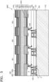
- FIG. 1 is a schematic cross-sectional view illustrating a display apparatus 100 according to an example not forming part of the present invention.
- each of the pixels may be one unit for displaying images.
- Each of the pixels may include subpixels emitting different colors. Images may be displayed by controlling colors and the amounts of light emitted by the subpixels.
- each of the pixels may include a first subpixel SP1, a second subpixel SP2, and a third subpixel SP3.
- the display apparatus 100 may include a substrate 110, a driving layer 130 provided on the substrate 110, and a light-emitting resonance layer LR provided on the driving layer 130.
- the substrate 110 may be a substrate for supporting the driving layer 130 thereon.
- the substrate 110 may not be a growth substrate.
- a silicon substrate, a glass substrate, a sapphire substrate, or a silicon substrate coated with silicon oxide (SiO 2 ) may be used as the substrate 110.
- SiO 2 silicon oxide
- the substrate 110 may be a substrate used for a complementary metal-oxide semiconductor (CMOS) backplane. In this case, the substrate 110 and the driving layer 130 may form a CMOS backplane.
- CMOS complementary metal-oxide semiconductor
- the driving layer 130 may include driving elements 135 for electrically driving the light-emitting resonance layer LR.
- the driving elements 135 may include, for example, a transistor, a thin-film transistor (TFT), or a high electron-mobility-transistor (HEMT).
- the driving layer 130 may further include at least one insulating layer 132.
- the coupling layer 120 may be provided between the substrate 110 and the driving layer 130.
- the coupling layer 120 is for coupling the driving layer 130 to the substrate 110 and may include, for example, an adhesive layer, a fusion bonding layer or a direct bonding layer.
- the adhesive layer may include, for example, epoxy, spin on glass (SOG), or benzocyclobutene (BCB).
- the direct bonding layer may be formed by, for example, plasma or ion beam treatment.
- the coupling layer 120 is configured to physically bond the driving layer 130 to the substrate 110, and may bond the driving layer 130 to the substrate 110 by a bonding method that does not require electrical connection.
- the coupling layer 120 may not be provided.
- the light-emitting resonance layer LR may include a micro light-emitting diode (LED) array and a resonant structure.
- the light-emitting resonance layer LR may include first electrodes 141, a first semiconductor layer 142, an active layer 143, a second semiconductor layer 145, a second electrode 146, and a reflective layer 150.
- the first semiconductor layer 142 may include a first-type semiconductor.
- the first semiconductor layer 142 may include a p-type semiconductor.
- the first semiconductor layer 142 may include a p-type semiconductor of group III-V group, for example, p-GaN.
- the first semiconductor layer 142 may have a single-layer structure or a multilayer structure.
- the active layer 143 may be provided on an upper surface of the first semiconductor layer 142.
- the active layer 143 may generate light while electrons and holes are bound together.
- the active layer 143 may have a multi-quantum well (MQW) structure or a single-quantum well (SQW) structure.
- the active layer 143 may include a semiconductor of group III-V, for example, gallium nitride (GaN).
- the second semiconductor layer 145 may be provided on an upper surface of the active layer 143.
- the second semiconductor layer 145 may include, for example, an n-type semiconductor.
- the second semiconductor layer 145 may include a p-type semiconductor.
- the second semiconductor layer 145 may include an n-type semiconductor of group III-V, for example, n-GaN.
- the second semiconductor layer 145 may have a single-layer structure or a multilayer structure.
- the light-emitting resonance layer LR may have an isolation structure 147 such that light may be emitted from the active layer 143 in a subpixel basis.
- the light-emitting resonance layer LR may include the isolation structure 147 between neighboring subpixels.
- the isolation structure 147 may be, for example, an ion-implanted region.
- ions implanted into the ion-implanted region may include, for example, nitrogen (N) ions, boron (B) ions, argon (Ar) ions, or phosphorus (P) ions. Since no current is injected in the ion-implanted region, no light is emitted from the ion-implanted region.
- a light-emitting structure may be formed without a mesa structure.
- the isolation structure 147 may make it possible to implement a micro light-emitting device array structure without an etching process. Since an etching process is not used, smaller subpixels may be formed, and thus a higher-resolution micro light-emitting device array may be manufactured.
- the first electrodes 141 may be electrically connected to the first semiconductor layer 142, and the second electrode 146 may be electrically provided to the second semiconductor layer 145.
- the first electrodes 141 may be pixel electrodes corresponding to each subpixel, and the second electrode 146 may be a common electrode corresponding to a plurality of subpixels.
- the first semiconductor layer 142 and the second semiconductor layer 145 respectively include a p-type semiconductor and an n-type semiconductor
- the first electrode 141 and the second electrode 146 may respectively be a p-type electrode and an n-type electrode.
- the driving elements 135 may be electrically connected to the first electrodes 141, and may control power provided to the first electrodes 141. Therefore, the driving elements 135 may selectively drive, at least one of the first subpixel SP1, the second subpixel SP2, and the third subpixel SP3.
- the first electrodes 141 may include a reflective material to reflect light emitted downward from the active layer 143.
- the first electrodes 141 may include, for example, silver (Ag), gold (Au), aluminum (Al), chromium (Cr), nickel (Ni), or an alloy thereof.
- the second electrode 146 may be formed as a transparent electrode or an opaque electrode.
- the transparent electrode may include indium tin oxide (ITO), zinc oxide (ZnO), indium zinc oxide (IZO), indium gallium zinc oxide (IGZO), or the like.
- the second electrode 146 When the second electrode 146 is formed as a transparent electrode, the second electrode 146 may be arranged to cover the entirety of the second semiconductor layer 145.
- the second electrode 146 may further include window regions 149 corresponding to the active layer 143, and configured to transmit light emitted from the active layer 143.
- the reflective layer 150 may repeatedly reflect light emitted from the active layer 143 together with the first electrodes 141 such that the light may resonate.
- the reflective layer 150 may be, for example, a distributed Bragg reflector. Since light emitted from the active layer 143 resonates between the first electrodes 141 and the reflective layer 150, and then leaves the display apparatus 100, the divergence angle of a beam may be reduced. Therefore, in a high-resolution display apparatus, crosstalk between neighboring subpixels may be reduced to increase color purity.
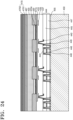
- FIG. 2 is a view illustrating a display apparatus 200 according to an example not forming part of the present invention.
- the display apparatus 200 may include a first subpixel SP1, a second subpixel SP2, and a third subpixel SP3.
- the first subpixel SP1, the second subpixel SP2, and the third subpixel SP3 may emit light having different colors.
- the display apparatus 200 may include a substrate 210, a driving layer 230 provided on the substrate 210, and a light-emitting resonance layer LR2 provided on the driving layer 230.
- the substrate 210 may not be a growth substrate, but may be a substrate for supporting the driving layer 230 thereon.
- a silicon substrate, a glass substrate, a sapphire substrate, or a silicon substrate coated with SiO 2 may be used as the substrate 210.
- substrates made of various materials may be examples of the substrate 210.
- the substrate 210 may be a substrate used for a CMOS backplane. In this case, the substrate 210 and the driving layer 230 may form a CMOS backplane.
- the driving layer 230 may include driving elements 235 for electrically driving the light-emitting resonance layer LR2 on a subpixel basis.
- the driving elements 235 may include, for example, a transistor, a TFT, or an HEMT.
- each of the driving elements 235 may include a gate electrode G, a source electrode S, and a drain electrode D.
- the driving layer 230 may further include at least one insulating layer.
- the at least one insulating layer may include a first insulating layer 231 and a second insulating layer 232.
- the second insulating layer 232 may be, for example, a gate oxide.
- a third insulating layer 237 may be further provided between the driving layer 230 and the light-emitting resonance layer LR2.
- a coupling layer 220 may be provided between the substrate 210 and the driving layer 230.
- the coupling layer 220 is configured to bond the driving layer 230 to the substrate 210, and may include, for example, an adhesive layer, a fusion bonding layer or a direct bonding layer.
- the coupling layer 220 is configured to physically bond the driving layer 230 to the substrate 210, and may bond the driving layer 230 to the substrate 210 by a bonding method that does not require electrical connection.
- the coupling layer 220 may cover the source electrodes S and the drain electrodes D during a bonding process.
- the coupling layer 220 is not limited to the thickness shown in FIG. 2 , and may have various thicknesses.
- the coupling layer 220 may have a thickness, for example, within the range of 2-5 ⁇ m.
- the light-emitting resonance layer LR2 may include a micro light-emitting device array such as a micro LED array, and a resonant structure.
- the light-emitting resonance layer LR2 may include first electrodes 241, a first semiconductor layer 242, an active layer 243, a second semiconductor layer 245, a second electrode 246, and a reflective layer 250.
- the first semiconductor layer 242 may include a first-type semiconductor.
- the first semiconductor layer 242 may include a p-type semiconductor.
- the first semiconductor layer 242 may include a p-type semiconductor of group III-V group, for example, p-GaN.
- the first semiconductor layer 242 may have a single-layer structure or a multilayer structure.
- the active layer 243 may be provided on an upper surface of the first semiconductor layer 242.
- the active layer 243 may generate light while electrons and holes are bound together.
- the active layer 243 may have a MQW structure or a SQW structure.
- the active layer 243 may include a semiconductor of group III-V, for example, GaN.
- the active layer 243 may include a two-dimensional thin film structure, or may include a three-dimensional structure such as a rod or pyramid structure.
- the second semiconductor layer 245 may be provided on an upper surface of the active layer 243.
- the second semiconductor layer 245 may include, for example, an n-type semiconductor.
- the second semiconductor layer 245 may include an n-type semiconductor of group III-V, for example, n-GaN.
- the second semiconductor layer 245 may have a single-layer structure or a multilayer structure.
- the light-emitting resonance layer LR2 may include, for example, inorganic substance-based micro LEDs.
- the micro LEDs may be provided in subpixels, respectively.
- the light-emitting resonance layer LR2 may have an isolation structure 247 such that light may be emitted from the active layer 243 in a subpixel basis.
- the active layer 243 may be arranged as discrete regions that are separated by the isolation structure 247.
- the isolation structure 247 may be, for example, an ion-implanted region. Since no current is injected in the ion-implanted region, no light is emitted from the ion-implanted region.
- the ion-implanted may be formed by implanting ions such as nitrogen ions or boron ions, and may provide insulation. In the ion-implanted region, ions may be implanted with a dose of about 10 12 ions/cm 2 to about 10 20 ions/cm 2 . However, embodiments are not limited thereto
- the first electrodes 241 may be electrically connected to the first semiconductor layer 242, and the second electrode 246 may be electrically provided to the second semiconductor layer 245.
- the first electrodes 141 may be pixel electrodes corresponding to each subpixel, and the second electrode 146 may be a common electrode corresponding to a plurality of subpixels.
- the first semiconductor layer 242 and the second semiconductor layer 245 respectively include a p-type semiconductor and an n-type semiconductor
- the first electrodes 241 may be p-type electrodes
- the second electrode 246 may be an n-type electrode.
- the driving elements 235 may be electrically connected to the first electrodes 241, and may control power provided to the first electrodes 241. Therefore, the driving elements 235 may selectively drive, at least one of the first subpixel SP1, the second subpixel SP2, and the third subpixel SP3.
- the first electrodes 241 may include a reflective material to reflect light emitted downward from the active layer 243.
- the first electrodes 241 may include, for example, silver (Ag), gold (Au), aluminum (Al), chromium (Cr), nickel (Ni), or an alloy thereof.
- the first electrodes 241, which are pixel electrodes, may independently drive the subpixels.
- the first electrodes 241 may be arranged to be spaced apart from each other and face the active layer 243.
- a current blocking layer 244 may be further provided at both lateral ends of each of the first electrodes 241.
- the current blocking layer 244 may prevent leakage of current to other adjacent subpixel areas.
- the current blocking layer 244 may include, for example, a silicon oxide or a silicon nitride.
- the current blocking layer 244 may include, for example, SiO 2 .
- the current blocking layer 244 may be provided between a lower surface of the isolation structure 247 and the first electrodes 241.
- the current blocking layer 244 may be arranged to correspond to a lower portion of the isolation structure 247.
- the third insulating layer 237 may be further provided between the driving layer 230 and the light-emitting resonance layer LR2.
- the via holes 238 may be further provided in the third insulating layer 237 to electrically connect the driving elements 235 and the first electrodes 241 to each other.
- the second electrode 246 may be formed as a transparent electrode or an opaque electrode.
- the opaque electrode may include, for example, titanium (Ti) or nickel (Ni).
- the transparent electrode may include ITO, ZnO, IZO, IGZO, or the like.
- the second electrode 246 may be arranged to cover the entirety of the second semiconductor layer 245.
- the second electrode 246 may further include window regions 249 to transmit light emitted from the active layer 243.
- the window regions 249 may be provided at positions corresponding to the active layer 243.
- the isolation structure 247 may have a predetermined thickness from the first semiconductor layer 242.
- the isolation structure 247 may have a thickness to prevent current from being injected into the second semiconductor layer 245 from the first electrodes 241. Although it is required to control current injected from the first electrodes 241 into the first semiconductor layer 242 on a subpixel basis, current may be injected into the entirety of the second semiconductor layer 245, and thus the isolation structure 247 may not be required to extend to an upper surface of the second semiconductor layer 245.
- the isolation structure 247 may have a thickness equal to or greater than the sum of the thickness of the first semiconductor layer 242 and the thickness of the active layer 243.
- the isolation structure 247 may have a thickness to provide isolation for the first semiconductor layer 242 and the second semiconductor layer 245 as well.
- the reflective layer 250 may reflect light emitted from the active layer 243. Light emitted from the active layer 243 may be repeatedly reflected and resonate between the first electrodes 241 and the reflective layer 250, and may then be extracted through the reflective layer 250. Resonating light may be output with a smaller divergence angle. Therefore, crosstalk between neighboring subpixels may be reduced.
- the reflective layer 250 may be, for example, a distributed Bragg reflector.
- reference numeral 250 used to indicate the reflective layer will also be used to indicate the distributed Bragg reflector.
- the distributed Bragg reflector 250 may be formed by alternately repeatedly stacking first layer 2501 and second layer 2502 having different refractive indexes. Due to the difference in refractive index, all waves reflected at interfaces of the first and second layers 2501 and 2502 may interfere with each other.
- the distributed Bragg reflector 250 may have a structure in which layers including two of Si, Si 3 N 4 , SiO 2 , TiO 2 , Ta 2 O 5 , and ZrO 2 are alternately stacked.
- the distributed Bragg reflector 250 may have a structure in which SiO 2 and TiO 2 layers are alternately stacked.
- the light reflectivity of the distributed Bragg reflector 250 may be controlled by adjusting the thicknesses and number of the two types of stacked layers.
- the distributed Bragg reflector 250 may have a structure in which two to five pairs of first and second layers 2501 and 2502 are stacked.
- a current spreading layer 260 may be further provided between the reflective layer 250 and the second electrode 246.
- the current spreading layer 260 may include a transparent material that transmits light.
- the current spreading layer 260 may include, for example, ITO.
- the current spreading layer 260 may increase the light emission efficiency of the active layer 243 by spreading current applied through the second electrode 246.
- a downward portion of light emitted from the active layer 243 may be reflected by the first electrodes 241 and may be directed upward, and since the isolation structure 247 does not have a mesa structure, a lateral portion of the light emitted from the active layer 243 propagates upward without being absorbed or scattered by the isolation structure 247. Therefore, light emission efficiency may be improved.
- the isolation structure 247 owing to the isolation structure 247, the size of the subpixels may be reduced, and thus the resolution of the display apparatus 200 may be increased.
- the example embodiment may have a vertical electrode structure in which the first electrodes 241 and the second electrode 246 are arranged on upper and lower sides with respect to the active layer 243.
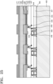
- FIG. 3 is a view illustrating a display apparatus 200A according to the present invention in which a color conversion layer is further included in the structure shown in FIG. 2 .
- components denoted with the same reference numerals as those in FIG. 2 have substantially the same functions and structures as those described with reference to FIG. 2 , and thus detailed descriptions thereof will be omitted.
- the display apparatus 200A may include the substrate 210, the driving layer 230, the light-emitting resonance layer LR2, and a color conversion layer.
- a plurality of color conversion layers 271, 272, and 273 may be provided on upper portions of the reflective layer 250 to receive light emitted from the active layer 243 and emit light having different colors.
- the active layer 243 may emit blue light.
- the active layer 243 may emit light having a different wavelength capable of exciting the color conversion layers 271, 272, and 273.
- the color conversion layers 271, 272, and 273 may respectively correspond to subpixels SP1, SP2, and SP3.
- the color conversion layers 271, 272, and 273 may include, for example, a blue conversion layer 271, a green conversion layer 272, and a red conversion layer 273.
- the blue conversion layer 271 may correspond to a blue subpixel
- the green conversion layer 272 may correspond to a green subpixel
- the red conversion layer 273 may correspond to a red subpixel.
- the blue conversion layer 271 may include, for example, a material for emitting blue light, or may be a transmission layer that transmits blue light emitted from the active layer 243.
- the blue conversion layer 271 may output blue light to the outside by transmitting blue light emitted from the active layer 243.
- the blue conversion layer 271 may further include a photoresist having good transmission characteristics or a light scattering agent.
- the green conversion layer 272 may output green light to the outside by receiving blue light emitted from the active layer 243.
- the green conversion layer 272 may include quantum dots (QDs) having a predetermined size and capable of emitting green light while being excited by blue light.
- QDs quantum dots
- the quantum dots may have a core-shell structure having a core portion and a shell portion, or may have a particle structure having no shell.
- the core-shell structure may have a single-shell or multi-shell structure.
- the multi-shell structure may be, for example, a double-shell structure.
- the quantum dots may include, for example, at least one selected from the group consisting of a group II-VI semiconductor, a group III-V semiconductor, a group IV-VI semiconductor, a group IV semiconductor, and graphene quantum dots.
- the quantum dots may include at least one selected from the group consisting of cadmium (Cd), selenium (Se), zinc (Zn), sulfur (S), and InP, but are not limited thereto.
- Each of the quantum dots may have a diameter of several tens of nanometers (nm) or less, for example, about 10 nm or less.
- the green conversion layer 272 may include a phosphor capable of emitting green light while being excited by blue light emitted from the active layer 243.
- the green conversion layer 272 may further include a photoresist having good transmission characteristics or a light scattering agent capable of uniformly outputting green light.
- the red conversion layer 273 may output red light by converting blue light emitted from the active layer 243.
- the red conversion layer 273 may include quantum dots having a predetermined size and capable of emitting red light while being excited by blue light.
- the red conversion layer 273 may include a phosphor capable of emitting red light while being excited by blue light emitted from the active layer 243.
- the red conversion layer 273 may further include a photoresist or a light scattering agent.
- the color conversion layers 271, 272, and 273 may have a cross-sectional shape having an upwardly increasing width.
- a barrier 270 may be provided between the color conversion layers 271, 272, and 273 neighboring each other.
- the barrier 270 may be formed by a black matrix for absorbing light.
- the black matrix may improve contrast by preventing or reducing crosstalk between the blue conversion layer 271, the green conversion layer 272, and the red conversion layer 273.
- each of the subpixels SP1, SP2, and SP3 of the light-emitting resonance layer LR2 may emit blue light, and the color conversion layer of each of the subpixels SP1, SP2, and SP3 may output light having a corresponding color by converting the blue light.
- the amount of light may be controlled by adjusting the amounts of current injected into the first electrodes 241 and the second electrode 246, and the color conversion layer of each subpixel may output color light, such that color images may be displayed. Even when the size of each subpixel is reduced, light leakage to neighboring subpixels may be reduced or prevented based on the isolation structure 247, thereby increasing the resolution of the display apparatus 200A.
- the divergence angle of a beam may be small, thereby reducing crosstalk between neighboring subpixels, increasing color purity, and reducing the loss of light.
- FIG. 4 is a view illustrating a display apparatus 200B according to the present invention in which color filter layers are further included in the structure shown in FIG. 3 .
- components denoted with the same reference numerals as those in FIG. 3 have substantially the same functions and structures as those described with reference to FIGS. 2 and 3 , and thus detailed descriptions thereof will be omitted.
- Color filter layers 281, 282, and 283 corresponding to upper portions of the color conversion layers 271, 272, and 273 may be provided. Each of the color filter layers 281, 282, and 283 may transmit a corresponding color. The color filter layers 281, 282, and 283 may be provided to prevent blue light emitted from the active layer 243 from being output through an unintended subpixel. The color filter layers 281, 282, and 283 may further increase color purity. A black matrix 285 may be further provided in spaces between the color filter layers 281, 282, and 283. In addition, a protective layer 287 may be further provided between the color conversion layers 271, 272, and 273 and the color filter layers 281, 282, and 283. The protective layer 287 may function as a planarization layer.
- FIG. 5 is a view illustrating a modification of the display apparatus 200 according to an example not forming part of the present invention.
- a display apparatus 200C is provided by modifying the current spreading layer 260 in the structure shown in FIG. 2 .
- components denoted with the same reference numerals as those in FIG. 2 have substantially the same functions and structures as those described with reference to FIG. 2 , and thus detailed descriptions thereof will be omitted.
- the display apparatus 200C includes a current spreading layer 2601 between the second semiconductor layer 245 and the second electrode 246.
- the current spreading layer 2601 may have a planar shape throughout the first to third subpixels SP1, SP2, and SP3.
- the current spreading layer 2601 may include a transparent material that transmits light.
- the current spreading layer 2601 may include ITO.
- FIG. 6 is a view illustrating another modification, not forming part of the present invention, of the display apparatus 200 shown in FIG. 2 .
- components denoted with the same reference numerals as those in FIG. 2 have substantially the same functions and structures as those described with reference to FIG. 2 , and thus detailed descriptions thereof will be omitted.
- a display apparatus 200D in which an active layer 2431 having a different width I is provided.
- the width I of the active layer 2431 may be less than the width N of the window regions 249 of the second electrode 246.
- the width I of the active layer 2431 may be less than a spacing C of the current blocking layer 244.
- the width N of the window regions 249 may be greater than or equal to the spacing C of the current blocking layer 244.
- the width I of the active layer 2431 may be set to be less than the width N of the window regions 249 and the spacing C of the current blocking layer 244, and thus current supplied through the first electrodes 241 and the second electrode 246 may be confined in the active layer 2431. Based on this configuration, the light emission efficiency of the active layer 2431 may be improved.
- a first semiconductor layer 2421 may also be configured to have a width less than the width N of the window regions 249 and the spacing C of the current blocking layer 244.
- FIG. 7 is a view illustrating a modification, not forming part of the present invention, of the display apparatus 200D shown in FIG. 6 .
- a display apparatus 200E is provided by removing the current spreading layer 260 from the display apparatus 200D shown in FIG. 6 .
- the second electrode 246 having the window regions 249 may be provided on the second semiconductor layer 245, and the reflective layer 250 may be provided on the second electrode 246.
- FIG. 8 is a view illustrating a modification, not forming part of the present invention, of the display apparatus 200E shown in FIG. 7 .
- a display apparatus 200F may include a second electrode 2461 having a flat plate shape.
- the second electrode 2461 may be a transparent electrode.
- the second electrode 2261 may include, for example, ITO, ZnO, IZO, IGZO, or the like.
- the second electrode 2461 may be arranged to cover the entirety of the second semiconductor layer 245.
- the reflective layer 250 may be provided on the second electrode 2461.
- the second electrode 2461 may also function as a current spreading layer.
- FIG. 9 is a view illustrating a display apparatus 300 according to another example not forming part of the present invention.
- the display apparatus 300 may include a first subpixel SP1, a second subpixel SP2, and a third subpixel SP3.
- the first subpixel SP1, the second subpixel SP2, and the third subpixel SP3 may emit light having different colors.
- the display apparatus 300 may include a substrate 310, a driving layer 330 provided on the substrate 310, and a light-emitting resonance layer LR2 provided on the driving layer 330.
- a coupling layer HB may be provided between the driving layer 330 and the light-emitting resonance layer LR2.
- the substrate 310 may include, for example, a glass substrate. However, this is merely an example, and substrates made of various materials may be examples of the substrate 310.
- the substrate 310 may be a substrate for a CMOS backplane. In this case, the substrate 310 and the driving layer 330 may form a CMOS backplane.
- the driving layer 330 may include driving elements 335 for electrically driving the light-emitting resonance layer LR2 on a subpixel basis.
- the driving elements 335 may include, for example, a transistor, a TFT, or an HEMT.
- each of the driving elements 335 may include a gate electrode G, a source electrode S, and a drain electrode D.
- the driving layer 330 may further include at least one insulating layer.
- the at least one insulating layer may include a first insulating layer 331 and a second insulating layer 332.
- the second insulating layer 332 may be, for example, a gate oxide.
- the coupling layer HB is configured to bond the driving layer 330 and the light-emitting resonance layer LR2 to each other, and may include, for example, a hybrid coupling layer.
- the coupling layer HB may be formed by a copper (Cu) damascene method.
- the coupling layer HB may include a third insulating layer 337, first bonding portions B1 provided in the third insulating layer 337, a fourth insulating layer 339, and second bonding portions B2 provided in the fourth insulating layer 339.
- the first bonding portions B1 and the second bonding portions B2 may include a conductive material.
- the first bonding portions B1 and the second bonding portions B2 may include, for example, copper (Cu).
- the driving layer 330 and the light-emitting resonance layer LR2 may be more easily bonded to each other based on the coupling layer HB. Furthermore, in the example embodiment, the substrate 310 and the driving layer 330 may be more easily manufactured by a CMOS backplane process.
- the light-emitting resonance layer LR2 may include a micro light-emitting device array such as a micro LED array, and a resonant structure.
- the light-emitting resonance layer LR2 may include first electrodes 241, a first semiconductor layer 2421, an active layer 2431, a second semiconductor layer 245, a second electrode 246, and a reflective layer 250. Since the light-emitting resonance layer LR2 has substantially the same structure as that shown in FIG. 6 , a detailed description thereof will be omitted.
- the light-emitting resonance layer LR2 may be replaced with any one of the light-emitting resonance layers LR2 described with reference to FIGS. 2 , 5 , 7 , and 8 .
- via holes 338 may be further provided in the third insulating layer 337 of the coupling layer HB.
- the via holes 338 may be electrically connected to the driving elements 335.
- the first bonding portions B1 may be connected to the via holes 338, and the first bonding portions B1 and the second bonding portions B2 may be connected to each other.
- the second bonding portions B2 may be connected to the first electrodes 241 of the light-emitting resonance layer LR2.
- the driving layer 330 and the light-emitting resonance layer LR2 may be electrically coupled to each other through the first bonding portions B1 and the second bonding portions B2.
- the display apparatus 300 may be manufactured by more easily bonding the CMOS backplane and the light-emitting resonance layer LR2 to each other.
- FIG. 10 is a graph illustrating the reflectivity of the reflective layer 250 of the display apparatus 200 shown in FIG. 2 with respect to wavelength when the reflective layer 250 is formed as a TiO 2 /SiO 2 distributed Bragg reflector (DBR).
- the reflective layer 250 has a reflectivity of about 60% when including two pairs of TiO 2 and SiO 2 layers, about 80% when including three pairs of TiO 2 and SiO 2 layers, about 95% when including five pairs of TiO 2 and SiO 2 layers, and about 100% when including ten pairs of TiO 2 and SiO 2 layers.
- FIG. 11 is a graph illustrating the light intensity of a display apparatus with respect to wavelength according to an example embodiment.
- the display apparatus of the example embodiment has a cavity thickness of about 2.45 ⁇ m, and a distributed Bragg reflector in which five pairs of TiO 2 and SiO 2 layers are stacked.
- a multi-resonance mode is shown, and the full width at half maximum is about 4.8 nm. This shows that the full width at half maximum is reduced compared to the full width at half maximum of display apparatuses of the related art which is about 19 nm. Therefore, the beam divergence angle of the display apparatus of the example embodiment may be reduced.
- the distributed Bragg reflector may have, for example, two to five pairs of stacked layers.
- display apparatuses of example embodiments are required to have a beam divergence angle similar to that of vertical cavity surface emitting lasers (VCSELs)
- the number of stacked layers of each distributed Bragg reflector may be increased.
- Display apparatuses of various example embodiments may be applied to, for example, head-up displays, virtual reality (VR) glasses, augmented reality (AR) glasses, holographic displays, or the like.
- display apparatuses of example embodiments may be applied to various other products.
- a first semiconductor layer 420, a first layer 425, and a second semiconductor layer 427 may be grown on an epitaxial substrate 410.
- the epitaxial substrate 410 may be a silicon substrate or a sapphire substrate.
- examples of the epitaxial substrate 410 are not limited thereto, and may include various other epitaxial substrates.
- the first semiconductor layer 420 may include an n-type semiconductor layer.
- the first semiconductor layer 420 may include a p-type semiconductor layer.
- the first semiconductor layer 420 may include n-type GaN.
- the first layer 425 is a layer for forming an active layer is to be formed, and may include, for example, GaN.
- a buffer layer 415 may be further formed between the epitaxial substrate 410 and the first semiconductor layer 420.
- the buffer layer 415 may include a single-layer structure or a multilayer structure, and may facilitate the growth the first semiconductor layer 420.
- the buffer layer 415 may include AIN.
- An undoped semiconductor layer such as u-GaN layer may be further provided between the buffer layer 415 and the first semiconductor layer 420.
- an isolation structure 430 may be formed in the first layer 425 and the second semiconductor layer 427 by using a mask 428.
- the mask 428 may be, for example, a mask for ion implantation.
- the isolation structure 430 may be formed by implanting ions into predetermined regions of the first layer 425 and the second semiconductor layer 427.
- the ions may include, for example, nitrogen (N) ions, boron (B) ions, argon (Ar) ions, phosphorus (P) ions, or the like. However, the ions are not limited thereto.
- the isolation structure 430 may be formed in the first layer 425 and the second semiconductor layer 427, but the thickness of the isolation structure 430 may be variously determined.
- the isolation structure 430 may be formed from the second semiconductor layer 427 to a partial depth of the first semiconductor layer 420.
- An active layer 425a and a second semiconductor layer 427a each having regions separated apart from each other by the isolation structure 430 may be formed.
- the active layer 425a and the second semiconductor layer 427a each having regions separated apart from each other may define subpixel regions.
- a micro light-emitting structure array such as a micro LED array may be formed.
- contrast may decrease because of unintended emission of light to neighboring pixels (subpixels) at pixel (subpixel) boundaries of a horizontal mesa-free structure in which pixels (subpixels) are not structurally separated from each other. According to the example embodiment, however, contrast may be improved by preventing or reducing spreading of current to adjacent pixels (subpixels) in a mesa-free isolation structure.
- a current blocking layer 433 may be deposited on the isolation structure 430.
- the current blocking layer 433 may be formed through a photoresist etching process.
- the current blocking layer 433 may include an insulating material.
- the current blocking layer 433 may electrically insulate first electrodes to be formed later.
- the current blocking layer 433 may be omitted.
- a conductive material may be deposited on the structure shown in FIG. 14 and may be etched to form first electrodes 435 separated apart from each other on a subpixel basis.
- the first electrodes 435 may be pixel electrodes operating on a subpixel basis.
- the first electrodes 435 may include a reflective conductive material.
- the first electrodes 435 may include, for example, silver (Ag), gold (Au), aluminum (Al), chromium (Cr), nickel (Ni), or an alloy thereof.
- the first electrodes 435 may be opaque electrodes.
- a first insulating layer 437 may be formed to cover the first electrodes 435.
- the first insulating layer 437 may include, but is not limited to, SiO 2 , SiN, Al 2 O 3 , TiO 2 , or the like.
- the first insulating layer 437 may be etched, and a conductive material may be deposited thereon to form via holes 440 and electrode pads 443.
- the via holes 440 may be in contact with the first electrodes 435.
- a second insulating layer 445 may be formed on the first insulating layer 437, and gate electrodes 446 may be formed on the second insulating layer 445. Thereafter, a third insulating layer 447 may be formed on the second insulating layer 445 and the gate electrodes 446. The second insulating layer 445 and the third insulating layer 447 may be etched to form source electrodes 448 and drain electrodes 449. The gate electrodes 446, the source electrodes 448, and the drain electrodes 449 may form driving elements.
- a method of forming TFTs as an example of driving elements is described.
- the source electrodes 448 may be connected to the electrode pads 443, and the drain electrodes 449 may be connected to the via holes 440. As a result, a driving layer may be formed.
- the structure illustrated in FIG. 18 may be inverted such that the epitaxial substrate 410 may be upward, and the structure may be arranged such that the third insulating layer 447 may face a substrate 450.
- the substrate 450 is a substrate for supporting the structure shown in FIG. 18 , and for example, the substrate 450 may be a silicon substrate, a glass substrate, a sapphire substrate, or a silicon substrate coated with SiO 2 .
- substrates made of various materials that are more easily bonded to the third insulating layer 447 may be examples of the substrate 450.
- the substrate 450 and the third insulating layer 447 may be bonded to each other using a coupling layer 455.
- the coupling layer 455 may include, for example, an adhesive layer, a direct coupling layer, or the like.
- the substrate 450 is for supporting the structure without electrical connection, and the substrate 450 and the structure may be physically coupled to each other by a simple bonding method.
- the coupling layer 455 may have a thickness of about 0.1 nm to about 10 ⁇ m.
- the epitaxial substrate 410 may be removed.
- the epitaxial substrate 410 may be removed by a laser lift-off method, a polishing method, or the like.
- the polishing method may be used together with a dry etching method.
- the epitaxial substrate 410 may be removed by a laser lift-off method when the epitaxial substrate 410 is a sapphire substrate, and a polishing method when the epitaxial substrate 410 is a silicon substrate.
- the polishing method may use a chemical mechanical polishing (CMP) process.
- CMP chemical mechanical polishing
- the buffer layer 415 may be optionally removed.
- FIG. 20 illustrates an example in which the buffer layer 415 is removed.
- the thickness of the first semiconductor layer 420 may be reduced by etching or polishing.
- the first semiconductor layer 420 may have a thickness of about 0.5 ⁇ m to about 3.0 ⁇ m.
- a second electrode 460 may be formed on the first semiconductor layer 420 through an etching process.
- the second electrode 460 may be formed as an opaque electrode.
- window regions 463 may be formed in the second electrode 460 by etching the second electrode 460 to allow transmission of light.
- the active layer 425a may have a width I less than or equal to the width N of the window regions 463.
- the width I of the active layer 425a may be less than or equal to the spacing C of the current blocking layer 433.
- a current spreading layer 465 may be formed on the second electrode 460.
- the current spreading layer 465 may include a transparent material.
- the current spreading layer 465 may include, for example, ITO.
- a reflective layer 470 may be formed on the current spreading layer 465.
- the reflective layer 470 may be formed as a distributed Bragg reflector.
- the reflective layer 470 may be formed by alternately stacking a plurality of pairs of third layers 4701 having a first refractive index and fourth layers 4702 having a second refractive index.
- a display apparatus may be manufactured according to the example embodiment.
- the driving layer and the light-emitting resonance layer of the display apparatus may be monolithically formed.
- a vertical electrode structure having no mesa structure may be formed through a flipping process in which the epitaxial substrate 410 is inverted to face upward.
- manufacturing processes may be simplified because a via hole etching process for forming electrodes is simplified, and a decrease in internal quantum efficiency that may be caused by a mesa structure may be prevented because no mesa structure is formed.
- the divergence angle of a beam may be reduced by inducing resonance between the first electrodes 435 and the reflective layer 470.
- FIG. 24 is a view illustrating an example, not forming part of the present invention, in which a second electrode 467 is formed as a transparent electrode unlike in FIG. 21 .
- the second electrode 467 may include, for example, ITO, ZnO, IZO, IGZO, or the like.
- the second electrode 467 may be arranged to cover the entirety of a first semiconductor layer 420.
- the transparent electrode does not need window regions because light pass through the transparent electrode.
- a reflective layer 470 may be deposited on the second electrode 467.
- the second electrode 467 may be a common electrode, and since the second electrode 467 has a simple structure, the second electrode 467 may be simply manufactured with fewer errors.
- a driving layer including TFTs is arranged under an active layer 425a, and the second electrode 467, which is a common electrode, is arranged above the active layer 425a, such that regions through which light is output may be more easily guaranteed.
- first electrodes 435 are arranged below the active layer 425a such that light emitted downward from the active layer 425a may be reflected upward by the first electrodes 435, and thus the light may be repeatedly reflected between the reflective layer 470 and the first electrodes 435, thereby inducing resonance, improving light emission efficiency, and reducing the divergence angle of a beam.
- FIGS. 25 and 26 are views illustrating a method of manufacturing a display apparatus according to another example not forming part of the present invention.
- a current spreading layer 475 may be formed on the first semiconductor layer 420 of the structure shown in FIG. 20 .
- a second electrode 477 may be formed by depositing and etching a layer on the current spreading layer 475.
- a reflective layer 470 may be formed on the second electrode 477.
- FIGS. 27 to 29 are views illustrating a method of manufacturing a display apparatus according to another example not forming part of the present invention.
- a micro LED array 500 may be formed, and a CMOS backplane 600 may be formed. Thereafter, the micro LED array 500 and the CMOS backplane 600 may be bonded together.
- the micro LED array 500 may be manufactured according to the method described with reference to FIGS. 12 to 15 . Therefore, the manufacturing method of the example embodiment will be described with the structure shown in FIG. 15 . However, the structure shown in FIG. 27 does not include the buffer layer 415 shown in FIG. 15 .
- the micro LED array 500 is prepared by inverting the structure shorn in FIG. 15 .
- a first insulating layer 510 may be formed on the first electrodes 435 of the structure shown in FIG. 15 .
- First bonding portions 512 are formed in the first insulating layer 510.
- the first bonding portions 512 may include a conductive material.
- the first bonding portions 512 may include copper (Cu).
- a damascene process may be used to form the first bonding portions 512 in the first insulating layer 510.
- the first bonding portions 512 may be formed by etching the first insulating layer 510 through a photolithography process to form holes 515, and filling copper (Cu) in the holes 515 by an electro-chemical plating technique.
- the first bonding portions 512 may be planarized by removing protruding portions of the first bonding portions 512 through a CMP process.
- CMOS backplane 600 The manufacturing process of CMOS backplane 600 is well known.
- a second insulating layer 615 is formed on a substrate 610, and gate electrodes 617 are formed on the second insulating layer 615 through photolithography and etching processes.
- a third insulating layer 620 is deposited on the second insulating layer 615. Source electrodes 623, drain electrodes 625, and electrode pads 627 are formed in the third insulating layer 620 through etching and deposition processes.
- a fourth insulating layer 630 is formed on the third insulating layer 620. Via holes 635 are formed in the fourth insulating layer 630. Thereafter, second bonding portions 640 may be formed in the fourth insulating layer 630 such that the second bonding portions 640 may be connected to the via holes 635.
- the second bonding portions 640 may include a conductive material.
- the second bonding portions 640 may include copper (Cu).
- the second bonding portions 640 may be formed in the fourth insulating layer 630 by the above-described damascene process.
- the micro LED array 500 and the CMOS backplane 600 may be formed, and as illustrated in FIG. 28 , the micro LED array 500 and the CMOS backplane 600 may be bonded together.
- the micro LED array 500 and the CMOS backplane 600 may be bonded together through a hybrid bonding process. Then, the epitaxial substrate 410 may be removed.
- a second electrode 460 may be formed on the first semiconductor layer 420 through an etching process.
- the second electrode 460 may be formed as an opaque electrode.
- window regions 463 may be formed in the second electrode 460 by etching the second electrode 460 to allow transmission of light.
- a current spreading layer 465 may be formed on the second electrode 460.
- the current spreading layer 465 may include a transparent material.
- the current spreading layer 465 may include, for example, ITO.
- a reflective layer 470 may be formed on the current spreading layer 465.
- the reflective layer 470 may be formed as a distributed Bragg reflector.
- the reflective layer 470 may be formed by alternately stacking a plurality of pairs of third layers 4701 having a first refractive index and fourth layers 4702 having a second refractive index.
- the active layer may have a width I less than or equal to the width N of the window regions 463.
- the width I of the active layer 425a may be less than or equal to the spacing C of the current blocking layer 433.
- display apparatuses may be easily manufactured through a micro LED array process, a CMOS backplane process, and a damascene process.
- high-resolution display apparatuses may be manufactured by the manufacturing methods of the example embodiments.
- the size of pixels is reduced to increase the resolution of the display apparatuses
- the beam divergence angle of the display apparatuses may be reduced by inducing resonance in a light-emitting resonance structure, thereby reducing crosstalk and increasing color purity.
- the display apparatuses are configured to reduce the divergence angle of a beam, and thus even when the pixel size of the display apparatuses is reduced for high resolution, light may not spread between neighboring pixels, thereby reducing crosstalk between neighboring pixels and increasing color purity.
- example embodiments provide methods of manufacturing display apparatuses in which a light-emitting structure and a resonant structure are coupled to each other.
Landscapes
- Engineering & Computer Science (AREA)
- Power Engineering (AREA)
- Microelectronics & Electronic Packaging (AREA)
- Computer Hardware Design (AREA)
- Manufacturing & Machinery (AREA)
- Physics & Mathematics (AREA)
- General Physics & Mathematics (AREA)
- Condensed Matter Physics & Semiconductors (AREA)
- Theoretical Computer Science (AREA)
- Geometry (AREA)
- Led Devices (AREA)
Applications Claiming Priority (1)
| Application Number | Priority Date | Filing Date | Title |
|---|---|---|---|
| KR1020190164792A KR20210073955A (ko) | 2019-12-11 | 2019-12-11 | 디스플레이 장치 및 그 제조 방법 |
Publications (2)
| Publication Number | Publication Date |
|---|---|
| EP3836212A1 EP3836212A1 (en) | 2021-06-16 |
| EP3836212B1 true EP3836212B1 (en) | 2023-04-26 |
Family
ID=73646078
Family Applications (1)
| Application Number | Title | Priority Date | Filing Date |
|---|---|---|---|
| EP20210067.3A Active EP3836212B1 (en) | 2019-12-11 | 2020-11-26 | Display apparatus and method of manufacturing the same |
Country Status (4)
| Country | Link |
|---|---|
| US (3) | US11430374B2 (ko) |
| EP (1) | EP3836212B1 (ko) |
| KR (1) | KR20210073955A (ko) |
| CN (1) | CN112951866A (ko) |
Families Citing this family (12)
| Publication number | Priority date | Publication date | Assignee | Title |
|---|---|---|---|---|
| KR20200062863A (ko) * | 2018-11-27 | 2020-06-04 | 삼성전자주식회사 | 디스플레이 장치 및 제조 방법 |
| US20220246673A1 (en) * | 2021-02-02 | 2022-08-04 | Samsung Electronics Co., Ltd. | Display module and manufacturing method thereof |
| CN114038875B (zh) * | 2021-08-04 | 2023-03-24 | 重庆康佳光电技术研究院有限公司 | 一种led芯片、显示面板及电子设备 |
| JP7423706B2 (ja) | 2021-08-20 | 2024-01-29 | ▲ナイ▼創▲顕▼示科技股▲ふん▼有限公司 | マイクロ発光ダイオード表示装置 |
| WO2023068654A1 (ko) * | 2021-10-19 | 2023-04-27 | 고려대학교 산학협력단 | 발광소자-박막트랜지스터 인테그레이션 구조 |
| US20230132423A1 (en) * | 2021-11-02 | 2023-05-04 | Nanosys, Inc. | Light emitting diode array with inactive implanted isolation regions and methods of forming the same |
| KR20230081360A (ko) * | 2021-11-30 | 2023-06-07 | 삼성전자주식회사 | 디스플레이 장치 및 그 제조 방법 |
| KR20230092393A (ko) * | 2021-12-17 | 2023-06-26 | 삼성전자주식회사 | 색 변환 필름, 디스플레이 장치 및 색 변환 필름 제조 방법 |
| WO2023142143A1 (en) * | 2022-01-31 | 2023-08-03 | Jade Bird Display (Shanghai) Company | Micro led, micro led array panel and manufacuturing method thereof |
| KR20240002279A (ko) * | 2022-06-28 | 2024-01-05 | 삼성디스플레이 주식회사 | 표시 장치 |
| CN117690946A (zh) * | 2022-09-05 | 2024-03-12 | 华为技术有限公司 | 一种MicroLED显示面板、显示设备及制造方法 |
| CN117153961B (zh) * | 2023-10-31 | 2024-02-13 | 季华实验室 | HEMT驱动MicroLED一体化背板及其制作方法 |
Family Cites Families (27)
| Publication number | Priority date | Publication date | Assignee | Title |
|---|---|---|---|---|
| US6905900B1 (en) | 2000-11-28 | 2005-06-14 | Finisar Corporation | Versatile method and system for single mode VCSELs |
| US20080299718A1 (en) * | 2007-06-01 | 2008-12-04 | Texas Instruments Incorporated | Damascene process having retained capping layer through metallization for protecting low-k dielectrics |
| US8536584B2 (en) | 2007-11-14 | 2013-09-17 | Cree, Inc. | High voltage wire bond free LEDS |
| JP2009170127A (ja) * | 2008-01-11 | 2009-07-30 | Seiko Epson Corp | 発光装置及び電子機器 |
| JP2010072529A (ja) * | 2008-09-22 | 2010-04-02 | Hitachi Displays Ltd | 液晶表示装置及びその製造方法 |
| US8642363B2 (en) * | 2009-12-09 | 2014-02-04 | Nano And Advanced Materials Institute Limited | Monolithic full-color LED micro-display on an active matrix panel manufactured using flip-chip technology |
| KR20120003775A (ko) * | 2010-07-05 | 2012-01-11 | 엘지이노텍 주식회사 | 발광 소자, 발광 소자 제조방법, 발광 소자 패키지, 및 조명 시스템 |
| KR101770585B1 (ko) * | 2010-09-03 | 2017-08-24 | 삼성전자주식회사 | 저항 어레이 및 이를 포함하는 반도체 장치 |
| US20130161667A1 (en) * | 2011-12-21 | 2013-06-27 | Phostek, Inc. | Patterned reflective layer on dielectric layer for led array |
| US9136673B2 (en) | 2012-07-20 | 2015-09-15 | The Regents Of The University Of California | Structure and method for the fabrication of a gallium nitride vertical cavity surface emitting laser |
| US8883531B2 (en) | 2012-08-28 | 2014-11-11 | Lg Display Co., Ltd. | Organic light emitting diode display device and method of manufacturing the same |
| JP6164402B2 (ja) * | 2013-03-27 | 2017-07-19 | セイコーエプソン株式会社 | 有機el装置の製造方法、および有機el装置 |
| TWI685128B (zh) * | 2013-10-16 | 2020-02-11 | 日商半導體能源研究所股份有限公司 | 發光元件、發光裝置、電子裝置及照明裝置 |
| GB201402508D0 (en) | 2014-02-13 | 2014-04-02 | Mled Ltd | Semiconductor modification process and structures |
| US10847571B2 (en) * | 2015-01-23 | 2020-11-24 | Vuereal Inc. | Micro device integration into system substrate |
| KR102354969B1 (ko) * | 2015-02-05 | 2022-01-25 | 삼성디스플레이 주식회사 | 유기 발광 디스플레이 장치 |
| JP6720747B2 (ja) * | 2016-07-19 | 2020-07-08 | 日亜化学工業株式会社 | 半導体装置、基台及びそれらの製造方法 |
| TWI674682B (zh) * | 2016-09-07 | 2019-10-11 | 優顯科技股份有限公司 | 光電半導體裝置及其製造方法 |
| TWI636562B (zh) | 2016-12-30 | 2018-09-21 | 英屬開曼群島商錼創科技股份有限公司 | 顯示裝置 |
| US10388641B2 (en) | 2017-10-19 | 2019-08-20 | Tectus Corporation | Ultra-dense LED projector |
| KR102513910B1 (ko) * | 2017-12-18 | 2023-03-23 | 엘지디스플레이 주식회사 | 전계발광 표시장치 |
| CN108597386B (zh) | 2018-01-08 | 2020-12-29 | 京东方科技集团股份有限公司 | 彩膜、微led器件及其制作方法、显示装置 |
| US11031527B2 (en) * | 2018-01-29 | 2021-06-08 | Creeled, Inc. | Reflective layers for light-emitting diodes |
| CN109148505B (zh) | 2018-08-23 | 2022-04-29 | 京东方科技集团股份有限公司 | 一种顶发射MircroLED显示面板及其制造方法 |
| WO2020073306A1 (en) * | 2018-10-12 | 2020-04-16 | Boe Technology Group Co., Ltd. | Micro light emitting diode apparatus and fabricating method thereof |
| KR20200062863A (ko) | 2018-11-27 | 2020-06-04 | 삼성전자주식회사 | 디스플레이 장치 및 제조 방법 |
| CN111384293B (zh) * | 2018-12-31 | 2023-06-09 | 乐金显示有限公司 | 发光二极管显示装置 |
-
2019
- 2019-12-11 KR KR1020190164792A patent/KR20210073955A/ko active Search and Examination
-
2020
- 2020-04-24 US US16/857,362 patent/US11430374B2/en active Active
- 2020-06-08 CN CN202010511267.2A patent/CN112951866A/zh active Pending
- 2020-11-26 EP EP20210067.3A patent/EP3836212B1/en active Active
-
2022
- 2022-04-21 US US17/725,935 patent/US11837155B2/en active Active
-
2023
- 2023-08-11 US US18/233,148 patent/US20230395016A1/en active Pending
Also Published As
| Publication number | Publication date |
|---|---|
| EP3836212A1 (en) | 2021-06-16 |
| US11837155B2 (en) | 2023-12-05 |
| US11430374B2 (en) | 2022-08-30 |
| US20210183301A1 (en) | 2021-06-17 |
| US20220246092A1 (en) | 2022-08-04 |
| KR20210073955A (ko) | 2021-06-21 |
| CN112951866A (zh) | 2021-06-11 |
| US20230395016A1 (en) | 2023-12-07 |
Similar Documents
| Publication | Publication Date | Title |
|---|---|---|
| EP3836212B1 (en) | Display apparatus and method of manufacturing the same | |
| EP3660900B1 (en) | Display apparatus and method of manufacturing the same | |
| US20220392879A1 (en) | Light emitting diode for display and display apparatus having the same | |
| US11289461B2 (en) | Light emitting device with LED stack for display and display apparatus having the same | |
| US11610939B2 (en) | Light emitting diode (LED) stack for a display | |
| US20230261033A1 (en) | Light emitting diode stack including hydrophilic material layer | |
| EP3483933B1 (en) | High resolution display device | |
| US11362073B2 (en) | Light emitting device including multiple transparent electrodes for display and display apparatus having the same | |
| US11502218B2 (en) | Display device and method of fabricating the same | |
| US11670667B2 (en) | Micro LED device and method of manufacturing the same | |
| US20220158031A1 (en) | Light emitting device for display and display apparatus having the same | |
| US20230402493A1 (en) | Micro light-emitting display apparatus and method of manufacturing the same | |
| US20220320176A1 (en) | Unit pixel for led display and led display apparatus having the same | |
| US20230106914A1 (en) | Pixel device for led display and led display apparatus having the same |
Legal Events
| Date | Code | Title | Description |
|---|---|---|---|
| PUAI | Public reference made under article 153(3) epc to a published international application that has entered the european phase |
Free format text: ORIGINAL CODE: 0009012 |
|
| STAA | Information on the status of an ep patent application or granted ep patent |
Free format text: STATUS: THE APPLICATION HAS BEEN PUBLISHED |
|
| AK | Designated contracting states |
Kind code of ref document: A1 Designated state(s): AL AT BE BG CH CY CZ DE DK EE ES FI FR GB GR HR HU IE IS IT LI LT LU LV MC MK MT NL NO PL PT RO RS SE SI SK SM TR |
|
| STAA | Information on the status of an ep patent application or granted ep patent |
Free format text: STATUS: REQUEST FOR EXAMINATION WAS MADE |
|
| 17P | Request for examination filed |
Effective date: 20211206 |
|
| RBV | Designated contracting states (corrected) |
Designated state(s): AL AT BE BG CH CY CZ DE DK EE ES FI FR GB GR HR HU IE IS IT LI LT LU LV MC MK MT NL NO PL PT RO RS SE SI SK SM TR |
|
| RIC1 | Information provided on ipc code assigned before grant |
Ipc: H01L 33/46 20100101ALI20221012BHEP Ipc: H01L 25/16 20060101ALI20221012BHEP Ipc: H01L 25/075 20060101AFI20221012BHEP |
|
| GRAP | Despatch of communication of intention to grant a patent |
Free format text: ORIGINAL CODE: EPIDOSNIGR1 |
|
| STAA | Information on the status of an ep patent application or granted ep patent |
Free format text: STATUS: GRANT OF PATENT IS INTENDED |
|
| INTG | Intention to grant announced |
Effective date: 20221222 |
|
| GRAS | Grant fee paid |
Free format text: ORIGINAL CODE: EPIDOSNIGR3 |
|
| GRAA | (expected) grant |
Free format text: ORIGINAL CODE: 0009210 |
|
| STAA | Information on the status of an ep patent application or granted ep patent |
Free format text: STATUS: THE PATENT HAS BEEN GRANTED |
|
| AK | Designated contracting states |
Kind code of ref document: B1 Designated state(s): AL AT BE BG CH CY CZ DE DK EE ES FI FR GB GR HR HU IE IS IT LI LT LU LV MC MK MT NL NO PL PT RO RS SE SI SK SM TR |
|
| REG | Reference to a national code |
Ref country code: GB Ref legal event code: FG4D |
|
| REG | Reference to a national code |
Ref country code: CH Ref legal event code: EP |
|
| REG | Reference to a national code |
Ref country code: DE Ref legal event code: R096 Ref document number: 602020010087 Country of ref document: DE |
|
| REG | Reference to a national code |
Ref country code: AT Ref legal event code: REF Ref document number: 1563458 Country of ref document: AT Kind code of ref document: T Effective date: 20230515 |
|
| REG | Reference to a national code |
Ref country code: IE Ref legal event code: FG4D |
|
| P01 | Opt-out of the competence of the unified patent court (upc) registered |
Effective date: 20230520 |
|
| REG | Reference to a national code |
Ref country code: LT Ref legal event code: MG9D |
|
| REG | Reference to a national code |
Ref country code: NL Ref legal event code: MP Effective date: 20230426 |
|
| REG | Reference to a national code |
Ref country code: AT Ref legal event code: MK05 Ref document number: 1563458 Country of ref document: AT Kind code of ref document: T Effective date: 20230426 |
|
| PG25 | Lapsed in a contracting state [announced via postgrant information from national office to epo] |
Ref country code: NL Free format text: LAPSE BECAUSE OF FAILURE TO SUBMIT A TRANSLATION OF THE DESCRIPTION OR TO PAY THE FEE WITHIN THE PRESCRIBED TIME-LIMIT Effective date: 20230426 |
|
| PG25 | Lapsed in a contracting state [announced via postgrant information from national office to epo] |
Ref country code: SE Free format text: LAPSE BECAUSE OF FAILURE TO SUBMIT A TRANSLATION OF THE DESCRIPTION OR TO PAY THE FEE WITHIN THE PRESCRIBED TIME-LIMIT Effective date: 20230426 Ref country code: PT Free format text: LAPSE BECAUSE OF FAILURE TO SUBMIT A TRANSLATION OF THE DESCRIPTION OR TO PAY THE FEE WITHIN THE PRESCRIBED TIME-LIMIT Effective date: 20230828 Ref country code: NO Free format text: LAPSE BECAUSE OF FAILURE TO SUBMIT A TRANSLATION OF THE DESCRIPTION OR TO PAY THE FEE WITHIN THE PRESCRIBED TIME-LIMIT Effective date: 20230726 Ref country code: ES Free format text: LAPSE BECAUSE OF FAILURE TO SUBMIT A TRANSLATION OF THE DESCRIPTION OR TO PAY THE FEE WITHIN THE PRESCRIBED TIME-LIMIT Effective date: 20230426 Ref country code: AT Free format text: LAPSE BECAUSE OF FAILURE TO SUBMIT A TRANSLATION OF THE DESCRIPTION OR TO PAY THE FEE WITHIN THE PRESCRIBED TIME-LIMIT Effective date: 20230426 |
|
| PG25 | Lapsed in a contracting state [announced via postgrant information from national office to epo] |
Ref country code: RS Free format text: LAPSE BECAUSE OF FAILURE TO SUBMIT A TRANSLATION OF THE DESCRIPTION OR TO PAY THE FEE WITHIN THE PRESCRIBED TIME-LIMIT Effective date: 20230426 Ref country code: PL Free format text: LAPSE BECAUSE OF FAILURE TO SUBMIT A TRANSLATION OF THE DESCRIPTION OR TO PAY THE FEE WITHIN THE PRESCRIBED TIME-LIMIT Effective date: 20230426 Ref country code: LV Free format text: LAPSE BECAUSE OF FAILURE TO SUBMIT A TRANSLATION OF THE DESCRIPTION OR TO PAY THE FEE WITHIN THE PRESCRIBED TIME-LIMIT Effective date: 20230426 Ref country code: LT Free format text: LAPSE BECAUSE OF FAILURE TO SUBMIT A TRANSLATION OF THE DESCRIPTION OR TO PAY THE FEE WITHIN THE PRESCRIBED TIME-LIMIT Effective date: 20230426 Ref country code: IS Free format text: LAPSE BECAUSE OF FAILURE TO SUBMIT A TRANSLATION OF THE DESCRIPTION OR TO PAY THE FEE WITHIN THE PRESCRIBED TIME-LIMIT Effective date: 20230826 Ref country code: HR Free format text: LAPSE BECAUSE OF FAILURE TO SUBMIT A TRANSLATION OF THE DESCRIPTION OR TO PAY THE FEE WITHIN THE PRESCRIBED TIME-LIMIT Effective date: 20230426 Ref country code: GR Free format text: LAPSE BECAUSE OF FAILURE TO SUBMIT A TRANSLATION OF THE DESCRIPTION OR TO PAY THE FEE WITHIN THE PRESCRIBED TIME-LIMIT Effective date: 20230727 |
|
| PG25 | Lapsed in a contracting state [announced via postgrant information from national office to epo] |
Ref country code: FI Free format text: LAPSE BECAUSE OF FAILURE TO SUBMIT A TRANSLATION OF THE DESCRIPTION OR TO PAY THE FEE WITHIN THE PRESCRIBED TIME-LIMIT Effective date: 20230426 |
|
| PG25 | Lapsed in a contracting state [announced via postgrant information from national office to epo] |
Ref country code: SK Free format text: LAPSE BECAUSE OF FAILURE TO SUBMIT A TRANSLATION OF THE DESCRIPTION OR TO PAY THE FEE WITHIN THE PRESCRIBED TIME-LIMIT Effective date: 20230426 |
|
| REG | Reference to a national code |
Ref country code: DE Ref legal event code: R097 Ref document number: 602020010087 Country of ref document: DE |
|
| PG25 | Lapsed in a contracting state [announced via postgrant information from national office to epo] |
Ref country code: SM Free format text: LAPSE BECAUSE OF FAILURE TO SUBMIT A TRANSLATION OF THE DESCRIPTION OR TO PAY THE FEE WITHIN THE PRESCRIBED TIME-LIMIT Effective date: 20230426 Ref country code: SK Free format text: LAPSE BECAUSE OF FAILURE TO SUBMIT A TRANSLATION OF THE DESCRIPTION OR TO PAY THE FEE WITHIN THE PRESCRIBED TIME-LIMIT Effective date: 20230426 Ref country code: RO Free format text: LAPSE BECAUSE OF FAILURE TO SUBMIT A TRANSLATION OF THE DESCRIPTION OR TO PAY THE FEE WITHIN THE PRESCRIBED TIME-LIMIT Effective date: 20230426 Ref country code: EE Free format text: LAPSE BECAUSE OF FAILURE TO SUBMIT A TRANSLATION OF THE DESCRIPTION OR TO PAY THE FEE WITHIN THE PRESCRIBED TIME-LIMIT Effective date: 20230426 Ref country code: DK Free format text: LAPSE BECAUSE OF FAILURE TO SUBMIT A TRANSLATION OF THE DESCRIPTION OR TO PAY THE FEE WITHIN THE PRESCRIBED TIME-LIMIT Effective date: 20230426 Ref country code: CZ Free format text: LAPSE BECAUSE OF FAILURE TO SUBMIT A TRANSLATION OF THE DESCRIPTION OR TO PAY THE FEE WITHIN THE PRESCRIBED TIME-LIMIT Effective date: 20230426 |
|
| PGFP | Annual fee paid to national office [announced via postgrant information from national office to epo] |
Ref country code: FR Payment date: 20231024 Year of fee payment: 4 Ref country code: DE Payment date: 20231024 Year of fee payment: 4 |
|
| PLBE | No opposition filed within time limit |
Free format text: ORIGINAL CODE: 0009261 |
|
| STAA | Information on the status of an ep patent application or granted ep patent |
Free format text: STATUS: NO OPPOSITION FILED WITHIN TIME LIMIT |
|
| 26N | No opposition filed |
Effective date: 20240129 |
|
| PG25 | Lapsed in a contracting state [announced via postgrant information from national office to epo] |
Ref country code: SI Free format text: LAPSE BECAUSE OF FAILURE TO SUBMIT A TRANSLATION OF THE DESCRIPTION OR TO PAY THE FEE WITHIN THE PRESCRIBED TIME-LIMIT Effective date: 20230426 |