EP3829272A1 - Printed circuit board - Google Patents
Printed circuit board Download PDFInfo
- Publication number
- EP3829272A1 EP3829272A1 EP19841573.9A EP19841573A EP3829272A1 EP 3829272 A1 EP3829272 A1 EP 3829272A1 EP 19841573 A EP19841573 A EP 19841573A EP 3829272 A1 EP3829272 A1 EP 3829272A1
- Authority
- EP
- European Patent Office
- Prior art keywords
- insulating substrate
- electrode
- printed circuit
- circuit board
- electrodes
- Prior art date
- Legal status (The legal status is an assumption and is not a legal conclusion. Google has not performed a legal analysis and makes no representation as to the accuracy of the status listed.)
- Granted
Links
Images




Classifications
-
- H—ELECTRICITY
- H05—ELECTRIC TECHNIQUES NOT OTHERWISE PROVIDED FOR
- H05K—PRINTED CIRCUITS; CASINGS OR CONSTRUCTIONAL DETAILS OF ELECTRIC APPARATUS; MANUFACTURE OF ASSEMBLAGES OF ELECTRICAL COMPONENTS
- H05K1/00—Printed circuits
- H05K1/02—Details
- H05K1/14—Structural association of two or more printed circuits
- H05K1/141—One or more single auxiliary printed circuits mounted on a main printed circuit, e.g. modules, adapters
-
- H—ELECTRICITY
- H05—ELECTRIC TECHNIQUES NOT OTHERWISE PROVIDED FOR
- H05K—PRINTED CIRCUITS; CASINGS OR CONSTRUCTIONAL DETAILS OF ELECTRIC APPARATUS; MANUFACTURE OF ASSEMBLAGES OF ELECTRICAL COMPONENTS
- H05K1/00—Printed circuits
- H05K1/02—Details
- H05K1/11—Printed elements for providing electric connections to or between printed circuits
- H05K1/115—Via connections; Lands around holes or via connections
-
- H—ELECTRICITY
- H05—ELECTRIC TECHNIQUES NOT OTHERWISE PROVIDED FOR
- H05K—PRINTED CIRCUITS; CASINGS OR CONSTRUCTIONAL DETAILS OF ELECTRIC APPARATUS; MANUFACTURE OF ASSEMBLAGES OF ELECTRICAL COMPONENTS
- H05K1/00—Printed circuits
- H05K1/02—Details
- H05K1/14—Structural association of two or more printed circuits
-
- H—ELECTRICITY
- H05—ELECTRIC TECHNIQUES NOT OTHERWISE PROVIDED FOR
- H05K—PRINTED CIRCUITS; CASINGS OR CONSTRUCTIONAL DETAILS OF ELECTRIC APPARATUS; MANUFACTURE OF ASSEMBLAGES OF ELECTRICAL COMPONENTS
- H05K1/00—Printed circuits
- H05K1/18—Printed circuits structurally associated with non-printed electric components
- H05K1/181—Printed circuits structurally associated with non-printed electric components associated with surface mounted components
-
- H—ELECTRICITY
- H05—ELECTRIC TECHNIQUES NOT OTHERWISE PROVIDED FOR
- H05K—PRINTED CIRCUITS; CASINGS OR CONSTRUCTIONAL DETAILS OF ELECTRIC APPARATUS; MANUFACTURE OF ASSEMBLAGES OF ELECTRICAL COMPONENTS
- H05K3/00—Apparatus or processes for manufacturing printed circuits
- H05K3/36—Assembling printed circuits with other printed circuits
- H05K3/366—Assembling printed circuits with other printed circuits substantially perpendicularly to each other
-
- H—ELECTRICITY
- H05—ELECTRIC TECHNIQUES NOT OTHERWISE PROVIDED FOR
- H05K—PRINTED CIRCUITS; CASINGS OR CONSTRUCTIONAL DETAILS OF ELECTRIC APPARATUS; MANUFACTURE OF ASSEMBLAGES OF ELECTRICAL COMPONENTS
- H05K1/00—Printed circuits
- H05K1/02—Details
- H05K1/0271—Arrangements for reducing stress or warp in rigid printed circuit boards, e.g. caused by loads, vibrations or differences in thermal expansion
-
- H—ELECTRICITY
- H05—ELECTRIC TECHNIQUES NOT OTHERWISE PROVIDED FOR
- H05K—PRINTED CIRCUITS; CASINGS OR CONSTRUCTIONAL DETAILS OF ELECTRIC APPARATUS; MANUFACTURE OF ASSEMBLAGES OF ELECTRICAL COMPONENTS
- H05K1/00—Printed circuits
- H05K1/18—Printed circuits structurally associated with non-printed electric components
-
- H—ELECTRICITY
- H05—ELECTRIC TECHNIQUES NOT OTHERWISE PROVIDED FOR
- H05K—PRINTED CIRCUITS; CASINGS OR CONSTRUCTIONAL DETAILS OF ELECTRIC APPARATUS; MANUFACTURE OF ASSEMBLAGES OF ELECTRICAL COMPONENTS
- H05K2201/00—Indexing scheme relating to printed circuits covered by H05K1/00
- H05K2201/04—Assemblies of printed circuits
- H05K2201/044—Details of backplane or midplane for mounting orthogonal PCBs
-
- H—ELECTRICITY
- H05—ELECTRIC TECHNIQUES NOT OTHERWISE PROVIDED FOR
- H05K—PRINTED CIRCUITS; CASINGS OR CONSTRUCTIONAL DETAILS OF ELECTRIC APPARATUS; MANUFACTURE OF ASSEMBLAGES OF ELECTRICAL COMPONENTS
- H05K2201/00—Indexing scheme relating to printed circuits covered by H05K1/00
- H05K2201/04—Assemblies of printed circuits
- H05K2201/048—Second PCB mounted on first PCB by inserting in window or holes of the first PCB
-
- H—ELECTRICITY
- H05—ELECTRIC TECHNIQUES NOT OTHERWISE PROVIDED FOR
- H05K—PRINTED CIRCUITS; CASINGS OR CONSTRUCTIONAL DETAILS OF ELECTRIC APPARATUS; MANUFACTURE OF ASSEMBLAGES OF ELECTRICAL COMPONENTS
- H05K2201/00—Indexing scheme relating to printed circuits covered by H05K1/00
- H05K2201/20—Details of printed circuits not provided for in H05K2201/01 - H05K2201/10
- H05K2201/2045—Protection against vibrations
Definitions
- the present invention relates to a printed circuit board including a plurality of insulating substrates.
- PTL 1 discloses a printed circuit board.
- the printed circuit board disclosed in PTL 1 includes a mother board and an auxiliary board.
- the auxiliary board is inserted into a slit provided in the mother board.
- a terminal pad provided on the mother board and a terminal pad provided on the auxiliary board are connected by solder.
- the auxiliary board perpendicularly protrudes from the mother board, and weight balance of the printed circuit board is biased to the auxiliary board side.
- vibration generated by operation of the device is transmitted to vibrate the printed circuit board.
- the weight balance of the printed circuit board is biased to the auxiliary board side as described above, vibration of the auxiliary board is amplified.
- fixing between the auxiliary board and the mother board by the solder may be released.
- An object of the present invention is to provide a printed circuit board that includes a plurality of substrates combined to be orthogonal to one another, and makes it possible to prevent vibration of a specific substrate from being amplified and to prevent fixing of the plurality of substrates by solder from being released without increasing an entire weight of the printed circuit board.
- a printed circuit board includes: a first insulating substrate having a mounting hole therein, the mounting hole penetrating through the first insulating substrate from a first surface to a second surface and having a width larger in a second direction than in a first direction orthogonal to the second direction; a second insulating substrate including a connection portion, the connection portion penetrating through the mounting hole from the first surface side and protruding from the second surface; a first electrode provided on the second surface and disposed at an edge of the mounting hole along the second direction; a second electrode provided on the connection portion and joined to the first electrode by solder; and an electronic component provided on the second surface, a center of mass of the second insulating substrate being disposed on the first surface side of the first insulating substrate, a center of mass of the electronic component being disposed on the second surface side of the first insulating substrate, the electronic component having a weight equivalent to a weight of the second insulating substrate.
- the printed circuit board of the present invention in the printed circuit board in which the plurality of substrates are combined to be orthogonal to one another, it is possible to prevent vibration of a specific substrate from being amplified and to prevent fixing of the plurality of substrates by solder from being released, without increasing the entire weight of the printed circuit board.
- Fig. 1 to Fig. 10 relate to Embodiment 1 of the present invention.
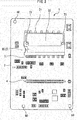
- Fig. 1 is a top view of a printed circuit board.
- Fig. 2 is a side view of the printed circuit board.
- Fig. 3 is a bottom view of the printed circuit board.
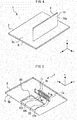
- Fig. 4 and Fig. 5 are perspective views schematically illustrating a main part of the printed circuit board.
- Fig. 6 is a bottom view schematically illustrating a main part of a first printed wiring board included in the printed circuit board.
- Fig. 7 is a front view schematically illustrating a main part of a second printed wiring board included in the printed circuit board.
- Fig. 8 is a back view schematically illustrating the main part of the second printed wiring board included in the printed circuit board.
- Fig. 9 is a cross-sectional view of the printed circuit board taken along line A-A illustrated in Fig. 5 .
- Fig. 10 is a perspective view of the printed circuit board.
- a printed circuit board 1 includes a first printed wiring board 2 and a second printed wiring board 4.
- Various kinds of electronic components 3 are mounted on the first printed wiring board 2.
- various kinds of electronic components are mounted also on the second printed wiring board 4.
- the first printed wiring board 2 is larger than the second printed wiring board 4.
- the second printed wiring board 4 is provided to be orthogonal to the first printed wiring board 2.
- an x-axis, a y-axis, and a z-axis are set as illustrated in Fig. 4 and Fig. 5 .
- the x-axis, the y-axis, and the z-axis are orthogonal to one another.
- the first printed wiring board 2 includes a first insulating substrate 6, a plurality of first electrodes 7, and a plurality of first electrodes 9.
- the first insulating substrate 6 has a plate shape with a constant thickness.
- the first insulating substrate 6 includes a first surface 6a and a second surface 6b.
- the second surface 6b is a surface directed to a direction opposite to a direction of the first surface 6a.
- the x-axis is parallel to the first surface 6a and the second surface 6b.
- the y-axis is parallel to the first surface 6a and the second surface 6b.
- the z-axis is orthogonal to the first surface 6a and the second surface 6b.
- a power module 30 is mounted on the first printed wiring board 2.
- the power module 30 is one of the various kinds of electronic components 3 described above.
- the power module 30 is provided on the second surface 6b side of the first insulating substrate 6.
- the other electronic components 3 are basically provided on the first surface 6a side. Therefore, the electronic component 3 (power module 30) is provided at least on the second surface 6b side of the first insulating substrate 6.
- the power module 30 includes a plurality of leads 31.
- the power module 30 as a kind of the electronic components 3 is mounted on the first insulating substrate 6 in such a manner that the leads 31 are inserted into the first insulating substrate 6 from the second surface 6b side.
- the leads 31 of the power module 30 are soldered at lead mounting portions 50 provided on the first surface 6a of the first insulating substrate 6.
- a heatsink 32 is provided on a top surface of the power module 30. The heatsink 32 discharges heat generated inside the power module 30, to outside of the power module 30.
- the mounting hole 15 is provided in the first insulating substrate 6.
- the mounting hole 15 is a hole to mount the second printed wiring board 4 on the first printed wiring board 2.
- the mounting hole 15 penetrates through the first insulating substrate 6 from the first surface 6a to the second surface 6b.
- the mounting hole 15 is a long hole having a width that is larger in the y-axis direction than in the x-axis direction.
- the first printed wiring board 2 includes nine first electrodes 7 is described.
- the number of first electrodes 7 included in the first printed wiring board 2 is not limited to nine.
- the first electrodes 7 are denoted by reference numerals 7a to 7i to individually specify the first electrodes 7.
- the first electrodes 7a to 7i are provided on the second surface 6b of the first insulating substrate 6.
- the first electrodes 7a to 7i configure a part of a printed circuit provided on the first insulating substrate 6.
- the first electrodes 7a to 7i are arranged in a straight line in the y-axis direction.
- the first electrodes 7a to 7i are arranged at an edge of the mounting hole 15.
- the first electrode 7a is disposed at an end among the first electrodes 7a to 7i arranged in a line.
- the first electrode 7b is adjacent to the first electrode 7a.
- the first electrode 7c is adjacent to the first electrode 7b.
- the first electrode 7h is adjacent to the first electrode 7g.
- the first electrode 7i is adjacent to the first electrode 7h.
- the first electrode 7i is disposed at an end among the first electrodes 7a and 7i arranged in a line.
- the first printed wiring board 2 includes nine first electrodes 9 is described.
- the number of first electrodes 9 included in the first printed wiring board 2 is not limited to nine.
- the first electrodes 9 are denoted by reference numerals 9a to 9i to individually specify the first electrodes 9.
- the first electrodes 9a to 9i are provided on the second surface 6b of the first insulating substrate 6.
- the first electrodes 9a to 9i configure a part of the printed circuit provided on the first insulating substrate 6.
- the first electrodes 9a to 9i are arranged in a straight line in the y-axis direction.
- the first electrodes 9a to 9i are arranged at an edge of the mounting hole 15.
- the first electrodes 9a to 9i are arranged to respectively face the first electrodes 7a to 7i with the mounting hole 15 in between.
- the first electrode 9a is disposed at an end among the first electrodes 9a to 9i arranged in a line.
- the first electrode 9a is disposed to face the first electrode 7a with the mounting hole 15 in between.
- the first electrode 9b is adjacent to the first electrode 9a.
- the first electrode 9b is disposed to face the first electrode 7b with the mounting hole 15 in between.
- the first electrode 9h is adjacent to the first electrode 9g.
- the first electrode 9h is disposed to face the first electrode 7h with the mounting hole 15 in between.
- the first electrode 9i is adjacent to the first electrode 9h.
- the first electrode 9i is disposed to face the first electrode 7i with the mounting hole 15 in between.
- the first electrode 9i is disposed at an end among the first electrodes 9a to 9i arranged in a line.
- Fig. 7 and Fig. 8 are diagrams illustrating an example of the second printed wiring board 4.
- the second printed wiring board 4 includes a second insulating substrate 18, a plurality of second electrodes 19, and a plurality of second electrodes 25.
- the second insulating substrate 18 has a plate shape with a constant thickness.
- the second insulating substrate 18 includes a surface 18a and a surface 18b.
- Fig. 7 is a diagram illustrating the second printed wiring board 4 as viewed from the surface 18a side of the second insulating substrate 18.
- the electronic components of the second printed wiring board 4 are disposed on, for example, the surface 18a side.
- the surface 18b is a surface directed to a direction opposite to a direction of the surface 18a.
- the y-axis is parallel to the surface 18a and the surface 18b.
- the z-axis is parallel to the surface 18a and the surface 18b.
- the x-axis is orthogonal to the surface 18a and the surface 18b.
- the second insulating substrate 18 includes a connection portion 23.
- the connection portion 23 is provided at one end of the second insulating substrate 18.
- the connection portion 23 penetrates through the mounting hole 15 from the first surface 6a side, and protrudes from the second surface 6b of the first insulating substrate 6.
- the second printed wiring board 4 includes nine second electrodes 19 is described.
- the number of second electrodes 19 included in the second printed wiring board 4 is not limited to nine.
- the second electrodes 19 are denoted by reference numerals 19a to 19i to individually specify the second electrodes 19.
- the second electrodes 19a to 19i are provided on the surface 18a of the second insulating substrate 18. More specifically, the second electrodes 19a to 19i are provided on the surface 18a of the connection portion 23.
- the second electrodes 19a to 19i configure a part of a printed circuit provided on the second insulating substrate 18.
- the second electrodes 19a to 19i are arranged in a straight line in the y-axis direction.
- the second electrodes 19a to 19i are arranged at an edge of the second insulating substrate 18.
- the second electrode 19a is disposed at an end among the second electrodes 19a to 19i arranged in a line.
- the second electrode 19b is adjacent to the second electrode 19a.
- the second electrode 19c is adjacent to the second electrode 19b.
- the second electrode 19h is adjacent to the second electrode 19g.
- the second electrode 19i is adjacent to the second electrode 19h.
- the second electrode 19i is disposed at an end among the second electrodes 19a to 19i arranged in a line.
- Fig. 8 is a diagram illustrating the second printed wiring board 4 as viewed from the surface 18b side that is a rear surface of the surface 18a.
- a configuration on the surface 18b side is similar to the configuration on the surface 18a side.
- the second printed wiring board 4 includes the plurality of second electrodes 25.
- the second printed wiring board 4 includes nine second electrodes 25.
- the number of second electrodes 25 included in the second printed wiring board 4 is not limited to nine.
- the second electrodes 25 are denoted by reference numerals 25a to 25i to individually specify the second electrodes 25.
- the second electrodes 25a to 25i are provided on the surface 18b of the second insulating substrate 18. More specifically, the second electrodes 25a to 25i are provided on the surface 18b of the connection portion 23.
- the second electrodes 25a to 25i configure a part of the printed circuit provided on the second insulating substrate 18.
- the second electrodes 25a to 25i are arranged in a straight line in the y-axis direction.
- the second electrodes 25a to 25i are arranged at an edge of the second insulating substrate 18.
- the second electrode 25a is disposed at an end among the second electrodes 25a to 25i arranged in a line.
- the second electrode 25b is adjacent to the second electrode 25a.
- the second electrode 25h is adjacent to the second electrode 25g.
- the second electrode 25i is adjacent to the second electrode 25h.
- the second electrode 25i is disposed at an end among the second electrodes 25a to 25i arranged in a line.
- the printed circuit board 1 is configured in the following manner by the first printed wiring board 2 and the second printed wiring board 4 having the above-described configurations.
- the second printed wiring board 4 is disposed to be orthogonal to the first printed wiring board 2.
- the connection portion 23 is inserted into the mounting hole 15 from the first surface 6a side, and is protruded from the second surface 6b of the first insulating substrate 6.
- Fig. 9 is a diagram illustrating a cross-section taken along line A-A in Fig. 5 .
- the first electrode 7a is provided on the second surface 6b of the first insulating substrate 6.
- the second electrode 19a is disposed to be adjacent to the first electrode 7a provided on the first insulating substrate 6.
- solder 24 is provided between the second electrode 19a and the first electrode 7a. The second electrode 19a is joined to the first electrode 7a by the solder 24.
- the second electrode 19b is disposed to be adjacent to the first electrode 7b.
- a cross-section including the second electrode 19b and the first electrode 7b is similar to the cross-section illustrated in Fig. 9 .
- the solder 24 is provided between the second electrode 19b and the first electrode 7b.
- the second electrode 19b is joined to the first electrode 7b by the solder 24. Note that the second electrode 19b and the second electrode 19a are not connected by the solder 24. Further, the first electrode 7b and the first electrode 7a are not connected by the solder 24.
- the other second electrodes 19c to 19i are respectively joined to the first electrodes 7c to 7i by the solder in a similar manner.
- the second electrodes 25a to 25i of the second insulating substrate 18 are disposed to be respectively adjacent to the first electrodes 9a to 9i provided on the first insulating substrate 6. More specifically, for example, the second electrode 25a is disposed to be adjacent to the first electrode 9a provided on the first insulating substrate 6. As illustrated in Fig. 9 , solder 29 is provided between the second electrode 25a and the first electrode 9a. The second electrode 25a is joined to the first electrode 9a by the solder 29. As illustrated in Fig. 9 , the first electrode 9a is provided on the second surface 6b of the first insulating substrate 6.
- the second electrode 25b is disposed to be adjacent to the first electrode 9b.
- a cross-section including the second electrode 25b and the first electrode 9b is similar to the cross-section illustrated in Fig. 9 .
- the solder 29 is provided between the second electrode 25b and the first electrode 9b.
- the second electrode 25b is joined to the first electrode 9b by the solder 29. Note that the second electrode 25b and the second electrode 25a are not connected by the solder 29.
- the first electrode 9b and the first electrode 9a are not connected by the solder 29.
- the other second electrodes 25c to 25i are respectively joined to the first electrodes 9c to 9i by the solder in a similar manner.
- the first insulating substrate 6 includes the mounting hole 15.
- the second direction is orthogonal to the first direction.
- the mounting hole 15 is a long hole having a width that is larger in the second direction than in the first direction.
- the first electrodes 7 and the first electrodes 9 provided on the second surface 6b of the first insulating substrate 6 are arranged at the edge of the mounting hole 15 along the x-axis direction, namely, along the second direction.
- the second printed wiring board 4 is disposed to be orthogonal to the first printed wiring board 2.
- the connection portion 23 is inserted into the mounting hole 15 from the first surface 6a side, and is protruded from the second surface 6b of the first insulating substrate 6.
- the second surface 6b is directed downward, and the first printed wiring board 2 is fixed to a conveyance device of a flow soldering apparatus.
- the second printed wiring board 4 is disposed in a state standing on the first printed wiring board 2 such that the connection portion 23 protrudes downward from the first printed wiring board 2.
- molten solder is jetted upward from a nozzle.
- the first printed wiring board 2 and the second printed wiring board 4 supported by the first printed wiring board 2 are conveyed by the conveyance device, and pass across above the nozzle.
- a bottom surface of the first printed wiring board 2 is immersed in the molten solder jetted from the nozzle.
- a portion of the second printed wiring board 4 protruding from the bottom surface of the first printed wiring board 2 is immersed in the molten solder jetted from the nozzle.
- the first printed wiring board 2 is disposed such that the first electrode 7a is immersed in the molten solder from the nozzle before the first electrode 7i.
- the first printed wiring board 2 is conveyed by the conveyance device in a-y-direction. Therefore, the first electrode 7i is immersed in the molten solder next to the first electrode 7h.
- the second printed wiring board 4 is disposed such that the second electrode 19a is immersed in the molten solder from the nozzle before the second electrode 19i. Therefore, the second electrode 19i is immersed in the molten solder next to the second electrode 19h.
- the solder 24 is provided between the first electrode 7a and the second electrode 19a.
- the solder 24 is provided between the first electrode 7h and the second electrode 19h.
- the solder 24 is provided between the first electrode 7i and the second electrode 19i.
- the solder 29 is provided between the first electrode 9a and the second electrode 25a.
- the solder 29 is provided between the first electrode 9h and the second electrode 25h.
- the solder 29 is provided between the first electrode 9i and the second electrode 25i.
- the first insulating substrate 6 of the first printed wiring board 2 has a rectangular shape in plan view.
- Substrate mounting holes 60 are provided at three of four corners of the rectangular shape.
- a mold resin of the power module 30 includes module mounting holes 33.
- the power module 30 includes two module mounting holes 33.
- through holes 41 are provided in the first insulating substrate 6 at portions facing the respective module mounting holes 33. A diameter of each of the through holes 41 is larger than a diameter of each of the module mounting holes 33.
- screws 42 are fastened to screw holes or the like at a mounting position of the printed circuit board 1 after the screws 42 are inserted into the module mounting holes 33 from the through holes 41 side.
- unillustrated screws are fastened to screw holes or the like at the mounting position after the screws are inserted into the substrate mounting holes 60.
- the printed circuit board 1 is mounted by at least the screws 42 that are fastening means inserted into the module mounting holes 33.
- the printed circuit board 1 is mounted with a control circuit of a compressor mounting device such as an outdoor unit of an air-conditioning apparatus.
- the printed circuit board 1 is mounted on and fixed to a housing of such a compressor mounting device through, for example, a bracket.
- the heatsink 32 of the power module 30 is brought into close contact with the metal bracket and the like. This makes it possible to efficiently dissipate heat generated during operation of the power module 30.
- the second insulating substrate 18 is mounted in a state perpendicularly standing on the first insulating substrate 6.
- the connection portion 23 provided at the end of the second insulating substrate 18 is disposed to penetrate through the mounting hole 15 from the first surface 6a side. Accordingly, most of the second insulating substrate 18, more precisely, a center of mass of the second insulating substrate 18 is disposed on the first surface 6a side of the first insulating substrate 6.
- the power module 30 that is a kind of the electronic components 3 is disposed on the second surface 6b side of the first insulating substrate 6. More precisely, a center of mass of the power module 30 is disposed on the second surface 6b side of the first insulating substrate 6. In other words, the second insulating substrate 18 and the power module 30 are disposed on sides opposite to each other of the first insulating substrate 6. In this configuration example, a weight of the power module 30 is equivalent to a weight of the second insulating substrate 18.
- the power module 30 as a kind of the electronic components 3 also has a function as a balance weight to adjust the weight balance with, in particular, the second insulating substrate 18 in the whole of the printed circuit board 1. Even if the weight of the power module 30 is not completely equivalent to the weight of the second insulating substrate 18, the power module 30 can function as the balance weight.
- the printed circuit board 1 is mounted on the compressor mounting device, vibration caused by operation of the compressor is transmitted to vibrate the printed circuit board 1.
- the first insulating substrate 6 is directly fixed to the housing or the like of the compressor mounting apparatus by a screw or the like, whereas the second insulating substrate 18 is fixed to the first insulating substrate 6 only by the solder.
- the second insulating substrate 18 perpendicularly protrudes from the first insulating substrate 6. Accordingly, if the weight balance of the printed circuit board 1 is biased to the second insulating substrate 18, vibration of the second insulating substrate 18 is amplified. As a result of amplification of vibration of the second insulating substrate 18, fixing between the second insulating substrate 18 and the first insulating substrate 6 by the solder may be released.
- the power module 30 also has a function as the balance weight to adjust the weight balance with, in particular, the second insulating substrate 18 in the whole of the printed circuit board 1. Accordingly, when vibration of the apparatus mounted with the printed circuit board 1 is transmitted to the printed circuit board 1, it is possible to prevent the second insulating substrate 18. Thus, it is also possible to prevent fixing between the second insulating substrate 18 and the first insulating substrate 6 by the solder from being released. Further, at this time, since it is unnecessary to provide a dedicated balance weight, the entire weight of the printed circuit board 1 is not increased.
- the power module 30 as a kind of the electronic components 3 has a rectangular shape in plan view.
- the power module 30 has the rectangular shape having a width that is larger in the y-axis direction than in the x-axis direction.
- a longitudinal direction of the power module 30 and the arrangement direction of the second insulating substrate 18 are both directed in the y-axis direction and are parallel to each other.
- the leads 31 of the power module 30 are arranged along the y-axis direction on both sides of the mold of the power module 30. Accordingly, the two lead mounting portions 50 and the mounting hole 15 are disposed to be parallel to each other along the y-axis direction.
- the width of the power module 30 in the y-axis direction is equivalent to the width of the second insulating substrate 18 in the y-axis direction.
- the second insulating substrate 18 and the power module 30 are disposed in the above-described manner, which makes it possible to further improve the weight balance of the printed circuit board 1.
- a distance (B illustrated in Fig. 2 ) between the center of mass of the second insulating substrate 18 and the first surface 6a of the first insulating substrate 6 is preferably set to be lower than or equal to a prescribed distance. More specifically, for example, the distance is preferably set to be lower than or equal to 30 mm depending on the size of each of the first insulating substrate 6 and the second insulating substrate 18.
- the present invention is usable in a printed circuit board to be provided in, for example, an outdoor unit of an air-conditioning apparatus as a compressor mounting device.
Landscapes
- Engineering & Computer Science (AREA)
- Microelectronics & Electronic Packaging (AREA)
- Manufacturing & Machinery (AREA)
- Combinations Of Printed Boards (AREA)
- Structures For Mounting Electric Components On Printed Circuit Boards (AREA)
Abstract
Description
- The present invention relates to a printed circuit board including a plurality of insulating substrates.
-
PTL 1 discloses a printed circuit board. The printed circuit board disclosed inPTL 1 includes a mother board and an auxiliary board. The auxiliary board is inserted into a slit provided in the mother board. A terminal pad provided on the mother board and a terminal pad provided on the auxiliary board are connected by solder. - [PTL 1]
JP 4314809 B2 - In the printed circuit board disclosed in
PTL 1, however the auxiliary board perpendicularly protrudes from the mother board, and weight balance of the printed circuit board is biased to the auxiliary board side. For example, in a case where the printed circuit board is mounted on a device that generates vibration during operation, such as a compressor mounting device, vibration generated by operation of the device is transmitted to vibrate the printed circuit board. At this time, since the weight balance of the printed circuit board is biased to the auxiliary board side as described above, vibration of the auxiliary board is amplified. As a result of amplification of vibration of the auxiliary board, fixing between the auxiliary board and the mother board by the solder may be released. - The present invention is made to solve such issues. An object of the present invention is to provide a printed circuit board that includes a plurality of substrates combined to be orthogonal to one another, and makes it possible to prevent vibration of a specific substrate from being amplified and to prevent fixing of the plurality of substrates by solder from being released without increasing an entire weight of the printed circuit board.
- A printed circuit board according to the present invention includes: a first insulating substrate having a mounting hole therein, the mounting hole penetrating through the first insulating substrate from a first surface to a second surface and having a width larger in a second direction than in a first direction orthogonal to the second direction; a second insulating substrate including a connection portion, the connection portion penetrating through the mounting hole from the first surface side and protruding from the second surface; a first electrode provided on the second surface and disposed at an edge of the mounting hole along the second direction; a second electrode provided on the connection portion and joined to the first electrode by solder; and an electronic component provided on the second surface, a center of mass of the second insulating substrate being disposed on the first surface side of the first insulating substrate, a center of mass of the electronic component being disposed on the second surface side of the first insulating substrate, the electronic component having a weight equivalent to a weight of the second insulating substrate.
- According to the printed circuit board of the present invention, in the printed circuit board in which the plurality of substrates are combined to be orthogonal to one another, it is possible to prevent vibration of a specific substrate from being amplified and to prevent fixing of the plurality of substrates by solder from being released, without increasing the entire weight of the printed circuit board.
-
-
Fig. 1 is a top view of a printed circuit board according to Embodiment 1 of the present invention. -
Fig. 2 is a side view of the printed circuit board according toEmbodiment 1 of the present invention. -
Fig. 3 is a bottom view of the printed circuit board according toEmbodiment 1 of the present invention. -
Fig. 4 is a perspective view schematically illustrating a main part of the printed circuit board according toEmbodiment 1 of the present invention. -
Fig. 5 is a perspective view schematically illustrating a main part of the printed circuit board according toEmbodiment 1 of the present invention. -
Fig. 6 is a bottom view schematically illustrating a main part of a first printed wiring board included in the printed circuit board according toEmbodiment 1 of the present invention. -
Fig. 7 is a front view schematically illustrating a main part of a second printed wiring board included in the printed circuit board according to Embodiment 1 of the present invention. -
Fig. 8 is a back view schematically illustrating the main part of the second printed wiring board included in the printed circuit board according toEmbodiment 1 of the present invention. -
Fig. 9 is a cross-sectional view of the printed circuit board according toEmbodiment 1 of the present invention taken along line A-A illustrated inFig. 5 -
Fig. 10 is a perspective view of the printed circuit board according toEmbodiment 1 of the present invention. - An embodiment of the present invention is described with reference to accompanying drawings. In the drawings, the same or equivalent parts are denoted by the same reference numerals, and repetitive descriptions are appropriately simplified or omitted. Note that the present invention is not limited to the following embodiment, and various modifications can be made without departing from the scope of the present invention.
-
Fig. 1 to Fig. 10 relate toEmbodiment 1 of the present invention.Fig. 1 is a top view of a printed circuit board.Fig. 2 is a side view of the printed circuit board.Fig. 3 is a bottom view of the printed circuit board.Fig. 4 and Fig. 5 are perspective views schematically illustrating a main part of the printed circuit board.Fig. 6 is a bottom view schematically illustrating a main part of a first printed wiring board included in the printed circuit board.Fig. 7 is a front view schematically illustrating a main part of a second printed wiring board included in the printed circuit board.Fig. 8 is a back view schematically illustrating the main part of the second printed wiring board included in the printed circuit board.Fig. 9 is a cross-sectional view of the printed circuit board taken along line A-A illustrated inFig. 5 .Fig. 10 is a perspective view of the printed circuit board. - For example, as illustrated in
Fig. 1 to Fig. 3 , a printedcircuit board 1 according to the present embodiment includes a first printedwiring board 2 and a second printedwiring board 4. Various kinds ofelectronic components 3 are mounted on the first printedwiring board 2. In addition, various kinds of electronic components are mounted also on the second printedwiring board 4. The first printedwiring board 2 is larger than the second printedwiring board 4. As illustrated inFig. 1 to Fig. 5 , the second printedwiring board 4 is provided to be orthogonal to the first printedwiring board 2. - To facilitate understanding, an x-axis, a y-axis, and a z-axis are set as illustrated in
Fig. 4 and Fig. 5 . The x-axis, the y-axis, and the z-axis are orthogonal to one another. - As illustrated in
Fig. 6 , the first printedwiring board 2 includes a firstinsulating substrate 6, a plurality of first electrodes 7, and a plurality offirst electrodes 9. For example, the firstinsulating substrate 6 has a plate shape with a constant thickness. As illustrated inFig. 4 to Fig. 6 , the firstinsulating substrate 6 includes afirst surface 6a and asecond surface 6b. Thesecond surface 6b is a surface directed to a direction opposite to a direction of thefirst surface 6a. The x-axis is parallel to thefirst surface 6a and thesecond surface 6b. The y-axis is parallel to thefirst surface 6a and thesecond surface 6b. The z-axis is orthogonal to thefirst surface 6a and thesecond surface 6b. - A
power module 30 is mounted on the first printedwiring board 2. Thepower module 30 is one of the various kinds ofelectronic components 3 described above. Thepower module 30 is provided on thesecond surface 6b side of the firstinsulating substrate 6. The otherelectronic components 3 are basically provided on thefirst surface 6a side. Therefore, the electronic component 3 (power module 30) is provided at least on thesecond surface 6b side of the firstinsulating substrate 6. - The
power module 30 includes a plurality of leads 31. Thepower module 30 as a kind of theelectronic components 3 is mounted on the first insulatingsubstrate 6 in such a manner that the leads 31 are inserted into the first insulatingsubstrate 6 from thesecond surface 6b side. As illustrated inFig. 1 , theleads 31 of thepower module 30 are soldered atlead mounting portions 50 provided on thefirst surface 6a of the first insulatingsubstrate 6. Further, as illustrated inFig. 3 , aheatsink 32 is provided on a top surface of thepower module 30. Theheatsink 32 discharges heat generated inside thepower module 30, to outside of thepower module 30. - The mounting
hole 15 is provided in the first insulatingsubstrate 6. The mountinghole 15 is a hole to mount the second printedwiring board 4 on the first printedwiring board 2. The mountinghole 15 penetrates through the first insulatingsubstrate 6 from thefirst surface 6a to thesecond surface 6b. The mountinghole 15 is a long hole having a width that is larger in the y-axis direction than in the x-axis direction. - In the present embodiment, an example in which the first printed
wiring board 2 includes nine first electrodes 7 is described. The number of first electrodes 7 included in the first printedwiring board 2 is not limited to nine. In the following description, the first electrodes 7 are denoted byreference numerals 7a to 7i to individually specify the first electrodes 7. Thefirst electrodes 7a to 7i are provided on thesecond surface 6b of the first insulatingsubstrate 6. Thefirst electrodes 7a to 7i configure a part of a printed circuit provided on the first insulatingsubstrate 6. - The
first electrodes 7a to 7i are arranged in a straight line in the y-axis direction. Thefirst electrodes 7a to 7i are arranged at an edge of the mountinghole 15. For example, thefirst electrode 7a is disposed at an end among thefirst electrodes 7a to 7i arranged in a line. Thefirst electrode 7b is adjacent to thefirst electrode 7a. The first electrode 7c is adjacent to thefirst electrode 7b. Likewise, thefirst electrode 7h is adjacent to the first electrode 7g. The first electrode 7i is adjacent to thefirst electrode 7h. The first electrode 7i is disposed at an end among thefirst electrodes 7a and 7i arranged in a line. - In the present embodiment, an example in which the first printed
wiring board 2 includes ninefirst electrodes 9 is described. The number offirst electrodes 9 included in the first printedwiring board 2 is not limited to nine. In the following description, thefirst electrodes 9 are denoted byreference numerals 9a to 9i to individually specify thefirst electrodes 9. Thefirst electrodes 9a to 9i are provided on thesecond surface 6b of the first insulatingsubstrate 6. Thefirst electrodes 9a to 9i configure a part of the printed circuit provided on the first insulatingsubstrate 6. - The
first electrodes 9a to 9i are arranged in a straight line in the y-axis direction. Thefirst electrodes 9a to 9i are arranged at an edge of the mountinghole 15. Thefirst electrodes 9a to 9i are arranged to respectively face thefirst electrodes 7a to 7i with the mountinghole 15 in between. For example, thefirst electrode 9a is disposed at an end among thefirst electrodes 9a to 9i arranged in a line. Thefirst electrode 9a is disposed to face thefirst electrode 7a with the mountinghole 15 in between. The first electrode 9b is adjacent to thefirst electrode 9a. The first electrode 9b is disposed to face thefirst electrode 7b with the mountinghole 15 in between. Likewise, the first electrode 9h is adjacent to thefirst electrode 9g. The first electrode 9h is disposed to face thefirst electrode 7h with the mountinghole 15 in between. The first electrode 9i is adjacent to the first electrode 9h. The first electrode 9i is disposed to face the first electrode 7i with the mountinghole 15 in between. The first electrode 9i is disposed at an end among thefirst electrodes 9a to 9i arranged in a line. -
Fig. 7 and Fig. 8 are diagrams illustrating an example of the second printedwiring board 4. As illustrated in these figures, the second printedwiring board 4 includes a second insulatingsubstrate 18, a plurality ofsecond electrodes 19, and a plurality ofsecond electrodes 25. - For example, the second insulating
substrate 18 has a plate shape with a constant thickness. The second insulatingsubstrate 18 includes asurface 18a and asurface 18b.Fig. 7 is a diagram illustrating the second printedwiring board 4 as viewed from thesurface 18a side of the second insulatingsubstrate 18. The electronic components of the second printedwiring board 4 are disposed on, for example, thesurface 18a side. Thesurface 18b is a surface directed to a direction opposite to a direction of thesurface 18a. The y-axis is parallel to thesurface 18a and thesurface 18b. The z-axis is parallel to thesurface 18a and thesurface 18b. The x-axis is orthogonal to thesurface 18a and thesurface 18b. - The second insulating
substrate 18 includes aconnection portion 23. Theconnection portion 23 is provided at one end of the second insulatingsubstrate 18. Theconnection portion 23 penetrates through the mountinghole 15 from thefirst surface 6a side, and protrudes from thesecond surface 6b of the first insulatingsubstrate 6. - In the present embodiment, an example in which the second printed
wiring board 4 includes ninesecond electrodes 19 is described. The number ofsecond electrodes 19 included in the second printedwiring board 4 is not limited to nine. In the following description, thesecond electrodes 19 are denoted byreference numerals 19a to 19i to individually specify thesecond electrodes 19. Thesecond electrodes 19a to 19i are provided on thesurface 18a of the second insulatingsubstrate 18. More specifically, thesecond electrodes 19a to 19i are provided on thesurface 18a of theconnection portion 23. Thesecond electrodes 19a to 19i configure a part of a printed circuit provided on the second insulatingsubstrate 18. - The
second electrodes 19a to 19i are arranged in a straight line in the y-axis direction. Thesecond electrodes 19a to 19i are arranged at an edge of the second insulatingsubstrate 18. For example, thesecond electrode 19a is disposed at an end among thesecond electrodes 19a to 19i arranged in a line. Thesecond electrode 19b is adjacent to thesecond electrode 19a. Thesecond electrode 19c is adjacent to thesecond electrode 19b. Thesecond electrode 19h is adjacent to thesecond electrode 19g. The second electrode 19i is adjacent to thesecond electrode 19h. The second electrode 19i is disposed at an end among thesecond electrodes 19a to 19i arranged in a line. -
Fig. 8 is a diagram illustrating the second printedwiring board 4 as viewed from thesurface 18b side that is a rear surface of thesurface 18a. In the second printedwiring board 4, a configuration on thesurface 18b side is similar to the configuration on thesurface 18a side. In other words, the second printedwiring board 4 includes the plurality ofsecond electrodes 25. - In the present embodiment, an example in which the second printed
wiring board 4 includes ninesecond electrodes 25 is described. The number ofsecond electrodes 25 included in the second printedwiring board 4 is not limited to nine. In the following description, thesecond electrodes 25 are denoted byreference numerals 25a to 25i to individually specify thesecond electrodes 25. Thesecond electrodes 25a to 25i are provided on thesurface 18b of the second insulatingsubstrate 18. More specifically, thesecond electrodes 25a to 25i are provided on thesurface 18b of theconnection portion 23. Thesecond electrodes 25a to 25i configure a part of the printed circuit provided on the second insulatingsubstrate 18. - The
second electrodes 25a to 25i are arranged in a straight line in the y-axis direction. Thesecond electrodes 25a to 25i are arranged at an edge of the second insulatingsubstrate 18. For example, thesecond electrode 25a is disposed at an end among thesecond electrodes 25a to 25i arranged in a line. Thesecond electrode 25b is adjacent to thesecond electrode 25a. Thesecond electrode 25h is adjacent to thesecond electrode 25g. Thesecond electrode 25i is adjacent to thesecond electrode 25h. Thesecond electrode 25i is disposed at an end among thesecond electrodes 25a to 25i arranged in a line. - The printed
circuit board 1 is configured in the following manner by the first printedwiring board 2 and the second printedwiring board 4 having the above-described configurations. First, the second printedwiring board 4 is disposed to be orthogonal to the first printedwiring board 2. At this time, theconnection portion 23 is inserted into the mountinghole 15 from thefirst surface 6a side, and is protruded from thesecond surface 6b of the first insulatingsubstrate 6. - In this state, as illustrated in
Fig. 5 , thesecond electrodes 19a to 19i of the second insulatingsubstrate 18 are disposed to be respectively adjacent to thefirst electrodes 7a to 7i provided on the first insulatingsubstrate 6.Fig. 9 is a diagram illustrating a cross-section taken along line A-A inFig. 5 . As illustrated inFig. 9 , thefirst electrode 7a is provided on thesecond surface 6b of the first insulatingsubstrate 6. Thesecond electrode 19a is disposed to be adjacent to thefirst electrode 7a provided on the first insulatingsubstrate 6. Further,solder 24 is provided between thesecond electrode 19a and thefirst electrode 7a. Thesecond electrode 19a is joined to thefirst electrode 7a by thesolder 24. - In addition, the
second electrode 19b is disposed to be adjacent to thefirst electrode 7b. A cross-section including thesecond electrode 19b and thefirst electrode 7b is similar to the cross-section illustrated inFig. 9 . Thesolder 24 is provided between thesecond electrode 19b and thefirst electrode 7b. Thesecond electrode 19b is joined to thefirst electrode 7b by thesolder 24. Note that thesecond electrode 19b and thesecond electrode 19a are not connected by thesolder 24. Further, thefirst electrode 7b and thefirst electrode 7a are not connected by thesolder 24. - The other
second electrodes 19c to 19i are respectively joined to the first electrodes 7c to 7i by the solder in a similar manner. - Further, in this state, the
second electrodes 25a to 25i of the second insulatingsubstrate 18 are disposed to be respectively adjacent to thefirst electrodes 9a to 9i provided on the first insulatingsubstrate 6. More specifically, for example, thesecond electrode 25a is disposed to be adjacent to thefirst electrode 9a provided on the first insulatingsubstrate 6. As illustrated inFig. 9 ,solder 29 is provided between thesecond electrode 25a and thefirst electrode 9a. Thesecond electrode 25a is joined to thefirst electrode 9a by thesolder 29. As illustrated inFig. 9 , thefirst electrode 9a is provided on thesecond surface 6b of the first insulatingsubstrate 6. - Further, the
second electrode 25b is disposed to be adjacent to the first electrode 9b. A cross-section including thesecond electrode 25b and the first electrode 9b is similar to the cross-section illustrated inFig. 9 . Thesolder 29 is provided between thesecond electrode 25b and the first electrode 9b. Thesecond electrode 25b is joined to the first electrode 9b by thesolder 29. Note that thesecond electrode 25b and thesecond electrode 25a are not connected by thesolder 29. The first electrode 9b and thefirst electrode 9a are not connected by thesolder 29. - The other
second electrodes 25c to 25i are respectively joined to thefirst electrodes 9c to 9i by the solder in a similar manner. - In the printed
circuit board 1 having the above-described configuration according toEmbodiment 1, the first insulatingsubstrate 6 includes the mountinghole 15. When the y-axis direction is defined as a first direction and the x-axis direction is defined as a second direction, the second direction is orthogonal to the first direction. The mountinghole 15 is a long hole having a width that is larger in the second direction than in the first direction. Further, the first electrodes 7 and thefirst electrodes 9 provided on thesecond surface 6b of the first insulatingsubstrate 6 are arranged at the edge of the mountinghole 15 along the x-axis direction, namely, along the second direction. - Next, a method of joining the first printed
wiring board 2 illustrated inFig. 3 having the above-described configuration and the second printedwiring board 4 illustrated inFig. 4 and Fig. 5 having the above-described configuration, by the solder is described. - First, the second printed
wiring board 4 is disposed to be orthogonal to the first printedwiring board 2. At this time, theconnection portion 23 is inserted into the mountinghole 15 from thefirst surface 6a side, and is protruded from thesecond surface 6b of the first insulatingsubstrate 6. - Next, the
second surface 6b is directed downward, and the first printedwiring board 2 is fixed to a conveyance device of a flow soldering apparatus. The second printedwiring board 4 is disposed in a state standing on the first printedwiring board 2 such that theconnection portion 23 protrudes downward from the first printedwiring board 2. In the flow soldering apparatus, molten solder is jetted upward from a nozzle. The first printedwiring board 2 and the second printedwiring board 4 supported by the first printedwiring board 2 are conveyed by the conveyance device, and pass across above the nozzle. When the first printedwiring board 2 passes above the nozzle, a bottom surface of the first printedwiring board 2 is immersed in the molten solder jetted from the nozzle. In addition, a portion of the second printedwiring board 4 protruding from the bottom surface of the first printedwiring board 2 is immersed in the molten solder jetted from the nozzle. - The first printed
wiring board 2 is disposed such that thefirst electrode 7a is immersed in the molten solder from the nozzle before the first electrode 7i. In the case of the configuration example illustrated inFig. 4 and Fig. 5 , the first printedwiring board 2 is conveyed by the conveyance device in a-y-direction. Therefore, the first electrode 7i is immersed in the molten solder next to thefirst electrode 7h. Further, the second printedwiring board 4 is disposed such that thesecond electrode 19a is immersed in the molten solder from the nozzle before the second electrode 19i. Therefore, the second electrode 19i is immersed in the molten solder next to thesecond electrode 19h. - For example, when the
first electrode 7a and thesecond electrode 19a are immersed in the molten solder from the nozzle, thesolder 24 is provided between thefirst electrode 7a and thesecond electrode 19a. Likewise, when thefirst electrode 7h and thesecond electrode 19h are immersed in the molten solder from the nozzle, thesolder 24 is provided between thefirst electrode 7h and thesecond electrode 19h. When the first electrode 7i and the second electrode 19i are immersed in the molten solder from the nozzle, thesolder 24 is provided between the first electrode 7i and the second electrode 19i. - For example, when the
first electrode 9a and thesecond electrode 25a are immersed in the molten solder from the nozzle, thesolder 29 is provided between thefirst electrode 9a and thesecond electrode 25a. Likewise, when the first electrode 9h and thesecond electrode 25h are immersed in the molten solder from the nozzle, thesolder 29 is provided between the first electrode 9h and thesecond electrode 25h. When the first electrode 9i and thesecond electrode 25i are immersed in the molten solder from the nozzle, thesolder 29 is provided between the first electrode 9i and thesecond electrode 25i. - As illustrated in
Fig. 1 andFig. 3 , the first insulatingsubstrate 6 of the first printedwiring board 2 has a rectangular shape in plan view.Substrate mounting holes 60 are provided at three of four corners of the rectangular shape. In addition, as illustrated inFig. 1 andFig. 3 , a mold resin of thepower module 30 includes module mounting holes 33. In the configuration example illustrated here, thepower module 30 includes two module mounting holes 33. Further, throughholes 41 are provided in the first insulatingsubstrate 6 at portions facing the respective module mounting holes 33. A diameter of each of the throughholes 41 is larger than a diameter of each of the module mounting holes 33. - As illustrated in
Fig. 10 , screws 42 are fastened to screw holes or the like at a mounting position of the printedcircuit board 1 after thescrews 42 are inserted into themodule mounting holes 33 from the throughholes 41 side. In addition, unillustrated screws are fastened to screw holes or the like at the mounting position after the screws are inserted into the substrate mounting holes 60. The printedcircuit board 1 is mounted by at least thescrews 42 that are fastening means inserted into the module mounting holes 33. - More specifically, for example, the printed
circuit board 1 is mounted with a control circuit of a compressor mounting device such as an outdoor unit of an air-conditioning apparatus. The printedcircuit board 1 is mounted on and fixed to a housing of such a compressor mounting device through, for example, a bracket. At this time, theheatsink 32 of thepower module 30 is brought into close contact with the metal bracket and the like. This makes it possible to efficiently dissipate heat generated during operation of thepower module 30. - In the printed
circuit board 1 having the above-described configuration, the second insulatingsubstrate 18 is mounted in a state perpendicularly standing on the first insulatingsubstrate 6. At this time, theconnection portion 23 provided at the end of the second insulatingsubstrate 18 is disposed to penetrate through the mountinghole 15 from thefirst surface 6a side. Accordingly, most of the second insulatingsubstrate 18, more precisely, a center of mass of the second insulatingsubstrate 18 is disposed on thefirst surface 6a side of the first insulatingsubstrate 6. - In contrast, the
power module 30 that is a kind of theelectronic components 3 is disposed on thesecond surface 6b side of the first insulatingsubstrate 6. More precisely, a center of mass of thepower module 30 is disposed on thesecond surface 6b side of the first insulatingsubstrate 6. In other words, the second insulatingsubstrate 18 and thepower module 30 are disposed on sides opposite to each other of the first insulatingsubstrate 6. In this configuration example, a weight of thepower module 30 is equivalent to a weight of the second insulatingsubstrate 18. - Therefore, unbalance caused by the second insulating
substrate 18 protruding to one side of the first insulatingsubstrate 6 is eliminated by thepower module 30. In other words, thepower module 30 as a kind of theelectronic components 3 also has a function as a balance weight to adjust the weight balance with, in particular, the second insulatingsubstrate 18 in the whole of the printedcircuit board 1. Even if the weight of thepower module 30 is not completely equivalent to the weight of the second insulatingsubstrate 18, thepower module 30 can function as the balance weight. - As described above, for example, in the case where the printed
circuit board 1 is mounted on the compressor mounting device, vibration caused by operation of the compressor is transmitted to vibrate the printedcircuit board 1. At this time, the first insulatingsubstrate 6 is directly fixed to the housing or the like of the compressor mounting apparatus by a screw or the like, whereas the second insulatingsubstrate 18 is fixed to the first insulatingsubstrate 6 only by the solder. In addition, the second insulatingsubstrate 18 perpendicularly protrudes from the first insulatingsubstrate 6. Accordingly, if the weight balance of the printedcircuit board 1 is biased to the second insulatingsubstrate 18, vibration of the second insulatingsubstrate 18 is amplified. As a result of amplification of vibration of the second insulatingsubstrate 18, fixing between the second insulatingsubstrate 18 and the first insulatingsubstrate 6 by the solder may be released. - In this regard, in the printed
circuit board 1 according to the present embodiment, thepower module 30 also has a function as the balance weight to adjust the weight balance with, in particular, the second insulatingsubstrate 18 in the whole of the printedcircuit board 1. Accordingly, when vibration of the apparatus mounted with the printedcircuit board 1 is transmitted to the printedcircuit board 1, it is possible to prevent the second insulatingsubstrate 18. Thus, it is also possible to prevent fixing between the second insulatingsubstrate 18 and the first insulatingsubstrate 6 by the solder from being released. Further, at this time, since it is unnecessary to provide a dedicated balance weight, the entire weight of the printedcircuit board 1 is not increased. - As illustrated in
Fig. 3 ,Fig. 5 , andFig. 6 , thepower module 30 as a kind of theelectronic components 3 has a rectangular shape in plan view. Thepower module 30 has the rectangular shape having a width that is larger in the y-axis direction than in the x-axis direction. In other words, a longitudinal direction of thepower module 30 and the arrangement direction of the second insulatingsubstrate 18 are both directed in the y-axis direction and are parallel to each other. Further, theleads 31 of thepower module 30 are arranged along the y-axis direction on both sides of the mold of thepower module 30. Accordingly, the twolead mounting portions 50 and the mountinghole 15 are disposed to be parallel to each other along the y-axis direction. - The width of the
power module 30 in the y-axis direction is equivalent to the width of the second insulatingsubstrate 18 in the y-axis direction. The second insulatingsubstrate 18 and thepower module 30 are disposed in the above-described manner, which makes it possible to further improve the weight balance of the printedcircuit board 1. - As described above, the center of mass of the second insulating
substrate 18 is disposed on thefirst surface 6a side of the first insulatingsubstrate 6. At this time, a distance (B illustrated inFig. 2 ) between the center of mass of the second insulatingsubstrate 18 and thefirst surface 6a of the first insulatingsubstrate 6 is preferably set to be lower than or equal to a prescribed distance. More specifically, for example, the distance is preferably set to be lower than or equal to 30 mm depending on the size of each of the first insulatingsubstrate 6 and the second insulatingsubstrate 18. As a result, a natural frequency of the vibration of the second insulatingsubstrate 18 with a portion where the first insulatingsubstrate 6 and the second insulatingsubstrate 18 are joined by the solder as a fixed end is increased, which makes it possible to prevent resonance with the vibration generated by operation of the compressor, and to reduce amplitude of the vibration of the second insulatingsubstrate 18. - The present invention is usable in a printed circuit board to be provided in, for example, an outdoor unit of an air-conditioning apparatus as a compressor mounting device.
-
- 1
- Printed circuit board
- 2
- First printed wiring board
- 3
- Electronic component
- 4
- Second printed wiring board
- 6
- First insulating substrate
- 6a
- First surface
- 6b
- Second surface
- 7
- First electrode
- 9
- First electrode
- 15
- Mounting hole
- 18
- Second insulating substrate
- 18a
- Surface
- 18b
- Surface
- 19
- Second electrode
- 23
- Connection portion
- 24
- Solder
- 25
- Second electrode
- 29
- Solder
- 30
- Power module
- 31
- Lead
- 32
- Heatsink
- 33
- Module mounting hole
- 41
- Hole
- 42
- Screw
- 50
- Lead mounting portion
- 60
- Substrate mounting hole
Claims (6)
- A printed circuit board, comprising:a first insulating substrate having a mounting hole therein, the mounting hole penetrating through the first insulating substrate from a first surface to a second surface and having a width larger in a second direction than in a first direction orthogonal to the second direction;a second insulating substrate including a connection portion, the connection portion penetrating through the mounting hole from the first surface side and protruding from the second surface;a first electrode provided on the second surface and disposed at an edge of the mounting hole along the second direction;a second electrode provided on the connection portion and joined to the first electrode by solder; andan electronic component provided on the second surface,a center of mass of the second insulating substrate being disposed on the first surface side of the first insulating substrate,a center of mass of the electronic component being disposed on the second surface side of the first insulating substrate,the electronic component having a weight equivalent to a weight of the second insulating substrate.
- The printed circuit board according to claim 1, wherein a distance between the center of mass of the second insulating substrate and the first surface of the first insulating substrate is lower than or equal to 30 mm.
- The printed circuit board according to claim 1 or 2, wherein the electronic component has a rectangular shape having a width that is larger in the second direction than in the first direction, in plan view.
- The printed circuit board according to claim 3, wherein the width of the electronic component in the second direction is equivalent to a width of the second insulating substrate.
- The printed circuit board according to any one of claims 1 to 4, wherein the electronic component is a power module that is mounted on the first insulating substrate by inserting leads into the first insulating substrate from the second surface side.
- The printed circuit board according to claim 5, wherein the printed circuit board is mounted by at least fastening means inserted into a module mounting hole provided in a mold resin of the power module.
Applications Claiming Priority (2)
| Application Number | Priority Date | Filing Date | Title |
|---|---|---|---|
| JP2018140332 | 2018-07-26 | ||
| PCT/JP2019/005143 WO2020021743A1 (en) | 2018-07-26 | 2019-02-13 | Printed circuit board |
Publications (3)
| Publication Number | Publication Date |
|---|---|
| EP3829272A1 true EP3829272A1 (en) | 2021-06-02 |
| EP3829272A4 EP3829272A4 (en) | 2021-09-29 |
| EP3829272B1 EP3829272B1 (en) | 2023-07-26 |
Family
ID=69180645
Family Applications (1)
| Application Number | Title | Priority Date | Filing Date |
|---|---|---|---|
| EP19841573.9A Active EP3829272B1 (en) | 2018-07-26 | 2019-02-13 | Printed circuit board |
Country Status (6)
| Country | Link |
|---|---|
| US (1) | US11432403B2 (en) |
| EP (1) | EP3829272B1 (en) |
| JP (1) | JP6573063B1 (en) |
| CN (1) | CN112425272B (en) |
| CA (1) | CA3107141C (en) |
| WO (1) | WO2020021743A1 (en) |
Families Citing this family (2)
| Publication number | Priority date | Publication date | Assignee | Title |
|---|---|---|---|---|
| JP2021111739A (en) * | 2020-01-15 | 2021-08-02 | 株式会社東芝 | Electronic apparatus |
| CN221010406U (en) * | 2023-09-28 | 2024-05-24 | 代傲阿扣基金两合公司 | Circuit board assembly and household appliance |
Family Cites Families (25)
| Publication number | Priority date | Publication date | Assignee | Title |
|---|---|---|---|---|
| JPS60147273U (en) * | 1984-03-09 | 1985-09-30 | 株式会社晃伸製機 | Livestock feeding equipment |
| JPH0642371Y2 (en) * | 1988-10-07 | 1994-11-02 | ローム株式会社 | Hybrid integrated circuit device |
| JPH0642372Y2 (en) * | 1990-08-31 | 1994-11-02 | 太陽誘電株式会社 | Hybrid integrated circuit device |
| JPH05198911A (en) * | 1992-01-20 | 1993-08-06 | Sharp Corp | Three-dimensional printed wiring board |
| JPH0569813U (en) * | 1992-02-24 | 1993-09-21 | 松下電工株式会社 | Discharge lamp lighting device |
| JPH0714971A (en) * | 1993-06-22 | 1995-01-17 | Hitachi Ltd | Semiconductor integrated circuit device |
| US5455742A (en) * | 1994-03-21 | 1995-10-03 | Eaton Corporation | Direct circuit board connection |
| JPH07307545A (en) * | 1994-05-12 | 1995-11-21 | Ibiden Co Ltd | Substrate for mounting electronic components of surface mount type and clip lead frame |
| JP2002280696A (en) * | 2001-03-15 | 2002-09-27 | Meiji Natl Ind Co Ltd | Electronic part assembly |
| JP4314809B2 (en) * | 2002-10-31 | 2009-08-19 | パナソニック電工株式会社 | Electronic device having a plurality of printed circuit boards |
| US7141937B2 (en) | 2002-10-28 | 2006-11-28 | Matsushita Electric Works, Ltd. | High-pressure discharge lamp operation device and illumination appliance having the same |
| US7154761B1 (en) * | 2004-02-13 | 2006-12-26 | Cisco Technology, Inc. | Techniques for distributing current in a backplane assembly and methods for making the same |
| US7940530B2 (en) * | 2006-10-02 | 2011-05-10 | Deere & Company | Circuit board arrangement and method of mounting circuit boards in a work machine |
| JP2008171849A (en) * | 2007-01-09 | 2008-07-24 | Funai Electric Co Ltd | Packaging structure of printed wiring board |
| JP2011044558A (en) * | 2009-08-20 | 2011-03-03 | Panasonic Electric Works Co Ltd | Circuit module and method of manufacturing the same |
| WO2012171565A1 (en) * | 2011-06-16 | 2012-12-20 | Siemens Aktiengesellschaft | Electrical contact device for connecting circuit boards |
| JP5836863B2 (en) * | 2012-03-27 | 2015-12-24 | 新電元工業株式会社 | Surface mount module, terminal of surface mount module, method of manufacturing terminal of surface mount module, and surface mount module mounting board |
| JP6321998B2 (en) * | 2013-04-04 | 2018-05-09 | エルジー イノテック カンパニー リミテッド | Lighting device |
| JP6154254B2 (en) * | 2013-09-03 | 2017-06-28 | 矢崎総業株式会社 | High-voltage / low-voltage hybrid integrated circuit |
| DE102014205385A1 (en) * | 2014-03-24 | 2015-09-24 | Robert Bosch Gmbh | Electronic module, in particular for transmission control unit, with two printed circuit board elements stacked one above the other |
| JP2017017089A (en) * | 2015-06-29 | 2017-01-19 | 三菱電機株式会社 | 3D printed circuit board |
| JP6417296B2 (en) * | 2015-08-24 | 2018-11-07 | 東芝三菱電機産業システム株式会社 | Anti-vibration fixing device for printed circuit board and power conversion device using the same |
| CN109196961B (en) * | 2016-06-08 | 2021-03-16 | 三菱电机株式会社 | The connection structure of the printed circuit board |
| JP6729147B2 (en) * | 2016-08-03 | 2020-07-22 | 三菱電機株式会社 | Printed circuit board |
| WO2019087352A1 (en) * | 2017-11-02 | 2019-05-09 | 三菱電機株式会社 | Printed circuit board assembly |
-
2019
- 2019-02-13 CA CA3107141A patent/CA3107141C/en active Active
- 2019-02-13 US US17/252,792 patent/US11432403B2/en active Active
- 2019-02-13 CN CN201980042492.1A patent/CN112425272B/en active Active
- 2019-02-13 WO PCT/JP2019/005143 patent/WO2020021743A1/en not_active Ceased
- 2019-02-13 JP JP2019533238A patent/JP6573063B1/en active Active
- 2019-02-13 EP EP19841573.9A patent/EP3829272B1/en active Active
Also Published As
| Publication number | Publication date |
|---|---|
| JP6573063B1 (en) | 2019-09-11 |
| CA3107141A1 (en) | 2020-01-30 |
| CA3107141C (en) | 2023-01-24 |
| EP3829272B1 (en) | 2023-07-26 |
| US11432403B2 (en) | 2022-08-30 |
| CN112425272A (en) | 2021-02-26 |
| JPWO2020021743A1 (en) | 2020-08-06 |
| US20210267056A1 (en) | 2021-08-26 |
| EP3829272A4 (en) | 2021-09-29 |
| WO2020021743A1 (en) | 2020-01-30 |
| CN112425272B (en) | 2024-03-01 |
Similar Documents
| Publication | Publication Date | Title |
|---|---|---|
| US6703702B2 (en) | IC chip mounting structure and display device | |
| US5615086A (en) | Apparatus for cooling a plurality of electrical components mounted on a printed circuit board | |
| US9763317B2 (en) | Method and apparatus for providing a ground and a heat transfer interface on a printed circuit board | |
| EP2046107A1 (en) | Circuit board device, electronic device provided with the circuit board device and gnd connecting method | |
| US7575443B2 (en) | Combined fastening and contacting system for electrical components on superimposed circuit boards | |
| GB2375655A (en) | Circuit board assembly | |
| CA3107141C (en) | Printed circuit board | |
| US5959840A (en) | Apparatus for cooling multiple printed circuit board mounted electrical components | |
| KR20080095415A (en) | Plasma display device | |
| JP6710601B2 (en) | Semiconductor element mounting board | |
| JP2020161547A (en) | Power converter | |
| CN102238837B (en) | Electronic apparatus | |
| KR100717748B1 (en) | Plasma display device | |
| CN210351759U (en) | Reinforced frame, structural assembly and modular device | |
| JPH0642369Y2 (en) | Printed wiring board | |
| US20080000675A1 (en) | System and method of providing structural support to printed wiring assembly components | |
| JPH03225890A (en) | Printed wiring board | |
| JP2020120131A (en) | Semiconductor element fitting substrate | |
| JP5773416B2 (en) | Circuit board | |
| JP2003243549A (en) | Electronic equipment | |
| JP2003298266A (en) | Power supply | |
| US20020180314A1 (en) | Crows foot mount | |
| JP2005109338A (en) | Substrate fitting structure | |
| JPH06310886A (en) | Electronic circuit module | |
| JP2004363610A (en) | Reinforcement board device |
Legal Events
| Date | Code | Title | Description |
|---|---|---|---|
| STAA | Information on the status of an ep patent application or granted ep patent |
Free format text: STATUS: THE INTERNATIONAL PUBLICATION HAS BEEN MADE |
|
| PUAI | Public reference made under article 153(3) epc to a published international application that has entered the european phase |
Free format text: ORIGINAL CODE: 0009012 |
|
| STAA | Information on the status of an ep patent application or granted ep patent |
Free format text: STATUS: REQUEST FOR EXAMINATION WAS MADE |
|
| 17P | Request for examination filed |
Effective date: 20210121 |
|
| AK | Designated contracting states |
Kind code of ref document: A1 Designated state(s): AL AT BE BG CH CY CZ DE DK EE ES FI FR GB GR HR HU IE IS IT LI LT LU LV MC MK MT NL NO PL PT RO RS SE SI SK SM TR |
|
| A4 | Supplementary search report drawn up and despatched |
Effective date: 20210826 |
|
| RIC1 | Information provided on ipc code assigned before grant |
Ipc: H05K 1/18 20060101ALN20210820BHEP Ipc: H05K 1/02 20060101ALN20210820BHEP Ipc: H05K 3/36 20060101ALI20210820BHEP Ipc: H05K 1/14 20060101AFI20210820BHEP |
|
| DAV | Request for validation of the european patent (deleted) | ||
| DAX | Request for extension of the european patent (deleted) | ||
| GRAP | Despatch of communication of intention to grant a patent |
Free format text: ORIGINAL CODE: EPIDOSNIGR1 |
|
| STAA | Information on the status of an ep patent application or granted ep patent |
Free format text: STATUS: GRANT OF PATENT IS INTENDED |
|
| RIC1 | Information provided on ipc code assigned before grant |
Ipc: H05K 1/18 20060101ALN20230124BHEP Ipc: H05K 1/02 20060101ALN20230124BHEP Ipc: H05K 3/36 20060101ALI20230124BHEP Ipc: H05K 1/14 20060101AFI20230124BHEP |
|
| INTG | Intention to grant announced |
Effective date: 20230209 |
|
| GRAS | Grant fee paid |
Free format text: ORIGINAL CODE: EPIDOSNIGR3 |
|
| GRAA | (expected) grant |
Free format text: ORIGINAL CODE: 0009210 |
|
| STAA | Information on the status of an ep patent application or granted ep patent |
Free format text: STATUS: THE PATENT HAS BEEN GRANTED |
|
| AK | Designated contracting states |
Kind code of ref document: B1 Designated state(s): AL AT BE BG CH CY CZ DE DK EE ES FI FR GB GR HR HU IE IS IT LI LT LU LV MC MK MT NL NO PL PT RO RS SE SI SK SM TR |
|
| REG | Reference to a national code |
Ref country code: CH Ref legal event code: EP |
|
| REG | Reference to a national code |
Ref country code: DE Ref legal event code: R096 Ref document number: 602019033733 Country of ref document: DE |
|
| REG | Reference to a national code |
Ref country code: IE Ref legal event code: FG4D |
|
| P01 | Opt-out of the competence of the unified patent court (upc) registered |
Effective date: 20230719 |
|
| REG | Reference to a national code |
Ref country code: LT Ref legal event code: MG9D |
|
| REG | Reference to a national code |
Ref country code: NL Ref legal event code: MP Effective date: 20230726 |
|
| REG | Reference to a national code |
Ref country code: AT Ref legal event code: MK05 Ref document number: 1593478 Country of ref document: AT Kind code of ref document: T Effective date: 20230726 |
|
| PG25 | Lapsed in a contracting state [announced via postgrant information from national office to epo] |
Ref country code: NL Free format text: LAPSE BECAUSE OF FAILURE TO SUBMIT A TRANSLATION OF THE DESCRIPTION OR TO PAY THE FEE WITHIN THE PRESCRIBED TIME-LIMIT Effective date: 20230726 |
|
| PG25 | Lapsed in a contracting state [announced via postgrant information from national office to epo] |
Ref country code: GR Free format text: LAPSE BECAUSE OF FAILURE TO SUBMIT A TRANSLATION OF THE DESCRIPTION OR TO PAY THE FEE WITHIN THE PRESCRIBED TIME-LIMIT Effective date: 20231027 |
|
| PG25 | Lapsed in a contracting state [announced via postgrant information from national office to epo] |
Ref country code: IS Free format text: LAPSE BECAUSE OF FAILURE TO SUBMIT A TRANSLATION OF THE DESCRIPTION OR TO PAY THE FEE WITHIN THE PRESCRIBED TIME-LIMIT Effective date: 20231126 |
|
| PG25 | Lapsed in a contracting state [announced via postgrant information from national office to epo] |
Ref country code: SE Free format text: LAPSE BECAUSE OF FAILURE TO SUBMIT A TRANSLATION OF THE DESCRIPTION OR TO PAY THE FEE WITHIN THE PRESCRIBED TIME-LIMIT Effective date: 20230726 Ref country code: RS Free format text: LAPSE BECAUSE OF FAILURE TO SUBMIT A TRANSLATION OF THE DESCRIPTION OR TO PAY THE FEE WITHIN THE PRESCRIBED TIME-LIMIT Effective date: 20230726 Ref country code: PT Free format text: LAPSE BECAUSE OF FAILURE TO SUBMIT A TRANSLATION OF THE DESCRIPTION OR TO PAY THE FEE WITHIN THE PRESCRIBED TIME-LIMIT Effective date: 20231127 Ref country code: NO Free format text: LAPSE BECAUSE OF FAILURE TO SUBMIT A TRANSLATION OF THE DESCRIPTION OR TO PAY THE FEE WITHIN THE PRESCRIBED TIME-LIMIT Effective date: 20231026 Ref country code: LV Free format text: LAPSE BECAUSE OF FAILURE TO SUBMIT A TRANSLATION OF THE DESCRIPTION OR TO PAY THE FEE WITHIN THE PRESCRIBED TIME-LIMIT Effective date: 20230726 Ref country code: LT Free format text: LAPSE BECAUSE OF FAILURE TO SUBMIT A TRANSLATION OF THE DESCRIPTION OR TO PAY THE FEE WITHIN THE PRESCRIBED TIME-LIMIT Effective date: 20230726 Ref country code: IS Free format text: LAPSE BECAUSE OF FAILURE TO SUBMIT A TRANSLATION OF THE DESCRIPTION OR TO PAY THE FEE WITHIN THE PRESCRIBED TIME-LIMIT Effective date: 20231126 Ref country code: HR Free format text: LAPSE BECAUSE OF FAILURE TO SUBMIT A TRANSLATION OF THE DESCRIPTION OR TO PAY THE FEE WITHIN THE PRESCRIBED TIME-LIMIT Effective date: 20230726 Ref country code: GR Free format text: LAPSE BECAUSE OF FAILURE TO SUBMIT A TRANSLATION OF THE DESCRIPTION OR TO PAY THE FEE WITHIN THE PRESCRIBED TIME-LIMIT Effective date: 20231027 Ref country code: FI Free format text: LAPSE BECAUSE OF FAILURE TO SUBMIT A TRANSLATION OF THE DESCRIPTION OR TO PAY THE FEE WITHIN THE PRESCRIBED TIME-LIMIT Effective date: 20230726 Ref country code: AT Free format text: LAPSE BECAUSE OF FAILURE TO SUBMIT A TRANSLATION OF THE DESCRIPTION OR TO PAY THE FEE WITHIN THE PRESCRIBED TIME-LIMIT Effective date: 20230726 |
|
| PG25 | Lapsed in a contracting state [announced via postgrant information from national office to epo] |
Ref country code: PL Free format text: LAPSE BECAUSE OF FAILURE TO SUBMIT A TRANSLATION OF THE DESCRIPTION OR TO PAY THE FEE WITHIN THE PRESCRIBED TIME-LIMIT Effective date: 20230726 |
|
| PG25 | Lapsed in a contracting state [announced via postgrant information from national office to epo] |
Ref country code: ES Free format text: LAPSE BECAUSE OF FAILURE TO SUBMIT A TRANSLATION OF THE DESCRIPTION OR TO PAY THE FEE WITHIN THE PRESCRIBED TIME-LIMIT Effective date: 20230726 |
|
| REG | Reference to a national code |
Ref country code: DE Ref legal event code: R097 Ref document number: 602019033733 Country of ref document: DE |
|
| PG25 | Lapsed in a contracting state [announced via postgrant information from national office to epo] |
Ref country code: SM Free format text: LAPSE BECAUSE OF FAILURE TO SUBMIT A TRANSLATION OF THE DESCRIPTION OR TO PAY THE FEE WITHIN THE PRESCRIBED TIME-LIMIT Effective date: 20230726 Ref country code: RO Free format text: LAPSE BECAUSE OF FAILURE TO SUBMIT A TRANSLATION OF THE DESCRIPTION OR TO PAY THE FEE WITHIN THE PRESCRIBED TIME-LIMIT Effective date: 20230726 Ref country code: ES Free format text: LAPSE BECAUSE OF FAILURE TO SUBMIT A TRANSLATION OF THE DESCRIPTION OR TO PAY THE FEE WITHIN THE PRESCRIBED TIME-LIMIT Effective date: 20230726 Ref country code: EE Free format text: LAPSE BECAUSE OF FAILURE TO SUBMIT A TRANSLATION OF THE DESCRIPTION OR TO PAY THE FEE WITHIN THE PRESCRIBED TIME-LIMIT Effective date: 20230726 Ref country code: DK Free format text: LAPSE BECAUSE OF FAILURE TO SUBMIT A TRANSLATION OF THE DESCRIPTION OR TO PAY THE FEE WITHIN THE PRESCRIBED TIME-LIMIT Effective date: 20230726 Ref country code: CZ Free format text: LAPSE BECAUSE OF FAILURE TO SUBMIT A TRANSLATION OF THE DESCRIPTION OR TO PAY THE FEE WITHIN THE PRESCRIBED TIME-LIMIT Effective date: 20230726 Ref country code: SK Free format text: LAPSE BECAUSE OF FAILURE TO SUBMIT A TRANSLATION OF THE DESCRIPTION OR TO PAY THE FEE WITHIN THE PRESCRIBED TIME-LIMIT Effective date: 20230726 |
|
| PGFP | Annual fee paid to national office [announced via postgrant information from national office to epo] |
Ref country code: GB Payment date: 20240108 Year of fee payment: 6 |
|
| PGFP | Annual fee paid to national office [announced via postgrant information from national office to epo] |
Ref country code: IT Payment date: 20240111 Year of fee payment: 6 Ref country code: FR Payment date: 20240103 Year of fee payment: 6 |
|
| PLBE | No opposition filed within time limit |
Free format text: ORIGINAL CODE: 0009261 |
|
| STAA | Information on the status of an ep patent application or granted ep patent |
Free format text: STATUS: NO OPPOSITION FILED WITHIN TIME LIMIT |
|
| 26N | No opposition filed |
Effective date: 20240429 |
|
| PG25 | Lapsed in a contracting state [announced via postgrant information from national office to epo] |
Ref country code: SI Free format text: LAPSE BECAUSE OF FAILURE TO SUBMIT A TRANSLATION OF THE DESCRIPTION OR TO PAY THE FEE WITHIN THE PRESCRIBED TIME-LIMIT Effective date: 20230726 |
|
| PG25 | Lapsed in a contracting state [announced via postgrant information from national office to epo] |
Ref country code: MC Free format text: LAPSE BECAUSE OF FAILURE TO SUBMIT A TRANSLATION OF THE DESCRIPTION OR TO PAY THE FEE WITHIN THE PRESCRIBED TIME-LIMIT Effective date: 20230726 |
|
| REG | Reference to a national code |
Ref country code: CH Ref legal event code: PL |
|
| PG25 | Lapsed in a contracting state [announced via postgrant information from national office to epo] |
Ref country code: LU Free format text: LAPSE BECAUSE OF NON-PAYMENT OF DUE FEES Effective date: 20240213 |
|
| PG25 | Lapsed in a contracting state [announced via postgrant information from national office to epo] |
Ref country code: CH Free format text: LAPSE BECAUSE OF NON-PAYMENT OF DUE FEES Effective date: 20240229 |
|
| PG25 | Lapsed in a contracting state [announced via postgrant information from national office to epo] |
Ref country code: LU Free format text: LAPSE BECAUSE OF NON-PAYMENT OF DUE FEES Effective date: 20240213 Ref country code: CH Free format text: LAPSE BECAUSE OF NON-PAYMENT OF DUE FEES Effective date: 20240229 |
|
| PG25 | Lapsed in a contracting state [announced via postgrant information from national office to epo] |
Ref country code: BG Free format text: LAPSE BECAUSE OF FAILURE TO SUBMIT A TRANSLATION OF THE DESCRIPTION OR TO PAY THE FEE WITHIN THE PRESCRIBED TIME-LIMIT Effective date: 20230726 |
|
| PG25 | Lapsed in a contracting state [announced via postgrant information from national office to epo] |
Ref country code: BG Free format text: LAPSE BECAUSE OF FAILURE TO SUBMIT A TRANSLATION OF THE DESCRIPTION OR TO PAY THE FEE WITHIN THE PRESCRIBED TIME-LIMIT Effective date: 20230726 |
|
| REG | Reference to a national code |
Ref country code: BE Ref legal event code: MM Effective date: 20240229 |
|
| PG25 | Lapsed in a contracting state [announced via postgrant information from national office to epo] |
Ref country code: BE Free format text: LAPSE BECAUSE OF NON-PAYMENT OF DUE FEES Effective date: 20240229 |
|
| PG25 | Lapsed in a contracting state [announced via postgrant information from national office to epo] |
Ref country code: IE Free format text: LAPSE BECAUSE OF NON-PAYMENT OF DUE FEES Effective date: 20240213 |
|
| PG25 | Lapsed in a contracting state [announced via postgrant information from national office to epo] |
Ref country code: IE Free format text: LAPSE BECAUSE OF NON-PAYMENT OF DUE FEES Effective date: 20240213 Ref country code: BE Free format text: LAPSE BECAUSE OF NON-PAYMENT OF DUE FEES Effective date: 20240229 |
|
| PG25 | Lapsed in a contracting state [announced via postgrant information from national office to epo] |
Ref country code: CY Free format text: LAPSE BECAUSE OF FAILURE TO SUBMIT A TRANSLATION OF THE DESCRIPTION OR TO PAY THE FEE WITHIN THE PRESCRIBED TIME-LIMIT; INVALID AB INITIO Effective date: 20190213 |
|
| PG25 | Lapsed in a contracting state [announced via postgrant information from national office to epo] |
Ref country code: HU Free format text: LAPSE BECAUSE OF FAILURE TO SUBMIT A TRANSLATION OF THE DESCRIPTION OR TO PAY THE FEE WITHIN THE PRESCRIBED TIME-LIMIT; INVALID AB INITIO Effective date: 20190213 |
|
| GBPC | Gb: european patent ceased through non-payment of renewal fee |
Effective date: 20250213 |
|
| PG25 | Lapsed in a contracting state [announced via postgrant information from national office to epo] |
Ref country code: TR Free format text: LAPSE BECAUSE OF FAILURE TO SUBMIT A TRANSLATION OF THE DESCRIPTION OR TO PAY THE FEE WITHIN THE PRESCRIBED TIME-LIMIT Effective date: 20230726 |
|
| PG25 | Lapsed in a contracting state [announced via postgrant information from national office to epo] |
Ref country code: GB Free format text: LAPSE BECAUSE OF NON-PAYMENT OF DUE FEES Effective date: 20250213 |
|
| PG25 | Lapsed in a contracting state [announced via postgrant information from national office to epo] |
Ref country code: IT Free format text: LAPSE BECAUSE OF NON-PAYMENT OF DUE FEES Effective date: 20250213 Ref country code: FR Free format text: LAPSE BECAUSE OF NON-PAYMENT OF DUE FEES Effective date: 20250228 |
|
| PGFP | Annual fee paid to national office [announced via postgrant information from national office to epo] |
Ref country code: DE Payment date: 20251230 Year of fee payment: 8 |