EP3828952A1 - Led display screen and manufacturing method therefor - Google Patents
Led display screen and manufacturing method therefor Download PDFInfo
- Publication number
- EP3828952A1 EP3828952A1 EP19841475.7A EP19841475A EP3828952A1 EP 3828952 A1 EP3828952 A1 EP 3828952A1 EP 19841475 A EP19841475 A EP 19841475A EP 3828952 A1 EP3828952 A1 EP 3828952A1
- Authority
- EP
- European Patent Office
- Prior art keywords
- led
- substrate
- display screen
- led display
- manufacturing
- Prior art date
- Legal status (The legal status is an assumption and is not a legal conclusion. Google has not performed a legal analysis and makes no representation as to the accuracy of the status listed.)
- Pending
Links
Images




Classifications
-
- H—ELECTRICITY
- H10—SEMICONDUCTOR DEVICES; ELECTRIC SOLID-STATE DEVICES NOT OTHERWISE PROVIDED FOR
- H10H—INORGANIC LIGHT-EMITTING SEMICONDUCTOR DEVICES HAVING POTENTIAL BARRIERS
- H10H29/00—Integrated devices, or assemblies of multiple devices, comprising at least one light-emitting semiconductor element covered by group H10H20/00
- H10H29/10—Integrated devices comprising at least one light-emitting semiconductor component covered by group H10H20/00
- H10H29/14—Integrated devices comprising at least one light-emitting semiconductor component covered by group H10H20/00 comprising multiple light-emitting semiconductor components
- H10H29/142—Two-dimensional arrangements, e.g. asymmetric LED layout
-
- H—ELECTRICITY
- H10—SEMICONDUCTOR DEVICES; ELECTRIC SOLID-STATE DEVICES NOT OTHERWISE PROVIDED FOR
- H10W—GENERIC PACKAGES, INTERCONNECTIONS, CONNECTORS OR OTHER CONSTRUCTIONAL DETAILS OF DEVICES COVERED BY CLASS H10
- H10W90/00—Package configurations
-
- H—ELECTRICITY
- H10—SEMICONDUCTOR DEVICES; ELECTRIC SOLID-STATE DEVICES NOT OTHERWISE PROVIDED FOR
- H10H—INORGANIC LIGHT-EMITTING SEMICONDUCTOR DEVICES HAVING POTENTIAL BARRIERS
- H10H20/00—Individual inorganic light-emitting semiconductor devices having potential barriers, e.g. light-emitting diodes [LED]
- H10H20/01—Manufacture or treatment
-
- H—ELECTRICITY
- H10—SEMICONDUCTOR DEVICES; ELECTRIC SOLID-STATE DEVICES NOT OTHERWISE PROVIDED FOR
- H10H—INORGANIC LIGHT-EMITTING SEMICONDUCTOR DEVICES HAVING POTENTIAL BARRIERS
- H10H20/00—Individual inorganic light-emitting semiconductor devices having potential barriers, e.g. light-emitting diodes [LED]
- H10H20/80—Constructional details
- H10H20/85—Packages
- H10H20/8506—Containers
-
- H—ELECTRICITY
- H10—SEMICONDUCTOR DEVICES; ELECTRIC SOLID-STATE DEVICES NOT OTHERWISE PROVIDED FOR
- H10H—INORGANIC LIGHT-EMITTING SEMICONDUCTOR DEVICES HAVING POTENTIAL BARRIERS
- H10H20/00—Individual inorganic light-emitting semiconductor devices having potential barriers, e.g. light-emitting diodes [LED]
- H10H20/80—Constructional details
- H10H20/85—Packages
- H10H20/857—Interconnections, e.g. lead-frames, bond wires or solder balls
-
- H—ELECTRICITY
- H10—SEMICONDUCTOR DEVICES; ELECTRIC SOLID-STATE DEVICES NOT OTHERWISE PROVIDED FOR
- H10H—INORGANIC LIGHT-EMITTING SEMICONDUCTOR DEVICES HAVING POTENTIAL BARRIERS
- H10H20/00—Individual inorganic light-emitting semiconductor devices having potential barriers, e.g. light-emitting diodes [LED]
- H10H20/01—Manufacture or treatment
- H10H20/036—Manufacture or treatment of packages
- H10H20/0364—Manufacture or treatment of packages of interconnections
Definitions
- the disclosure relates to the field of display screens, in particular to an LED display screen and a manufacturing method therefor.
- the MINI LED or MICRO LED display screen is composed of a plurality of LED (R, G, B) arrays, and each LED can be independently driven, so that the MINI LED or MICRO LED display screen also has the advantages of power saving, high reaction speed and the like.
- the LEDs need to be clamped and placed on the PCB one by one, and the LED welding pins are accurately aligned with the PCB (Printed Circuit Board) welding pads, so that on one hand, the technology and the manufacturing precision of manufacturing personnel are required to be high, and on the other hand, when a large amount of LEDs are transferred, a large amount of time needs to be divided through manual bonding alignment, so that the production efficiency of the MINI LED or MICRO LED display screen is low.
- PCB printed Circuit Board
- the disclosure aims to provide an LED display screen and a manufacturing method therefor, which can quickly realize LED transfer and accurately realize bonding alignment of LEDs.
- a manufacturing method of an LED display screen comprising:
- a temporary jig consisting of a first substrate with a plurality of placement grooves and a cover plate, and alternately placing three-color LEDs of R (Red), G (Green) and B (Blue) in the placement grooves through inlets of the placement grooves, wherein the colors of the LEDs in the same placement groove are the same;
- attaching the temporary jig with a side cover, replacing the cover plate by an LED substrate, and attaching each LED to the LED substrate comprises:
- replacing the first substrate by a transparent layer, removing the side cover and sealing the LED substrate at a same time, and connecting a circuit board with the LED substrate to manufacture the LED display screen comprises:
- the LED display screen by adopting a transparent layer to seal the LED substrate on upper side and connecting the circuit board with the LED substrate, wherein the transparent layer covers a light emitting surface of the LED.
- the transparent layer is one of a transparent glass or a thin film.
- the cover plate and the first substrate form a side opening box structure, and the plurality of placement grooves are located in the box structure and are all communicated with the side opening.
- the first substrate comprises a first substrate body, a plurality of first side plates arranged in parallel around the first substrate body, and a second side plate arranged perpendicular to the first side plate; a plurality of baffle plates are arranged on the first substrate body along an extension direction of the first side plate, and the baffle plates and the first side plates form a plurality of placement grooves.
- light emitting surfaces of the three-color LEDs of R, G and B are attached to the first substrate body.
- an amount of the plurality of placement grooves is a multiple of three.
- At least one LED is placed in the placement groove, and an amount of the LEDs placed in each placement groove is the same.
- the LED substrate further comprises a metal wire layer and a second substrate, the conductive adhesive layer, the metal wire layer and the second substrate are sequentially stacked, and each LED is fixed on the second substrate through the conductive adhesive layer and electrically connected with the metal wire layer.
- the conductive adhesive layer is an ACF (Anisotropic conductive film) adhesive layer, and metal conductive particles are arranged in the ACF adhesive layer to electrically connect an LED pin with a metal layer through the metal conductive particles.
- ACF Anaisotropic conductive film
- a size of the ACF adhesive layer is smaller than a size of the second substrate.
- the screen sealing layer for sealing the LED substrate is arranged along a circumference of the LED array formed by the LEDs so as to seal the circumference of the LED array.
- An LED display screen wherein the LED display screen is manufactured by the manufacturing method of an LED display screen as described in one of the previous solutions.
- the LED display screen comprises an LED array and an LED substrate, wherein the LED array is laminated on the LED substrate, the LED basically comprising a conductive adhesive layer, a metal wire layer and a second substrate, the conductive adhesive layer, the metal wire layer and the second substrate being sequentially stacked, the conductive adhesive layer being in contact with each LED, and each LED being attached to the second substrate through the conductive adhesive layer.
- the LED is placed in the placement groove of the temporary jig, the cover plate of the temporary jig is replaced by the LED substrate, and the LED substrate is pressed with the LED, so that the LED is quickly connected with the LED substrate, and the production efficiency of the LED screen can be greatly improved.
- the application provides an LED display screen and a manufacturing method therefor, in order to make the purpose, technical solution and effect of the application clearer and more definite, the application is described in further detail below. It should be understood that the embodiments described herein are merely illustrative of the present application and are not intended to be limiting therefor.
- the embodiment of the disclosure provides a manufacturing method of an LED display screen, which is illustrated in fig. 1 and comprises the following steps:
- the three-color LEDs of R, G and B are sequentially placed into each placement groove of the temporary jig, the three-color LEDs of R, G and B are fixed through the temporary jig, and then the cover plate is replaced by the LED substrate which is laminated with the A plurality of three-color LEDs of R, G and B are simultaneously aligned with and laminated with the LED substrate, and the rapid transfer of the LED is realized, so that the production efficiency of the LED is improved.
- the temporary jig is a jig for manufacturing the LED display screen.
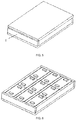
- the temporary jig comprises a first substrate 1 with a plurality of placement grooves 2, and a cover plate 3 detachably connected to the first substrate 1 and forming a box structure with a side opening with the first substrate 1, the plurality of placement grooves 2 being located in the box structure, and placement groove inlets 4 of each placement groove 2 communicating with the side openings. It is also possible to push the LEDs into the placement grooves 2 through the placement groove inlets 4 and position the LEDs through the placement grooves 2.
- the first substrate 1 comprises a first substrate 1 body, two first side plates which are arranged in parallel and two second side plates which are arranged perpendicular to the first side plates, the first side plates and the second side plates being arranged around the first substrate 1 body.
- a plurality of baffle plates are arranged on the first substrate 1 body along an extension direction of the first side plate, and the baffle plates and the first side plates form a plurality of placement grooves 2.
- the first side plate, the second side plate and the plurality of baffle plates are all equal in height.
- a width of the placement groove 2 is matched with a width of the LED to be placed, a groove depth of the placement groove 2 is matched with a thickness of the LED to be placed, and a length of the placement groove 2 can be determined according to a size of the LED display screen.
- the LED can thus be pushed into the placement groove 2 and can also be positioned by the placement groove 2.
- the two adjacent placement grooves 2 may be separated by a baffle plate having a thickness equal to spacing between adjacent LEDs.
- the baffle plate between two adjacent placement grooves 2 can be replaced, that is, the baffle plate is detachably connected with the first substrate 1, so that the baffle plate can be replaced according to the interval requirement of LED of each color of the LED display screen to be processed, and the universality of the jig is improved.
- the LEDs include R-color LEDs 5, G-color LEDs 6, and B-color LEDs 7.
- the three-color LEDs are alternately pushed into the placement grooves 2, at least one LED is placed in each placement groove 2, and the colors and the numbers of the LEDs placed in each placement groove 2 are the same.
- the plurality of placement grooves 2 can be ordered (for example, according to the placement order of the placement grooves 2).
- the R-color LEDs are sequentially pushed into the first ordered placement grooves 2.
- the G-color LEDs are sequentially pushed into the second ordered placement grooves 2, and when the second ordered placement grooves 2 are filled, B-color LEDs are sequentially pushed into the third ordered placement grooves 2.
- the process is repeated until all the placement grooves 2 are filled, so that the three-color LEDs of R, G and B (5, 6 and 7) can be uniformly arranged, and the color saturation of the LED display screen is improved.
- the number of LEDs of R, G and B colors of the LED display screen configuration is the same, that is, the number of the placement grooves 2 is a multiple of three.
- the color and the number of the LEDs placed in each of the placement grooves 2 and the arrangement of the three-color LEDs of R, G and B may be determined according to the placement relationship of the three-color LEDs of R, G and B in the LED display screen, which will not be described here.
- a light emitting surface of the LED faces towards the first substrate 1 body, so that the LED can be pushed into the placement groove 2 conveniently.
- a flatness of the light emitting surface of the LED is better than that of a welding pin surface, a friction force between the LED and the placement groove 2 can be reduced when the LED is pushed into the placement groove 2, and the LED can be pushed into the placement groove 2 conveniently.
- abrasion to the welding pin surfaces of the LEDs in the pushing-in process can be reduced, the probability of poor contact between welding and a circuit board 12 is reduced, and the quality of the LEDs is improved.
- the side cover 8 is used for covering the placement groove inlet 4 of the temporary jig.
- the temporary jig is closed into a closed box body, and the LED is positioned in the closed box body.
- the cover plate 3 covered on the first substrate 1 is removed, so that the welding pin surfaces of the LEDs are exposed.
- the cover plate 3 covers the first substrate 1, and the LED is located in the box body formed by the first substrate 1 and the cover plate 3, so that the welding leg surface of the LED faces the cover plate 3, and when the cover plate 3 is removed, the welding leg surface of the LED is exposed.
- attaching the temporary jig with a side cover, replacing the cover plate by an LED substrate, and attaching each LED to the LED substrate comprises:
- the LED substrate is provided with a conductive adhesive layer
- the LED substrate 9 is mounted on the first substrate 1
- the LED substrate 9 covers each LED and each LED is electrically connected with the LED substrate 9 through the conductive adhesive layer. That is, the bonding surface of the LED faces the LED substrate 9, and the bonding surface of the LED is in contact with the conductive adhesive layer.
- the LED substrate 9 is pressed so that each LED is attached to the LED substrate 9.
- the LED substrate 9 adopts a TFT substrate.
- the TFT substrate further comprises a metal wire layer 92 and a second substrate 91, and the conductive adhesive layer 93, the metal wire layer 92 and the second substrate 91 are sequentially stacked.
- the conductive adhesive layer 93 is in contact with the LEDs, and the LEDs are attached to the second substrate 91 through the conductive adhesive layer 93.
- the conductive adhesive layer 93 can adopt an ACF adhesive layer, AND metal conductive particles 931 are doped in the ACF adhesive layer.
- the welding pins 51 of the LED are embedded in the ACF adhesive layer, and the metal conductive particles 931 in the ACF adhesive layer are used as conduction to conduct with metal wires arranged on the second substrate 91.
- the second substrate 91 may have the metal wire layer 92 formed thereon by coating, developing, and etching.
- a size of the ACF adhesive layer is smaller than that of the second substrate 91, so that the ACF adhesive layer can be prevented from overflowing the second substrate 91 when the ACF adhesive layer is pressed.
- a screen sealing layer 10 formed by the sealing is arranged along a circumferential direction of the LED array formed by the LEDs so as to seal the circumferential direction of the LED array and prevent light rays generated by the LED array from leaking from the circumferential direction.
- sealant may be used in the screen sealing, i.e. the LED substrate 9 is coated with the sealant.
- replacing the first substrate by a transparent layer, removing the side cover, sealing the LED substrate, and connecting a circuit board with the LED substrate to manufacture the LED display screen comprises:
- the transparent layer 11 covers the light emitting surface of the LEDs, covers and fixes the LEDs through the transparent layer 11, and light generated by the LEDs can be irradiated through the transparent layer 11, wherein the transparent layer 11 can be made of transparent glass or a transparent film.
- the circuit board 12 is connected with the metal wire layer 92 of the LED substrate 9, and is connected with an external driver through the circuit board 12 to drive the display screen.
- the circuit board 12 may be a PCB board or an FPC (Flexible Printed Circuit) line.
- the application provides an LED display screen as shown in Fig. 14 , wherein the LED display screen is prepared by adopting the manufacturing method of an LED display screen.
- the LED display screen comprises an LED array and an LED substrate, wherein the LED array is pressed on the LED substrate.
- the LED basically comprises a conductive adhesive layer 93, a metal wire layer 92 and a second substrate 91, wherein the conductive adhesive layer 93, the metal wire layer 92 and the second substrate 91 are sequentially stacked.
- the conductive adhesive layer 93 is in contact with the LEDs, and the LEDs are attached to the second substrate 91 through the conductive adhesive layer 93.
- the conductive adhesive layer 93 can adopt an ACF adhesive layer, AND metal conductive particles 931 are doped in the ACF adhesive layer.
- the welding surface of the LED is attached to the second substrate basically through the ACF adhesive layer, the welding pins 51 of the LED are embedded in the ACF adhesive layer, and the metal conductive particles 931 in the ACF adhesive layer are used as conduction to conduct with metal wires arranged on the second substrate 91.
- the second substrate 91 may have the metal wire layer 92 formed thereon by coating, developing, and etching.
- the ACF adhesive layer can be prevented from overflowing the second substrate 91 when the ACF adhesive layer is pressed.
- the LED display screen further comprises a transparent layer 11 positioned on the light emitting surface of the LED array, and a screening sealing layer 10 arranged around the LED array, wherein the transparent layer 11 can be used for covering and fixing each LED, and light generated by each LED can be irradiated out through the transparent layer 11, wherein the transparent layer 11 can be made of transparent glass or a transparent film.
- the screen sealing layer 10 is used for fixing and sealing the circumferential direction of the LED array.
- the LED display screen further comprises a circuit board 12, wherein the circuit board 12 is connected with the metal wire layer 92 of the LED substrate and is connected with an external driver through the circuit board 12 to drive the display screen.
- the circuit board 12 may be a PCB board or an FPC line.
Landscapes
- Devices For Indicating Variable Information By Combining Individual Elements (AREA)
- Led Device Packages (AREA)
Abstract
Description
- The disclosure relates to the field of display screens, in particular to an LED display screen and a manufacturing method therefor.
- With the development of LED (Light Emitting Diode) display screen, the characteristics of MINI LED or MICRO LED display screen such as high brightness, high contrast, ultra-high resolution and color saturation have been paid with more attention. The MINI LED or MICRO LED display screen is composed of a plurality of LED (R, G, B) arrays, and each LED can be independently driven, so that the MINI LED or MICRO LED display screen also has the advantages of power saving, high reaction speed and the like. However, at present, in the manufacturing process of the MINI LED or MICRO LED display screen, the LEDs need to be clamped and placed on the PCB one by one, and the LED welding pins are accurately aligned with the PCB (Printed Circuit Board) welding pads, so that on one hand, the technology and the manufacturing precision of manufacturing personnel are required to be high, and on the other hand, when a large amount of LEDs are transferred, a large amount of time needs to be divided through manual bonding alignment, so that the production efficiency of the MINI LED or MICRO LED display screen is low.
- In view of the defects of the prior art, the disclosure aims to provide an LED display screen and a manufacturing method therefor, which can quickly realize LED transfer and accurately realize bonding alignment of LEDs.
- The technical solution adopted by the application is as follows:
- A manufacturing method of an LED display screen, comprising:
- presetting a temporary jig consisting of a first substrate with a plurality of placement grooves and a cover plate, and alternately placing three-color LEDs of R (Red), G (Green) and B (Blue) in the placement grooves through inlets of the placement grooves, wherein the colors of the LEDs in the same placement groove are the same;
- attaching the temporary jig with a side cover, replacing the cover plate by an LED substrate, and attaching each LED to the LED substrate at a same time;
- replacing the first substrate by a transparent layer, removing the side cover and sealing the LED substrate at a same time, and connecting a circuit board with the LED substrate to manufacture the LED display screen.
- As a further improved technical solution, attaching the temporary jig with a side cover, replacing the cover plate by an LED substrate, and attaching each LED to the LED substrate comprises:
- attaching the temporary jig with the side cover and removing the cover plate, wherein the side cover covers inlets of the placement grooves;
- pressing the LED substrate with a conductive adhesive layer on the first substrate, arranging the LED substrate on a side of LED away from the first substrate and electrically connecting the LED substrate with each LED through the conductive adhesive layer.
- As a further improved technical solution, replacing the first substrate by a transparent layer, removing the side cover and sealing the LED substrate at a same time, and connecting a circuit board with the LED substrate to manufacture the LED display screen comprises:
- removing the first substrate and the side cover, and coating the LED substrate with sealant along a circumferential direction to perform side screen sealing on the LED substrate;
- manufacturing the LED display screen by adopting a transparent layer to seal the LED substrate on upper side and connecting the circuit board with the LED substrate, wherein the transparent layer covers a light emitting surface of the LED.
- As a further improved technical solution, the transparent layer is one of a transparent glass or a thin film.
- As a further improved technical solution, the cover plate and the first substrate form a side opening box structure, and the plurality of placement grooves are located in the box structure and are all communicated with the side opening.
- As a further improved technical solution, the first substrate comprises a first substrate body, a plurality of first side plates arranged in parallel around the first substrate body, and a second side plate arranged perpendicular to the first side plate; a plurality of baffle plates are arranged on the first substrate body along an extension direction of the first side plate, and the baffle plates and the first side plates form a plurality of placement grooves.
- As a further improved technical solution, light emitting surfaces of the three-color LEDs of R, G and B are attached to the first substrate body.
- As a further improved technical solution, an amount of the plurality of placement grooves is a multiple of three.
- As a further improved technical solution, at least one LED is placed in the placement groove, and an amount of the LEDs placed in each placement groove is the same.
- As a further improved technical solution, the LED substrate further comprises a metal wire layer and a second substrate, the conductive adhesive layer, the metal wire layer and the second substrate are sequentially stacked, and each LED is fixed on the second substrate through the conductive adhesive layer and electrically connected with the metal wire layer.
- As a further improved technical solution, the conductive adhesive layer is an ACF (Anisotropic conductive film) adhesive layer, and metal conductive particles are arranged in the ACF adhesive layer to electrically connect an LED pin with a metal layer through the metal conductive particles.
- As a further improved technical solution, a size of the ACF adhesive layer is smaller than a size of the second substrate.
- As a further improved technical solution, the screen sealing layer for sealing the LED substrate is arranged along a circumference of the LED array formed by the LEDs so as to seal the circumference of the LED array.
- An LED display screen, wherein the LED display screen is manufactured by the manufacturing method of an LED display screen as described in one of the previous solutions.
- As a further improved technical solution, the LED display screen comprises an LED array and an LED substrate, wherein the LED array is laminated on the LED substrate, the LED basically comprising a conductive adhesive layer, a metal wire layer and a second substrate, the conductive adhesive layer, the metal wire layer and the second substrate being sequentially stacked, the conductive adhesive layer being in contact with each LED, and each LED being attached to the second substrate through the conductive adhesive layer.
- The LED is placed in the placement groove of the temporary jig, the cover plate of the temporary jig is replaced by the LED substrate, and the LED substrate is pressed with the LED, so that the LED is quickly connected with the LED substrate, and the production efficiency of the LED screen can be greatly improved.
- Embodiments of the present disclosure will now be further described with reference to the accompanying drawings, in which:
-
Fig. 1 is a flow diagram of one embodiment of a manufacturing method of an LED display screen provided by the present application. -
Fig. 2 is a schematic diagram showing the structure of a first substrate in the manufacturing method of an LED display screen provided by the present application. -
Fig. 3 is a schematic diagram showing the structure of a temporary jig in the manufacturing method of an LED display screen provided by the present application. -
Fig. 4 is a schematic diagram of a temporary jig equipped with LEDs in the manufacturing method of an LED display screen provided by the present application. -
Fig. 5 is a schematic diagram showing the structure of the LED display screen after a side cover is attached in the manufacturing method of an LED display screen provided by the present application. -
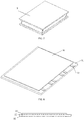
Fig. 6 is a schematic diagram of the LED display screen after a cover plate is removed in the manufacturing method of an LED display screen provided by the present application. -
Fig. 7 is a schematic diagram of the LED display screen after an LED substrate is attached in the manufacturing method of an LED display screen provided by the present application. -
Fig. 8 is a schematic diagram showing the structure in a view angle of an LED substrate in the manufacturing method of an LED display screen provided by the present application. -
Fig. 9 is a schematic diagram showing the structure in another view angle of the LED substrate in the manufacturing method of an LED display screen provided by the present application. -
Fig. 10 is a schematic diagram showing the structure in another view angle of the LED substrate in the manufacturing method of an LED display screen provided by the present application. -
Fig. 11 is a schematic diagram showing the structure of the LED display screen after the first substrate and the side plate are removed in the manufacturing method of an LED display screen provided by the present application. -
Fig. 12 is a schematic diagram of an LED display screen after a sealing layer is attached in the manufacturing method of an LED display screen provided by the present application. -
Fig. 13 is a schematic diagram of the LED display screen after a transparent layer is attached in the manufacturing method of an LED display screen provided by the present application. -
Fig. 14 is a schematic diagram showing the structure of an LED display screen provided by the present application. - The application provides an LED display screen and a manufacturing method therefor, in order to make the purpose, technical solution and effect of the application clearer and more definite, the application is described in further detail below. It should be understood that the embodiments described herein are merely illustrative of the present application and are not intended to be limiting therefor.
- The embodiment of the disclosure provides a manufacturing method of an LED display screen, which is illustrated in
fig. 1 and comprises the following steps: - S10, presetting a temporary jig consisting of a first substrate with a plurality of placement grooves and a cover plate, and alternately placing three-color LEDs of R, G and B in the placement grooves through inlets of the placement grooves, wherein the colors of the LEDs in the same placement groove are the same;
- S20, attaching the temporary jig with a side cover, replacing the cover plate by an LED substrate, and attaching each LED to the LED substrate;
- S30, replacing the first substrate by a transparent layer, removing the side cover, sealing the LED substrate, and connecting a circuit board with the LED substrate to manufacture the LED display screen.
- According to the disclosure, the three-color LEDs of R, G and B are sequentially placed into each placement groove of the temporary jig, the three-color LEDs of R, G and B are fixed through the temporary jig, and then the cover plate is replaced by the LED substrate which is laminated with the A plurality of three-color LEDs of R, G and B are simultaneously aligned with and laminated with the LED substrate, and the rapid transfer of the LED is realized, so that the production efficiency of the LED is improved.
- In the step S10, the temporary jig is a jig for manufacturing the LED display screen. As shown in
Figs. 2 and3 , the temporary jig comprises afirst substrate 1 with a plurality ofplacement grooves 2, and acover plate 3 detachably connected to thefirst substrate 1 and forming a box structure with a side opening with thefirst substrate 1, the plurality ofplacement grooves 2 being located in the box structure, andplacement groove inlets 4 of eachplacement groove 2 communicating with the side openings. It is also possible to push the LEDs into theplacement grooves 2 through theplacement groove inlets 4 and position the LEDs through theplacement grooves 2. In the embodiment, thefirst substrate 1 comprises afirst substrate 1 body, two first side plates which are arranged in parallel and two second side plates which are arranged perpendicular to the first side plates, the first side plates and the second side plates being arranged around thefirst substrate 1 body. A plurality of baffle plates are arranged on thefirst substrate 1 body along an extension direction of the first side plate, and the baffle plates and the first side plates form a plurality ofplacement grooves 2. The first side plate, the second side plate and the plurality of baffle plates are all equal in height. - A width of the
placement groove 2 is matched with a width of the LED to be placed, a groove depth of theplacement groove 2 is matched with a thickness of the LED to be placed, and a length of theplacement groove 2 can be determined according to a size of the LED display screen. The LED can thus be pushed into theplacement groove 2 and can also be positioned by theplacement groove 2. In this embodiment, the twoadjacent placement grooves 2 may be separated by a baffle plate having a thickness equal to spacing between adjacent LEDs. Of course, in practical applications, the baffle plate between twoadjacent placement grooves 2 can be replaced, that is, the baffle plate is detachably connected with thefirst substrate 1, so that the baffle plate can be replaced according to the interval requirement of LED of each color of the LED display screen to be processed, and the universality of the jig is improved. - Meanwhile, in the present embodiment, as shown in
Fig. 4 , the LEDs include R-color LEDs 5, G-color LEDs 6, and B-color LEDs 7. The three-color LEDs are alternately pushed into theplacement grooves 2, at least one LED is placed in eachplacement groove 2, and the colors and the numbers of the LEDs placed in eachplacement groove 2 are the same. In practical applications, the plurality ofplacement grooves 2 can be ordered (for example, according to the placement order of the placement grooves 2). The R-color LEDs are sequentially pushed into the first orderedplacement grooves 2. When the first orderedplacement grooves 2 are filled, the G-color LEDs are sequentially pushed into the second orderedplacement grooves 2, and when the second orderedplacement grooves 2 are filled, B-color LEDs are sequentially pushed into the third orderedplacement grooves 2. After the third orderedplacement grooves 2 are filled, the process is repeated until all theplacement grooves 2 are filled, so that the three-color LEDs of R, G and B (5, 6 and 7) can be uniformly arranged, and the color saturation of the LED display screen is improved. Further, in order to provide color saturation of the LED display screen, the number of LEDs of R, G and B colors of the LED display screen configuration is the same, that is, the number of theplacement grooves 2 is a multiple of three. Of course, in a modified embodiment of the present embodiment, the color and the number of the LEDs placed in each of theplacement grooves 2 and the arrangement of the three-color LEDs of R, G and B may be determined according to the placement relationship of the three-color LEDs of R, G and B in the LED display screen, which will not be described here. - Furthermore, when the LED is pushed into the
placement groove 2, a light emitting surface of the LED faces towards thefirst substrate 1 body, so that the LED can be pushed into theplacement groove 2 conveniently. A flatness of the light emitting surface of the LED is better than that of a welding pin surface, a friction force between the LED and theplacement groove 2 can be reduced when the LED is pushed into theplacement groove 2, and the LED can be pushed into theplacement groove 2 conveniently. Meanwhile, abrasion to the welding pin surfaces of the LEDs in the pushing-in process can be reduced, the probability of poor contact between welding and acircuit board 12 is reduced, and the quality of the LEDs is improved. - In the step S20, as shown in
Fig. 5 , theside cover 8 is used for covering theplacement groove inlet 4 of the temporary jig. When theside cover 8 is attached to the temporary jig, the temporary jig is closed into a closed box body, and the LED is positioned in the closed box body. In addition, as shown inFig. 6 , after theside cover 8 is attached to the temporary jig, thecover plate 3 covered on thefirst substrate 1 is removed, so that the welding pin surfaces of the LEDs are exposed. This is because the light emitting surface of the LED faces thefirst substrate 1 body, thecover plate 3 covers thefirst substrate 1, and the LED is located in the box body formed by thefirst substrate 1 and thecover plate 3, so that the welding leg surface of the LED faces thecover plate 3, and when thecover plate 3 is removed, the welding leg surface of the LED is exposed. - As an example, attaching the temporary jig with a side cover, replacing the cover plate by an LED substrate, and attaching each LED to the LED substrate comprises:
- S21, attaching the temporary jig with the side cover and removing the cover plate, wherein the side cover covers the inlet of the placement groove;
- S22, pressing an LED substrate provided with a conductive adhesive layer on the first substrate, wherein the LED substrate is positioned on one side, far away from the first substrate, of the LED and is electrically connected with each LED through the conductive adhesive layer.
- As shown in
Fig. 7 , the LED substrate is provided with a conductive adhesive layer, theLED substrate 9 is mounted on thefirst substrate 1, theLED substrate 9 covers each LED and each LED is electrically connected with theLED substrate 9 through the conductive adhesive layer. That is, the bonding surface of the LED faces theLED substrate 9, and the bonding surface of the LED is in contact with the conductive adhesive layer. In addition, when theLED substrate 9 is mounted on the first substrate, theLED substrate 9 is pressed so that each LED is attached to theLED substrate 9. - As shown in
Figs. 8-10 , theLED substrate 9 adopts a TFT substrate. the TFT substrate further comprises ametal wire layer 92 and asecond substrate 91, and the conductiveadhesive layer 93, themetal wire layer 92 and thesecond substrate 91 are sequentially stacked. The conductiveadhesive layer 93 is in contact with the LEDs, and the LEDs are attached to thesecond substrate 91 through the conductiveadhesive layer 93. The conductiveadhesive layer 93 can adopt an ACF adhesive layer, AND metalconductive particles 931 are doped in the ACF adhesive layer. When the welding surface of the LED is attached to thesecond substrate 91 through the ACF adhesive layer, the welding pins 51 of the LED are embedded in the ACF adhesive layer, and the metalconductive particles 931 in the ACF adhesive layer are used as conduction to conduct with metal wires arranged on thesecond substrate 91. Therein, thesecond substrate 91 may have themetal wire layer 92 formed thereon by coating, developing, and etching. In addition, since sealant overflowing phenomenon occurs to the ACF adhesive layer in the pressing process, a size of the ACF adhesive layer is smaller than that of thesecond substrate 91, so that the ACF adhesive layer can be prevented from overflowing thesecond substrate 91 when the ACF adhesive layer is pressed. - Further, in the step S30, as shown in
Fig. 11 , theside cover 8 and thefirst substrate 1 are removed, leaving the LED attached to the LED substrate and theLED substrate 9. In addition, in order to fix the LEDs on theLED substrate 9 and seal the LEDs, as shown inFig. 12 , ascreen sealing layer 10 formed by the sealing is arranged along a circumferential direction of the LED array formed by the LEDs so as to seal the circumferential direction of the LED array and prevent light rays generated by the LED array from leaking from the circumferential direction. In this embodiment, sealant may be used in the screen sealing, i.e. theLED substrate 9 is coated with the sealant. - As an example, replacing the first substrate by a transparent layer, removing the side cover, sealing the LED substrate, and connecting a circuit board with the LED substrate to manufacture the LED display screen comprises:
- S31, removing the first substrate and the side cover, and performing side screen sealing on the LED substrate in the circumferential direction;
- S32, manufacturing the LED display screen by adopting a transparent layer to seal the LED substrate on upper side and connecting the circuit board with the LED substrate, wherein the transparent layer covers a light emitting surface of the LED.
- As shown in
Fig. 13 , thetransparent layer 11 covers the light emitting surface of the LEDs, covers and fixes the LEDs through thetransparent layer 11, and light generated by the LEDs can be irradiated through thetransparent layer 11, wherein thetransparent layer 11 can be made of transparent glass or a transparent film. As shown inFig. 14 , thecircuit board 12 is connected with themetal wire layer 92 of theLED substrate 9, and is connected with an external driver through thecircuit board 12 to drive the display screen. Here, thecircuit board 12 may be a PCB board or an FPC (Flexible Printed Circuit) line. - The application provides an LED display screen as shown in
Fig. 14 , wherein the LED display screen is prepared by adopting the manufacturing method of an LED display screen. The LED display screen comprises an LED array and an LED substrate, wherein the LED array is pressed on the LED substrate. As shown inFigs. 9-11 , the LED basically comprises a conductiveadhesive layer 93, ametal wire layer 92 and asecond substrate 91, wherein the conductiveadhesive layer 93, themetal wire layer 92 and thesecond substrate 91 are sequentially stacked. The conductiveadhesive layer 93 is in contact with the LEDs, and the LEDs are attached to thesecond substrate 91 through the conductiveadhesive layer 93. The conductiveadhesive layer 93 can adopt an ACF adhesive layer, AND metalconductive particles 931 are doped in the ACF adhesive layer. When the welding surface of the LED is attached to the second substrate basically through the ACF adhesive layer, the welding pins 51 of the LED are embedded in the ACF adhesive layer, and the metalconductive particles 931 in the ACF adhesive layer are used as conduction to conduct with metal wires arranged on thesecond substrate 91. Therein, thesecond substrate 91 may have themetal wire layer 92 formed thereon by coating, developing, and etching. In addition, since the size of the ACF adhesive layer is smaller than that of the second substrate due to the sealant overflowing phenomenon of the ACF adhesive layer in the pressing process, the ACF adhesive layer can be prevented from overflowing thesecond substrate 91 when the ACF adhesive layer is pressed. - In addition, the LED display screen further comprises a
transparent layer 11 positioned on the light emitting surface of the LED array, and ascreening sealing layer 10 arranged around the LED array, wherein thetransparent layer 11 can be used for covering and fixing each LED, and light generated by each LED can be irradiated out through thetransparent layer 11, wherein thetransparent layer 11 can be made of transparent glass or a transparent film. Thescreen sealing layer 10 is used for fixing and sealing the circumferential direction of the LED array. In addition, the LED display screen further comprises acircuit board 12, wherein thecircuit board 12 is connected with themetal wire layer 92 of the LED substrate and is connected with an external driver through thecircuit board 12 to drive the display screen. Here, thecircuit board 12 may be a PCB board or an FPC line. - It is to be understood that the application of the present application is not limited to the examples described above, and that modifications or variations may be resorted to in light of the teachings by those of ordinary skill in the art, all falling within the scope of the appended claims.
Claims (15)
- A manufacturing method of an LED display screen, comprising:presetting a temporary jig consisting of a first substrate with a plurality of placement grooves and a cover plate, and alternately placing three-color LEDs of R, G and B in the placement grooves through inlets of the placement grooves, wherein the colors of the LEDs in the same placement groove are the same;attaching the temporary jig with a side cover, replacing the cover plate by an LED substrate and attaching each LED to the LED substrate at a same time;replacing the first substrate by a transparent layer, removing the side cover andsealing the LED substrate at a same time, and connecting a circuit board with the LED substrate to manufacture the LED display screen.
- The manufacturing method of an LED display screen according to claim 1, wherein attaching the temporary jig with a side cover, replacing the cover plate by an LED substrate, and attaching each LED to the LED substrate comprises:attaching the temporary jig with the side cover and removing the cover plate,wherein the side cover covers the inlet of the placement groove;pressing the LED substrate provided with a conductive adhesive layer on the first substrate, and electrically connecting the LED substrate with each LED through the conductive adhesive layer.
- The manufacturing method of an LED display screen according to claim 1, wherein replacing the first substrate by a transparent layer, removing the side cover and sealing the LED substrate at a same time, and connecting a circuit board with the LED substrate to manufacture the LED display screen comprises:removing the first substrate and the side cover, and coating the LED substrate with sealant along a circumferential direction to perform side screen sealing on the LED substrate;manufacturing the LED display screen by adopting a transparent layer to seal the LED substrate on upper side and connecting the circuit board with the LED substrate, wherein the transparent layer covers a light emitting surface of the LED.
- The manufacturing method of an LED display screen according to claim 3, wherein the transparent layer is one of a transparent glass or a thin film.
- The manufacturing method of an LED display screen according to claim 1, wherein the cover plate and the first substrate form a side opening box structure, and the plurality of placement grooves are located in the box structure and are all communicated with the side opening.
- The manufacturing method of an LED display screen according to claim 1, wherein the first substrate comprises a first substrate body, a plurality of first side plates arranged in parallel around the first substrate body, and a second side plate arranged perpendicular to the first side plate; a plurality of baffle plates are arranged on the first substrate body along an extension direction of the first side plate, and the baffle plates and the first side plates form a plurality of placement grooves.
- The manufacturing method of an LED display screen according to claim 6, wherein light emitting surfaces of the three-color LEDs of R, G and B are attached to the first substrate body.
- The manufacturing method of an LED display screen according to claim 1, wherein an amount of the plurality of placement grooves is a multiple of three.
- The manufacturing method of an LED display screen according to claim 1, wherein at least one LED is placed in the placement groove, and an amount of the LEDs placed in each placement groove is the same.
- The manufacturing method of an LED display screen according to claim 1, wherein the LED substrate further comprises a metal wire layer and a second substrate, the conductive adhesive layer, the metal wire layer and the second substrate are sequentially stacked, and each LED is fixed on the second substrate through the conductive adhesive layer and electrically connected with the metal wire layer.
- The manufacturing method of an LED display screen according to claim 10, wherein the conductive adhesive layer is an ACF adhesive layer, and metal conductive particles are arranged in the ACF adhesive layer to electrically connect an LED pin with a metal layer through the metal conductive particles.
- The manufacturing method of an LED display screen according to claim 11, wherein a size of the ACF adhesive layer is smaller than a size of the second substrate.
- The manufacturing method of an LED display screen according to claim 1, wherein the screen sealing layer for sealing the LED substrate is arranged along a circumference of the LED array formed by the LEDs so as to seal the circumference of the LED array.
- An LED display screen, wherein the LED display screen is manufactured by the manufacturing method of an LED display screen according to any one of claims 1-9.
- The LED display screen according to claim 14, comprising an LED array and an LED substrate, wherein the LED array is laminated on the LED substrate, the LED basically comprising a conductive adhesive layer, a metal wire layer and a second substrate, the conductive adhesive layer, the metal wire layer and the second substrate being sequentially stacked, the conductive adhesive layer being in contact with each LED, and each LED being attached to the second substrate through the conductive adhesive layer.
Applications Claiming Priority (2)
| Application Number | Priority Date | Filing Date | Title |
|---|---|---|---|
| CN201810827538.8A CN110767104B (en) | 2018-07-25 | 2018-07-25 | LED display screen and preparation method thereof |
| PCT/CN2019/097334 WO2020020176A1 (en) | 2018-07-25 | 2019-07-23 | Led display screen and manufacturing method therefor |
Publications (2)
| Publication Number | Publication Date |
|---|---|
| EP3828952A1 true EP3828952A1 (en) | 2021-06-02 |
| EP3828952A4 EP3828952A4 (en) | 2022-05-04 |
Family
ID=69180371
Family Applications (1)
| Application Number | Title | Priority Date | Filing Date |
|---|---|---|---|
| EP19841475.7A Pending EP3828952A4 (en) | 2018-07-25 | 2019-07-23 | LED DISPLAY SCREEN AND METHOD OF MANUFACTURING THEREOF |
Country Status (4)
| Country | Link |
|---|---|
| US (1) | US11769786B2 (en) |
| EP (1) | EP3828952A4 (en) |
| CN (1) | CN110767104B (en) |
| WO (1) | WO2020020176A1 (en) |
Families Citing this family (1)
| Publication number | Priority date | Publication date | Assignee | Title |
|---|---|---|---|---|
| CN116207204B (en) * | 2023-02-20 | 2025-09-16 | 惠科股份有限公司 | Backlight module, replacement method of light-emitting component in backlight module and display device |
Family Cites Families (22)
| Publication number | Priority date | Publication date | Assignee | Title |
|---|---|---|---|---|
| JPS61256773A (en) | 1985-05-10 | 1986-11-14 | Nec Corp | Led element aligning method |
| JP2000100562A (en) | 1998-09-22 | 2000-04-07 | Hokuriku Electric Ind Co Ltd | Organic EL device and manufacturing method thereof |
| JP2003086355A (en) | 2001-09-05 | 2003-03-20 | Kiko Kenji Kagi Kofun Yugenkoshi | Sealing structure of organic EL element, sealing method and sealing device |
| KR100759896B1 (en) | 2006-06-15 | 2007-09-18 | 삼성전자주식회사 | Backlight module equipped with at least one light emitting device and its manufacturing method |
| KR101020992B1 (en) * | 2009-03-02 | 2011-03-09 | 엘지이노텍 주식회사 | Light emitting module and light unit having same |
| KR101139722B1 (en) | 2010-03-17 | 2012-04-26 | 세크론 주식회사 | Jig for manufacturing LED module |
| CN101937926A (en) | 2010-09-08 | 2011-01-05 | 四川虹视显示技术有限公司 | Packaging structure of OLED display device |
| CN102610631B (en) | 2012-03-29 | 2015-06-17 | 信利半导体有限公司 | OLED (organic light-emitting diode) display device with adjustable surface color and preparation method of OLED display device |
| CN102931330A (en) * | 2012-11-12 | 2013-02-13 | 中国科学院半导体研究所 | Preparation method of LED (light-emitting diode) flat-panel display unit |
| CN103413897B (en) | 2013-08-07 | 2016-01-20 | 深圳市华星光电技术有限公司 | A kind of OLED encapsulating structure and method for packing |
| CN104576967A (en) | 2015-01-26 | 2015-04-29 | 深圳市华星光电技术有限公司 | OLED packaging structure and method |
| CN104576707B (en) * | 2015-01-28 | 2018-04-06 | 京东方科技集团股份有限公司 | O L ED panel, preparation method thereof and display device |
| KR102316325B1 (en) | 2015-07-06 | 2021-10-22 | 엘지전자 주식회사 | Display device using semiconductor light emitting device and method for manufacturing |
| CN105720179A (en) | 2016-02-04 | 2016-06-29 | 吴冬梅 | Anti-static LED display screen and manufacturing method thereof |
| CN105528969B (en) * | 2016-03-03 | 2019-03-15 | 京东方科技集团股份有限公司 | Display substrate, manufacturing method thereof, and display device |
| CN107768487A (en) * | 2016-08-18 | 2018-03-06 | 新世纪光电股份有限公司 | The method of flood tide transferred-electron device |
| CN106229421B (en) | 2016-08-24 | 2018-08-14 | 昆山工研院新型平板显示技术中心有限公司 | Flexible base board production method and flexible base board |
| CN106784382B (en) | 2016-12-30 | 2019-04-05 | 上海天马有机发光显示技术有限公司 | Packaging structure and packaging method of a display device |
| CN107731864B (en) * | 2017-11-20 | 2020-06-12 | 开发晶照明(厦门)有限公司 | Micro light emitting diode display and method of manufacture |
| CN108010994B (en) * | 2017-12-15 | 2019-10-18 | 惠州雷通光电器件有限公司 | micro light emitting diode transfer method |
| CN108258006B (en) * | 2017-12-21 | 2021-04-06 | 厦门市三安光电科技有限公司 | Micro light-emitting element |
| WO2021218478A1 (en) * | 2020-04-28 | 2021-11-04 | 海信视像科技股份有限公司 | Display apparatus |
-
2018
- 2018-07-25 CN CN201810827538.8A patent/CN110767104B/en active Active
-
2019
- 2019-07-23 WO PCT/CN2019/097334 patent/WO2020020176A1/en not_active Ceased
- 2019-07-23 EP EP19841475.7A patent/EP3828952A4/en active Pending
- 2019-07-23 US US17/257,449 patent/US11769786B2/en active Active
Also Published As
| Publication number | Publication date |
|---|---|
| US11769786B2 (en) | 2023-09-26 |
| CN110767104B (en) | 2021-09-28 |
| CN110767104A (en) | 2020-02-07 |
| WO2020020176A1 (en) | 2020-01-30 |
| EP3828952A4 (en) | 2022-05-04 |
| US20210225931A1 (en) | 2021-07-22 |
Similar Documents
| Publication | Publication Date | Title |
|---|---|---|
| TWI753715B (en) | Display apparatus | |
| CN110911391B (en) | Small pitch display module and manufacturing method thereof | |
| TWI682436B (en) | Massive transferring method of micro leds and light-emitting panel module using the method | |
| US11404472B2 (en) | Display module and display apparatus including light blocking layer with openings having regular intervals therebetween | |
| US20170077436A1 (en) | Display panel, display apparatus and method of manufacturing display panel | |
| WO2019082759A1 (en) | Inspection method for led chip, inspection device for same and method for manufacturing led display | |
| CN110880497B (en) | Small spacing display screen and production method thereof | |
| CN201946238U (en) | LED lattice display panel | |
| US7914194B2 (en) | Backlight unit having light emititng diodes and method of manufacturing the same | |
| JP4855845B2 (en) | Light emitting diode package manufacturing method, backlight unit, and liquid crystal display device | |
| WO2014190663A1 (en) | Backlight module and liquid crystal display device | |
| US11769786B2 (en) | LED display screen and manufacturing method therefor | |
| WO2022268109A1 (en) | Quantum dot complex, three-dimensional display element, and processing method for quantum dot complex | |
| KR102427474B1 (en) | LED Transfer device and transferring method using the same | |
| CN212725361U (en) | display components | |
| CN107283989B (en) | Pressing device and the method for pressing colloid on a display panel | |
| KR20200071497A (en) | A method for manufacturing the electronic device using microled | |
| KR20200009505A (en) | Display apparatus and manufacturing method thereof | |
| KR102378641B1 (en) | LED Light emitting unit and LED display device using the same | |
| US7741774B2 (en) | Backlight module including at least one luminescence element, and method of fabricating the same | |
| KR20230020034A (en) | PCB for mounting a mini LED and a backlight unit including the same | |
| US12593545B2 (en) | Display apparatus and manufacturing method thereof | |
| CN112701076A (en) | Display screen manufacturing method and system | |
| KR102046294B1 (en) | LED module and method of manufacturing the same and liquid crystal display device including LED module | |
| KR20250065991A (en) | Micro LED structure for display pixels, Display device including the same and micro LED repair process for display pixels |
Legal Events
| Date | Code | Title | Description |
|---|---|---|---|
| STAA | Information on the status of an ep patent application or granted ep patent |
Free format text: STATUS: THE INTERNATIONAL PUBLICATION HAS BEEN MADE |
|
| PUAI | Public reference made under article 153(3) epc to a published international application that has entered the european phase |
Free format text: ORIGINAL CODE: 0009012 |
|
| STAA | Information on the status of an ep patent application or granted ep patent |
Free format text: STATUS: REQUEST FOR EXAMINATION WAS MADE |
|
| 17P | Request for examination filed |
Effective date: 20201229 |
|
| AK | Designated contracting states |
Kind code of ref document: A1 Designated state(s): AL AT BE BG CH CY CZ DE DK EE ES FI FR GB GR HR HU IE IS IT LI LT LU LV MC MK MT NL NO PL PT RO RS SE SI SK SM TR |
|
| DAV | Request for validation of the european patent (deleted) | ||
| DAX | Request for extension of the european patent (deleted) | ||
| A4 | Supplementary search report drawn up and despatched |
Effective date: 20220404 |
|
| RIC1 | Information provided on ipc code assigned before grant |
Ipc: H01L 33/62 20100101ALN20220329BHEP Ipc: H01L 33/00 20100101ALI20220329BHEP Ipc: H01L 25/075 20060101AFI20220329BHEP |