EP3820143B1 - Bildgebungssystem und pixelmatrix und bildsensor dafür - Google Patents
Bildgebungssystem und pixelmatrix und bildsensor dafür Download PDFInfo
- Publication number
- EP3820143B1 EP3820143B1 EP19916831.1A EP19916831A EP3820143B1 EP 3820143 B1 EP3820143 B1 EP 3820143B1 EP 19916831 A EP19916831 A EP 19916831A EP 3820143 B1 EP3820143 B1 EP 3820143B1
- Authority
- EP
- European Patent Office
- Prior art keywords
- pixel
- pxa
- pxb
- signal
- reflected
- Prior art date
- Legal status (The legal status is an assumption and is not a legal conclusion. Google has not performed a legal analysis and makes no representation as to the accuracy of the status listed.)
- Active
Links
Images





Classifications
-
- G—PHYSICS
- G01—MEASURING; TESTING
- G01S—RADIO DIRECTION-FINDING; RADIO NAVIGATION; DETERMINING DISTANCE OR VELOCITY BY USE OF RADIO WAVES; LOCATING OR PRESENCE-DETECTING BY USE OF THE REFLECTION OR RERADIATION OF RADIO WAVES; ANALOGOUS ARRANGEMENTS USING OTHER WAVES
- G01S17/00—Systems using the reflection or reradiation of electromagnetic waves other than radio waves, e.g. lidar systems
- G01S17/88—Lidar systems specially adapted for specific applications
- G01S17/89—Lidar systems specially adapted for specific applications for mapping or imaging
- G01S17/894—Three-dimensional [3D] imaging with simultaneous measurement of time-of-flight at a two-dimensional [2D] array of receiver pixels, e.g. time-of-flight cameras or flash lidar
-
- H—ELECTRICITY
- H04—ELECTRIC COMMUNICATION TECHNIQUE
- H04N—PICTORIAL COMMUNICATION, e.g. TELEVISION
- H04N25/00—Circuitry of solid-state image sensors [SSIS]; Control thereof
- H04N25/70—SSIS architectures; Circuits associated therewith
-
- G—PHYSICS
- G01—MEASURING; TESTING
- G01S—RADIO DIRECTION-FINDING; RADIO NAVIGATION; DETERMINING DISTANCE OR VELOCITY BY USE OF RADIO WAVES; LOCATING OR PRESENCE-DETECTING BY USE OF THE REFLECTION OR RERADIATION OF RADIO WAVES; ANALOGOUS ARRANGEMENTS USING OTHER WAVES
- G01S7/00—Details of systems according to groups G01S13/00, G01S15/00, G01S17/00
- G01S7/48—Details of systems according to groups G01S13/00, G01S15/00, G01S17/00 of systems according to group G01S17/00
- G01S7/483—Details of pulse systems
- G01S7/486—Receivers
- G01S7/4861—Circuits for detection, sampling, integration or read-out
- G01S7/4863—Detector arrays, e.g. charge-transfer gates
-
- G—PHYSICS
- G01—MEASURING; TESTING
- G01S—RADIO DIRECTION-FINDING; RADIO NAVIGATION; DETERMINING DISTANCE OR VELOCITY BY USE OF RADIO WAVES; LOCATING OR PRESENCE-DETECTING BY USE OF THE REFLECTION OR RERADIATION OF RADIO WAVES; ANALOGOUS ARRANGEMENTS USING OTHER WAVES
- G01S7/00—Details of systems according to groups G01S13/00, G01S15/00, G01S17/00
- G01S7/48—Details of systems according to groups G01S13/00, G01S15/00, G01S17/00 of systems according to group G01S17/00
- G01S7/491—Details of non-pulse systems
- G01S7/4912—Receivers
- G01S7/4913—Circuits for detection, sampling, integration or read-out
- G01S7/4914—Circuits for detection, sampling, integration or read-out of detector arrays, e.g. charge-transfer gates
-
- G—PHYSICS
- G01—MEASURING; TESTING
- G01T—MEASUREMENT OF NUCLEAR OR X-RADIATION
- G01T1/00—Measuring X-radiation, gamma radiation, corpuscular radiation, or cosmic radiation
- G01T1/29—Measurement performed on radiation beams, e.g. position or section of the beam; Measurement of spatial distribution of radiation
- G01T1/2914—Measurement of spatial distribution of radiation
- G01T1/2964—Scanners
- G01T1/2971—Scanners using solid state detectors
-
- H—ELECTRICITY
- H04—ELECTRIC COMMUNICATION TECHNIQUE
- H04N—PICTORIAL COMMUNICATION, e.g. TELEVISION
- H04N25/00—Circuitry of solid-state image sensors [SSIS]; Control thereof
- H04N25/40—Extracting pixel data from image sensors by controlling scanning circuits, e.g. by modifying the number of pixels sampled or to be sampled
-
- H—ELECTRICITY
- H04—ELECTRIC COMMUNICATION TECHNIQUE
- H04N—PICTORIAL COMMUNICATION, e.g. TELEVISION
- H04N25/00—Circuitry of solid-state image sensors [SSIS]; Control thereof
- H04N25/70—SSIS architectures; Circuits associated therewith
- H04N25/76—Addressed sensors, e.g. MOS or CMOS sensors
- H04N25/77—Pixel circuitry, e.g. memories, A/D converters, pixel amplifiers, shared circuits or shared components
-
- H—ELECTRICITY
- H10—SEMICONDUCTOR DEVICES; ELECTRIC SOLID-STATE DEVICES NOT OTHERWISE PROVIDED FOR
- H10F—INORGANIC SEMICONDUCTOR DEVICES SENSITIVE TO INFRARED RADIATION, LIGHT, ELECTROMAGNETIC RADIATION OF SHORTER WAVELENGTH OR CORPUSCULAR RADIATION
- H10F39/00—Integrated devices, or assemblies of multiple devices, comprising at least one element covered by group H10F30/00, e.g. radiation detectors comprising photodiode arrays
- H10F39/10—Integrated devices
- H10F39/12—Image sensors
- H10F39/18—Complementary metal-oxide-semiconductor [CMOS] image sensors; Photodiode array image sensors
-
- H—ELECTRICITY
- H10—SEMICONDUCTOR DEVICES; ELECTRIC SOLID-STATE DEVICES NOT OTHERWISE PROVIDED FOR
- H10F—INORGANIC SEMICONDUCTOR DEVICES SENSITIVE TO INFRARED RADIATION, LIGHT, ELECTROMAGNETIC RADIATION OF SHORTER WAVELENGTH OR CORPUSCULAR RADIATION
- H10F39/00—Integrated devices, or assemblies of multiple devices, comprising at least one element covered by group H10F30/00, e.g. radiation detectors comprising photodiode arrays
- H10F39/10—Integrated devices
- H10F39/12—Image sensors
- H10F39/191—Photoconductor image sensors
- H10F39/194—Photoconductor image sensors having arrangements for blooming suppression
-
- H—ELECTRICITY
- H10—SEMICONDUCTOR DEVICES; ELECTRIC SOLID-STATE DEVICES NOT OTHERWISE PROVIDED FOR
- H10F—INORGANIC SEMICONDUCTOR DEVICES SENSITIVE TO INFRARED RADIATION, LIGHT, ELECTROMAGNETIC RADIATION OF SHORTER WAVELENGTH OR CORPUSCULAR RADIATION
- H10F39/00—Integrated devices, or assemblies of multiple devices, comprising at least one element covered by group H10F30/00, e.g. radiation detectors comprising photodiode arrays
- H10F39/80—Constructional details of image sensors
- H10F39/803—Pixels having integrated switching, control, storage or amplification elements
-
- G—PHYSICS
- G01—MEASURING; TESTING
- G01T—MEASUREMENT OF NUCLEAR OR X-RADIATION
- G01T1/00—Measuring X-radiation, gamma radiation, corpuscular radiation, or cosmic radiation
- G01T1/16—Measuring radiation intensity
- G01T1/20—Measuring radiation intensity with scintillation detectors
- G01T1/2018—Scintillation-photodiode combinations
-
- G—PHYSICS
- G01—MEASURING; TESTING
- G01T—MEASUREMENT OF NUCLEAR OR X-RADIATION
- G01T1/00—Measuring X-radiation, gamma radiation, corpuscular radiation, or cosmic radiation
- G01T1/29—Measurement performed on radiation beams, e.g. position or section of the beam; Measurement of spatial distribution of radiation
- G01T1/2914—Measurement of spatial distribution of radiation
- G01T1/2921—Static instruments for imaging the distribution of radioactivity in one or two dimensions; Radio-isotope cameras
- G01T1/2928—Static instruments for imaging the distribution of radioactivity in one or two dimensions; Radio-isotope cameras using solid state detectors
-
- H—ELECTRICITY
- H04—ELECTRIC COMMUNICATION TECHNIQUE
- H04N—PICTORIAL COMMUNICATION, e.g. TELEVISION
- H04N25/00—Circuitry of solid-state image sensors [SSIS]; Control thereof
- H04N25/70—SSIS architectures; Circuits associated therewith
- H04N25/76—Addressed sensors, e.g. MOS or CMOS sensors
- H04N25/78—Readout circuits for addressed sensors, e.g. output amplifiers or A/D converters
Definitions
- the present disclosure relates to imaging techniques and, more particularly, to a pixel array applicable to time-of-flight (ToF) imaging techniques, and a related image sensor and imaging system.
- ToF time-of-flight
- a time-of-flight (ToF) distance measuring technique calculates time of flight of the optical signal traveling from the transmitter side to the receiver side, thereby obtaining a distance between the target object and the transmitter/receiver side.
- the ToF distance measuring technique utilizes a planar light source with uniform illumination as an illumination source, such that each pixel in a pixel array can receive a light signal reflected from the distant target object.
- extremely high radiated power of the planar light source with uniform illumination not only increases system power consumption, but also causes damages to human eyes in face recognition applications.
- Document US2015/285625 A1 discloses sensing reflected light forming a plurality of reflected light spots and the document US2013/088621 A1 discloses an imaging system with photo diodes staggered in a second direction and arranged along a first direction in the context of focus pixels.
- Some embodiments of the present disclosure include an exemplary pixel array of an imaging system.
- the pixel array comprises a plurality of pixels arranged in rows and columns.
- the pixels are configured to sense a reflected signal, which is incident on the pixel array to form a plurality of reflected light spots separated from each other on the pixel array.
- Each of the pixels comprises a photodetector and a readout circuit.
- the photodetector is configured to detect the reflected signal and accordingly output a photo response signal.
- the readout circuit coupled to the photodetector, is configured to generate a pixel output according to the photo response signal.
- the pixels comprise a first pixel and a second pixel adjacent to the first pixel along a first predetermined direction.
- the readout circuit of the first pixel is adjacent to the photodetector of the second pixel along the first predetermined direction, and is adjacent to the photodetector of the first pixel along a second predetermined direction perpendicular to the first predetermined direction.
- Some embodiments of the present disclosure include an exemplary image sensor of an imaging system.
- the image sensor comprises a pixel array and a processing circuit.
- the pixel array is configured to sense a reflected signal, which is incident on the pixel array to form a plurality of reflected light spots separated from each other on the pixel array.
- the reflected signal is reflected from a target object in response to a structured light signal sent from the imaging system and reflected by the target object.
- the pixel array comprises a plurality of pixels arranged in rows and columns.
- Each of the pixels comprises a photodetector and a readout circuit.
- the photodetector is configured to detect the reflected signal and accordingly output a photo response signal.
- the readout circuit coupled to the photodetector, is configured to generate a pixel output according to the photo response signal.
- the pixels comprise a first pixel and a second pixel adjacent to the first pixel along a first predetermined direction.
- the readout circuit of the first pixel is adjacent to the photodetector of the second pixel along the first predetermined direction, and is adjacent to the photodetector of the first pixel along a second predetermined direction perpendicular to the first predetermined direction.
- the processing circuit coupled to the pixel array, is configured to detect time of flight of the structured light signal according to a sensing result of the pixel array, and obtain depth information about the target object according to the time of flight.
- the imaging system comprises a light emitting unit and a pixel array.
- the light emitting unit is configured to send a structured light signal.
- the pixel array is configured to sense a reflected signal, which is reflected from a target object in response to the structured light signal reflected by the target object.
- the pixel array comprises a plurality of pixels arranged in rows and columns.
- the reflected signal is incident on the pixel array to form a plurality of reflected light spots separated from each other on the pixel array.
- Each of the pixels comprises a photodetector and a readout circuit.
- the photodetector is configured to detect the reflected signal and accordingly output a photo response signal.
- the readout circuit coupled to the photodetector, is configured to generate a pixel output according to the photo response signal.
- the pixels comprise a first pixel and a second pixel adjacent to the first pixel along a first predetermined direction.
- the readout circuit of the first pixel is adjacent to the photodetector of the second pixel along the first predetermined direction, and is adjacent to the photodetector of the first pixel along a second predetermined direction perpendicular to the first predetermined direction.
- FIG. 1 is a block diagram illustrating an exemplary imaging system in accordance with an embodiment of the present disclosure.
- the imaging system 100 may be implemented using a three-dimensional (3D) imaging system, and configured to obtain depth information/image of a target object in the surroundings.
- the imaging system 100 may be a time-of-flight (ToF) imaging system, which can obtain depth information of a target object 102 by measuring a distance between the target object 102 and the imaging system 100.
- the imaging system 100 may be a structured light 3D imaging system, which may determine the depth information of the target object 102 according to distortion of a projected structured-light pattern received at a receiver side.
- the proposed imaging scheme is described below with reference to some embodiments where imaging system 100 is implemented as a ToF imaging system. However, those skilled in the art will recognize that the proposed imaging scheme can be applied to other 3D imaging systems which obtain depth images according to an optical signal sent from a transmitter side and received by a receiver side.
- the imaging system 100 may include, but is not limited to, a light emitting unit 110 and an image sensor 120.
- the light emitting unit 110 is configured to generate a structured light signal LS, wherein the structured light signal LS has a predetermined pattern such that energy of the structured light signal LS may be concentrated in the predetermined pattern.
- the light emitting unit 110 may include a light source 110 and an optical microstructure 114.
- the optical microstructure 114 can be arranged to change a travel path of an optical signal LI outputted from the light source 112, thereby generating the structured light signal LS having the predetermined pattern.
- projection of the structured light signal LS onto a cross section plane AB may form a plurality of light spots separated from each other. As a result, energy of the optical light LI can be concentrated in each light spot formed by the structured light signal LS, thereby increasing intensity of light incident on the target object 102 and reducing effects of background noise.
- the optical microstructure 114 may include a diffractive optical element (DOE) or a refractive optical element (ROE), and is configured to conically diffract or refract the optical signal LI to generate the structured light signal LS. Accordingly, the projection of the structured light signal LS onto the cross section plane AB may form a plurality of light spots separated from each other.
- DOE diffractive optical element
- ROE refractive optical element
- the image sensor 120 is configured to sense the reflected/reflection signal LR reflected from the target object 102 to thereby obtain image information of the target object 102.
- the reflected signal LR is generated in response to the structured light signal LR reflected by the target object 102.
- the image sensor 120 includes, but is not limited to, a pixel array 122 and a processing circuit 124.
- the pixel array 122 is configured to sense the reflected signal LR to generate a sensing result SR.
- the reflected signal LR incident on the pixel array 122 may form a plurality of reflected light spots/points separated from each other on the pixel array 122.
- the pixel array 122 includes a plurality of pixels, and each reflected light spot may illuminate at least one pixel.
- energy of the reflected signal LR can be concentrated and provided to pixels illuminated by the reflected light spots.
- a percentage of a background noise component in a light signal, received by a pixel illuminated by a reflected light spot may decrease to thereby enhance signal quality of a pixel output of the pixel (e.g. a portion of the sensing result SR).
- the processing circuit 124 coupled to the pixel array 122, is configured to detect time of flight of the structured light signal LS according to the sensing result SR of the pixel array 122, and obtain the depth information of the target object 102 according to the time of flight.
- the processing circuit 124 may refer to pixel output(s) generated from pixel(s) illuminated by the reflected light spots to obtain depth information (or a depth image) of an area illuminated by a plurality of light spots, which are formed on the surface of the target object 102 in response to the structured light signal LS.
- a distance between the light emitting unit 110 and each pixel in the pixel array 122 is much shorter than a distance between the light emitting unit 110 and the target object 102, and is much shorter than a distance between each pixel and the target object 102.
- time of flight of the structured light signal LS traveling from the light emitting unit 110 to the target object 102 may be regarded as equal to time of flight of the reflected signal LR traveling from the target object 102 to the pixel.
- the processing circuit 124 may therefore measure a distance between the target object 102 and the pixel according to the time of flight and a velocity of the structured light signal LS.
- the processing circuit 124 may determine depth information about an area of the surface of the target object 102, which is not illuminated by light spots of the structured light signal LS, according to depth information associated with pixels illuminated by the reflected light spots. The processing circuit 124 may therefore construct a depth image of the target object 102.
- the processing circuit 124 may generate refer to a pixel output of a pixel illuminated by the reflected light spots to perform related signal processing, such as interpolation, to thereby generate a pixel output of a pixel which is not illuminated by the reflected light spots.
- the pixel array 122 may utilize a small pixel pitch such that a reflected light spot can illuminate a sufficiently large area, such as at least one pixel, and enhance resolution.
- the imaging system 100 may not only reduce system power consumption by concentrating energy provided by a transmitter side, but also have good signal detection quality and high resolution.
- FIG. 2 and FIG. 3 illustrate distributions of light spots associated with the structured light signal LS and the reflected signal LR shown in FIG. 1 , respectively, in accordance with some embodiments of the present disclosure.
- Light spots shown in FIG. 2 and FIG. 3 are arranged in an array pattern having rows and columns.
- the structured light signal LS shown in FIG. 1 can be implemented by a structured light signal having a different distribution of light spots, e.g. light spots arranged in a polygon pattern and separated from each other, without departing from the scope of the present disclosure.
- the reflected signal LR shown in FIG. 1 can be implemented by a reflected signal having a different distribution of light spots, e.g. light spots arranged in a polygon pattern and separated from each other, without departing from the scope of the present disclosure.
- FIG. 2 a plurality of light spots formed by projection of the structured light signal LS onto the cross section plane AB shown in FIG. 1 is illustrated in FIG. 2 in accordance with an embodiment of the present disclosure.
- the optical microstructure 114 may be arranged to conically diffract the optical signal LI to generate the structured light signal LS, such that the projection of the structured light signal LS onto the cross section plane AB forms a plurality of light spots S1 arranged in M rows and N columns.
- M and N is a positive integer greater than one.
- the energy of the light signal LI, or the energy of the structured light signal LS can be concentrated in the light spots S1.
- a distance between two adjacent light spots shown in FIG. 2 is provided for illustrative purposes, and is not meant to be a limitation of the present disclosure.
- a distance between two adjacent light spots in a row direction and/or a distance between two adjacent light spots in a column direction can be adjusted by changing design of the optical microstructure 114.
- FIG. 3 a plurality of reflected light spots formed by the reflected signal LR incident on the pixel array 122 shown in FIG. 1 is illustrated in FIG. 3 in accordance with an embodiment of the present disclosure.
- the reflected signal LR can be reflected from the target object 102 in response to the structured light signal LS shown in FIG. 2 reflected by the target object 102.
- the reflected signal LR is incident on the pixel array 122 to form a plurality of reflected light spots S2 separated from each other on the pixel array 122.
- the pixel array 122 may include a plurality of pixels arranged in P rows and Q columns, where P is a positive integer greater than one and less than M, and Q is a positive integer greater than one and less than N.
- P is a positive integer greater than one and less than M
- Q is a positive integer greater than one and less than N.
- at least one pixel can be disposed between two adjacent reflected light spots of the reflected light spots S2.
- the pixel array 122 may have, but is not limited to, millions of pixels such as 1280 ⁇ 960 pixels.
- the light emitting unit 110 may use the structured light signal LS having 320 ⁇ 240 light sports, such that the reflected signal LR may form 320 ⁇ 240 reflected light sports on the pixel array 122.
- the pixel array 122 may use a smaller pixel pitch.
- a pixel array employed in the proposed imaging scheme may use an asymmetrical pixel array to meet requirements for small pixel pitches and high fill factors, and ensure that each reflected light spot can illuminate a photosensitive region of at least one pixel.
- a fill factor is a ratio of a photosensitive area to a total area of a pixel.
- each pixel of the pixel array 122 may include a photodetector and a readout circuit.
- the readout circuit of each pixel may be immediately adjacent to a photosensitive area of the pixel (e.g. the photodetector) in a row direction as well as in a column direction. Accordingly, each pixel may have a high fill factor.
- the pixels PXA and PXB are adjacent along a first predetermined direction D1 such as a column direction.
- the pixel PXA includes a photodetector PDA and a readout circuit RDA.
- the pixel PXB includes a photodetector PDB and a readout circuit RDB.
- the photodetector PDA is configured to detect the reflected signal LR and accordingly output a photo/light response signal DRA.
- the photodetector PDB is configured to detect the reflected signal LR and accordingly output a photo response signal DRB.
- the readout circuit RDA coupled to the photodetector PDA, is configured to generate a pixel output POA according to the photo response signal DRA.
- the readout circuit RDB coupled to the photodetector PDB, is configured to generate a pixel output POB according to the photo response signal DRB.
- the readout circuit RDA of the pixel PXA is adjacent to the photodetector PDB of the pixel PXB along the first predetermined direction D1, and is adjacent to the photodetector PDA of the pixel PXA along a second predetermined direction D2 (e.g. a column direction) perpendicular to first the predetermined direction D1.
- the photodetector PDA can be disposed at a side (e.g. an upper side) of the readout circuit RDA along the second predetermined direction D2, and the photodetector PDB can be disposed at another side (e.g. a lower side) of the readout circuit RDB opposite to the side along the second predetermined direction D2.
- the arrangement of the photodetector PDA and the readout circuit RDA in the pixel PXA and the arrangement of the photodetector PDB and the readout circuit RDB in the pixel PXB are inverted relative to each other.
- the pixel PXB may be regarded as an upside-down mirror image of the pixel PXA with respect to a pixel boundary BD.
- the readout circuit RDA/RDB may be immediately adjacent to a photosensitive area of a pixel in each of a row direction and a column direction.
- a length of each pixel along the second predetermined direction D2 may be longer than a length of the pixel along the first predetermined direction D1.
- a photosensitive area of each pixel (corresponding to a photosensitive region of a photodetector) may increase, thereby increasing a fill factor and sensitivity of the pixel.
- a length L of each pixel may be twice a width W of the pixel.
- the pixel array 122 may need only two readout circuits in a square-shaped area with side length L.
- the another pixel array would need four readout circuits which are located in four pixels respectively.
- the proposed imaging scheme may have a higher frame rate.
- first predetermined direction D1 and the second predetermined direction D2 are a row direction and a column direction respectively in the above paragraphs, this is not intended to limit the scope of the present disclosure.
- first predetermined direction D1 and the second predetermined direction D2 may be a column direction and a row direction respectively.
- the readout circuit of each pixel may include two photoelectric readout units, which are controlled by control signals having different phases.
- a processing circuit in a next stage can obtain information about a phase shift between a transmitted signal and a received signal, such as signal information used for continuous-wave (CW) modulation or pulsed modulation.
- CW continuous-wave
- the readout circuit RDA may include a first photoelectric readout unit 334 and a second photoelectric readout unit 336.
- the first photoelectric readout unit 334 is configured to be selectively coupled to the photodetector PDA according to a first control signal TX1, thereby generating a first portion of the pixel output POA of the pixel PXA.
- the second photoelectric readout unit 336 is configured to be selectively coupled to the photodetector PDA according to a second control signal TX2, thereby generating a second portion of the pixel output POA of the pixel PXA.
- the second control signal TX2 and the first control signal TX1 may have different phases.
- the readout circuit RDB may include a first photoelectric readout unit 344 and a second photoelectric readout unit 346.
- the first photoelectric readout unit 344 is configured to be selectively coupled to the photodetector PDB according to the first control signal TX1, thereby generating a first portion of the pixel output POB of the pixel PXB.
- the second photoelectric readout unit 346 is configured to be selectively coupled to the photodetector PDB according to the second control signal TX2, thereby generating a second portion of the pixel output POB of the pixel PXB.
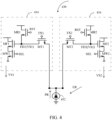
- FIG. 4 and FIG. 5 illustrate respective readout circuit structures of pixels applied to depth information measurements of a target object, which are obtained using CW modulation and pulsed modulation respectively, in accordance with some embodiments of the present disclosure.
- the circuit structures shown in FIG. 4 and FIG. 5 are not intended to limit the scope of the present disclosure.
- FIG. 4 a circuit structure of each pixel of the pixel array 122 shown in FIG. 3 used for a measurement scheme utilizing CW modulation is illustrated in accordance with some embodiments of the present disclosure.
- the pixel 430 may be used to implement the pixel PXA and the pixel PXB shown in FIG. 3 .
- the pixel 430 includes, but is not limited to, a photodetector 432, a first photoelectric readout unit 434 and a second photoelectric readout unit 436.
- the photodetector PDA/PDB shown in FIG. 3 can be implemented using the photodetector 432
- the first photoelectric readout unit 334/344 shown in FIG. 3 can be implemented using the first photoelectric readout unit 434
- the second photoelectric readout unit 336/346 shown in FIG. 3 can be implemented using the second photoelectric readout unit 436.
- the photodetector 432 such as a photodiode, can detect the reflected signal LR and accordingly generate a photo response signal PR.
- the photo response signal PR can be outputted through at least one of the first photoelectric readout unit 434 and the second photoelectric readout unit 436.
- the photodetector 432 may convert a received optical signal to a corresponding photocurrent signal.
- the photo response signal PR may be a current signal indicative of a signal level of an optical signal.
- a photoelectric readout unit can be configured to read the photocurrent signal.
- the first photoelectric readout unit 434 may include, but is not limited to, a first reset transistor MR1, a first transfer transistor MT1, a first output transistor MF1 and a first readout transistor MW1.
- the first reset transistor MR1 is configured to reset a first floating diffusion node FD1 according to a reset signal RST.
- the first transfer transistor MT1, coupled to the photodetector 432, is configured to be turned on according to the first control signal TX1. In other words, the first transfer transistor MT1 is controlled by the first control signal TX1, thereby being connected to or disconnected from the photodetector 432.
- the first output transistor MF1 is configured to amplify a voltage signal at the first floating diffusion node FD1, thereby generating a first amplified signal VS1.
- the first amplified signal VS1 can serve as a first portion of a pixel output of the pixel 430.
- the first readout transistor MW1 is configured to selectively output the first amplified signal VS1 according to a select signal SEL.
- the second photoelectric readout unit 436 is configured to be selectively coupled to the photodetector 432 according to a second control signal TX2, thereby generating a second portion of the pixel output of the pixel 430.
- the second control signal TX2 and the first control signal TX1 may have different phases.
- the second photoelectric readout unit 436 may include, but is not limited to, a second reset transistor MR2, a second transfer transistor MT2, a second output transistor MF2 and a second readout transistor MW2.
- the second reset transistor MR2 is configured to reset a second floating diffusion node FD2 according to the reset signal RST.
- the second transfer transistor MT2, coupled to the photodetector 432, is configured to be turned on according to the second control signal TX2.
- the second transfer transistor MT2 is controlled by the second control signal TX2, thereby being connected to or disconnected from the photodetector 432.
- the second output transistor MF2 is configured to amplify a voltage signal at the second floating diffusion node FD2, thereby generating a second amplified signal VS2.
- the second amplified signal VS2 can serve as a second portion of the pixel output of the pixel 430.
- the second readout transistor MW2 is configured to selectively output the second amplified signal VS2 according to a select signal SEL.
- first photoelectric readout unit 434 and the second photoelectric readout unit 436 which are configured to generate signal information used for CW modulation according to the first control signal TX1 and the second control signal TX2 respectively, further description is omitted here for brevity.
- FIG. 5 is a diagram illustrating a circuit structure of each pixel of the pixel array 122 shown in FIG. 3 used for a measurement scheme utilizing pulsed modulation in accordance with some embodiments of the present disclosure.
- the pixel 530 may be used to implement the pixel PXA and the pixel PXB shown in FIG. 3 .
- the difference between the circuit structure of the pixel 530 and the circuit structure of the pixel 430 shown in FIG. 4 is that the pixel 530 further includes an anti-blooming transistor MB.
- the anti-blooming transistor MB controlled by a third control signal TX3, is configured to extract photoelectrons, which are generated from the photodetector 432 in response to reception of ambient light, to enhance ambient light immunity of the pixel 530.
- first photoelectric readout unit 434 the second photoelectric readout unit 436 and the anti-blooming transistor MB, which are configured to generate signal information used for pulsed modulation according to the first control signal TX1, the second control signal TX2 and the third control signal TX3 respectively, further description is omitted here for brevity.
- each pixel of the pixel array 122 may be implemented using structures similar/identical to those of the pixel PXA and the pixel PXB. As a result, even if a center of a single reflected light spot S2 deviates from a photosensitive area of a single pixel, a photo response signal of sufficient intensity can be generated.
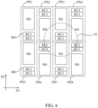
- the reflected light spot S2 shown in FIG. 3 is located at a boundary of two adjacent pixels shown in FIG. 6 in accordance with some embodiments of the present disclosure.
- the photodetector of each pixel i.e. each of the pixels PX1-PX8, is labeled PD for the sake of brevity.
- each readout circuit is labeled RD for the sake of brevity.
- Each readout circuit may include two photoelectric readout units RU1 and RU2, which can be implemented using the first photoelectric readout unit 334/344 and the second photoelectric readout unit 336/346 shown in FIG. 3 , respectively.
- the readout circuit RD of the pixel PX3 is adjacent to the respective photodetectors PD of the pixel PX2 and the pixel PX7 besides the respective photodetectors PD of the pixel PX3 and the pixel PX4.
- the pixel array 122 may provide a sufficient photosensitive area for detecting the reflected light spot S2 by arranging the respective photodetectors PD of a group of pixels disposed along the first predetermined D1 (e.g. a row of pixels) in a staggered manner in the second predetermined direction D2.
- FIG. 7 is a diagram illustrating the reflected light spot S2 shown in FIG. 3 located at a boundary of two adjacent pixels in accordance with some embodiments of the present disclosure.
- Each pixel of the pixel array shown in FIG. 3 may be implemented using the pixel architecture shown in FIG. 7 .
- the difference between the pixel arrangement shown in FIG. 7 and the pixel arrangement shown in FIG. 6 is that the photodetector PD of each pixel shown in FIG. 7 is disposed at a same side (e.g. an upper side) of the readout circuit RD of the pixel in the predetermined direction D2.
- the pixel PX2/PX4/PX6/PX8 may be implemented using an upside-down pixel relative to the pixel PXB shown in FIG. 3 .
- a group of pixels disposed along the first predetermined D1 may be arranged in a staggered manner in the second predetermined direction D2, such that a readout circuit of a single pixel may be enclosed by four photodetectors.
- the pixel array 122 may provide a sufficient photosensitive area for detecting the reflected light spot S2.
- FIG. 8 is a diagram illustrating the reflected light spot S2 shown in FIG. 3 located at a boundary of two adjacent pixels in accordance with some embodiments of the present disclosure.
- Each pixel of the pixel array shown in FIG. 3 may be implemented using the pixel architecture shown in FIG. 8 .
- the difference between the pixel arrangement shown in FIG. 8 and the pixel arrangement shown in FIG. 6 is that a photosensitive area of the photodetector PD of each pixel shown in FIG. 8 is non-quadrilateral in shape.
- the photodetector PD of each pixel has an L-shaped photosensitive area, and the corresponding readout circuit RD may be disposed at an inside corner of the L-shaped photosensitive area.
- the periphery of the readout circuit RD can be enclosed by photosensitive areas.
- the readout circuit RD of the pixel PX3 is adjacent to the photodetector PD of the pixel PX4 along the first predetermined direction D1, and is adjacent to the photodetector PD of the pixel PX3 along the second predetermined direction D2.
- the readout circuit RD of the pixel PX3 is adjacent to the photodetector PD of the pixel PX3 along a third predetermined direction D3 opposite to the first predetermined direction D1.
- FIG. 9 is a diagram illustrating the reflected light spot S2 shown in FIG. 3 located at a boundary of two adjacent pixels in accordance with some embodiments of the present disclosure.
- Each pixel of the pixel array shown in FIG. 3 may be implemented using the pixel architecture shown in FIG. 9 .
- a readout circuit located at a pixel boundary e.g. the second photoelectric readout unit RU2 of the pixel PX3 and the first photoelectric readout unit RU1 of the pixel PX7 can be enclosed by sufficient photosensitive areas.
- the pixel array 122 may provide a sufficient photosensitive area for detecting the reflected light spot S2.
- FIG. 10 is a diagram illustrating the reflected light spot S2 shown in FIG. 3 located at a boundary of two adjacent pixels in accordance with some embodiments of the present disclosure.
- Each pixel of the pixel array shown in FIG. 3 may be implemented using the pixel architecture shown in FIG. 10 .
- the difference between the pixel arrangement shown in FIG. 10 and the pixel arrangement shown in FIG. 6 is that a photosensitive area of the photodetector PD of each pixel shown in FIG. 10 is non-quadrilateral in shape.
- the first photoelectric readout unit RU1 and the second photoelectric readout unit RU2 of each pixel can be disposed at different sides of the photodetector PD.
- the photodetector PD of each pixel has a T-shaped photosensitive area.
- the corresponding first photoelectric readout unit RU1 may be disposed at an inside corner of the T-shaped photosensitive area, and the corresponding second photoelectric readout unit RU2 may be disposed at another inside corner of the T-shaped photosensitive area.
- a readout circuit located at a pixel boundary e.g. the second photoelectric readout unit RU2 of the pixel PX3 and the first photoelectric readout unit RU1 of the pixel PX7
- the pixel array 122 may provide a sufficient photosensitive area for detecting the reflected light spot S2.
- the proposed imaging scheme can make a reflected signal, reflected from a target object and returns to a receiver side, form a plurality of reflected light sports on a pixel array, thereby increasing signal intensity of an optical signal incident on pixels and reducing effects of background noise.
- the proposed imaging scheme may use an asymmetrical pixel arrangement, such as a pixel arrangement where each pixel is rectangular in shape, respective photosensitive areas of consecutive pixels are arranged in a staggered manner, and/or a photosensitive area is non-quadrilateral in shape. With the use of the asymmetrical pixel arrangement, the proposed imaging scheme may meet requirements for small pixel pitches and high fill factors, and have high sensitivity, high resolution and high frame rates.
Landscapes
- Engineering & Computer Science (AREA)
- Physics & Mathematics (AREA)
- General Physics & Mathematics (AREA)
- Multimedia (AREA)
- Signal Processing (AREA)
- Remote Sensing (AREA)
- Radar, Positioning & Navigation (AREA)
- Computer Networks & Wireless Communication (AREA)
- Electromagnetism (AREA)
- Health & Medical Sciences (AREA)
- Life Sciences & Earth Sciences (AREA)
- High Energy & Nuclear Physics (AREA)
- Molecular Biology (AREA)
- Spectroscopy & Molecular Physics (AREA)
- Solid State Image Pick-Up Elements (AREA)
- Optical Radar Systems And Details Thereof (AREA)
Claims (11)
- Ein Bildgebungssystem (100), bestehend aus:
einer Pixelmatrix (122), wobei ein reflektiertes Signal (LR) auf die Pixelmatrix (122) auftrifft, um eine Vielzahl von reflektierten Lichtpunkten (S2) zu bilden, die auf der Pixelmatrix (122) voneinander getrennt sind; die Pixelmatrix (122) umfasst:
mehrere in Zeilen und Spalten angeordnete Pixel (430, 530, PXA, PXB, PX1-PX8), wobei die Pixel (430, 530, PXA, PXB, PX1-PX8) so konfiguriert sind, dass sie das reflektierte Signal (LR) erfassen, und die Pixelmatrix (122) dadurch gekennzeichnet ist, dass jedes der Pixel (430, 530, PXA, PXB, PX1-PX8) Folgendes umfasst:einen Fotodetektor (432, PDA, PDB, PD), der so konfiguriert ist, dass er das reflektierte Signal (LR) erkennt und dementsprechend ein Fotoantwortsignal (DRA, DRB) ausgibt; undeine Ausleseschaltung (RDA, RDB, RD), die mit dem Fotodetektor (432, PDA, PDB, PD) gekoppelt ist, wobei die Ausleseschaltung (RDA, RDB, RD) so konfiguriert ist, dass sie eine Pixelausgabe (POA, POB, PO) entsprechend dem Fotoantwortsignal (DRA, DRB) erzeugt;wobei die jeweiligen Fotodetektoren (432, PDA, PDB, PD) einer Pixelgruppe der Pixel (430, 530, PXA, PXB, PX1-PX8) - die entlang einer ersten vorgegebenen Richtung (D1), entweder in Zeilen- oder in Spaltenrichtung angeordnet sind - versetzt in einer zweiten vorgegebenen Richtung (D2) und senkrecht zur ersten vorgegebenen Richtung (D1) angeordnet sind; die Pixelgruppe (430, 530, PXA, PXB, PX1-PX8) umfasst ein erstes Pixel (430, 530, PXA, PXB, PX1-PX8) und ein zweites Pixel (430, 530, PXA, PXB, PX1-PX8) neben dem ersten Pixel (430, 530, PXA, PXB, PX1-PX8) in der ersten vorgegebenen Richtung (D1); die Ausleseschaltung (RDA, RDB, RD) des ersten Pixels (430, 530, PXA, PXB, PX1-PX8) grenzt an den Fotodetektor (432, PDA, PDB, PD) des zweiten Pixels (430, 530, PXA, PXB, PX1-PX8) entlang der ersten vorgegebenen Richtung (D1) und ist neben dem Fotodetektor (432, PDA, PDB, PD) des ersten Pixels (430, 530, PXA, PXB, PX1-PX8) entlang der zweiten vorgegebenen Richtung (D2);wobei der Fotodetektor (432, PDA, PDB, PD) des ersten Pixels (430, 530, PXA, PXB, PX1-PX8) an einer ersten Seite der Ausleseschaltung (RDA, RDB, RD) des ersten Pixels (430, 530, PXA, PXB, PX1-PX8) entlang der zweiten vorgegebenen Richtung (D2) angeordnet ist; der Fotodetektor (432, PDA, PDB, PD) des zweiten Pixels (430, 530, PXA, PXB, PX1-PX8) ist unmittelbar neben der Ausleseschaltung des zweiten Pixels und an einer zweiten Seite der Ausleseschaltung (RDA, RDB, RD) des zweiten Pixels (430, 530, PXA, PXB, PX1-PX8) gegenüber der ersten Seite entlang der zweiten vorgegebenen Richtung (D2) angeordnet. - Bildgebungssystem (100) nach Anspruch 1, dadurch gekennzeichnet, dass eine Länge jedes Pixels (430, 530, PXA, PXB, PX1-PX8) in der ersten vorgegebenen Richtung (D1) kürzer ist als ein Abstand zwischen zwei benachbarten reflektierten Lichtpunkten der reflektierten Lichtpunkte (S2) in der ersten vorgegebenen Richtung (D1).
- Bildgebungssystem (100) nach einem der Ansprüche 1 und 2, dadurch gekennzeichnet, dass eine Länge jedes Pixels (430, 530, PXA, PXB, PX1-PX8) entlang der zweiten vorgegebenen Richtung (D2) länger ist als eine Länge des Pixels entlang der ersten vorgegebenen Richtung (D1).
- Bildgebungssystem (100) nach einem der Ansprüche 1-3, dadurch gekennzeichnet, dass die Ausleseschaltung (RDA, RDB, RD) des ersten Pixels (430, 530, PXA, PXB, PX1-PX8) Folgendes umfasst:eine erste fotoelektrische Ausleseeinheit (334, 344, 434, RUI), die so konfiguriert ist, dass sie gemäß einem ersten Steuersignal (TX1) selektiv mit dem Fotodetektor (432, PDA, PDB, PD) des ersten Pixels (430, 530, PXA, PXB, PX1-PX8) gekoppelt wird und einen ersten Teil der Pixelausgabe (POA, POB, PO) des ersten Pixels (430, 530, PXA, PXB, PX1-PX8) erzeugt; undeine zweite fotoelektrische Ausleseeinheit (336, 346, 436, RU2), die so konfiguriert ist, dass sie gemäß einem zweiten Steuersignal (TX2) selektiv mit dem Fotodetektor (432, PDA, PDB, PD) des ersten Pixels (430, 530, PXA, PXB, PX1-PX8) gekoppelt wird und einen zweiten Teil der Pixelausgabe (POA, POB, PO) des ersten Pixels (430, 530, PXA, PXB, PX1-PX8) erzeugt, wobei das zweite Steuersignal (TX2) und das erste Steuersignal (TX1) unterschiedliche Phasen aufweisen.
- Bildgebungssystem (100) nach Anspruch 4, dadurch gekennzeichnet, dass die erste fotoelektrische Ausleseeinheit (334, 344, 434, RU1) und die zweite fotoelektrische Ausleseeinheit (336, 346, 436, RU2) auf derselben Seite des Fotodetektors (432, PDA, PDB, PD) des ersten Pixels (430, 530, PXA, PXB, PX1-PX8) angeordnet sind.
- Bildgebungssystem (100) nach Anspruch 4, dadurch gekennzeichnet, dass die erste fotoelektrische Ausleseeinheit (434, RU1) und die zweite fotoelektrische Ausleseeinheit (436, RU2) jeweils auf gegenüberliegenden Seiten des Fotodetektors (432, PDA, PDB, PD) des ersten Pixels (430, 530, PX1-PX8) angeordnet sind.
- Bildgebungssystem (100) nach einem der Ansprüche 1-6, wobei das reflektierte Signal (LR) von einem Zielobjekt (102) als Reaktion auf ein strukturiertes Lichtsignal (LS) reflektiert wird, das vom Bildgebungssystem (100) gesendet und vom Zielobjekt (102) reflektiert wird; das Bildgebungssystem (100) umfasst ferner:
eine Verarbeitungsschaltung (124), die mit der Pixelmatrix (122) gekoppelt ist, wobei die Verarbeitungsschaltung (124) so konfiguriert ist, dass sie die Laufzeit des strukturierten Lichtsignals (LS) gemäß einem Abtastergebnis (SR) der Pixelmatrix (122) erfasst und Tiefeninformationen über das Zielobjekt (102) gemäß der Laufzeit erhält. - Bildgebungssystem (100) nach einem der Ansprüche 1-6, wobei das reflektierte Signal (LR) von einem Zielobjekt (102) als Reaktion auf ein strukturiertes Lichtsignal (LS) vom Zielobjekt (102) reflektiert wird; das Bildgebungssystem (100) umfasst ferner:
eine Licht emittierende Einheit (110), die so konfiguriert ist, dass sie das strukturierte Lichtsignal (LS) sendet. - Bildgebungssystem (100) nach Anspruch 8, dadurch gekennzeichnet, dass die Projektion des strukturierten Lichtsignals (LS) auf eine Querschnittsebene (AB) zwischen der Licht emittierenden Einheit (110) und dem Zielobjekt (102) eine Vielzahl voneinander getrennter Lichtpunkte (SI) bildet.
- Bildgebungssystem (100) nach Anspruch 8, dadurch gekennzeichnet, dass das reflektierte Signal (LR) auf die Pixelmatrix (122) auftrifft, um eine Vielzahl von reflektierten Lichtpunkten (S2) zu bilden, die auf der Pixelmatrix (122) voneinander getrennt sind, und jeder reflektierte Lichtpunkt (S2) mindestens ein Pixel (430, 530, PXA, PXB, PX1-PX8) beleuchtet.
- Bildgebungssystem (100) nach Anspruch 8, dadurch gekennzeichnet, dass die Licht emittierende Einheit (110) Folgendes umfasst:
eine Lichtquelle (112), die so angeordnet ist, dass sie ein optisches Signal (LI) ausgibt; und
eine optische Mikrostruktur (114), die so angeordnet ist, dass sie den Laufweg des optischen Signals (LI) ändert, um das strukturierte Lichtsignal (LS) zu erzeugen.
Applications Claiming Priority (1)
| Application Number | Priority Date | Filing Date | Title |
|---|---|---|---|
| PCT/CN2019/076295 WO2020172812A1 (zh) | 2019-02-27 | 2019-02-27 | 成像系统及成像系统的像素阵列和图像传感器 |
Publications (3)
| Publication Number | Publication Date |
|---|---|
| EP3820143A1 EP3820143A1 (de) | 2021-05-12 |
| EP3820143A4 EP3820143A4 (de) | 2021-05-12 |
| EP3820143B1 true EP3820143B1 (de) | 2024-08-21 |
Family
ID=67194571
Family Applications (1)
| Application Number | Title | Priority Date | Filing Date |
|---|---|---|---|
| EP19916831.1A Active EP3820143B1 (de) | 2019-02-27 | 2019-02-27 | Bildgebungssystem und pixelmatrix und bildsensor dafür |
Country Status (4)
| Country | Link |
|---|---|
| US (1) | US11442170B2 (de) |
| EP (1) | EP3820143B1 (de) |
| CN (1) | CN110024374B (de) |
| WO (1) | WO2020172812A1 (de) |
Families Citing this family (11)
| Publication number | Priority date | Publication date | Assignee | Title |
|---|---|---|---|---|
| EP3820143B1 (de) | 2019-02-27 | 2024-08-21 | Shenzhen Goodix Technology Co., Ltd. | Bildgebungssystem und pixelmatrix und bildsensor dafür |
| CN113037989B (zh) * | 2019-12-09 | 2022-11-18 | 华为技术有限公司 | 一种图像传感器、相机模组及控制方法 |
| CN114829970A (zh) * | 2019-12-23 | 2022-07-29 | 索尼半导体解决方案公司 | 飞行时间成像电路、飞行时间成像系统和飞行时间成像方法 |
| US11853142B2 (en) * | 2020-05-28 | 2023-12-26 | Apple Inc. | Sensor-based user detection for electronic devices |
| CN113038041B (zh) * | 2020-06-12 | 2022-09-13 | 深圳市汇顶科技股份有限公司 | 成像系统以及相关电子装置及成像系统的操作方法 |
| WO2021248427A1 (zh) | 2020-06-12 | 2021-12-16 | 深圳市汇顶科技股份有限公司 | 深度传感装置以及相关电子装置及深度传感装置的操作方法 |
| EP4020006B1 (de) * | 2020-12-23 | 2025-07-02 | STMicroelectronics (Research & Development) Limited | Time-of-flight sensor |
| CN112859046B (zh) * | 2021-01-19 | 2024-01-12 | Oppo广东移动通信有限公司 | 光接收模组、飞行时间装置及电子设备 |
| KR20230001394A (ko) * | 2021-06-28 | 2023-01-04 | 삼성전자주식회사 | 거리 측정을 위한 이미지 센서 및 이를 포함하는 이미지 센서 모듈 |
| CN117916621A (zh) * | 2021-10-08 | 2024-04-19 | 华为技术有限公司 | 一种探测系统、终端设备、控制探测方法及控制装置 |
| JP2024023058A (ja) * | 2022-08-08 | 2024-02-21 | ソニーセミコンダクタソリューションズ株式会社 | 光検出装置および光検出システム |
Family Cites Families (20)
| Publication number | Priority date | Publication date | Assignee | Title |
|---|---|---|---|---|
| EP2133918B1 (de) * | 2008-06-09 | 2015-01-28 | Sony Corporation | Festkörperabbildungsvorrichtung, entsprechendes Steuerungsverfahren und elektronische Vorrichtung |
| CN102157529A (zh) * | 2010-02-12 | 2011-08-17 | 联咏科技股份有限公司 | 影像传感器 |
| CN103826538B (zh) * | 2011-09-27 | 2016-06-22 | 富士胶片株式会社 | 放射线成像系统及其操作方法,以及放射线图像检测装置 |
| KR20130038035A (ko) * | 2011-10-07 | 2013-04-17 | 삼성전자주식회사 | 촬상소자 |
| US9541386B2 (en) * | 2012-03-21 | 2017-01-10 | Semiconductor Energy Laboratory Co., Ltd. | Distance measurement device and distance measurement system |
| EP2738812B8 (de) * | 2012-11-29 | 2018-07-18 | ams Sensors Belgium BVBA | Pixelanordnung |
| KR102003496B1 (ko) * | 2013-03-06 | 2019-10-01 | 삼성전자주식회사 | 이미지 센서 및 이미지 픽업 장치 |
| CN103561218B (zh) * | 2013-10-30 | 2019-07-19 | 上海集成电路研发中心有限公司 | 一种高光灵敏度cmos图像传感器像素结构 |
| KR102163728B1 (ko) * | 2013-12-05 | 2020-10-08 | 삼성전자주식회사 | 거리영상 측정용 카메라 및 이를 이용한 거리영상 측정방법 |
| CN104800054B (zh) * | 2014-01-27 | 2017-01-25 | 光宝电子(广州)有限公司 | 距离侦测与指示方法及具有此侦测与指示功能的行动装置 |
| US9952323B2 (en) * | 2014-04-07 | 2018-04-24 | Samsung Electronics Co., Ltd. | High resolution, high frame rate, low power image sensor |
| EP3188471A4 (de) * | 2014-08-29 | 2017-08-23 | Panasonic Intellectual Property Management Co., Ltd. | Bildgebungsvorrichtung |
| WO2016167044A1 (ja) * | 2015-04-14 | 2016-10-20 | ソニー株式会社 | 固体撮像装置、撮像システムおよび距離計測方法 |
| JPWO2017056347A1 (ja) * | 2015-09-29 | 2018-08-02 | パナソニック・タワージャズセミコンダクター株式会社 | 固体撮像装置 |
| CN108370424B (zh) * | 2015-12-16 | 2021-06-15 | 索尼公司 | 成像元件、驱动方法和电子设备 |
| JP6821967B2 (ja) * | 2016-06-24 | 2021-01-27 | 株式会社ニコン | 撮像装置 |
| CN106897688B (zh) * | 2017-02-21 | 2020-12-08 | 杭州易现先进科技有限公司 | 交互式投影装置、控制交互式投影的方法和可读存储介质 |
| CN208548353U (zh) * | 2018-08-22 | 2019-02-26 | 苏州多感科技有限公司 | 一种图像传感器和电子设备 |
| CN110313018A (zh) | 2018-09-18 | 2019-10-08 | 深圳市汇顶科技股份有限公司 | 深度信息建构系统、相关电子装置以及用以建构深度信息的方法 |
| EP3820143B1 (de) | 2019-02-27 | 2024-08-21 | Shenzhen Goodix Technology Co., Ltd. | Bildgebungssystem und pixelmatrix und bildsensor dafür |
-
2019
- 2019-02-27 EP EP19916831.1A patent/EP3820143B1/de active Active
- 2019-02-27 CN CN201980000288.3A patent/CN110024374B/zh active Active
- 2019-02-27 WO PCT/CN2019/076295 patent/WO2020172812A1/zh not_active Ceased
-
2020
- 2020-09-26 US US17/033,767 patent/US11442170B2/en active Active
Also Published As
| Publication number | Publication date |
|---|---|
| EP3820143A1 (de) | 2021-05-12 |
| CN110024374A (zh) | 2019-07-16 |
| CN110024374B (zh) | 2021-08-10 |
| WO2020172812A1 (zh) | 2020-09-03 |
| US20210011169A1 (en) | 2021-01-14 |
| EP3820143A4 (de) | 2021-05-12 |
| US11442170B2 (en) | 2022-09-13 |
Similar Documents
| Publication | Publication Date | Title |
|---|---|---|
| US11442170B2 (en) | Imaging system, pixel array of imaging system and image sensor | |
| JP6899005B2 (ja) | 光検出測距センサ | |
| US20220050201A1 (en) | Fmcw imaging lidar based on coherent pixel array | |
| US20200103507A1 (en) | Lidar 2d receiver array architecture | |
| US9048609B2 (en) | Laser emitter module and laser detecting system to which the laser emitter module is applied | |
| KR102259759B1 (ko) | 동시 입출력이 가능한 ROIC 구조와 이를 포함하는 Lidar ToF 센서 | |
| JP4405154B2 (ja) | イメージングシステムおよび物体の画像を取得する方法 | |
| KR102324449B1 (ko) | 광 검출기 어레이 및 아날로그 판독 회로가 개재된 lidar 수신기용 멀티 검출기 | |
| KR102578977B1 (ko) | 라이다 시스템 | |
| US20190310370A1 (en) | Optoelectronic sensor and method for detection and distance determination of objects | |
| CN110687541A (zh) | 一种距离测量系统及方法 | |
| JP7423485B2 (ja) | 距離計測装置 | |
| US11187517B2 (en) | Coherent receiver array | |
| US11686819B2 (en) | Dynamic beam splitter for direct time of flight distance measurements | |
| US11531094B2 (en) | Method and system to determine distance using time of flight measurement comprising a control circuitry identifying which row of photosensitive image region has the captured image illumination stripe | |
| CN112912765B (zh) | 用于光学地检测视场的激光雷达传感器、具有激光雷达传感器的工作设备或者车辆和用于光学地检测视场的方法 | |
| CN110780312B (zh) | 一种可调距离测量系统及方法 | |
| US20200103526A1 (en) | Time of flight sensor | |
| Prost et al. | Monolithically integrated silicon photonic biaxial FMCW LiDAR for scalable 3D sensing | |
| CN113671464A (zh) | 一种片上相干检测的扫描同轴面阵收发机 | |
| EP4617714A1 (de) | Detektionsverfahren, arraydetektor, arraysender, detektionsvorrichtung und endgerät | |
| US20220417460A1 (en) | Image sensor for distance measurement and image sensor module including the image sensor | |
| CN116670535A (zh) | 距离测量系统 | |
| JP5215547B2 (ja) | 空間情報の検出装置 | |
| CN118159869A (zh) | 用于FMCW LiDAR距离测量的扫描装置 |
Legal Events
| Date | Code | Title | Description |
|---|---|---|---|
| STAA | Information on the status of an ep patent application or granted ep patent |
Free format text: STATUS: THE INTERNATIONAL PUBLICATION HAS BEEN MADE |
|
| PUAI | Public reference made under article 153(3) epc to a published international application that has entered the european phase |
Free format text: ORIGINAL CODE: 0009012 |
|
| STAA | Information on the status of an ep patent application or granted ep patent |
Free format text: STATUS: REQUEST FOR EXAMINATION WAS MADE |
|
| 17P | Request for examination filed |
Effective date: 20200929 |
|
| A4 | Supplementary search report drawn up and despatched |
Effective date: 20210224 |
|
| AK | Designated contracting states |
Kind code of ref document: A1 Designated state(s): AL AT BE BG CH CY CZ DE DK EE ES FI FR GB GR HR HU IE IS IT LI LT LU LV MC MK MT NL NO PL PT RO RS SE SI SK SM TR |
|
| DAV | Request for validation of the european patent (deleted) | ||
| DAX | Request for extension of the european patent (deleted) | ||
| STAA | Information on the status of an ep patent application or granted ep patent |
Free format text: STATUS: EXAMINATION IS IN PROGRESS |
|
| 17Q | First examination report despatched |
Effective date: 20230117 |
|
| REG | Reference to a national code |
Ref country code: DE Ref legal event code: R079 Ipc: H04N0025770000 Ref country code: DE Ref legal event code: R079 Ref document number: 602019057676 Country of ref document: DE Free format text: PREVIOUS MAIN CLASS: H04N0005378000 Ipc: H04N0025770000 |
|
| GRAP | Despatch of communication of intention to grant a patent |
Free format text: ORIGINAL CODE: EPIDOSNIGR1 |
|
| STAA | Information on the status of an ep patent application or granted ep patent |
Free format text: STATUS: GRANT OF PATENT IS INTENDED |
|
| RIC1 | Information provided on ipc code assigned before grant |
Ipc: G01S 7/4914 20200101ALI20240412BHEP Ipc: G01S 7/4863 20200101ALI20240412BHEP Ipc: H04N 25/40 20230101ALI20240412BHEP Ipc: G01S 17/894 20200101ALI20240412BHEP Ipc: H01L 27/146 20060101ALI20240412BHEP Ipc: H04N 25/77 20230101AFI20240412BHEP |
|
| INTG | Intention to grant announced |
Effective date: 20240503 |
|
| GRAS | Grant fee paid |
Free format text: ORIGINAL CODE: EPIDOSNIGR3 |
|
| GRAA | (expected) grant |
Free format text: ORIGINAL CODE: 0009210 |
|
| STAA | Information on the status of an ep patent application or granted ep patent |
Free format text: STATUS: THE PATENT HAS BEEN GRANTED |
|
| AK | Designated contracting states |
Kind code of ref document: B1 Designated state(s): AL AT BE BG CH CY CZ DE DK EE ES FI FR GB GR HR HU IE IS IT LI LT LU LV MC MK MT NL NO PL PT RO RS SE SI SK SM TR |
|
| REG | Reference to a national code |
Ref country code: GB Ref legal event code: FG4D |
|
| REG | Reference to a national code |
Ref country code: CH Ref legal event code: EP |
|
| REG | Reference to a national code |
Ref country code: IE Ref legal event code: FG4D |
|
| REG | Reference to a national code |
Ref country code: DE Ref legal event code: R096 Ref document number: 602019057676 Country of ref document: DE |
|
| REG | Reference to a national code |
Ref country code: LT Ref legal event code: MG9D |
|
| REG | Reference to a national code |
Ref country code: NL Ref legal event code: MP Effective date: 20240821 |
|
| PG25 | Lapsed in a contracting state [announced via postgrant information from national office to epo] |
Ref country code: NO Free format text: LAPSE BECAUSE OF FAILURE TO SUBMIT A TRANSLATION OF THE DESCRIPTION OR TO PAY THE FEE WITHIN THE PRESCRIBED TIME-LIMIT Effective date: 20241121 |
|
| REG | Reference to a national code |
Ref country code: AT Ref legal event code: MK05 Ref document number: 1716744 Country of ref document: AT Kind code of ref document: T Effective date: 20240821 |
|
| PG25 | Lapsed in a contracting state [announced via postgrant information from national office to epo] |
Ref country code: NL Free format text: LAPSE BECAUSE OF FAILURE TO SUBMIT A TRANSLATION OF THE DESCRIPTION OR TO PAY THE FEE WITHIN THE PRESCRIBED TIME-LIMIT Effective date: 20240821 Ref country code: FI Free format text: LAPSE BECAUSE OF FAILURE TO SUBMIT A TRANSLATION OF THE DESCRIPTION OR TO PAY THE FEE WITHIN THE PRESCRIBED TIME-LIMIT Effective date: 20240821 Ref country code: GR Free format text: LAPSE BECAUSE OF FAILURE TO SUBMIT A TRANSLATION OF THE DESCRIPTION OR TO PAY THE FEE WITHIN THE PRESCRIBED TIME-LIMIT Effective date: 20241122 Ref country code: PT Free format text: LAPSE BECAUSE OF FAILURE TO SUBMIT A TRANSLATION OF THE DESCRIPTION OR TO PAY THE FEE WITHIN THE PRESCRIBED TIME-LIMIT Effective date: 20241223 Ref country code: PL Free format text: LAPSE BECAUSE OF FAILURE TO SUBMIT A TRANSLATION OF THE DESCRIPTION OR TO PAY THE FEE WITHIN THE PRESCRIBED TIME-LIMIT Effective date: 20240821 |
|
| REG | Reference to a national code |
Ref country code: DE Ref legal event code: R082 Ref document number: 602019057676 Country of ref document: DE Representative=s name: KBN IP PATENTANWAELTE PARTNERSCHAFT MBB, DE |
|
| PG25 | Lapsed in a contracting state [announced via postgrant information from national office to epo] |
Ref country code: BG Free format text: LAPSE BECAUSE OF FAILURE TO SUBMIT A TRANSLATION OF THE DESCRIPTION OR TO PAY THE FEE WITHIN THE PRESCRIBED TIME-LIMIT Effective date: 20240821 |
|
| PG25 | Lapsed in a contracting state [announced via postgrant information from national office to epo] |
Ref country code: LV Free format text: LAPSE BECAUSE OF FAILURE TO SUBMIT A TRANSLATION OF THE DESCRIPTION OR TO PAY THE FEE WITHIN THE PRESCRIBED TIME-LIMIT Effective date: 20240821 |
|
| PG25 | Lapsed in a contracting state [announced via postgrant information from national office to epo] |
Ref country code: AT Free format text: LAPSE BECAUSE OF FAILURE TO SUBMIT A TRANSLATION OF THE DESCRIPTION OR TO PAY THE FEE WITHIN THE PRESCRIBED TIME-LIMIT Effective date: 20240821 Ref country code: IS Free format text: LAPSE BECAUSE OF FAILURE TO SUBMIT A TRANSLATION OF THE DESCRIPTION OR TO PAY THE FEE WITHIN THE PRESCRIBED TIME-LIMIT Effective date: 20241221 |
|
| PG25 | Lapsed in a contracting state [announced via postgrant information from national office to epo] |
Ref country code: HR Free format text: LAPSE BECAUSE OF FAILURE TO SUBMIT A TRANSLATION OF THE DESCRIPTION OR TO PAY THE FEE WITHIN THE PRESCRIBED TIME-LIMIT Effective date: 20240821 |
|
| PG25 | Lapsed in a contracting state [announced via postgrant information from national office to epo] |
Ref country code: ES Free format text: LAPSE BECAUSE OF FAILURE TO SUBMIT A TRANSLATION OF THE DESCRIPTION OR TO PAY THE FEE WITHIN THE PRESCRIBED TIME-LIMIT Effective date: 20240821 Ref country code: RS Free format text: LAPSE BECAUSE OF FAILURE TO SUBMIT A TRANSLATION OF THE DESCRIPTION OR TO PAY THE FEE WITHIN THE PRESCRIBED TIME-LIMIT Effective date: 20241121 |
|
| PG25 | Lapsed in a contracting state [announced via postgrant information from national office to epo] |
Ref country code: RS Free format text: LAPSE BECAUSE OF FAILURE TO SUBMIT A TRANSLATION OF THE DESCRIPTION OR TO PAY THE FEE WITHIN THE PRESCRIBED TIME-LIMIT Effective date: 20241121 Ref country code: PT Free format text: LAPSE BECAUSE OF FAILURE TO SUBMIT A TRANSLATION OF THE DESCRIPTION OR TO PAY THE FEE WITHIN THE PRESCRIBED TIME-LIMIT Effective date: 20241223 Ref country code: PL Free format text: LAPSE BECAUSE OF FAILURE TO SUBMIT A TRANSLATION OF THE DESCRIPTION OR TO PAY THE FEE WITHIN THE PRESCRIBED TIME-LIMIT Effective date: 20240821 Ref country code: NO Free format text: LAPSE BECAUSE OF FAILURE TO SUBMIT A TRANSLATION OF THE DESCRIPTION OR TO PAY THE FEE WITHIN THE PRESCRIBED TIME-LIMIT Effective date: 20241121 Ref country code: NL Free format text: LAPSE BECAUSE OF FAILURE TO SUBMIT A TRANSLATION OF THE DESCRIPTION OR TO PAY THE FEE WITHIN THE PRESCRIBED TIME-LIMIT Effective date: 20240821 Ref country code: LV Free format text: LAPSE BECAUSE OF FAILURE TO SUBMIT A TRANSLATION OF THE DESCRIPTION OR TO PAY THE FEE WITHIN THE PRESCRIBED TIME-LIMIT Effective date: 20240821 Ref country code: IS Free format text: LAPSE BECAUSE OF FAILURE TO SUBMIT A TRANSLATION OF THE DESCRIPTION OR TO PAY THE FEE WITHIN THE PRESCRIBED TIME-LIMIT Effective date: 20241221 Ref country code: HR Free format text: LAPSE BECAUSE OF FAILURE TO SUBMIT A TRANSLATION OF THE DESCRIPTION OR TO PAY THE FEE WITHIN THE PRESCRIBED TIME-LIMIT Effective date: 20240821 Ref country code: GR Free format text: LAPSE BECAUSE OF FAILURE TO SUBMIT A TRANSLATION OF THE DESCRIPTION OR TO PAY THE FEE WITHIN THE PRESCRIBED TIME-LIMIT Effective date: 20241122 Ref country code: FI Free format text: LAPSE BECAUSE OF FAILURE TO SUBMIT A TRANSLATION OF THE DESCRIPTION OR TO PAY THE FEE WITHIN THE PRESCRIBED TIME-LIMIT Effective date: 20240821 Ref country code: ES Free format text: LAPSE BECAUSE OF FAILURE TO SUBMIT A TRANSLATION OF THE DESCRIPTION OR TO PAY THE FEE WITHIN THE PRESCRIBED TIME-LIMIT Effective date: 20240821 Ref country code: BG Free format text: LAPSE BECAUSE OF FAILURE TO SUBMIT A TRANSLATION OF THE DESCRIPTION OR TO PAY THE FEE WITHIN THE PRESCRIBED TIME-LIMIT Effective date: 20240821 Ref country code: AT Free format text: LAPSE BECAUSE OF FAILURE TO SUBMIT A TRANSLATION OF THE DESCRIPTION OR TO PAY THE FEE WITHIN THE PRESCRIBED TIME-LIMIT Effective date: 20240821 |
|
| PG25 | Lapsed in a contracting state [announced via postgrant information from national office to epo] |
Ref country code: RO Free format text: LAPSE BECAUSE OF FAILURE TO SUBMIT A TRANSLATION OF THE DESCRIPTION OR TO PAY THE FEE WITHIN THE PRESCRIBED TIME-LIMIT Effective date: 20240821 Ref country code: DK Free format text: LAPSE BECAUSE OF FAILURE TO SUBMIT A TRANSLATION OF THE DESCRIPTION OR TO PAY THE FEE WITHIN THE PRESCRIBED TIME-LIMIT Effective date: 20240821 Ref country code: SM Free format text: LAPSE BECAUSE OF FAILURE TO SUBMIT A TRANSLATION OF THE DESCRIPTION OR TO PAY THE FEE WITHIN THE PRESCRIBED TIME-LIMIT Effective date: 20240821 |
|
| PG25 | Lapsed in a contracting state [announced via postgrant information from national office to epo] |
Ref country code: EE Free format text: LAPSE BECAUSE OF FAILURE TO SUBMIT A TRANSLATION OF THE DESCRIPTION OR TO PAY THE FEE WITHIN THE PRESCRIBED TIME-LIMIT Effective date: 20240821 |
|
| PG25 | Lapsed in a contracting state [announced via postgrant information from national office to epo] |
Ref country code: CZ Free format text: LAPSE BECAUSE OF FAILURE TO SUBMIT A TRANSLATION OF THE DESCRIPTION OR TO PAY THE FEE WITHIN THE PRESCRIBED TIME-LIMIT Effective date: 20240821 |
|
| PG25 | Lapsed in a contracting state [announced via postgrant information from national office to epo] |
Ref country code: SK Free format text: LAPSE BECAUSE OF FAILURE TO SUBMIT A TRANSLATION OF THE DESCRIPTION OR TO PAY THE FEE WITHIN THE PRESCRIBED TIME-LIMIT Effective date: 20240821 Ref country code: IT Free format text: LAPSE BECAUSE OF FAILURE TO SUBMIT A TRANSLATION OF THE DESCRIPTION OR TO PAY THE FEE WITHIN THE PRESCRIBED TIME-LIMIT Effective date: 20240821 |
|
| REG | Reference to a national code |
Ref country code: DE Ref legal event code: R097 Ref document number: 602019057676 Country of ref document: DE |
|
| PLBE | No opposition filed within time limit |
Free format text: ORIGINAL CODE: 0009261 |
|
| STAA | Information on the status of an ep patent application or granted ep patent |
Free format text: STATUS: NO OPPOSITION FILED WITHIN TIME LIMIT |
|
| 26N | No opposition filed |
Effective date: 20250522 |
|
| PG25 | Lapsed in a contracting state [announced via postgrant information from national office to epo] |
Ref country code: SE Free format text: LAPSE BECAUSE OF FAILURE TO SUBMIT A TRANSLATION OF THE DESCRIPTION OR TO PAY THE FEE WITHIN THE PRESCRIBED TIME-LIMIT Effective date: 20240821 |
|
| PG25 | Lapsed in a contracting state [announced via postgrant information from national office to epo] |
Ref country code: MC Free format text: LAPSE BECAUSE OF FAILURE TO SUBMIT A TRANSLATION OF THE DESCRIPTION OR TO PAY THE FEE WITHIN THE PRESCRIBED TIME-LIMIT Effective date: 20240821 |
|
| REG | Reference to a national code |
Ref country code: CH Ref legal event code: PL |
|
| PG25 | Lapsed in a contracting state [announced via postgrant information from national office to epo] |
Ref country code: LU Free format text: LAPSE BECAUSE OF NON-PAYMENT OF DUE FEES Effective date: 20250227 |
|
| PG25 | Lapsed in a contracting state [announced via postgrant information from national office to epo] |
Ref country code: CH Free format text: LAPSE BECAUSE OF NON-PAYMENT OF DUE FEES Effective date: 20250228 |
|
| GBPC | Gb: european patent ceased through non-payment of renewal fee |
Effective date: 20250227 |
|
| REG | Reference to a national code |
Ref country code: BE Ref legal event code: MM Effective date: 20250228 |
|
| PG25 | Lapsed in a contracting state [announced via postgrant information from national office to epo] |
Ref country code: GB Free format text: LAPSE BECAUSE OF NON-PAYMENT OF DUE FEES Effective date: 20250227 |
|
| PG25 | Lapsed in a contracting state [announced via postgrant information from national office to epo] |
Ref country code: FR Free format text: LAPSE BECAUSE OF NON-PAYMENT OF DUE FEES Effective date: 20250228 |
|
| PG25 | Lapsed in a contracting state [announced via postgrant information from national office to epo] |
Ref country code: BE Free format text: LAPSE BECAUSE OF NON-PAYMENT OF DUE FEES Effective date: 20250228 |
|
| PG25 | Lapsed in a contracting state [announced via postgrant information from national office to epo] |
Ref country code: IE Free format text: LAPSE BECAUSE OF NON-PAYMENT OF DUE FEES Effective date: 20250227 |
|
| PGFP | Annual fee paid to national office [announced via postgrant information from national office to epo] |
Ref country code: DE Payment date: 20260211 Year of fee payment: 8 |