EP3820126B1 - Elektronische vorrichtung mit 5g-antennenmodul - Google Patents
Elektronische vorrichtung mit 5g-antennenmodul Download PDFInfo
- Publication number
- EP3820126B1 EP3820126B1 EP19856843.8A EP19856843A EP3820126B1 EP 3820126 B1 EP3820126 B1 EP 3820126B1 EP 19856843 A EP19856843 A EP 19856843A EP 3820126 B1 EP3820126 B1 EP 3820126B1
- Authority
- EP
- European Patent Office
- Prior art keywords
- electronic device
- pcb
- antenna
- wireless communication
- communication circuit
- Prior art date
- Legal status (The legal status is an assumption and is not a legal conclusion. Google has not performed a legal analysis and makes no representation as to the accuracy of the status listed.)
- Active
Links
Images


Classifications
-
- H—ELECTRICITY
- H04—ELECTRIC COMMUNICATION TECHNIQUE
- H04M—TELEPHONIC COMMUNICATION
- H04M1/00—Substation equipment, e.g. for use by subscribers
- H04M1/02—Constructional features of telephone sets
- H04M1/0202—Portable telephone sets, e.g. cordless phones, mobile phones or bar type handsets
- H04M1/0249—Details of the mechanical connection between the housing parts or relating to the method of assembly
-
- H—ELECTRICITY
- H04—ELECTRIC COMMUNICATION TECHNIQUE
- H04B—TRANSMISSION
- H04B1/00—Details of transmission systems, not covered by a single one of groups H04B3/00 - H04B13/00; Details of transmission systems not characterised by the medium used for transmission
- H04B1/005—Details of transmission systems, not covered by a single one of groups H04B3/00 - H04B13/00; Details of transmission systems not characterised by the medium used for transmission adapting radio receivers, transmitters andtransceivers for operation on two or more bands, i.e. frequency ranges
- H04B1/0067—Details of transmission systems, not covered by a single one of groups H04B3/00 - H04B13/00; Details of transmission systems not characterised by the medium used for transmission adapting radio receivers, transmitters andtransceivers for operation on two or more bands, i.e. frequency ranges with one or more circuit blocks in common for different bands
-
- H—ELECTRICITY
- H01—ELECTRIC ELEMENTS
- H01Q—ANTENNAS, i.e. RADIO AERIALS
- H01Q1/00—Details of, or arrangements associated with, antennas
- H01Q1/12—Supports; Mounting means
- H01Q1/22—Supports; Mounting means by structural association with other equipment or articles
- H01Q1/2283—Supports; Mounting means by structural association with other equipment or articles mounted in or on the surface of a semiconductor substrate as a chip-type antenna or integrated with other components into an IC package
-
- H—ELECTRICITY
- H01—ELECTRIC ELEMENTS
- H01Q—ANTENNAS, i.e. RADIO AERIALS
- H01Q1/00—Details of, or arrangements associated with, antennas
- H01Q1/12—Supports; Mounting means
- H01Q1/22—Supports; Mounting means by structural association with other equipment or articles
- H01Q1/24—Supports; Mounting means by structural association with other equipment or articles with receiving set
- H01Q1/241—Supports; Mounting means by structural association with other equipment or articles with receiving set used in mobile communications, e.g. GSM
- H01Q1/242—Supports; Mounting means by structural association with other equipment or articles with receiving set used in mobile communications, e.g. GSM specially adapted for hand-held use
- H01Q1/243—Supports; Mounting means by structural association with other equipment or articles with receiving set used in mobile communications, e.g. GSM specially adapted for hand-held use with built-in antennas
-
- H—ELECTRICITY
- H01—ELECTRIC ELEMENTS
- H01Q—ANTENNAS, i.e. RADIO AERIALS
- H01Q1/00—Details of, or arrangements associated with, antennas
- H01Q1/36—Structural form of radiating elements, e.g. cone, spiral, umbrella; Particular materials used therewith
- H01Q1/38—Structural form of radiating elements, e.g. cone, spiral, umbrella; Particular materials used therewith formed by a conductive layer on an insulating support
-
- H—ELECTRICITY
- H01—ELECTRIC ELEMENTS
- H01Q—ANTENNAS, i.e. RADIO AERIALS
- H01Q21/00—Antenna arrays or systems
- H01Q21/06—Arrays of individually energised antenna units similarly polarised and spaced apart
- H01Q21/20—Arrays of individually energised antenna units similarly polarised and spaced apart the units being spaced along or adjacent to a curvilinear path
-
- H—ELECTRICITY
- H01—ELECTRIC ELEMENTS
- H01Q—ANTENNAS, i.e. RADIO AERIALS
- H01Q21/00—Antenna arrays or systems
- H01Q21/28—Combinations of substantially independent non-interacting antenna units or systems
-
- H—ELECTRICITY
- H01—ELECTRIC ELEMENTS
- H01Q—ANTENNAS, i.e. RADIO AERIALS
- H01Q9/00—Electrically-short antennas having dimensions not more than twice the operating wavelength and consisting of conductive active radiating elements
- H01Q9/04—Resonant antennas
- H01Q9/0407—Substantially flat resonant element parallel to ground plane, e.g. patch antenna
- H01Q9/0414—Substantially flat resonant element parallel to ground plane, e.g. patch antenna in a stacked or folded configuration
-
- H—ELECTRICITY
- H04—ELECTRIC COMMUNICATION TECHNIQUE
- H04B—TRANSMISSION
- H04B1/00—Details of transmission systems, not covered by a single one of groups H04B3/00 - H04B13/00; Details of transmission systems not characterised by the medium used for transmission
- H04B1/38—Transceivers, i.e. devices in which transmitter and receiver form a structural unit and in which at least one part is used for functions of transmitting and receiving
- H04B1/40—Circuits
-
- H—ELECTRICITY
- H04—ELECTRIC COMMUNICATION TECHNIQUE
- H04M—TELEPHONIC COMMUNICATION
- H04M1/00—Substation equipment, e.g. for use by subscribers
- H04M1/02—Constructional features of telephone sets
- H04M1/0202—Portable telephone sets, e.g. cordless phones, mobile phones or bar type handsets
- H04M1/026—Details of the structure or mounting of specific components
- H04M1/0277—Details of the structure or mounting of specific components for a printed circuit board assembly
Definitions
- Various embodiments disclosed in this specification relate to an electronic device including a 5th generation (5G) antenna module.
- 5G 5th generation
- An electronic device may perform wireless communication with any other electronic device or a base station by using an antenna module.
- a 5G communication technology capable of transmitting or receiving a large amount of information is being developed.
- the use of a signal in a frequency band (e.g., about 3 GHz or higher) for a 5G mobile communication network makes it possible to shorten a wavelength of the signal in units of millimeters, and thus a bandwidth may be used more widely. This means that a large amount of information is transmitted or received.
- the electronic device may include antennas for WiFi communication, Bluetooth communication, and 4G communication that use a frequency band of 6 GHz or lower.
- an antenna supporting the conventional communication technology may be referred to as a "legacy antenna”.
- WO 2018/084327 discloses a mobile terminal comprising: a terminal body; a first antenna device which is provided inside the terminal body and implements a resonant frequency of a first frequency band; and a second antenna device which is formed so as to be adjacent to the first antenna and implements a resonant frequency of a second frequency band, wherein the second antenna device is an antenna array formed by including a plurality of dielectrics operating as a radiator.
- KR 2018 0031120 discloses an electronic device capable of reducing radiation interference due to a metal component by arranging an auxiliary antenna radiator near the metal component.
- the electronic device comprises: a first antenna element including at least a part of a housing; the metal component adjacently arranged to the first antenna element inside the housing; a second antenna element adjacently arranged to the metal component; and a communication circuit feeding the first antenna element and the second antenna element.
- the communication circuit indirectly feeds the metal component through at least one of the first and second antenna elements.
- a signal of a designated frequency band can be transmitted and received through an electric path formed by the first antenna element, the second antenna element and the metal component.
- KR 2018 0013203 discloses an electronic device including an antenna element including at least a part of a housing of the electronic device and configured to resonate in a first frequency band, a conductive plate electrically connected to the antenna element, arranged in the housing, and configured to resonate in the first frequency band or a second frequency band higher than the first frequency band, a filter circuit electrically connected to the conductive plate and including a pass band in the second frequency band, and a conductive member electrically connected to the conductive plate through the filter circuit and configured to resonate in the second frequency band.
- KR 2013 0143475 discloses a terminal body including an upper part and a lower part and an antenna apparatus installed in the lower part and the upper part of the main body in order to transmit and receive a wireless signal.
- the antenna apparatus of a mobile terminal comprises: a first member and a second member forming opened slots; an electricity supply unit forming an electric field within the slot when the antenna apparatus is connected to one end of one or more members in order to be resonated in a first frequency band; and an electricity supply extension unit extended from the electricity supply unit for the antenna apparatus to be resonated in a second frequency band.
- CN 104953276 discloses a communication electric device and an antenna device.
- the antenna device includes an antenna unit used for transceiving wireless signals; and a first metal component and a second metal component arranged oppositely, wherein a radiation gap is arranged between the first metal component and the second metal component; and feed points of the antenna unit are arranged in the gap.
- the antenna device adopts the radiation gap between the first metal component and the second metal component as a radiation body of the antenna, so that the radiation efficiency of the antenna device is improved.
- the first metal component and the second metal component can be metal structures of the communication electric device and no external component structures are needed to add.
- CN 205029703 discloses a cell phone including a cell phone cover body, an external WIFI antenna, a first flexible circuit board and an antenna plug, linked to each other through a first flexible circuit board between the antenna plug and the external WIFI antenna, wherein the cell phone includes a cell phone body, a second flexible circuit board and an antenna socket.
- Embodiments disclosed in this specification are intended to provide an electronic device capable of mounting a 5G antenna module and a legacy antenna in a limited internal space of the electronic device.
- a legacy antenna that operates a conductive layer included in a 5G antenna module as a radiator.
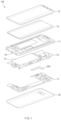
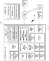
- FIG. 1 is an exploded perspective view of an electronic device.
- an electronic device 100 includes a side bezel structure 11, a first support member 16 (e.g., a bracket), a front plate 12, a display 13, a printed circuit board (PCB) 14, a battery 15, a 5G antenna module 200, a second support member 17 (e.g., a rear case), and a back plate 18.
- the electronic device 100 may not include a part (e.g., the first support member 16 or the second support member 17) of the components illustrated in FIG. 1 or may further include any other component not illustrated in FIG. 1 .
- the side bezel structure 11 may be combined with the front plate 12 and the back plate 18 to form a housing of the electronic device 100.
- the housing may form the exterior of the electronic device 100 and may protect components disposed in the electronic device 100 against an external environment (e.g., moisture or impact).
- the housing may include a first surface, a second surface facing away from the first surface, and a side surface surrounding a space between the first surface and the second surface.
- at least part of the front plate 12 may form the first surface of the housing.
- At least part of the back plate 18 may form the second surface of the housing.
- the side bezel structure 11 may form a side surface of the housing together with a portion of the front plate 12 and/or a portion of the back plate 18.
- the side surface may be understood as a region that surrounds a space between a first surface on which the front plate 12 is disposed and a second surface on which the back plate 18 is disposed.
- the side surface (e.g., a side surface 152 of FIG.
- the housing may include a first side region (e.g., a first side region 150-1 of FIG. 10A ) extending in a first direction, a second side region (e.g., a second side region 150-2 of FIG. 10A ) extending in a second direction perpendicular to the first direction from one end of the first side region, a third side region (e.g., a third side region 150-3 of FIG. 10A ) extending in the first direction from one end of the second side region, and a fourth side region extending in the second direction from one end of the third side region.
- At least part of the side bezel structure 11 may include a conductive region.
- the conductive region may be supplied with a power to cause an electromagnetic resonance.
- the electronic device 100 may receive or transmit a signal in a specified frequency band by using the electromagnetic resonance.
- the specified frequency band may be 600 MHz or higher and 6 GHz or lower.
- the first support member 16 may be disposed within the electronic device 100 so as to be connected with the side bezel structure 11 or may be integrally formed with the side bezel structure 11.
- the first support member 16 may support or fix electronic components disposed in the electronic device 100, for example, the PCB 14, electronic components disposed on the PCB 14, or various kinds of modules (e.g., the 5G antenna module 200) performing various functions in a direction of the front plate 12.
- the front plate 12 may be coupled to the side bezel structure 11 and the back plate 18 to form the housing.
- the front plate 12 may protect an internal component of the electronic device 100, for example, the display 13 against impact coming from a front surface of the electronic device 100.
- the front plate 12 may transmit a light generated from the display 13 or a light incident onto various kinds of sensors (e.g., an image sensor, an iris sensor, or a proximity sensor) disposed on the front surface of the electronic device 100.
- the display 13 may be disposed adjacent to one surface of the front plate 12.
- the display 13 may be electrically connected with the PCB 14 to output content (e.g., a text, an image, a video, an icon, a widget, or a symbol) or to receive a touch input (e.g., a touch, a gesture, or a hovering) from the user.
- content e.g., a text, an image, a video, an icon, a widget, or a symbol
- a touch input e.g., a touch, a gesture, or a hovering
- Various electronic components, various elements, or various printed circuits of the electronic device 100 may be mounted on the PCB 14.
- an application processor (AP), a communication processor (CP), or an intermediate frequency integrated circuit (IFIC), or a communication circuit may be mounted on the PCB 14.
- AP application processor
- CP communication processor
- IFIC intermediate frequency integrated circuit
- a communication circuit e.g., a second wireless communication circuit of FIG. 2
- the PCB 14 includes at least one or more ground regions.
- the ground region may be understood as a conductive region of a specified size or larger.
- the ground region is used as a ground for electronic components included in the PCB 14, for example, for an operation of a communication circuit.
- the PCB 14 may be referred to as a "first PCB", a “main PCB”, a “main board”, or a "printed board assembly (PBA)".
- the battery 15 may convert chemical energy and electrical energy bidirectionally.
- the battery 15 may convert chemical energy into electrical energy and may supply the converted electrical energy to the display 13 and various components or modules mounted on the PCB 14.
- a power management module for managing the charging and discharging of the battery 15 may be included in the PCB 14.
- the 5G antenna module 200 is disposed adjacent to the PCB 14.
- the 5G antenna module 200 may be physically connected with at least part of the PCB 14.
- the 5G antenna module 200 is disposed adjacent to the PCB 14, and is electrically connected with electronic components disposed on the PCB 14, for example, a communication module, a communication processor, or an application processor.
- the 5G antenna module 200 may transmit and receive RF signals through a part of the housing that is disposed adjacent to the 5G antenna module 200.
- the 5G antenna module 200 may be disposed adjacent to an inner side of the housing of the electronic device 100.
- the 5G antenna module 200 disclosed in the specification may be disposed adjacent to a side surface (e.g., first to fourth side regions) of the housing.
- the housing is formed in the shape of a rectangle or substantially a rectangle as illustrated in FIG. 1
- the 5G antenna module 200 may be disposed adjacent to each side surface of the housing.
- the 5G antenna module 200 may be disposed to be spaced from the center of the circle as much as a specified distance toward the side surface.
- the 5G antenna module 200 includes the antenna array.
- the 5G antenna module 200 may include a first surface facing in a first direction and a second surface facing away from the first direction.
- the antenna array may be formed on the first surface.
- the second support member 17 may be interposed between the back plate 18 and the PCB 14. Identically or similarly to the first support member 16, the second support member 17 may support or fix the electronic components in the electronic device 100 in a direction of the back plate 18.
- the back plate 18 may be coupled to the side bezel structure 11 and the front plate 12 to form the housing.
- the back plate 18 may protect internal components of the electronic device 100 against impact coming from the back surface of the electronic device 100.
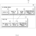
- FIG. 2 illustrates a block diagram of an electronic device, according to an embodiment
- the electronic device 100 includes the 5G antenna module 200 (e.g., the 5G antenna module 200 of FIG. 1 ) and a first printed circuit board (PCB) 110 (e.g., the PCB 14 of FIG. 1 ).
- the first printed circuit board 110 may be described as the first PCB 110.
- the first PCB 110 includes a non-conductive region 120 and a conductive region 125.
- the conductive region 125 functions as a ground region within the electronic device 100.
- the non-conductive region 120 is a region in which a metal member has been removed from the first PCB 110.
- a first wireless communication circuit 130 and an inter frequency integrated circuit (IFIC) are disposed in the conductive region 125 of the first PCB 110.
- the first wireless communication circuit 130 may be referred to as a "communication circuit" for feeding a legacy antenna.
- the first wireless communication circuit 130 may transmit and receive an RF signal including a frequency band of 6 GHz or less, using at least one conductive pattern or a conductive layer included in the electronic device 100 as a radiator.
- the RF signal transmitted and received by the first wireless communication circuit 130 is described as a first RF signal.
- the IFIC may process a signal in an intermediate frequency band of the 5G antenna module 200. It may be understood that a second wireless communication circuit 240 and the IFIC are a communication circuit for 5G communication. In various embodiments, the communication processor for the IFIC may be implemented separately from communication processors of the first wireless communication circuit 130 and the second wireless communication circuit 240.
- the 5G antenna module 200 includes a PCB 210 (hereinafter, a second PCB 210), a conductive layer 220, an antenna array 230, and the second wireless communication circuit 240.
- the second PCB 210 may be a main PCB included in the electronic device 100.
- the antenna array 230 includes a plurality of antenna elements.
- the second wireless communication circuit 240 generates an RF signal having at least one beam pattern by using the plurality of antenna elements included in the antenna array 230.
- the RF signal may include a millimeter wave signal including a signal in an ultra-high frequency band of, for example, 3 GHz to 300 GHz.
- the RF signal transmitted and received by the second wireless communication circuit 240 is described as a second RF signal.
- the 5G antenna module 200 including the antenna array 230 may form a beam pattern having directivity in a specific direction. Accordingly, the 5G antenna module 200 may transmit and receive a second RF signal.
- the second wireless communication circuit 240 may transmit and receive a second RF signal by changing a direction of a beam pattern of the antenna array 230.
- the second wireless communication circuit 240 may adjust the phase of the signal radiated from each of antenna elements.
- the beam pattern of the antenna array 230 may be changed based on a phase difference between signals radiated from each of the antenna elements included in the antenna array 230.
- the 5G antenna module 200 may have directivity in a direction of a side surface (e.g., the side bezel structure 11 of FIG. 1 ) of the housing, in a direction of a front surface (e.g., the front plate 12 of FIG. 1 ) of the housing, or in a direction of a back surface (e.g., the back plate 18 of FIG. 1 ) of the housing from the inside of the electronic device 100, depending on a location where the 5G antenna module 200 is disposed.
- a side surface e.g., the side bezel structure 11 of FIG. 1
- a front surface e.g., the front plate 12 of FIG. 1
- a back surface e.g., the back plate 18 of FIG. 1
- the second wireless communication circuit 240 is electrically connected to each of a plurality of antenna elements included in the antenna array 230.
- the second wireless communication circuit 240 may provide a specific amount of current to the antenna elements through a feeding line connected to the plurality of antenna elements included in the antenna array 230.
- the conductive layer 220 operates as a ground region for the 5G antenna module 200.
- the second wireless communication circuit 240 may be electrically connected to one point of the conductive layer 220.
- the conductive layer 220 may perform a shielding function on the 5G antenna module 200.
- the conductive layer 220 is a shield can or a shielding layer.
- the conductive layer 220 may be disposed in a region corresponding to a region in which the second wireless communication circuit 240 on the second PCB 210 is disposed.
- the conductive layer 220 may perform a shielding function on the electrical signal inside the electronic device 100 with respect to the second wireless communication circuit 240.
- the conductive layer 220 may operate as a radiator of a legacy antenna of the electronic device 100.
- the first wireless communication circuit 130 is electrically connected to one point of the conductive layer 220. It may be understood that the one point (hereinafter, a first point) is a feeding point for the legacy antenna.
- the first wireless communication circuit 130 may transmit and receive a first RF signal through an electrical path formed in at least part of the conductive layer 220 by feeding the first point of the conductive layer 220.
- the first wireless communication circuit 130 may be a communication circuit for WiFi communication, Bluetooth communication, or 4G communication.
- the electronic device 100 may further include a configuration not illustrated in FIG. 2 .
- the electronic device 100 may further include at least one processor (e.g., a processor 1240 of FIG. 12 ) electrically connected to the first wireless communication circuit 130 and/or the second wireless communication circuit 240.
- the at least one processor may include an application processor and/or a communication processor.
- the at least one processor may control operations of the first wireless communication circuit 130 and/or the second wireless communication circuit 240. It may be understood that the operations of the first wireless communication circuit 130 and the second wireless communication circuit 240 to be described later are operations of the at least one processor.
- the description given with reference to FIG. 2 may be identically applied to components having the same reference numerals/marks as the components of the electronic device 100 described with reference to FIG. 2 .
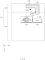
- FIG. 3 is an inner perspective view of an electronic device including a 5G antenna module, according to an embodiment.
- the arrangement structure of illustrated in FIG. 3 is shown as an example.
- the first PCB 110 and the 5G antenna module 200 may be arranged differently from FIG. 3 .
- the first PCB 110 includes the conductive region 125 and the non-conductive region 120.
- communication circuits including the first wireless communication circuit 130 and the IFIC are disposed in the conductive region 125. At least part of the conductive region 125 may operate as a ground of a legacy antenna.
- the conductive region 125 of the first PCB 110 may include a plurality of conductive layers.
- the 5G antenna module 200 may be disposed parallel to the first PCB 110.
- the predetermined angle may vary depending on a shape of the housing of the electronic device 100.
- the first portion 212 and the second portion 214 may be disposed adjacent to a side surface (e.g., the side bezel structure 11 of FIG. 1 ) of the housing of the electronic device 100.
- the first portion 212 and the second portion 214 may be disposed to have a substantially right angle. This is illustrated as an example in FIGS. 3 and 6 .
- the 5G antenna module 200 includes the conductive layer 220 (not illustrated).
- the first wireless communication circuit e.g., the first wireless communication circuit 130 of FIG. 2
- the first wireless communication circuit 130 is configured to transmit and receive a first RF signal, using at least part of the conductive region 125 of the first PCB 110 and the conductive layer 220.
- a feed point for the legacy antenna is the first point 132a of the conductive layer 220 included in the first portion 212.
- the conductive region 125 of the first PCB 110 may operate as a ground for the legacy antenna. At least part of the conductive layer 220 included in the first portion 212 may operate as a radiator of a legacy antenna.
- the first wireless communication circuit 130 may transmit and receive a first RF signal based on an electrical path formed by the first point 132a and a ground point 132b electrically connected to the conductive region 125.
- the conductive patch 411 may be a conductive material that is supplied with a power from the second wireless communication circuit 240 to cause an electromagnetic resonance.
- the coupling conductive patch 412 that is a conductive material may guide a direction of an electromagnetic signal radiated from the conductive patch 411 supplied with the power.
- At least part of the conductive layer included in the 5G antenna module 200-1 may operate as a radiator of a legacy antenna.
- at least part of the conductive layer included in the first sub PCB 210-1 and at least part of the conductive layer included in the second sub PCB 210-2 may operate as radiators of a legacy antenna.
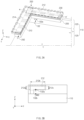
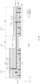
- a cross-sectional view of the 5G antenna module 200-1 (e.g., the 5G antenna module 200 of FIG. 7 ) includes the FPCB 215.
- the cross-sectional view of FIG. 9B is a cross-sectional view of the 5G antenna module 200-1 that is viewed based on line w-w' of FIG. 9A .
- the first sub PCB 210-1, the second sub PCB 210-2, and the FPCB 215 may have a layer structure.
- the 5G antenna module 200-1 may include a first layer structure 410c_1 of the first sub PCB 210-1 disposed in a first region 41, a second layer structure 410c_2 of the second sub PCB 210-2 disposed in a second region 42, and a third layer structure 410c_3 of the FPCB 215 disposed in a third region 43.
- the second wireless communication circuit 240 may be disposed on one surface of the second sub PCB 210-2.
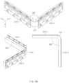
- FIG. 10A is an inner perspective view of an electronic device, according to various embodiments.
- FIG. 10B is a three-dimensional view of a 5G antenna module according to various embodiments.
- the conductive layer 220 included in the first sub PCB 210-1 may be supplied with a power by the first wireless communication circuit 130 (the direction 132). At least part of the conductive layer 220 included in the first sub PCB 210-1 may operate as a radiator of a legacy antenna.
- the electronic device 1101 in the network environment 1100 may communicate with an electronic device 1102 via a first network 1198 (e.g., a short-range wireless communication network), or an electronic device 1104 or a server 1108 via a second network 1199 (e.g., a long-range wireless communication network).
- the electronic device 1101 may communicate with the electronic device 1104 via the server 1108.
- the processor 1120 may execute, for example, software (e.g., a program 1140) to control at least one other component (e.g., a hardware or software component) of the electronic device 1101 coupled with the processor 1120, and may perform various data processing or computation. As at least part of the data processing or computation, the processor 1120 may load a command or data received from another component (e.g., the sensor module 1176 or the communication module 1190) in volatile memory 1132, process the command or the data stored in the volatile memory 1132, and store resulting data in non-volatile memory 1134.
- software e.g., a program 1140
- the processor 1120 may load a command or data received from another component (e.g., the sensor module 1176 or the communication module 1190) in volatile memory 1132, process the command or the data stored in the volatile memory 1132, and store resulting data in non-volatile memory 1134.
- the input device 1150 may receive a command or data to be used by other component (e.g., the processor 1120) of the electronic device 1101, from the outside (e.g., a user) of the electronic device 1101.
- the input device 1150 may include, for example, a microphone, a mouse, a keyboard, or a digital pen (e.g., a stylus pen).
- the sound output device 1155 may output sound signals to the outside of the electronic device 1101.
- the sound output device 1155 may include, for example, a speaker or a receiver.
- the speaker may be used for general purposes, such as playing multimedia or playing record, and the receiver may be used for an incoming calls.
- the receiver may be implemented as separate from, or as part of the speaker.
- the display device 1160 may visually provide information to the outside (e.g., a user) of the electronic device 1101.
- the display device 1160 may include, for example, a display, a hologram device, or a projector and control circuitry to control a corresponding one of the display, hologram device, and projector.
- the display device 1160 may include touch circuitry adapted to detect a touch, or sensor circuitry (e.g., a pressure sensor) adapted to measure the intensity of force incurred by the touch.
- the sensor module 1176 may detect an operational state (e.g., power or temperature) of the electronic device 1101 or an environmental state (e.g., a state of a user) external to the electronic device 1101, and then generate an electrical signal or data value corresponding to the detected state.
- the sensor module 1176 may include, for example, a gesture sensor, a gyro sensor, an atmospheric pressure sensor, a magnetic sensor, an acceleration sensor, a grip sensor, a proximity sensor, a color sensor, an infrared (IR) sensor, a biometric sensor, a temperature sensor, a humidity sensor, or an illuminance sensor.
- the interface 1177 may support one or more specified protocols to be used for the electronic device 1101 to be coupled with the external electronic device (e.g., the electronic device 1102) directly (e.g., wiredly) or wirelessly.
- the interface 1177 may include, for example, a high definition multimedia interface (HDMI), a universal serial bus (USB) interface, a secure digital (SD) card interface, or an audio interface.
- HDMI high definition multimedia interface
- USB universal serial bus
- SD secure digital
- a connecting terminal 1178 may include a connector via which the electronic device 1101 may be physically connected with the external electronic device (e.g., the electronic device 1102).
- the connecting terminal 1178 may include, for example, a HDMI connector, a USB connector, a SD card connector, or an audio connector (e.g., a headphone connector).
- the haptic module 1179 may convert an electrical signal into a mechanical stimulus (e.g., a vibration or a movement) or electrical stimulus which may be recognized by a user via his tactile sensation or kinesthetic sensation.
- the haptic module 1179 may include, for example, a motor, a piezoelectric element, or an electric stimulator.
- the camera module 1180 may capture a still image or moving images.
- the camera module 1180 may include one or more lenses, image sensors, image signal processors, or flashes.
- the communication module 1190 may include a wireless communication module 1192 (e.g., a cellular communication module, a short-range wireless communication module, or a global navigation satellite system (GNSS) communication module) or a wired communication module 1194 (e.g., a local area network (LAN) communication module or a power line communication (PLC) module).
- a wireless communication module 1192 e.g., a cellular communication module, a short-range wireless communication module, or a global navigation satellite system (GNSS) communication module
- GNSS global navigation satellite system
- wired communication module 1194 e.g., a local area network (LAN) communication module or a power line communication (PLC) module.
- LAN local area network
- PLC power line communication
- an electronic device 1200 may include a housing 1210, a processor 1240 (e.g., the processor 1120 of FIG. 11 ), a communication module 1250 (e.g., the communication module 1190 of FIG. 11 ), a first communication device 1221, a second communication device 1222, a third communication device 1223, a fourth communication device 1224, a first conductive line 1231, a second conductive line 1232, a third conductive line 1233, or a fourth conductive line 1234.
- the first communication device 1221, the second communication device 1222, the third communication device 1223, and the fourth communication device 1224 may correspond to the 5G antenna module 200 of FIG. 2 .
- the electronic device 1200 may include at least one communication device.
- the electronic device 1200 may include at least one of the first communication device 1221, the second communication device 1222, the third communication device 1223, or the fourth communication device 1224.
- FIG. 13 is a block diagram of a communication device according to an embodiment.
- a communication device 1300 (e.g., the 5G antenna module 200 of FIG. 2 , the first communication device 1221, the second communication device 1222, the third communication device 1223, or the fourth communication device 1224 of FIG. 12 ) includes a communication circuit 1330 (e.g., RFIC) (e.g., the second wireless communication circuit 240 of FIG. 2 ), a PCB 1350 (e.g., the second PCB 210 of FIG. 2 ), a first antenna array 1340, or a second antenna array 1345.
- the communication device 130 may be referred to as the "5G antenna module 200" of FIG. 2 or the "5G antenna module 200-1" of FIG. 9A .
- the first antenna array 1340 and the second antenna array 1345 may be referred to as the "antenna array" 230 of FIG. 2 .
- the communication circuit 1330, the first antenna array 1340, or the second antenna array 1345 are disposed on the PCB 1350.
- the first antenna array 1340 or the second antenna array 1345 may be disposed on a first surface of the PCB 1350
- the communication circuit 1330 may be disposed on a second surface of the PCB 1350.
- the PCB 1350 may include a connector (e.g., a coaxial cable connector or a board-to-board (B-to-B) connector) for electrical connection with any other PCB (e.g., a PCB on which the communication module 1250 of FIG. 12 is disposed), using a transmission line (e.g., the first conductive line 1231 of FIG. 12 or a coaxial cable).
- the PCB 1350 may be connected to the PCB, on which the communication module 1250 is disposed, using the coaxial cable connector, and the coaxial cable may be used to transfer a receive/transmit IF signal or an RF signal.
- a power or any other control signal may be delivered through the B-to-B connector.
- the first antenna array 1340 or the second antenna array 1345 may include a plurality of antenna elements.
- the antenna elements may include a patch antenna, a loop antenna, or a dipole antenna.
- an antenna element included in the first antenna array 1340 may be a patch antenna for forming a beam toward the back plate of the electronic device 1200.
- an antenna element included in the second antenna array 1345 may be a dipole antenna or a loop antenna to form a beam toward the side member of the electronic device 1200.
- the communication circuit 1330 may support at least part (e.g., 24 GHz to 30 GHz or 37 GHz to 40 GHz) of a band ranging from 24 GHz to 100 GHz.
- the communication circuit 1330 may up-convert or down-convert a frequency.
- the communication circuit 1330 included in the communication device 1300 e.g., the first communication device 1221 of FIG. 12
- the communication circuit 1330 included in the communication device 1300 may down-convert an RF signal (e.g., a millimeter wave signal) received through the first antenna array 1340 or the second antenna array 1345 into an IF signal and may transmit the IF signal to a communication module by using a conductive line.
- an RF signal e.g., a millimeter wave signal
- the performance of a 5G antenna module and the performance of an antenna supporting a conventional communication technology may be maintained at a specified level or higher, in a limited mounting space.
- an electronic device may be further miniaturized by using a mounting space efficiently. This may allow a user to make use of an electronic device that has a smaller size and more improved performance.
- similar reference numerals may be used to refer to similar or related elements. It is to be understood that a singular form of a noun corresponding to an item may include one or more of the things, unless the relevant context clearly indicates otherwise.
- each of such phrases as “A or B”, “at least one of A and B”, “at least one of A or B”, “A, B, or C”, “at least one of A, B, and C”, and “at least one of A, B, or C” may include any one of, or all possible combinations of the items enumerated together in a corresponding one of the phrases.
- such terms as “1st” and “2nd”, or “first” and “second” may be used to simply distinguish a corresponding component from another, and does not limit the components in other aspect (e.g., importance or order).
- an element e.g., a first element
- the element may be coupled with the other element directly (e.g., wiredly), wirelessly, or via a third element.
- the machine-readable storage medium may be provided in the form of a non-transitory storage medium.
- non-transitory simply means that the storage medium is a tangible device, and does not include a signal (e.g., an electromagnetic wave), but this term does not differentiate between where data is semi-permanently stored in the storage medium and where the data is temporarily stored in the storage medium.
- the computer program product may be traded as a product between a seller and a buyer.
- the computer program product may be distributed in the form of a machine-readable storage medium (e.g., compact disc read only memory (CD-ROM)), or be distributed (e.g., downloaded or uploaded) online via an application store (e.g., PlayStore TM ), or between two user devices (e.g., smart phones) directly. If distributed online, at least part of the computer program product may be temporarily generated or at least temporarily stored in the machine-readable storage medium, such as memory of the manufacturer's server, a server of the application store, or a relay server.
- CD-ROM compact disc read only memory
- an application store e.g., PlayStore TM
- two user devices e.g., smart phones
Landscapes
- Engineering & Computer Science (AREA)
- Signal Processing (AREA)
- Computer Networks & Wireless Communication (AREA)
- Microelectronics & Electronic Packaging (AREA)
- Support Of Aerials (AREA)
- Variable-Direction Aerials And Aerial Arrays (AREA)
Claims (15)
- Elektronische Vorrichtung (100), umfassend:eine erste Leiterplatte, PCB, (110), die einen nicht leitenden Bereich (120) und einen leitenden Bereich (125) enthält, der als eine Masse fungiert;eine erste drahtlose Kommunikationsschaltung (130), die auf der ersten PCB (110) angeordnet ist; undein Antennenmodul der 5. Generation, 5G-Antennenmodul, (200), das angrenzend an die erste PCB (110) angeordnet ist,wobei das 5G-Antennenmodul (200) Folgendes enthält:mindestens eine zweite PCB (210), die eine Antennenanordnung (230) und eine leitende Schicht (220) enthält, die als eine Masse der Antennenanordnung (230) fungiert; undeine zweite drahtlose Kommunikationsschaltung (240), die elektrisch mit der Antennenanordnung (230) verbunden ist,wobei die zweite PCB (210) einen ersten Abschnitt (212) und einen zweiten Abschnitt (214) enthält, der einen vorbestimmten Winkel zu dem ersten Abschnitt (212) aufweist, wobei der erste Abschnitt (212) angrenzend an den nicht leitenden Bereich (120) angeordnet ist und mindestens ein Teil des zweiten Abschnitts (214) angrenzend an den leitenden Bereich (125) angeordnet ist,wobei die erste drahtlose Kommunikationsschaltung (130) elektrisch mit einem ersten Punkt (132a) der leitenden Schicht (220) verbunden ist, der in dem ersten Abschnitt (212) enthalten ist, und dazu konfiguriert ist, ein erstes HF-Signal in einem ersten Frequenzband unter Verwendung des leitenden Bereichs (125) und mindestens eines Teils der leitenden Schicht (220) zu senden oder zu empfangen, undwobei die zweite drahtlose Kommunikationsschaltung (240) dazu konfiguriert ist, ein zweites HF-Signal in einem zweiten Frequenzband unter Verwendung der Antennenanordnung (230) zu senden oder zu empfangen.
- Elektronische Vorrichtung (100) nach Anspruch 1, wobei das erste Frequenzband ein Frequenzband von 6 GHz oder weniger enthält, und
wobei das zweite Frequenzband ein Frequenzband von 20 GHz oder höher enthält. - Elektronische Vorrichtung (100) nach Anspruch 1, ferner umfassend:ein Gehäuse (150), das eine erste Oberfläche, eine zweite Oberfläche, die von der ersten Oberfläche abgewandt ist, und eine Seitenoberfläche (152) enthält, die einen Raum zwischen der ersten Oberfläche und der zweiten Oberfläche umgibt,wobei die erste PCB (110), die erste drahtlose Kommunikationsschaltung (130) und das 5G-Antennenmodul (200) innerhalb des Gehäuses angeordnet sind.
- Elektronische Vorrichtung (100) nach Anspruch 3, wobei der erste Abschnitt (212) und der zweite Abschnitt (214) angrenzend an die Seitenoberfläche (152) des Gehäuses (150) angeordnet sind.
- Elektronische Vorrichtung nach Anspruch 4, wobei der erste Abschnitt (212) eine erste Seite (212a) angrenzend an den zweiten Abschnitt (214), eine zweite Seite (212b), die sich von einem Ende der ersten Seite (212a) und senkrecht zu der ersten Seite (212a) erstreckt, und eine dritte Seite (212c) enthält, die sich von einem Ende der zweiten Seite (212b) und parallel zu der ersten Seite (212a) erstreckt, und
wobei die erste drahtlose Kommunikationsschaltung (130) elektrisch mit dem ersten Punkt (132a) angrenzend an die erste Seite (212a) verbunden ist. - Elektronische Vorrichtung (100) nach Anspruch 4, wobei der erste Abschnitt (212) eine erste Seite (212a) angrenzend an den zweiten Abschnitt (214), eine zweite Seite (212b), die sich von einem Ende der ersten Seite (212a) und senkrecht zu der ersten Seite (212a) erstreckt, und eine dritte Seite (212c) enthält, die sich von einem Ende der zweiten Seite (212b) und parallel zu der ersten Seite (212a) erstreckt, und
wobei die erste drahtlose Kommunikationsschaltung (130) elektrisch mit dem ersten Punkt (132a) angrenzend an die dritte Seite (212c) verbunden ist. - Elektronische Vorrichtung (100) nach Anspruch 3, wobei die Seitenoberfläche (152) einen ersten Seitenbereich (150-1), der sich in einer ersten Richtung erstreckt, einen zweiten Seitenbereich (150-2), der sich in einer zweiten Richtung senkrecht zu der ersten Richtung von einem Ende des ersten Seitenbereichs (150-1) erstreckt, und einen dritten Seitenbereich (150-3) enthält, der sich in der zweiten Richtung von dem anderen Ende des ersten Seitenbereichs (150-1) erstreckt, und
wobei der erste Abschnitt (212) dem ersten Seitenbereich (150-1) entspricht und der zweite Abschnitt (214) dem zweiten Seitenbereich (150-2) entspricht. - Elektronische Vorrichtung (100) nach Anspruch 7, wobei die mindestens eine zweite PCB (210) eine erste Sub-PCB (210-1), die dem ersten Abschnitt (212) entspricht, und eine zweite Sub-PCB (210-2), die dem zweiten Abschnitt (214) entspricht, enthält,wobei das 5G-Antennenmodul (200) ferner eine flexible Leiterplatte, FPCB, (215) enthält, die zwischen der ersten Sub-PCB (210-1) und der zweiten Sub-PCB (210-2) eingefügt ist, undwobei die FPCB (215) in einer gekrümmten Weise angeordnet ist, um einer Ecke zwischen dem ersten Seitenbereich (150-1) und dem zweiten Seitenbereich (150-2) zu entsprechen.
- Elektronische Vorrichtung (100) nach Anspruch 1, wobei der leitende Bereich (125) elektrisch mit einem zweiten Punkt (132b) der leitenden Schicht (220) verbunden ist, der sich von dem ersten Punkt (132a) unterscheidet.
- Elektronische Vorrichtung (100) nach Anspruch 9, wobei die erste drahtlose Kommunikationsschaltung (130) zu Folgendem konfiguriert ist:
Senden oder Empfangen des ersten HF-Signals über einen elektrischen Pfad, der basierend auf dem ersten Punkt (132a) und dem zweiten Punkt (132b) ausgebildet ist. - Elektronische Vorrichtung (100) nach Anspruch 9, ferner umfassend:ein leitendes Element (225-1, 225-2), das in einem Bereich angeordnet ist, der der zweiten drahtlosen Kommunikationsschaltung (240) der zweiten PCB (210) entspricht,wobei die erste drahtlose Kommunikationsschaltung (130) elektrisch mit dem ersten Punkt (132a) oder einem Punkt des leitenden Elements (225-1, 225-2) verbunden ist.
- Elektronische Vorrichtung (100) nach Anspruch 11, wobei die erste drahtlose Kommunikationsschaltung (130) zu Folgendem konfiguriert ist:
Senden oder Empfangen des ersten HF-Signals über einen elektrischen Pfad, der basierend auf dem einen Punkt des leitenden Elements (225-1, 225-2) und dem zweiten Punkt (132b) ausgebildet ist. - Elektronische Vorrichtung (100) nach Anspruch 1, wobei der erste Abschnitt (212) und der zweite Abschnitt (214) im Wesentlichen senkrecht zueinander sind.
- Elektronische Vorrichtung (100) nach Anspruch 1, wobei die leitende Schicht (220) elektrisch mit einem leitenden Element (225-1, 225-2) verbunden ist und
wobei die erste drahtlose Kommunikationsschaltung (130) zu Folgendem konfiguriert ist:
Senden oder Empfangen des ersten HF-Signals über einen elektrischen Pfad, der durch den mindestens einen Teil der leitenden Schicht (220) und das leitende Element (225-1, 225-2) ausgebildet ist. - Elektronische Vorrichtung (100) nach Anspruch 8, wobei die erste Sub-PCB (210-1) und die zweite Sub-PCB (210-2) senkrecht zu der ersten PCB (110) angeordnet sind.
Applications Claiming Priority (2)
| Application Number | Priority Date | Filing Date | Title |
|---|---|---|---|
| KR1020180106738A KR102526400B1 (ko) | 2018-09-06 | 2018-09-06 | 5g 안테나 모듈을 포함하는 전자 장치 |
| PCT/KR2019/011333 WO2020050591A1 (ko) | 2018-09-06 | 2019-09-03 | 5g 안테나 모듈을 포함하는 전자 장치 |
Publications (3)
| Publication Number | Publication Date |
|---|---|
| EP3820126A1 EP3820126A1 (de) | 2021-05-12 |
| EP3820126A4 EP3820126A4 (de) | 2021-10-27 |
| EP3820126B1 true EP3820126B1 (de) | 2025-07-02 |
Family
ID=69722005
Family Applications (1)
| Application Number | Title | Priority Date | Filing Date |
|---|---|---|---|
| EP19856843.8A Active EP3820126B1 (de) | 2018-09-06 | 2019-09-03 | Elektronische vorrichtung mit 5g-antennenmodul |
Country Status (5)
| Country | Link |
|---|---|
| US (1) | US12081246B2 (de) |
| EP (1) | EP3820126B1 (de) |
| KR (1) | KR102526400B1 (de) |
| CN (1) | CN112640402B (de) |
| WO (1) | WO2020050591A1 (de) |
Families Citing this family (15)
| Publication number | Priority date | Publication date | Assignee | Title |
|---|---|---|---|---|
| KR102809525B1 (ko) | 2020-04-14 | 2025-05-19 | 삼성전자주식회사 | 안테나 모듈을 포함하는 전자 장치 |
| KR102865027B1 (ko) * | 2020-08-06 | 2025-09-26 | 삼성전자 주식회사 | 안테나 및 그것을 포함하는 전자 장치 |
| KR102765468B1 (ko) * | 2020-09-22 | 2025-02-12 | 삼성전자주식회사 | 복수의 안테나를 포함하는 전자 장치 |
| KR102752738B1 (ko) * | 2020-11-11 | 2025-01-10 | 삼성전자주식회사 | 하우징을 포함하는 전자 장치 |
| KR102525796B1 (ko) | 2021-04-16 | 2023-04-27 | (주)파트론 | 전자 장치 |
| CN113363705B (zh) * | 2021-04-30 | 2022-08-16 | 荣耀终端有限公司 | 移动终端设备 |
| CN117276254B (zh) * | 2021-06-30 | 2024-06-28 | 华为技术有限公司 | 天线结构、天线模组、芯片与电子设备 |
| KR20230006224A (ko) | 2021-07-02 | 2023-01-10 | 삼성전자주식회사 | 안테나를 포함하는 전자 장치 |
| KR20230007692A (ko) * | 2021-07-06 | 2023-01-13 | 삼성전자주식회사 | 안테나 및 그것을 포함하는 전자 장치 |
| US12316018B2 (en) | 2021-07-06 | 2025-05-27 | Samsung Electronics Co., Ltd. | Antenna and electronic device including the same |
| KR102546095B1 (ko) | 2021-10-14 | 2023-06-21 | (주)파트론 | 전자 장치 |
| US11791538B1 (en) * | 2022-03-25 | 2023-10-17 | Infineon Technologies Ag | Antenna in package arrangement |
| EP4593194A4 (de) * | 2022-11-14 | 2025-12-31 | Samsung Electronics Co Ltd | Antennenmodul und elektronische vorrichtung mit antennenmodul |
| CN117410674B (zh) * | 2023-11-17 | 2024-06-14 | 云谷(固安)科技有限公司 | 天线装置及无线移动终端 |
| WO2026059381A1 (ko) * | 2024-09-13 | 2026-03-19 | 삼성전자 주식회사 | 플렉서블 인쇄 회로 기판 및 이를 포함하는 전자 장치 |
Citations (1)
| Publication number | Priority date | Publication date | Assignee | Title |
|---|---|---|---|---|
| EP3816768A1 (de) * | 2018-05-22 | 2021-05-05 | Vivo Mobile Communication Co., Ltd. | Objekterkennungsverfahren und mobiles endgerät |
Family Cites Families (69)
| Publication number | Priority date | Publication date | Assignee | Title |
|---|---|---|---|---|
| KR20020022484A (ko) | 2000-09-20 | 2002-03-27 | 윤종용 | 이동통신 단말기의 내장형 이중대역 안테나 구현장치 및휩 안테나 연동방법 |
| JP4121860B2 (ja) * | 2001-05-17 | 2008-07-23 | サイプレス セミコンダクター コーポレーション | ボールグリッドアレイアンテナ |
| US7265719B1 (en) * | 2006-05-11 | 2007-09-04 | Ball Aerospace & Technologies Corp. | Packaging technique for antenna systems |
| JP4863109B2 (ja) | 2006-06-05 | 2012-01-25 | 日立金属株式会社 | チップアンテナ、アンテナ装置および通信機器 |
| KR100977036B1 (ko) * | 2008-05-01 | 2010-08-19 | 주식회사 모비텍 | 다층 구조의 다중 대역 칩 안테나 |
| KR101761280B1 (ko) | 2009-06-09 | 2017-07-25 | 삼성전자주식회사 | 휴대용 단말기의 지피에스용 내장형 안테나 장치 |
| KR101604759B1 (ko) * | 2009-09-04 | 2016-03-18 | 엘지전자 주식회사 | 안테나 어셈블리 및 이를 갖는 이동 단말기 |
| KR20110078048A (ko) | 2009-12-30 | 2011-07-07 | 엘지전자 주식회사 | 휴대 단말기 |
| US9905922B2 (en) * | 2011-08-31 | 2018-02-27 | Qualcomm Incorporated | Wireless device with 3-D antenna system |
| KR101708311B1 (ko) * | 2012-06-21 | 2017-02-20 | 엘지전자 주식회사 | 안테나 장치 및 이를 구비하는 이동 단말기 |
| JP6016556B2 (ja) | 2012-09-26 | 2016-10-26 | 京セラ株式会社 | 携帯通信端末 |
| WO2014097969A1 (ja) | 2012-12-21 | 2014-06-26 | 株式会社村田製作所 | インタフェースユニット及びコンピュータ |
| US20150070219A1 (en) | 2013-09-06 | 2015-03-12 | Apple Inc. | Hybrid antenna for a personal electronic device |
| US9806422B2 (en) * | 2013-09-11 | 2017-10-31 | International Business Machines Corporation | Antenna-in-package structures with broadside and end-fire radiations |
| US9531087B2 (en) * | 2013-10-31 | 2016-12-27 | Sony Corporation | MM wave antenna array integrated with cellular antenna |
| US9773742B2 (en) * | 2013-12-18 | 2017-09-26 | Intel Corporation | Embedded millimeter-wave phased array module |
| CN104953276A (zh) * | 2014-03-26 | 2015-09-30 | 联想(北京)有限公司 | 一种通讯电子设备及其天线装置 |
| TWI530020B (zh) * | 2014-07-17 | 2016-04-11 | 鋐寶科技股份有限公司 | 天線系統 |
| KR102305975B1 (ko) * | 2014-10-22 | 2021-09-28 | 삼성전자주식회사 | 무선 기기의 안테나 장치 |
| US10725150B2 (en) * | 2014-12-23 | 2020-07-28 | Infineon Technologies Ag | System and method for radar |
| KR102352490B1 (ko) | 2015-06-11 | 2022-01-18 | 삼성전자주식회사 | 안테나 및 이를 구비한 전자 장치 |
| US10270186B2 (en) * | 2015-08-31 | 2019-04-23 | Kabushiki Kaisha Toshiba | Antenna module and electronic device |
| CN205029703U (zh) * | 2015-09-10 | 2016-02-10 | 上海卓易科技股份有限公司 | 一种改善手机wifi信号的手机套及手机 |
| US20170110787A1 (en) | 2015-10-14 | 2017-04-20 | Apple Inc. | Electronic Devices With Millimeter Wave Antennas And Metal Housings |
| JP6451865B2 (ja) * | 2015-10-14 | 2019-01-16 | 株式会社村田製作所 | アンテナ装置 |
| KR102507472B1 (ko) | 2016-02-26 | 2023-03-09 | 삼성전자주식회사 | 디스플레이를 구비한 전자 장치의 안테나 |
| US9628115B1 (en) | 2016-04-08 | 2017-04-18 | Htc Corporation | Wireless communication device |
| CN107395788B (zh) | 2016-05-17 | 2021-03-23 | 北京小米移动软件有限公司 | 终端壳体及终端 |
| US10998622B2 (en) | 2016-07-21 | 2021-05-04 | Samsung Electronics Co., Ltd | Antenna for wireless communication and electronic device including the same |
| KR102332117B1 (ko) | 2016-07-21 | 2021-11-30 | 삼성전자주식회사 | 무선 통신을 위한 안테나 및 이를 포함하는 전자 장치 |
| US10418687B2 (en) * | 2016-07-22 | 2019-09-17 | Apple Inc. | Electronic device with millimeter wave antennas on printed circuits |
| KR102509520B1 (ko) | 2016-07-29 | 2023-03-16 | 삼성전자주식회사 | 안테나를 포함하는 전자 장치 |
| KR102532660B1 (ko) | 2016-09-19 | 2023-05-16 | 삼성전자주식회사 | 안테나를 포함하는 전자 장치 |
| CN106450773A (zh) | 2016-09-29 | 2017-02-22 | 宇龙计算机通信科技(深圳)有限公司 | 金属后盖及移动终端 |
| WO2018081146A1 (en) * | 2016-10-24 | 2018-05-03 | Anokiwave, Inc. | Beamforming integrated circuit with rf grounded material ring and integral thermal mass |
| EP3537536A4 (de) * | 2016-11-01 | 2020-06-10 | LG Electronics Inc. -1- | Mobiles endgerät |
| KR102542594B1 (ko) * | 2016-12-16 | 2023-06-14 | 삼성전자 주식회사 | 다층 인쇄 회로 기판 및 이를 포함하는 전자 장치 |
| WO2018119153A2 (en) * | 2016-12-21 | 2018-06-28 | Intel Corporation | Wireless communication technology, apparatuses, and methods |
| TWI859783B (zh) * | 2016-12-29 | 2024-10-21 | 美商天工方案公司 | 前端系統、無線通信裝置及封裝前端模組 |
| US10515924B2 (en) * | 2017-03-10 | 2019-12-24 | Skyworks Solutions, Inc. | Radio frequency modules |
| US11329364B2 (en) * | 2017-03-15 | 2022-05-10 | Sony Mobile Communications Inc. | Communication apparatus |
| US20180294558A1 (en) * | 2017-04-07 | 2018-10-11 | Skyworks Solutions, Inc. | Radio-frequency module with integrated conformal shield antenna |
| JP6946466B2 (ja) * | 2017-05-12 | 2021-10-06 | ホアウェイ・テクノロジーズ・カンパニー・リミテッド | 通信デバイス |
| CN110785893B (zh) * | 2017-06-14 | 2021-06-11 | 株式会社村田制作所 | 天线模块和通信装置 |
| WO2019008913A1 (ja) * | 2017-07-06 | 2019-01-10 | 株式会社村田製作所 | アンテナモジュール |
| KR102352592B1 (ko) * | 2017-07-13 | 2022-01-19 | 삼성전자주식회사 | 어레이 안테나를 포함하는 전자 장치 |
| US10476136B2 (en) * | 2017-07-20 | 2019-11-12 | Apple Inc. | Electronic device with speaker port aligned antennas |
| CN110998974B (zh) * | 2017-07-31 | 2022-03-15 | 株式会社村田制作所 | 天线模块和通信装置 |
| CN107768842B (zh) | 2017-09-14 | 2023-10-17 | 深圳市信维通信股份有限公司 | 一种用于5g移动通信的天线单元以及阵列天线 |
| US10854994B2 (en) * | 2017-09-21 | 2020-12-01 | Peraso Technolgies Inc. | Broadband phased array antenna system with hybrid radiating elements |
| US11245175B2 (en) * | 2017-09-30 | 2022-02-08 | Qualcomm Incorporated | Antenna module configurations |
| US10680661B2 (en) * | 2017-12-11 | 2020-06-09 | Microsoft Technology Licensing, Llc | Monopole and slot antenna assembly |
| JP7000864B2 (ja) * | 2018-01-05 | 2022-02-04 | 富士通株式会社 | アンテナ装置、及び、無線通信装置 |
| CN108448230B (zh) * | 2018-01-25 | 2020-12-15 | 瑞声科技(南京)有限公司 | 天线系统及通讯终端 |
| US11381003B2 (en) * | 2018-01-26 | 2022-07-05 | Sony Corporation | Antenna device |
| US10389021B1 (en) * | 2018-02-15 | 2019-08-20 | Intel Corporation | Antenna ports decoupling technique |
| US10971819B2 (en) * | 2018-02-16 | 2021-04-06 | Qualcomm Incorporated | Multi-band wireless signaling |
| US20190260110A1 (en) * | 2018-02-20 | 2019-08-22 | Intel Corporation | Antenna modules and communication devices |
| CN111742447B (zh) * | 2018-02-22 | 2021-07-23 | 株式会社村田制作所 | 天线模块和搭载有天线模块的通信装置 |
| US10084241B1 (en) * | 2018-02-23 | 2018-09-25 | Qualcomm Incorporated | Dual-polarization antenna system |
| WO2019174007A1 (zh) * | 2018-03-15 | 2019-09-19 | 华为技术有限公司 | 连接板、电路板组件及电子设备 |
| WO2019198870A1 (ko) * | 2018-04-09 | 2019-10-17 | 엘지전자 주식회사 | 연성인쇄회로기판 및 이를 포함하는 이동 단말기 |
| US10797394B2 (en) * | 2018-06-05 | 2020-10-06 | Intel Corporation | Antenna modules and communication devices |
| KR102514474B1 (ko) * | 2018-07-13 | 2023-03-28 | 삼성전자주식회사 | 안테나 구조체 및 안테나를 포함하는 전자 장치 |
| US20200021010A1 (en) * | 2018-07-13 | 2020-01-16 | Qualcomm Incorporated | Air coupled superstrate antenna on device housing |
| KR102500361B1 (ko) * | 2018-07-26 | 2023-02-16 | 삼성전자주식회사 | 5g 안테나 모듈을 포함하는 전자 장치 |
| JP7047918B2 (ja) * | 2018-08-06 | 2022-04-05 | 株式会社村田製作所 | アンテナモジュール |
| US11133574B2 (en) * | 2018-10-16 | 2021-09-28 | Murata Manufacturing Co., Ltd. | Communication device |
| WO2022138045A1 (ja) * | 2020-12-23 | 2022-06-30 | 株式会社村田製作所 | アンテナモジュールおよびそれを搭載した通信装置 |
-
2018
- 2018-09-06 KR KR1020180106738A patent/KR102526400B1/ko active Active
-
2019
- 2019-09-03 CN CN201980057130.XA patent/CN112640402B/zh active Active
- 2019-09-03 EP EP19856843.8A patent/EP3820126B1/de active Active
- 2019-09-03 WO PCT/KR2019/011333 patent/WO2020050591A1/ko not_active Ceased
- 2019-09-03 US US17/268,753 patent/US12081246B2/en active Active
Patent Citations (1)
| Publication number | Priority date | Publication date | Assignee | Title |
|---|---|---|---|---|
| EP3816768A1 (de) * | 2018-05-22 | 2021-05-05 | Vivo Mobile Communication Co., Ltd. | Objekterkennungsverfahren und mobiles endgerät |
Also Published As
| Publication number | Publication date |
|---|---|
| US12081246B2 (en) | 2024-09-03 |
| KR20200028256A (ko) | 2020-03-16 |
| US20220200640A1 (en) | 2022-06-23 |
| CN112640402B (zh) | 2022-11-22 |
| EP3820126A1 (de) | 2021-05-12 |
| CN112640402A (zh) | 2021-04-09 |
| WO2020050591A1 (ko) | 2020-03-12 |
| EP3820126A4 (de) | 2021-10-27 |
| KR102526400B1 (ko) | 2023-04-28 |
Similar Documents
| Publication | Publication Date | Title |
|---|---|---|
| EP3820126B1 (de) | Elektronische vorrichtung mit 5g-antennenmodul | |
| US12237568B2 (en) | Electronic device including 5G antenna module | |
| US11450949B2 (en) | Antenna structure and electronic device comprising antenna | |
| US12249756B2 (en) | Electronic device and method comprising antenna | |
| US12212063B2 (en) | Dual band antenna and electronic device including the same | |
| US11011828B2 (en) | Apparatus and method for arranging antennas supporting millimeter wave frequency bands | |
| US11081808B2 (en) | Antenna having radiation structure of given direction and electronic device including same | |
| US11228120B2 (en) | Antenna and electronic device including the same | |
| US11088438B2 (en) | Antenna using slot and electronic device including the same | |
| US10985463B2 (en) | Loop type antenna and electronic device including same | |
| US11705619B2 (en) | Antenna and electronic device including the same | |
| US12074361B2 (en) | Electronic device comprising antenna |
Legal Events
| Date | Code | Title | Description |
|---|---|---|---|
| STAA | Information on the status of an ep patent application or granted ep patent |
Free format text: STATUS: THE INTERNATIONAL PUBLICATION HAS BEEN MADE |
|
| PUAI | Public reference made under article 153(3) epc to a published international application that has entered the european phase |
Free format text: ORIGINAL CODE: 0009012 |
|
| STAA | Information on the status of an ep patent application or granted ep patent |
Free format text: STATUS: REQUEST FOR EXAMINATION WAS MADE |
|
| 17P | Request for examination filed |
Effective date: 20210208 |
|
| AK | Designated contracting states |
Kind code of ref document: A1 Designated state(s): AL AT BE BG CH CY CZ DE DK EE ES FI FR GB GR HR HU IE IS IT LI LT LU LV MC MK MT NL NO PL PT RO RS SE SI SK SM TR |
|
| REG | Reference to a national code |
Free format text: PREVIOUS MAIN CLASS: H04M0001020000 Ipc: H01Q0001240000 Ref country code: DE Ref legal event code: R079 Ref document number: 602019072080 Country of ref document: DE Free format text: PREVIOUS MAIN CLASS: H04M0001020000 Ipc: H01Q0001240000 |
|
| A4 | Supplementary search report drawn up and despatched |
Effective date: 20210924 |
|
| RIC1 | Information provided on ipc code assigned before grant |
Ipc: H04M 1/02 20060101ALI20210920BHEP Ipc: H04B 1/40 20150101ALI20210920BHEP Ipc: H01Q 21/28 20060101ALI20210920BHEP Ipc: H01Q 21/20 20060101ALI20210920BHEP Ipc: H01Q 9/04 20060101ALI20210920BHEP Ipc: H01Q 1/38 20060101ALI20210920BHEP Ipc: H01Q 1/22 20060101ALI20210920BHEP Ipc: H01Q 1/24 20060101AFI20210920BHEP |
|
| DAV | Request for validation of the european patent (deleted) | ||
| DAX | Request for extension of the european patent (deleted) | ||
| STAA | Information on the status of an ep patent application or granted ep patent |
Free format text: STATUS: EXAMINATION IS IN PROGRESS |
|
| 17Q | First examination report despatched |
Effective date: 20230316 |
|
| GRAP | Despatch of communication of intention to grant a patent |
Free format text: ORIGINAL CODE: EPIDOSNIGR1 |
|
| STAA | Information on the status of an ep patent application or granted ep patent |
Free format text: STATUS: GRANT OF PATENT IS INTENDED |
|
| INTG | Intention to grant announced |
Effective date: 20250131 |
|
| RAP3 | Party data changed (applicant data changed or rights of an application transferred) |
Owner name: SAMSUNG ELECTRONICS CO., LTD. |
|
| GRAS | Grant fee paid |
Free format text: ORIGINAL CODE: EPIDOSNIGR3 |
|
| GRAA | (expected) grant |
Free format text: ORIGINAL CODE: 0009210 |
|
| STAA | Information on the status of an ep patent application or granted ep patent |
Free format text: STATUS: THE PATENT HAS BEEN GRANTED |
|
| AK | Designated contracting states |
Kind code of ref document: B1 Designated state(s): AL AT BE BG CH CY CZ DE DK EE ES FI FR GB GR HR HU IE IS IT LI LT LU LV MC MK MT NL NO PL PT RO RS SE SI SK SM TR |
|
| REG | Reference to a national code |
Ref country code: GB Ref legal event code: FG4D |
|
| REG | Reference to a national code |
Ref country code: CH Ref legal event code: EP |
|
| REG | Reference to a national code |
Ref country code: DE Ref legal event code: R096 Ref document number: 602019072080 Country of ref document: DE |
|
| REG | Reference to a national code |
Ref country code: IE Ref legal event code: FG4D |
|
| PGFP | Annual fee paid to national office [announced via postgrant information from national office to epo] |
Ref country code: DE Payment date: 20250820 Year of fee payment: 7 |
|
| PGFP | Annual fee paid to national office [announced via postgrant information from national office to epo] |
Ref country code: GB Payment date: 20250820 Year of fee payment: 7 |
|
| REG | Reference to a national code |
Ref country code: NL Ref legal event code: MP Effective date: 20250702 |
|
| PG25 | Lapsed in a contracting state [announced via postgrant information from national office to epo] |
Ref country code: PT Free format text: LAPSE BECAUSE OF FAILURE TO SUBMIT A TRANSLATION OF THE DESCRIPTION OR TO PAY THE FEE WITHIN THE PRESCRIBED TIME-LIMIT Effective date: 20251103 |
|
| PG25 | Lapsed in a contracting state [announced via postgrant information from national office to epo] |
Ref country code: NL Free format text: LAPSE BECAUSE OF FAILURE TO SUBMIT A TRANSLATION OF THE DESCRIPTION OR TO PAY THE FEE WITHIN THE PRESCRIBED TIME-LIMIT Effective date: 20250702 |
|
| REG | Reference to a national code |
Ref country code: AT Ref legal event code: MK05 Ref document number: 1810353 Country of ref document: AT Kind code of ref document: T Effective date: 20250702 |
|
| PG25 | Lapsed in a contracting state [announced via postgrant information from national office to epo] |
Ref country code: IS Free format text: LAPSE BECAUSE OF FAILURE TO SUBMIT A TRANSLATION OF THE DESCRIPTION OR TO PAY THE FEE WITHIN THE PRESCRIBED TIME-LIMIT Effective date: 20251102 |
|
| PG25 | Lapsed in a contracting state [announced via postgrant information from national office to epo] |
Ref country code: NO Free format text: LAPSE BECAUSE OF FAILURE TO SUBMIT A TRANSLATION OF THE DESCRIPTION OR TO PAY THE FEE WITHIN THE PRESCRIBED TIME-LIMIT Effective date: 20251002 |
|
| REG | Reference to a national code |
Ref country code: LT Ref legal event code: MG9D |
|
| PG25 | Lapsed in a contracting state [announced via postgrant information from national office to epo] |
Ref country code: AT Free format text: LAPSE BECAUSE OF FAILURE TO SUBMIT A TRANSLATION OF THE DESCRIPTION OR TO PAY THE FEE WITHIN THE PRESCRIBED TIME-LIMIT Effective date: 20250702 |
|
| PG25 | Lapsed in a contracting state [announced via postgrant information from national office to epo] |
Ref country code: FI Free format text: LAPSE BECAUSE OF FAILURE TO SUBMIT A TRANSLATION OF THE DESCRIPTION OR TO PAY THE FEE WITHIN THE PRESCRIBED TIME-LIMIT Effective date: 20250702 |
|
| PG25 | Lapsed in a contracting state [announced via postgrant information from national office to epo] |
Ref country code: HR Free format text: LAPSE BECAUSE OF FAILURE TO SUBMIT A TRANSLATION OF THE DESCRIPTION OR TO PAY THE FEE WITHIN THE PRESCRIBED TIME-LIMIT Effective date: 20250702 |
|
| PG25 | Lapsed in a contracting state [announced via postgrant information from national office to epo] |
Ref country code: GR Free format text: LAPSE BECAUSE OF FAILURE TO SUBMIT A TRANSLATION OF THE DESCRIPTION OR TO PAY THE FEE WITHIN THE PRESCRIBED TIME-LIMIT Effective date: 20251003 |
|
| PG25 | Lapsed in a contracting state [announced via postgrant information from national office to epo] |
Ref country code: CZ Free format text: LAPSE BECAUSE OF FAILURE TO SUBMIT A TRANSLATION OF THE DESCRIPTION OR TO PAY THE FEE WITHIN THE PRESCRIBED TIME-LIMIT Effective date: 20250702 Ref country code: SE Free format text: LAPSE BECAUSE OF FAILURE TO SUBMIT A TRANSLATION OF THE DESCRIPTION OR TO PAY THE FEE WITHIN THE PRESCRIBED TIME-LIMIT Effective date: 20250702 |
|
| PG25 | Lapsed in a contracting state [announced via postgrant information from national office to epo] |
Ref country code: LV Free format text: LAPSE BECAUSE OF FAILURE TO SUBMIT A TRANSLATION OF THE DESCRIPTION OR TO PAY THE FEE WITHIN THE PRESCRIBED TIME-LIMIT Effective date: 20250702 |
|
| PG25 | Lapsed in a contracting state [announced via postgrant information from national office to epo] |
Ref country code: BG Free format text: LAPSE BECAUSE OF FAILURE TO SUBMIT A TRANSLATION OF THE DESCRIPTION OR TO PAY THE FEE WITHIN THE PRESCRIBED TIME-LIMIT Effective date: 20250702 Ref country code: PL Free format text: LAPSE BECAUSE OF FAILURE TO SUBMIT A TRANSLATION OF THE DESCRIPTION OR TO PAY THE FEE WITHIN THE PRESCRIBED TIME-LIMIT Effective date: 20250702 |
|
| PG25 | Lapsed in a contracting state [announced via postgrant information from national office to epo] |
Ref country code: RS Free format text: LAPSE BECAUSE OF FAILURE TO SUBMIT A TRANSLATION OF THE DESCRIPTION OR TO PAY THE FEE WITHIN THE PRESCRIBED TIME-LIMIT Effective date: 20251002 |
|
| PG25 | Lapsed in a contracting state [announced via postgrant information from national office to epo] |
Ref country code: ES Free format text: LAPSE BECAUSE OF FAILURE TO SUBMIT A TRANSLATION OF THE DESCRIPTION OR TO PAY THE FEE WITHIN THE PRESCRIBED TIME-LIMIT Effective date: 20250702 |
|
| PG25 | Lapsed in a contracting state [announced via postgrant information from national office to epo] |
Ref country code: RO Free format text: LAPSE BECAUSE OF FAILURE TO SUBMIT A TRANSLATION OF THE DESCRIPTION OR TO PAY THE FEE WITHIN THE PRESCRIBED TIME-LIMIT Effective date: 20250702 |
|
| PG25 | Lapsed in a contracting state [announced via postgrant information from national office to epo] |
Ref country code: SM Free format text: LAPSE BECAUSE OF FAILURE TO SUBMIT A TRANSLATION OF THE DESCRIPTION OR TO PAY THE FEE WITHIN THE PRESCRIBED TIME-LIMIT Effective date: 20250702 |
|
| PG25 | Lapsed in a contracting state [announced via postgrant information from national office to epo] |
Ref country code: DK Free format text: LAPSE BECAUSE OF FAILURE TO SUBMIT A TRANSLATION OF THE DESCRIPTION OR TO PAY THE FEE WITHIN THE PRESCRIBED TIME-LIMIT Effective date: 20250702 |
|
| PG25 | Lapsed in a contracting state [announced via postgrant information from national office to epo] |
Ref country code: IT Free format text: LAPSE BECAUSE OF FAILURE TO SUBMIT A TRANSLATION OF THE DESCRIPTION OR TO PAY THE FEE WITHIN THE PRESCRIBED TIME-LIMIT Effective date: 20250702 |