EP3818237B1 - Store à entraînement électrique avec une capacité d'enroulement améliorée, son procédé de fabrication et son procédé de fonctionnement - Google Patents
Store à entraînement électrique avec une capacité d'enroulement améliorée, son procédé de fabrication et son procédé de fonctionnement Download PDFInfo
- Publication number
- EP3818237B1 EP3818237B1 EP19769559.6A EP19769559A EP3818237B1 EP 3818237 B1 EP3818237 B1 EP 3818237B1 EP 19769559 A EP19769559 A EP 19769559A EP 3818237 B1 EP3818237 B1 EP 3818237B1
- Authority
- EP
- European Patent Office
- Prior art keywords
- conductive coating
- layer
- shutter
- polymer material
- shade
- Prior art date
- Legal status (The legal status is an assumption and is not a legal conclusion. Google has not performed a legal analysis and makes no representation as to the accuracy of the status listed.)
- Active
Links
- 238000000034 method Methods 0.000 title claims description 30
- 238000004519 manufacturing process Methods 0.000 title claims description 8
- 238000000576 coating method Methods 0.000 claims description 149
- 239000011248 coating agent Substances 0.000 claims description 121
- 239000000758 substrate Substances 0.000 claims description 68
- 229910052782 aluminium Inorganic materials 0.000 claims description 40
- 239000011521 glass Substances 0.000 claims description 40
- 239000002861 polymer material Substances 0.000 claims description 34
- 239000010409 thin film Substances 0.000 claims description 21
- 125000006850 spacer group Chemical group 0.000 claims description 19
- 239000010408 film Substances 0.000 claims description 18
- 239000002184 metal Substances 0.000 claims description 17
- 229910052751 metal Inorganic materials 0.000 claims description 16
- 229910052750 molybdenum Inorganic materials 0.000 claims description 16
- 229910052719 titanium Inorganic materials 0.000 claims description 12
- 229910052759 nickel Inorganic materials 0.000 claims description 9
- 239000012212 insulator Substances 0.000 claims description 6
- 229910001220 stainless steel Inorganic materials 0.000 claims description 4
- 239000010935 stainless steel Substances 0.000 claims description 4
- 230000008859 change Effects 0.000 claims description 3
- 229910052721 tungsten Inorganic materials 0.000 claims description 2
- 230000003213 activating effect Effects 0.000 claims 1
- 239000010410 layer Substances 0.000 description 156
- 239000000463 material Substances 0.000 description 61
- 239000004642 Polyimide Substances 0.000 description 25
- 229920001721 polyimide Polymers 0.000 description 25
- 229920000642 polymer Polymers 0.000 description 22
- KTSFMFGEAAANTF-UHFFFAOYSA-N [Cu].[Se].[Se].[In] Chemical compound [Cu].[Se].[Se].[In] KTSFMFGEAAANTF-UHFFFAOYSA-N 0.000 description 19
- 229920000307 polymer substrate Polymers 0.000 description 17
- 229920003223 poly(pyromellitimide-1,4-diphenyl ether) Polymers 0.000 description 16
- XAGFODPZIPBFFR-UHFFFAOYSA-N aluminium Chemical compound [Al] XAGFODPZIPBFFR-UHFFFAOYSA-N 0.000 description 13
- XLOMVQKBTHCTTD-UHFFFAOYSA-N Zinc monoxide Chemical compound [Zn]=O XLOMVQKBTHCTTD-UHFFFAOYSA-N 0.000 description 12
- 238000013459 approach Methods 0.000 description 12
- 230000005855 radiation Effects 0.000 description 12
- 239000010936 titanium Substances 0.000 description 11
- OKTJSMMVPCPJKN-UHFFFAOYSA-N Carbon Chemical compound [C] OKTJSMMVPCPJKN-UHFFFAOYSA-N 0.000 description 10
- 239000004593 Epoxy Substances 0.000 description 10
- 229910052799 carbon Inorganic materials 0.000 description 10
- 230000006870 function Effects 0.000 description 10
- 239000004696 Poly ether ether ketone Substances 0.000 description 9
- 229920002530 polyetherether ketone Polymers 0.000 description 9
- 230000005540 biological transmission Effects 0.000 description 8
- 230000015572 biosynthetic process Effects 0.000 description 8
- 239000011651 chromium Substances 0.000 description 8
- 239000003086 colorant Substances 0.000 description 8
- 238000013461 design Methods 0.000 description 8
- 229920000139 polyethylene terephthalate Polymers 0.000 description 8
- 239000005020 polyethylene terephthalate Substances 0.000 description 8
- 229910052804 chromium Inorganic materials 0.000 description 7
- VNNRSPGTAMTISX-UHFFFAOYSA-N chromium nickel Chemical compound [Cr].[Ni] VNNRSPGTAMTISX-UHFFFAOYSA-N 0.000 description 7
- 230000000694 effects Effects 0.000 description 7
- -1 for example Polymers 0.000 description 7
- 241000446313 Lamella Species 0.000 description 6
- 239000006096 absorbing agent Substances 0.000 description 6
- 230000008901 benefit Effects 0.000 description 6
- 239000003989 dielectric material Substances 0.000 description 6
- 238000005516 engineering process Methods 0.000 description 6
- 229910001120 nichrome Inorganic materials 0.000 description 6
- 230000003287 optical effect Effects 0.000 description 6
- 230000008569 process Effects 0.000 description 6
- 230000002829 reductive effect Effects 0.000 description 6
- 238000002310 reflectometry Methods 0.000 description 6
- 239000011787 zinc oxide Substances 0.000 description 6
- 239000004020 conductor Substances 0.000 description 5
- 238000005260 corrosion Methods 0.000 description 5
- 230000009477 glass transition Effects 0.000 description 5
- 229910052709 silver Inorganic materials 0.000 description 5
- 239000004743 Polypropylene Substances 0.000 description 4
- BQCADISMDOOEFD-UHFFFAOYSA-N Silver Chemical compound [Ag] BQCADISMDOOEFD-UHFFFAOYSA-N 0.000 description 4
- 239000000853 adhesive Substances 0.000 description 4
- 230000001070 adhesive effect Effects 0.000 description 4
- 229910052802 copper Inorganic materials 0.000 description 4
- 239000010949 copper Substances 0.000 description 4
- 230000007797 corrosion Effects 0.000 description 4
- 238000005336 cracking Methods 0.000 description 4
- 238000000151 deposition Methods 0.000 description 4
- 238000010586 diagram Methods 0.000 description 4
- 229920006254 polymer film Polymers 0.000 description 4
- 238000005096 rolling process Methods 0.000 description 4
- 239000004332 silver Substances 0.000 description 4
- 238000004544 sputter deposition Methods 0.000 description 4
- 230000003746 surface roughness Effects 0.000 description 4
- XOLBLPGZBRYERU-UHFFFAOYSA-N tin dioxide Chemical compound O=[Sn]=O XOLBLPGZBRYERU-UHFFFAOYSA-N 0.000 description 4
- 238000002834 transmittance Methods 0.000 description 4
- WUPHOULIZUERAE-UHFFFAOYSA-N 3-(oxolan-2-yl)propanoic acid Chemical compound OC(=O)CCC1CCCO1 WUPHOULIZUERAE-UHFFFAOYSA-N 0.000 description 3
- RYGMFSIKBFXOCR-UHFFFAOYSA-N Copper Chemical compound [Cu] RYGMFSIKBFXOCR-UHFFFAOYSA-N 0.000 description 3
- 239000004812 Fluorinated ethylene propylene Substances 0.000 description 3
- 230000009471 action Effects 0.000 description 3
- 239000012790 adhesive layer Substances 0.000 description 3
- 229910021417 amorphous silicon Inorganic materials 0.000 description 3
- QVGXLLKOCUKJST-UHFFFAOYSA-N atomic oxygen Chemical compound [O] QVGXLLKOCUKJST-UHFFFAOYSA-N 0.000 description 3
- 229920005601 base polymer Polymers 0.000 description 3
- 238000005219 brazing Methods 0.000 description 3
- 229910052980 cadmium sulfide Inorganic materials 0.000 description 3
- 239000003990 capacitor Substances 0.000 description 3
- 230000032798 delamination Effects 0.000 description 3
- 238000005553 drilling Methods 0.000 description 3
- 238000010438 heat treatment Methods 0.000 description 3
- 229910001026 inconel Inorganic materials 0.000 description 3
- 229910052760 oxygen Inorganic materials 0.000 description 3
- 239000001301 oxygen Substances 0.000 description 3
- 229920009441 perflouroethylene propylene Polymers 0.000 description 3
- 229920001155 polypropylene Polymers 0.000 description 3
- 229920001343 polytetrafluoroethylene Polymers 0.000 description 3
- 239000004810 polytetrafluoroethylene Substances 0.000 description 3
- 230000009467 reduction Effects 0.000 description 3
- 239000002356 single layer Substances 0.000 description 3
- 238000005476 soldering Methods 0.000 description 3
- 229910001887 tin oxide Inorganic materials 0.000 description 3
- 229920002799 BoPET Polymers 0.000 description 2
- 239000004734 Polyphenylene sulfide Substances 0.000 description 2
- 238000010521 absorption reaction Methods 0.000 description 2
- 229910052787 antimony Inorganic materials 0.000 description 2
- 230000000903 blocking effect Effects 0.000 description 2
- 238000003490 calendering Methods 0.000 description 2
- 238000001816 cooling Methods 0.000 description 2
- 238000009826 distribution Methods 0.000 description 2
- 239000007789 gas Substances 0.000 description 2
- 229910001055 inconels 600 Inorganic materials 0.000 description 2
- 238000002329 infrared spectrum Methods 0.000 description 2
- 238000009413 insulation Methods 0.000 description 2
- 230000007246 mechanism Effects 0.000 description 2
- 229910044991 metal oxide Inorganic materials 0.000 description 2
- 150000004706 metal oxides Chemical class 0.000 description 2
- 239000000049 pigment Substances 0.000 description 2
- 239000004033 plastic Substances 0.000 description 2
- 229920003023 plastic Polymers 0.000 description 2
- 229920000069 polyphenylene sulfide Polymers 0.000 description 2
- 239000000126 substance Substances 0.000 description 2
- VYZAMTAEIAYCRO-UHFFFAOYSA-N Chromium Chemical compound [Cr] VYZAMTAEIAYCRO-UHFFFAOYSA-N 0.000 description 1
- GYHNNYVSQQEPJS-UHFFFAOYSA-N Gallium Chemical compound [Ga] GYHNNYVSQQEPJS-UHFFFAOYSA-N 0.000 description 1
- ZOKXTWBITQBERF-UHFFFAOYSA-N Molybdenum Chemical compound [Mo] ZOKXTWBITQBERF-UHFFFAOYSA-N 0.000 description 1
- 229910018487 Ni—Cr Inorganic materials 0.000 description 1
- GWEVSGVZZGPLCZ-UHFFFAOYSA-N Titan oxide Chemical compound O=[Ti]=O GWEVSGVZZGPLCZ-UHFFFAOYSA-N 0.000 description 1
- RTAQQCXQSZGOHL-UHFFFAOYSA-N Titanium Chemical compound [Ti] RTAQQCXQSZGOHL-UHFFFAOYSA-N 0.000 description 1
- NRTOMJZYCJJWKI-UHFFFAOYSA-N Titanium nitride Chemical compound [Ti]#N NRTOMJZYCJJWKI-UHFFFAOYSA-N 0.000 description 1
- WGLPBDUCMAPZCE-UHFFFAOYSA-N Trioxochromium Chemical compound O=[Cr](=O)=O WGLPBDUCMAPZCE-UHFFFAOYSA-N 0.000 description 1
- 230000006750 UV protection Effects 0.000 description 1
- 239000002253 acid Substances 0.000 description 1
- NIXOWILDQLNWCW-UHFFFAOYSA-N acrylic acid group Chemical group C(C=C)(=O)O NIXOWILDQLNWCW-UHFFFAOYSA-N 0.000 description 1
- 229910003481 amorphous carbon Inorganic materials 0.000 description 1
- 238000007743 anodising Methods 0.000 description 1
- 239000006117 anti-reflective coating Substances 0.000 description 1
- 239000010953 base metal Substances 0.000 description 1
- 239000011324 bead Substances 0.000 description 1
- 230000009286 beneficial effect Effects 0.000 description 1
- 238000005422 blasting Methods 0.000 description 1
- 238000000541 cathodic arc deposition Methods 0.000 description 1
- 238000000224 chemical solution deposition Methods 0.000 description 1
- 229910000423 chromium oxide Inorganic materials 0.000 description 1
- 238000004140 cleaning Methods 0.000 description 1
- 239000011247 coating layer Substances 0.000 description 1
- 229920000891 common polymer Polymers 0.000 description 1
- 239000002131 composite material Substances 0.000 description 1
- 238000010276 construction Methods 0.000 description 1
- 238000005520 cutting process Methods 0.000 description 1
- 230000001419 dependent effect Effects 0.000 description 1
- 230000008021 deposition Effects 0.000 description 1
- 238000011161 development Methods 0.000 description 1
- 230000001814 effect on stress Effects 0.000 description 1
- 238000004070 electrodeposition Methods 0.000 description 1
- 238000010894 electron beam technology Methods 0.000 description 1
- 238000005265 energy consumption Methods 0.000 description 1
- 238000005530 etching Methods 0.000 description 1
- HQQADJVZYDDRJT-UHFFFAOYSA-N ethene;prop-1-ene Chemical group C=C.CC=C HQQADJVZYDDRJT-UHFFFAOYSA-N 0.000 description 1
- 229910052733 gallium Inorganic materials 0.000 description 1
- 229910002804 graphite Inorganic materials 0.000 description 1
- 239000010439 graphite Substances 0.000 description 1
- 230000003116 impacting effect Effects 0.000 description 1
- 229910052738 indium Inorganic materials 0.000 description 1
- APFVFJFRJDLVQX-UHFFFAOYSA-N indium atom Chemical compound [In] APFVFJFRJDLVQX-UHFFFAOYSA-N 0.000 description 1
- 239000011261 inert gas Substances 0.000 description 1
- 229910052742 iron Inorganic materials 0.000 description 1
- 230000002427 irreversible effect Effects 0.000 description 1
- 238000002955 isolation Methods 0.000 description 1
- 238000010030 laminating Methods 0.000 description 1
- 238000011031 large-scale manufacturing process Methods 0.000 description 1
- 238000000608 laser ablation Methods 0.000 description 1
- 238000003698 laser cutting Methods 0.000 description 1
- 239000002346 layers by function Substances 0.000 description 1
- 230000000670 limiting effect Effects 0.000 description 1
- 239000007788 liquid Substances 0.000 description 1
- 229910052748 manganese Inorganic materials 0.000 description 1
- 239000011159 matrix material Substances 0.000 description 1
- 238000002844 melting Methods 0.000 description 1
- 230000008018 melting Effects 0.000 description 1
- 239000007769 metal material Substances 0.000 description 1
- 150000002739 metals Chemical class 0.000 description 1
- 239000000203 mixture Substances 0.000 description 1
- 230000004048 modification Effects 0.000 description 1
- 238000012986 modification Methods 0.000 description 1
- 239000011733 molybdenum Substances 0.000 description 1
- 229910001000 nickel titanium Inorganic materials 0.000 description 1
- 238000010943 off-gassing Methods 0.000 description 1
- 238000005457 optimization Methods 0.000 description 1
- 230000005693 optoelectronics Effects 0.000 description 1
- TWNQGVIAIRXVLR-UHFFFAOYSA-N oxo(oxoalumanyloxy)alumane Chemical compound O=[Al]O[Al]=O TWNQGVIAIRXVLR-UHFFFAOYSA-N 0.000 description 1
- 230000036961 partial effect Effects 0.000 description 1
- 239000002245 particle Substances 0.000 description 1
- 230000035515 penetration Effects 0.000 description 1
- 230000002093 peripheral effect Effects 0.000 description 1
- 230000010363 phase shift Effects 0.000 description 1
- 230000002028 premature Effects 0.000 description 1
- 238000007639 printing Methods 0.000 description 1
- 230000000750 progressive effect Effects 0.000 description 1
- 230000004224 protection Effects 0.000 description 1
- 230000001681 protective effect Effects 0.000 description 1
- 238000004080 punching Methods 0.000 description 1
- 238000009877 rendering Methods 0.000 description 1
- 230000004044 response Effects 0.000 description 1
- 238000007788 roughening Methods 0.000 description 1
- 239000004576 sand Substances 0.000 description 1
- 150000003346 selenoethers Chemical class 0.000 description 1
- 239000004065 semiconductor Substances 0.000 description 1
- 229910052710 silicon Inorganic materials 0.000 description 1
- 238000004088 simulation Methods 0.000 description 1
- 230000003595 spectral effect Effects 0.000 description 1
- 239000010421 standard material Substances 0.000 description 1
- 238000010561 standard procedure Methods 0.000 description 1
- 230000003068 static effect Effects 0.000 description 1
- 238000006467 substitution reaction Methods 0.000 description 1
- 229910000601 superalloy Inorganic materials 0.000 description 1
- 229910052715 tantalum Inorganic materials 0.000 description 1
- OGIDPMRJRNCKJF-UHFFFAOYSA-N titanium oxide Inorganic materials [Ti]=O OGIDPMRJRNCKJF-UHFFFAOYSA-N 0.000 description 1
- 230000007704 transition Effects 0.000 description 1
- 238000002211 ultraviolet spectrum Methods 0.000 description 1
- 238000009423 ventilation Methods 0.000 description 1
- 238000001429 visible spectrum Methods 0.000 description 1
- 238000010792 warming Methods 0.000 description 1
- 239000002699 waste material Substances 0.000 description 1
- 230000037303 wrinkles Effects 0.000 description 1
- 229910052727 yttrium Inorganic materials 0.000 description 1
Images


Classifications
-
- E—FIXED CONSTRUCTIONS
- E06—DOORS, WINDOWS, SHUTTERS, OR ROLLER BLINDS IN GENERAL; LADDERS
- E06B—FIXED OR MOVABLE CLOSURES FOR OPENINGS IN BUILDINGS, VEHICLES, FENCES OR LIKE ENCLOSURES IN GENERAL, e.g. DOORS, WINDOWS, BLINDS, GATES
- E06B9/00—Screening or protective devices for wall or similar openings, with or without operating or securing mechanisms; Closures of similar construction
- E06B9/24—Screens or other constructions affording protection against light, especially against sunshine; Similar screens for privacy or appearance; Slat blinds
-
- B—PERFORMING OPERATIONS; TRANSPORTING
- B32—LAYERED PRODUCTS
- B32B—LAYERED PRODUCTS, i.e. PRODUCTS BUILT-UP OF STRATA OF FLAT OR NON-FLAT, e.g. CELLULAR OR HONEYCOMB, FORM
- B32B17/00—Layered products essentially comprising sheet glass, or glass, slag, or like fibres
- B32B17/06—Layered products essentially comprising sheet glass, or glass, slag, or like fibres comprising glass as the main or only constituent of a layer, next to another layer of a specific material
- B32B17/10—Layered products essentially comprising sheet glass, or glass, slag, or like fibres comprising glass as the main or only constituent of a layer, next to another layer of a specific material of synthetic resin
- B32B17/10005—Layered products essentially comprising sheet glass, or glass, slag, or like fibres comprising glass as the main or only constituent of a layer, next to another layer of a specific material of synthetic resin laminated safety glass or glazing
- B32B17/1055—Layered products essentially comprising sheet glass, or glass, slag, or like fibres comprising glass as the main or only constituent of a layer, next to another layer of a specific material of synthetic resin laminated safety glass or glazing characterized by the resin layer, i.e. interlayer
- B32B17/10706—Layered products essentially comprising sheet glass, or glass, slag, or like fibres comprising glass as the main or only constituent of a layer, next to another layer of a specific material of synthetic resin laminated safety glass or glazing characterized by the resin layer, i.e. interlayer being photo-polymerized
-
- C—CHEMISTRY; METALLURGY
- C03—GLASS; MINERAL OR SLAG WOOL
- C03C—CHEMICAL COMPOSITION OF GLASSES, GLAZES OR VITREOUS ENAMELS; SURFACE TREATMENT OF GLASS; SURFACE TREATMENT OF FIBRES OR FILAMENTS MADE FROM GLASS, MINERALS OR SLAGS; JOINING GLASS TO GLASS OR OTHER MATERIALS
- C03C17/00—Surface treatment of glass, not in the form of fibres or filaments, by coating
- C03C17/34—Surface treatment of glass, not in the form of fibres or filaments, by coating with at least two coatings having different compositions
- C03C17/36—Surface treatment of glass, not in the form of fibres or filaments, by coating with at least two coatings having different compositions at least one coating being a metal
- C03C17/3602—Surface treatment of glass, not in the form of fibres or filaments, by coating with at least two coatings having different compositions at least one coating being a metal the metal being present as a layer
- C03C17/3639—Multilayers containing at least two functional metal layers
-
- C—CHEMISTRY; METALLURGY
- C03—GLASS; MINERAL OR SLAG WOOL
- C03C—CHEMICAL COMPOSITION OF GLASSES, GLAZES OR VITREOUS ENAMELS; SURFACE TREATMENT OF GLASS; SURFACE TREATMENT OF FIBRES OR FILAMENTS MADE FROM GLASS, MINERALS OR SLAGS; JOINING GLASS TO GLASS OR OTHER MATERIALS
- C03C17/00—Surface treatment of glass, not in the form of fibres or filaments, by coating
- C03C17/34—Surface treatment of glass, not in the form of fibres or filaments, by coating with at least two coatings having different compositions
- C03C17/36—Surface treatment of glass, not in the form of fibres or filaments, by coating with at least two coatings having different compositions at least one coating being a metal
- C03C17/3602—Surface treatment of glass, not in the form of fibres or filaments, by coating with at least two coatings having different compositions at least one coating being a metal the metal being present as a layer
- C03C17/3649—Surface treatment of glass, not in the form of fibres or filaments, by coating with at least two coatings having different compositions at least one coating being a metal the metal being present as a layer made of metals other than silver
-
- C—CHEMISTRY; METALLURGY
- C03—GLASS; MINERAL OR SLAG WOOL
- C03C—CHEMICAL COMPOSITION OF GLASSES, GLAZES OR VITREOUS ENAMELS; SURFACE TREATMENT OF GLASS; SURFACE TREATMENT OF FIBRES OR FILAMENTS MADE FROM GLASS, MINERALS OR SLAGS; JOINING GLASS TO GLASS OR OTHER MATERIALS
- C03C17/00—Surface treatment of glass, not in the form of fibres or filaments, by coating
- C03C17/34—Surface treatment of glass, not in the form of fibres or filaments, by coating with at least two coatings having different compositions
- C03C17/36—Surface treatment of glass, not in the form of fibres or filaments, by coating with at least two coatings having different compositions at least one coating being a metal
- C03C17/3602—Surface treatment of glass, not in the form of fibres or filaments, by coating with at least two coatings having different compositions at least one coating being a metal the metal being present as a layer
- C03C17/3668—Surface treatment of glass, not in the form of fibres or filaments, by coating with at least two coatings having different compositions at least one coating being a metal the metal being present as a layer the multilayer coating having electrical properties
- C03C17/3678—Surface treatment of glass, not in the form of fibres or filaments, by coating with at least two coatings having different compositions at least one coating being a metal the metal being present as a layer the multilayer coating having electrical properties specially adapted for use in solar cells
-
- E—FIXED CONSTRUCTIONS
- E06—DOORS, WINDOWS, SHUTTERS, OR ROLLER BLINDS IN GENERAL; LADDERS
- E06B—FIXED OR MOVABLE CLOSURES FOR OPENINGS IN BUILDINGS, VEHICLES, FENCES OR LIKE ENCLOSURES IN GENERAL, e.g. DOORS, WINDOWS, BLINDS, GATES
- E06B9/00—Screening or protective devices for wall or similar openings, with or without operating or securing mechanisms; Closures of similar construction
- E06B9/24—Screens or other constructions affording protection against light, especially against sunshine; Similar screens for privacy or appearance; Slat blinds
- E06B9/40—Roller blinds
-
- G—PHYSICS
- G02—OPTICS
- G02B—OPTICAL ELEMENTS, SYSTEMS OR APPARATUS
- G02B26/00—Optical devices or arrangements for the control of light using movable or deformable optical elements
- G02B26/02—Optical devices or arrangements for the control of light using movable or deformable optical elements for controlling the intensity of light
-
- H—ELECTRICITY
- H01—ELECTRIC ELEMENTS
- H01L—SEMICONDUCTOR DEVICES NOT COVERED BY CLASS H10
- H01L31/00—Semiconductor devices sensitive to infrared radiation, light, electromagnetic radiation of shorter wavelength or corpuscular radiation and specially adapted either for the conversion of the energy of such radiation into electrical energy or for the control of electrical energy by such radiation; Processes or apparatus specially adapted for the manufacture or treatment thereof or of parts thereof; Details thereof
- H01L31/02—Details
- H01L31/0224—Electrodes
- H01L31/022408—Electrodes for devices characterised by at least one potential jump barrier or surface barrier
- H01L31/022425—Electrodes for devices characterised by at least one potential jump barrier or surface barrier for solar cells
-
- E—FIXED CONSTRUCTIONS
- E06—DOORS, WINDOWS, SHUTTERS, OR ROLLER BLINDS IN GENERAL; LADDERS
- E06B—FIXED OR MOVABLE CLOSURES FOR OPENINGS IN BUILDINGS, VEHICLES, FENCES OR LIKE ENCLOSURES IN GENERAL, e.g. DOORS, WINDOWS, BLINDS, GATES
- E06B9/00—Screening or protective devices for wall or similar openings, with or without operating or securing mechanisms; Closures of similar construction
- E06B9/24—Screens or other constructions affording protection against light, especially against sunshine; Similar screens for privacy or appearance; Slat blinds
- E06B2009/2464—Screens or other constructions affording protection against light, especially against sunshine; Similar screens for privacy or appearance; Slat blinds featuring transparency control by applying voltage, e.g. LCD, electrochromic panels
-
- E—FIXED CONSTRUCTIONS
- E06—DOORS, WINDOWS, SHUTTERS, OR ROLLER BLINDS IN GENERAL; LADDERS
- E06B—FIXED OR MOVABLE CLOSURES FOR OPENINGS IN BUILDINGS, VEHICLES, FENCES OR LIKE ENCLOSURES IN GENERAL, e.g. DOORS, WINDOWS, BLINDS, GATES
- E06B9/00—Screening or protective devices for wall or similar openings, with or without operating or securing mechanisms; Closures of similar construction
- E06B9/24—Screens or other constructions affording protection against light, especially against sunshine; Similar screens for privacy or appearance; Slat blinds
- E06B2009/2476—Solar cells
-
- E—FIXED CONSTRUCTIONS
- E06—DOORS, WINDOWS, SHUTTERS, OR ROLLER BLINDS IN GENERAL; LADDERS
- E06B—FIXED OR MOVABLE CLOSURES FOR OPENINGS IN BUILDINGS, VEHICLES, FENCES OR LIKE ENCLOSURES IN GENERAL, e.g. DOORS, WINDOWS, BLINDS, GATES
- E06B9/00—Screening or protective devices for wall or similar openings, with or without operating or securing mechanisms; Closures of similar construction
- E06B9/24—Screens or other constructions affording protection against light, especially against sunshine; Similar screens for privacy or appearance; Slat blinds
- E06B9/26—Lamellar or like blinds, e.g. venetian blinds
- E06B9/264—Combinations of lamellar blinds with roller shutters, screen windows, windows, or double panes; Lamellar blinds with special devices
- E06B2009/2643—Screens between double windows
Definitions
- Certain example embodiments of this invention relate to shades that may be used with insulating glass units (IG units or IGUs), IG units including such shades, and/or methods of making the same. More particularly, certain example embodiments of this invention relate to electric, potentially-driven shades that may be used with IG units, IG units including such shades, and/or methods of making the same.
- the building sector is known for its high energy consumption, which has been shown to represent 30-40% of the world's primary energy expenditure.
- Operational costs such as heating, cooling, ventilation, and lighting account for the better part of this consumption, especially in older structures built under less stringent energy efficiency construction standards.
- Windows for example, provide natural light, fresh air, access, and connection to the outside world. However, they oftentimes also represent a significant source of wasted energy. With the growing trend in increasing the use of architectural windows, balancing the conflicting interests of energy efficiency and human comfort is becoming more and more important. Furthermore, concerns with global warming and carbon footprints are adding to the impetus for novel energy efficient glazing systems.
- FIG. 1 is a cross-sectional, schematic view of an example IG unit.
- first and second substrates 102 and 104 are substantially parallel and spaced apart from one another.
- a spacer system 106 is provided at the periphery of the first and second substrates 102 and 104, helping to maintain them in substantially parallel spaced apart relation to one another and helping to define a gap or space 108 therebetween.
- the gap 108 may be at least partially filled with an inert gas (such as, for example, Ar, Kr, Xe, and/or the like) in some instances, e.g., to improve the insulating properties of the overall IG unit.
- an inert gas such as, for example, Ar, Kr, Xe, and/or the like
- Optional outer seals may be provided in addition to the spacer system 106 in some instances.
- Thin film technology is one promising way of improving window performance.
- Thin films can, for example, be applied directly onto glass during production, on a polymer web that can be retrofitted to an already pre-existing window at correspondingly lower cost, etc.
- advances have been made over the last two decades, primarily in reducing the U-value of windows through the use of static or "passive" low-emissivity (low-E) coatings, and by reducing the solar heat gain coefficient (SHGC) via the use of spectrally selective low-E coatings.
- Low-E coatings may, for example, be used in connection with IG units such as, for example, those shown in and described in connection with Fig. 1 .
- further enhancements are still possible.
- Document US2014/202643A1 discloses a light control panel, comprising: a transmissive substrate; a transmissive electrically conductive layer arranged on a surface of said substrate; a transmissive dielectric layer arranged on said electrically conductive layer; a flexible roll-up blind attached to said dielectric layer, said flexible roll-up blind layer comprising a flexible electrically conductive layer and a flexible optically functional layer, said flexible layer having naturally a rolled configuration and being capable of unrolling in response to electrostatic force; and an optoelectronic device.
- Certain example embodiments address these and/or other concerns. For instance, certain example embodiments of this invention relate to electric, potentially-driven shades that may be used with IG units, IG units including such shades, and/or methods of making the same.
- insulating glass units are defined in claims 1 and 9, a method of making an insulating glass unit is defined in claim 12 and a method of operating a dynamic shade is defined in claim 15.
- Fig. 2 is a cross-sectional, schematic view of an example insulating glass unit (IG unit or IGU) incorporating electric potentially-driven shades that may be used in connection with certain example embodiments. More specifically, Fig. 2 is similar to Fig. 1 in that first and second substantially parallel spaced apart glass substrates 102 and 104 are separated from one another using a spacer system 106, and a gap 108 is defined therebetween.
- IG unit or IGU insulating glass unit
- First and second electric potentially-driven shades 202a and 202b are provided in the gap 108, proximate to inner major surfaces of the first and second substrates 102 and 104, respectively.
- the shades 202a and 202b are controlled by the creation of an electric potential difference between the shades 202a and 202b, and conductive coatings formed on the inner surfaces of the substrates 102 and 104.
- each of shades 202a and 202b may be created using a polymer film coated with a conductive coating (e.g., a coating comprising a layer including Al, Cr, ITO, and/or the like).
- An aluminum-coated shade may provide for partial-to-complete reflection of visible light, and up to significant amounts of total solar energy.
- the shades 202a and 202b are normally retracted (e.g., rolled up), but they rapidly extend (e.g., roll out) when an appropriate voltage is applied, in order to cover at least a portion of the substrates 102 and 104 much like, for example, a "traditional" window shade.
- the rolled-up shade may have a very small diameter, and typically will be much smaller than the width of the gap 108 between the first and second substrates 102 and 104, so that it can function between them and be essentially hidden from view when rolled up.
- the rolled-out shades 202a and 202b adhere strongly to the adjacent substrates 102 and 104.
- the shades 202a and 202b extend along all or a portion of a vertical length of the visible or "framed" area of the substrates 102 and 104 from a retracted configuration to an extended configuration.
- the shades 202a and 202b In the retracted configuration, the shades 202a and 202b have a first surface area that substantially permits radiation transmission through the framed area.
- the shades 202a and 202b In the extended configuration, the shades 202a and 202b have a second surface area that substantially controls radiation transmission through the framed area.
- the shades 202a and 202b may have a width that extends across all or a portion of the horizontal width of the framed area of the substrates 102 and 104 to which they are attached.
- Each of the shades 202a and 202b is disposed between the first and second substrates 102 and 104, and each preferably is attached at one end to an inner surface thereof (or a dielectric or other layer disposed thereon), near the tops thereof.
- An adhesive layer may be used in this regard.
- the shades 202 and 204 are shown partially rolled out (partially extended) in Fig. 2 .
- the shades 202a and 202b and any adhesive layer or other mounting structure preferably are hidden from view so that the shades 202a and 202b are only seen when at least partially rolled out.
- the diameter of a fully rolled-up shade preferably is about 1-5 mm but may be greater than 5 mm in certain example embodiments.
- the diameter of a rolled-up shade is no greater than the width of the gap 108, which is typically about 10-15 mm, in order to help facilitate rapid and repeated roll-out and roll-up operations.
- two shades 202a and 202b are shown in the Fig. 2 example, it will be appreciated that only one shade may be provided in certain example embodiments, and it also will be appreciated that that one shade may be provided on an inner surface of either the inner or outer substrate 102 or 104.
- the combined diameter thereof preferably is no greater than the width of the gap 108, e.g., to facilitate roll-out and roll-up operations of both shades.
- An electronic controller may be provided to help drive the shades 202a and 202b.
- the electronic controller may be electrically connected to the shades 202a and 202b, as well as the substrates 102 and 104, e.g., via suitable leads or the like. The leads may be obscured from view through the assembled IG unit.
- the electronic controller is configured to provide an output voltage to the shades 202a and 202b. Output voltage in the range of about 100-500 V DC can be used for driving the shades 202a and 202b in certain example embodiments.
- An external AC or DC power supply, a DC battery, and/or the like may be used in this regard. It will be appreciated that higher or lower output voltage may be provided, e.g., depending on the fabrication parameters and materials that comprise the shades 202a and 202b, the layers on the substrates 102 and 104, etc.
- the controller may be coupled to a manual switch, remote (e.g., wireless) control, or other input device, e.g., to indicate whether the shades 202a and 202b should be retracted or extended.
- the electronic controller may include a processor operably coupled to a memory storing instructions for receiving and decoding control signals that, in turn, cause voltage to be selectively applied to control the extension and/or retraction of the shades 202a and 202b. Further instructions may be provided so that other functionality may be realized.
- a timer may be provided so that the shades 202a and 202b can be programmed to extend and retract at user-specified or other times
- a temperature sensor may be provided so that the shades 202a and 202b can be programmed to extend and retract if user-specified indoor and/or outdoor temperatures are reached
- light sensors may be provided so that the shades 202a and 202b can be programmed to extend and retract based on the amount of light outside of the structure, etc.
- shades 202a and 202b are shown in Fig. 2 , as noted above, certain example embodiments may incorporate only a single shade. Furthermore, as noted above, such shades may be designed to extend vertically and horizontally along and across substantially the entire IG unit, different example embodiments may involve shades that cover only portions of the IG units in which they are disposed. In such cases, multiple shades may be provided to deliver more selectable coverage, to account for internal or external structures such as muntin bars, to simulate plantation shutters, etc.
- a locking restraint may be disposed at the bottom of the IGU, e.g., along its width, to help prevent the shades from rolling out their entire lengths.
- the locking restraint may be made from a conductive material, such as a metal or the like.
- the locking restraint also may be coated with a low dissipation factor polymer such as, for example, polypropylene, fluorinated ethylene propylene (FEP), polytetrafluoroethylene (PTFE), and/or the like.
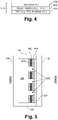
- Fig. 3 is a cross-sectional view showing example "on-glass" components from the Fig. 2 example IGU that enable shutter action, in accordance with certain example embodiments; and Fig. 4 is a cross-sectional view of an example shutter from the Fig. 2 example IGU, in accordance with certain example embodiments.
- Fig. 3 shows a glass substrate 302, which may be used for either or both of the substrates 102 and 104 in Fig. 2 .
- the glass substrate 302 supports on-glass components 304, as well as the shutter 312.
- the conductive coating 404 when unrolled, may be closer to the substrate 302 than the ink layer 406. In other example embodiments, this arrangement may be reversed such that, for example, when unrolled, the conductive coating 404 may be farther from the substrate 302 than the ink layer 406.
- the on-glass components 304 include a transparent conductive coating 306, along with a dielectric material 308, which may be adhered to the substrate 302 via a clear, low-haze adhesive 310 or the like. These materials preferably are substantially transparent.
- the transparent conductive coating 306 is electrically connected via a terminal to a lead to the controller.
- the transparent conductive coating 306 serves as a fixed electrode of a capacitor, and the dielectric material 308 serves as the dielectric of this capacitor.
- the transparent conductive coating 306 may be formed from any suitable material such as, for example, ITO, tin oxide (e.g., Sn02 or other suitable stoichiometry), etc.
- the transparent conductive coating 306 may be 10-500 nm thick in certain example embodiments.
- the dielectric material 308 may be a low dissipation factor polymer in certain example embodiments. Suitable materials include, for example, polypropylene, FEP, PTFE, polyethyleneterephthalate (PET), polyimide (PI), and polyethylenenapthalate (PEN), etc.
- the dielectric material 308 may have a thickness of 4-25 microns in certain example embodiments. The thickness of the dielectric material 308 may be selected so as to balance reliability of the shade with the amount of voltage (e.g., as thinner dielectric layers typically reduce reliability, whereas thicker dielectric layers typically require a high applied voltage for operational purposes).
- low-emissivity (low-E) coatings are conductive.
- a low-E coating may be used in place of the transparent conductive coating 306 in certain example embodiments.
- the low-E coating may be a silver-based low-E coating, e.g., where one, two, three, or more layers comprising Ag may be sandwiched between dielectric layers. In such cases, the need for the adhesive 310 may be reduced or completely eliminated.
- the shutter 312 may include a resilient layer, preferably a polymer material 402.
- a conductive coating 404 may be used on one side of the polymer material 402, and a decorative ink 406 optionally may be applied to the other side.
- the conductive coating 404 may be transparent and, as indicated, the decorative ink 406 is optional.
- the conductive coating 404 and/or the decorative ink 406 may be translucent or otherwise impart coloration or aesthetic features to the shutter 312.
- the polymer material 402 may be formed from a shrinkable polymer such as, for example, PEN, PET, polyphenylene sulfide (PPS), polyether ether ketone (PEEK), etc.
- the polymer material 102 may be 1-25 microns thick in certain example embodiments.
- the conductive coating 404 may be formed from the same or different material as that used for conductive coating 306, in different example embodiments. Metal or metal oxide materials may be used, for example. In certain example embodiments, a 10-50 nm thick material including a layer comprising, for example, ITO, Al, Ni, NiCr, tin oxide, and/or the like, may be used. In certain example embodiments, the resistance of the conductive coating 404 may be in the range of 40-200 ohms/square.
- the decorative ink 406 may include pigments, particles, and/or other materials that selectively reflect and/or absorb desired visible colors and/or infrared radiation.
- the shades 202a and 202b ordinarily are coiled as spiral rolls, with an outer end of the spiral affixed by an adhesive to the substrates 102 and 104 (e.g., or the dielectric thereon).
- the conductive coating 404 may be electrically connected via a terminal to a lead or the like and may serve as a variable electrode of a capacitor having the conductive coating 306 as its fixed electrode and the dielectric 308 as its dielectric.
- variable electrode When an electrical drive is provided between the variable electrode and the fixed electrode, e.g., when an electric drive of voltage or current is applied between the conductive coating 404 of the shutter 312 and the conductive coating 306 on the substrate 302, the shutter 312 is pulled toward the substrate 302 via an electrostatic force created by the potential difference between the two electrodes.
- the pull on the variable electrode causes the coiled shade to roll out.
- the electrostatic force on the variable electrode causes the shutter 312 to be held securely against the fixed electrode of the substrate 302.
- the ink coating layer 406 of the shade selectively reflects or absorbs certain visible colors and/or infrared radiation.
- the rolled-out shade helps control radiation transmission by selectively blocking and/or reflecting certain light or other radiation from passing through the IG unit, and thereby changes the overall function of the IG unit from being transmissive to being partially or selectively transmissive, or even opaque in some instances.
- the electrostatic force on the variable electrode is likewise removed.
- the spring constant present in the polymer material 402 and the conductive coating 404 causes the shade to roll up back to its original, tightly-wound position. Because movement of the shade is controlled by a primarily capacitive circuit, current essentially only flows while the shade is either rolling out or rolling up. As a result, the average power consumption of the shade is extremely low. In this way, several standard AA batteries may be used to operate the shade for years, at least in some instances.
- the substrate 302 may be 3 mm thick clear glass commercially available from the assignee.
- An acrylic-based adhesive having a low haze may be used for adhesive layer 310.
- Sputtered ITO having a resistance of 100-300 ohms/square may be used for the conductive coating 306.
- the polymer film may be a low-haze (e.g., ⁇ 1% haze) PET material that is 12 microns thick.
- a PVC-based ink available from Sun Chemical Inc. applied to 3-8 microns thickness may be used as the decorative ink 406.
- a PEN material commercially available from DuPont that is 6, 12, or 25 microns thick may be used as the polymer material 402.
- evaporated Al that has a nominal thickness of 375 nm may be used.
- sputtered ITO may be used. In both cases, the resistance may be 100-400 ohms/square.
- the ITO or other conductive material(s) may be sputtered onto, or otherwise formed on, their respective polymer carrier layers in certain example embodiments.
- these example materials, thicknesses, electrical properties, and their various combinations and sub-combinations, etc. should not be deemed limiting unless specifically claimed.
- Certain example embodiments may include microscopic perforations or through-holes that allow light to pass through the shade and provide progressive amounts of solar transmittance based on the angle of the sun. These perforations or holes may help shade the direct sun, progressively. The shading effects of the microscopic holes can be compared to that of exterior blinds, except that the holes remain invisible, as they are formed to be too small for the human eye to see, in certain example embodiments.
- the holes' size, distribution, and angle may be designed to control the amount solar energy allowed into the building during different times of the year. For instance, in the summer, where the sun is high in the sky, the holes' size, distribution, and angle may help ensure that solar transmittance from the sunlight is reduced while still allowing some light into the building.
- the holes may be designed such that the shade allows solar transmittance in the winter, which reduces the need for heating during the cold period.
- through hole design it may be possible to reduce the amount of energy from sunlight passing through the IG unit by up to about 90% in the summer (and sometimes even more), while also allowing for about 35% of solar transmittance in the winter (and sometimes even more).
- the perforations thus may be used to provide a passive approach to solar control in connection with the more active and dynamic use of the electrostatically driven shade.
- hole design may enable a reduction in the amount of energy from sunlight passing through the IG unit in the summer of at least 50%, more preferably at least 60%, still more preferably at least 75%, and sometimes 80-90% or more.
- hole design may enable transmission of energy from sunlight passing through the IG unit in the winter of at least 20%, more preferably at least 25%, and sometimes 30-35% or more.
- a single hole design may enable a difference in transmission of energy from sunlight passing through the IG unit between the summer and winter of at least about 30%, more preferably at least about 40%, and still more preferably at least about 50-55% and sometimes even more.
- the size, shape, and/or arrangement of the holes may be based on, for example, the approximate latitude at which the IGU is to be installed, the orientation of the IGU in the location (e.g., whether the IGU is upright as for a door or window, flat or angled as for a skylight, etc.), etc.
- Different angles for the holes may, for example, be tuned in these and/or other regards, e.g., to provide for improved shading coefficients, light-to-solar gain values, etc.
- thickness (T) of the dynamic shade may be 10-32 um in certain example embodiments.
- the size of the hole diameter or major distance (D) may depend on that thickness in some instances.
- the hole diameter or major distance in certain example embodiments may be between 0.5T and 5T.
- 0.5T equates to direct sunlight not passing through the film at an angle of greater than 26.5 degrees to the horizon. This assumes that the hole angle is perpendicular to the outboard face of the dynamic shade. The amount of light is dependent on the diameter of the hole, the thickness of the dynamic shade, the angle of the holes and the number of holes.
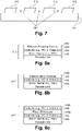
- Fig. 5 is a cross-sectional, schematic view of an example IGU incorporating an electric potentially-driven shade including perforations 502, which may be used in connection with certain example embodiments.
- the holes are formed in the shutter 312 portion of the shade. That is, the holes 502 extend through the decorative ink 406, polymer material 402, and the transparent conductive coating 404 thereon.
- the holes 502 need not, however, extend through the lower on-glass portion 304 of the shade in certain example embodiments. This may be advantageous from a manufacturing perspective, as the on-glass portion 304 may be formed separately from the shutter 312 portion, in some instances.
- the on-glass portion 304 may use blanket coating processes such as sputtering or the like, whereas the shutter 312 portion may include additional steps practiced after the polymer material 402 is coated with the transparent conductive coating 404 and/or ink 406.
- the holes 502 in the shutter 312 portion may be formed by any suitable technique.
- micro-holes may be formed by laser cutting, stamping, punch-cutting, a photolithographic approach, a drilling approach (such as, for example, physical drilling, electron beam drilling, etc.), and/or the like.
- the holes may be formed to have a cross-section that is substantially circular, rectangular, etc.
- the hole diameter or major distance will be approximately the thickness of the entire shade and, thus, approximately 10-30 microns.
- the holes modify the color rendering index (CRI) value of the overall shade preferably by no more than 10, more preferably by no more than 5, still more preferably by no more than 2-3, and sometimes by no more than 1 (e.g., by no more than 0.5).
- CRI color rendering index
- the holes may be formed by providing multiple lamellas stacked one on top of another.
- holes in adjacent lamella layers may or may not partially or fully overlap with one another.
- multiple lamella layers may fully overlap with one another to in essence form a through hole in one example
- another example may involve adjacent lamella layers may only partially overlap with one another to in essence form an angled through hole.
- multiple lamella layers may not overlap with one another.
- multiple lamellas may be stacked up to form (or in essence take the place of a separate) shutter 312.
- Figs. 6a-6b demonstrate how solar radiation can be selectively reflected in connection with the Fig. 5 example IGU, in certain example instances.
- Fig. 6a for example, when the sun 600 is high (e.g., in summer months), solar radiation 602a is more likely to encounter a non-removed portion of the shutter 312 of the extended shade, as compared to the holes 502 formed therein. Thus, a substantial amount of solar radiation is reflected 602b (and/or absorbed, depending on the example embodiment).
- solar radiation 602c is more likely to pass through the holes 502 formed in the shutter 312 portion of the shade.
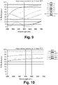
- Fig. 7 is a cross-sectional view showing an alternative geometry for the perforations formed in the Fig. 5 example shade, in accordance with certain example embodiments.
- the holes formed in the shutter 312 portion of the shade may be angled.
- Fig. 7 shows the holes 502' formed in the shutter 312 being angled. This may aid in selective transmission through the shade in certain example embodiments.
- the dynamic shade mechanism uses a coiled polymer with a conductive coating.
- the conductive coating 404 may be formed to be integral with the polymer material 402, or it may be an extrinsic coating that is applied, deposited, or otherwise formed on the polymer material 402.
- decorative ink 406 may be used together with a transparent conductive coating material (e.g., based on ITO) and/or an only partially transparent or opaque conductive coating.
- An opaque or only partially transparent conductive coating may obviate the need for ink in certain example embodiments.
- a metal or substantially metallic material may be used in certain example embodiments.
- Aluminum is one example material that may be used with or without a decorative ink.
- the use of aluminum may be seen to be advantageous in some instances because it provides excellent conductivity (low resistivity) and high levels of reflectivity with respect to incident light from the sun, both in the visible and infrared spectra.
- a metal or substantially metallic layer such as a layer comprising or consisting essentially of aluminum
- the internal reflection (and particularly the specular reflection) from it may be aesthetically unpleasing.
- the inclusion of the layer may result in a displeasing coloration for a viewer on the interior-facing side of the IGU.
- Antireflection (AR) techniques are known and are used in connection with certain coated articles. Typically, a layer or series of layers can be deposited on top of the surface whose reflection is to be reduced. Such techniques oftentimes use an optical interference model, e.g., where high and low index of refraction materials are provided over the surface whose reflection is to be reduced, typically in an alternating manner. Unfortunately, however, reducing the reflection of a "very shiny" metal such as that resulting from an aluminum, chrome, molybdenum, or otherwise coated surface presents heightened technical challenges. Reducing the reflection of the surface of uncoated glass from about 10% to about 1%, for example, can be complicated but can nonetheless be accomplished using the optical interference technique described above.
- Figs. 8a-8c are cross-sectional views of shutters similar to the Fig. 3 example, except that overcoats are included to improve the aesthetic appearance of the overall shade, in accordance with certain example embodiments.
- the shutter 312' of Fig. 8a includes a reflection-reducing overcoat 802, whereas the shutter 312" of Fig. 8b includes a dielectric mirror overcoat 804. As shown in Figs.
- the reflection-reducing overcoat 802 and the dielectric mirror overcoat 804 are provided over a conductive coating 404 and on a major surface of the polymer material 402 comprising (for example) PEN opposite decorative ink 406. It will be appreciated, however, that the ink 406 need not be provided, e.g., if the conductive coating 404 is not transparent. Mirror coatings such as, for example, Al, may obviate the need for decorative ink 406. It also will be appreciated that the reflection-reducing overcoat 802 and the dielectric mirror overcoat 804 may be provided on major surfaces of the shade-polymer material 402 comprising (for example) PEN opposite the conductive coating 404 in certain example embodiments.
- a variety of materials may be used for the reflection-reducing overcoat 802 and the dielectric mirror overcoat 804.
- Single layers that may be used for the reflection-reducing overcoat 802 may include, for example, layers comprising or consisting essentially of Ni, Cr, NiCr, NiCrOx, Inconel, amorphous silicon (a-Si), arc carbon, tetrahedral amorphous Carbon (Ta-C), Sb, Ti, NiTi, NiTiOx, and/or the like.
- such layers may be formed to a thickness of 5-100 nm, more preferably 5-60 nm, still more preferably 10-60 nm, and sometimes 20-50 nm or 30-50 nm. More specific examples will be provided below.
- a layer stack comprising a layer of Al sandwiched between layers comprising an oxide of Ni, Ti, and/or Cr (e.g., layers comprising NiCrOx) may be used in certain example embodiments.
- Fig. 8c is a shutter similar to Fig. 3 , except that a phase shifter layer 806 in essence "splits" the conductive coating, in accordance with certain example embodiments.
- first and second conductive coatings 404a and 404b sandwich a phase shifter layer 806 in forming shutter 312"'.
- the same or similar materials and/or material thicknesses as those mentioned above in connection with the Figs. 8a-8b examples may be used in connection with the Fig. 8c example.
- the first and second conductive coatings 404a and 404b may comprise or consist essentially of a metal such as Al or Ni, NiCr, tin oxide, ITO, and/or the like.
- the phase shifter layer 806 may comprise or consist essentially of Ni, Cr, and/or Ti or an oxide of thereof. Titanium nitride and titanium oxynitride also may be used in connection with the phase shifter layer 806.
- the phase shifter layer 806 works in connection with the first and second conductive coatings 404a and 404b and may be thought of as a reflection-reducing layer. More particularly, having a phase shifter between one completely reflecting and one partially reflecting layer advantageously creates two identical intensities of the light and simply phase shifts them to obtain an at least partial cancellation effect. It will be appreciated that the lower conductive coating 404a may be conductive in certain example embodiments.
- the stack including the phase shifter layer 806 and the conductive coatings 404a and 404b may be conductive.
- different levels of reflectivity may be provided for the first and second conductive coatings 404a and 404b, although this need not necessarily be the case in all example embodiments.
- the level of reflectivity may be tuned based on the thickness of the coatings (e.g., thicker coatings tend to be more reflective).
- the first conductive coating 404a may be thinner and/or less reflective than the second conductive coating 404b, e.g., so as to permit light to be absorbed by the decorative ink 406. This arrangement may be reversed in certain example embodiments.
- spectral reflection also can be adjusted by reducing total reflection and/or moving the layer from a specular reflective material to a diffuse reflecting material.
- the following techniques may be used in this regard, and may be used in any suitable combination, sub-combination, or combination of sub-combinations with each other and with the Fig. 8a-8c approaches.
- a first technique involves roughening the upper surface of the conductive (oftentimes metallic) coating by sand, bead, grit, or other blasting, through laser ablation, imprinting using a stamp or the like, etc. This may help to increase the surface roughness of the conductive coating and create a desired diffuse reflective effect.
- the surface roughness (Ra) is less than 3.2 ⁇ m.
- Another approach that may be used involves chemical (e.g., acid) etching of the conductive coating that adds pits and therefore increases the surface roughness.
- Still another approach involves imprinting the polymer substrate with various patterns, prior to coating the material with the conductive coating. Doing so may help increase the surface roughness of the polymer substrate and, with a generally conformal thin film formation process such as sputtering or the like, the texture of the polymer substrate can in effect be transferred to the conductive coating. This can be accomplished during a calendaring process, e.g., where the rolls that the polymer film go through have a pattern that is transferred to the polymer substrate.
- the first and/or second major surfaces of the polymer substrate may be patterned to have a texture in a predefined pattern, e.g., with that pattern being defined at least in part in terms of textural features to be imparted to the polymer material.
- the depth of the features may be predefined.
- the predefined pattern may be defined at least in part with respect to the area extending across the polymer substrate.
- a fractal pattern may be used. It will be appreciated that stamping, punching, and/or the like may be used in addition to, or in place of, the calendaring.
- a metallic layer such as aluminum
- it may be anodized.
- the anodizing of the metallic layer may help roughen the surface and add color, as well, which may be advantageous in certain example embodiments.
- Still another approach involves applying an ink directly or indirectly to the surface of the conductive coating.
- the ink may or may not be continuous.
- a PVC-based ink is applied to the polymer substrate on the side opposite the conductive coating.
- putting an ink on the conductive coating would help lower reflection and create another avenue for adding different colors, images, and/or the like, to the shutter.
- the ink here may be used in place of, or together with, the ink on the opposite side of the polymer substrate.
- a textured surface to the base polymer, modifying the conductive coating chemically or physically, and/or add an ink layer, e.g., to accomplish the same or similar ends, achieve further reductions in unwanted reflection, etc.
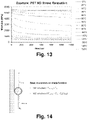
- Figs. 9-11 are graphs plotting percent reflectance vs. wavelength for certain example overcoat materials that may be used in connection with the Fig. 8a-8b layer stacks, in certain example embodiments. The data shown in these graphs are modelled.
- Each of Figs. 9-11 shows the reflection of bare aluminum on a 12 micron thick PET sheet, as a function of wavelength. The aluminum may be deposited via an evaporative technique, electrochemical deposition, and/or the like.
- These graphs also show the reflection of a layer stack including the same aluminum layer overcoated with a single layer coating of various materials (with the exception of the overcoated NiCrOx/Al/NiCrOx layer stack).
- the thickness of these layers has been selected to achieve as low a reflection as possible, while at the same time minimizing the reflected color change.
- low-reflectivity and pan-chromaticism are difficult to achieve simultaneously.
- the best curve is achieved with arc carbon, a material which is not sputtered but instead may be formed by striking an arc by passing large currents through a pure carbon rod that is pressed against a carbon plate.
- this material is desirable from reflectivity and chromaticism perspectives, it may not be feasible for large-scale production.
- Ta-C approximates the performance of arc carbon, and Ta-C can be sputtered using, for example, a graphite target. A layer comprising Ta-C therefore may be desirable in certain example embodiments. Further findings concerning overcoat materials are presented below.
- An overcoat layer comprising NiCrOx was formed on a layer comprising Al, reducing reflection as shown in Figs. 9 and 11 .
- Thicknesses for the overcoat layer comprising NiCrOx ranged generally from 20-60 nm, with specific examples including 20 nm, 30 nm, 40 nm, 45 nm, 47 nm, 49 nm, 50 nm, and 57 nm.
- an 80Ni-20Cr target may be used, and this target was assumed for purposes of the simulations shown in Figs. 9 and 11 .
- the oxygen content can be modified to produce a varying array of colors, while still being conductive.
- a 50-60nm thick sample film was formed over a layer comprising Al, and the color of the film was a blue-purple color, which shows good agreement with the models. In this case is used. Alternate stoichiometry of NiCr may produce different results in different example embodiments.
- NiCrOx and Al can be applied on the shade. That is, a layer comprising Al was sandwiched between layers comprising NiCrOx, and this three-layer stack was applied over the conductive coating comprising Al. Modeling was completed to optimize the layers to produce a low reflectance top coat surface. The results of the model can be seen in Fig. 9 . The total reflectance was less than 15%. In this case, 80Ni-20Cr was used, although alternate stoichiometry for the NiCr may produce different results. As above, the oxygen content can be modified to produce a varying array of colors, while still being conductive.
- a layer stack comprising NiCrOx/Al/NiCrOx may have a total thickness of 3-60 nm, more preferably 3-30 nm, and still more preferably 3-15 nm.
- monolayers comprising NiCrOx, Al, or the like may be 3-15 nm thick.
- Another method to significantly reduce the total visible light reflectance of the aluminum layer involves the addition of a carbon overcoat.
- the application of carbon via cathodic arc deposition was modelled to determine the reduction of visible light reflection and can be seen in Figs. 9 and 11 .
- the optimized model predicts a total reflectance of less than 10%.
- Example thicknesses are in the range of 30-60 nm, with specific examples of 45 nm and 50 nm.
- a layer comprising metallic NiCr also can be deposited over the conductive coating comprising Al to reduce the total visible light reflection.
- Fig. 10 shows the modelled performance of layers that are 10 nm thick, 20 nm thick, 30 nm thick, and 40 nm thick.
- Fig. 11 shows an example that is 43 nm thick, and 45 nm and 47 nm thick samples also are specifically contemplated.
- a-Si e.g., 20-30 nm thick and, for example, 21 nm thick, 23 nm thick as shown in Fig. 11 , and 25 nm thick
- Inconel such as, for example, Inconel 600 (e.g., 40-60 nm thick and, for example, 47 nm thick, 50 nm thick as shown in Fig. 11 , and 53 nm thick)
- Ta-C e.g., 20-60 nm thick, with specific examples being 39 nm thick, 41 nm thick, 43 nm thick, 45 nm thick as shown in Fig. 11 , 47 nm thick, and 49 nm thick).
- Inconel is a family of austenitic nickel-chromium-based super-alloys that are oxidation-corrosion-resistant materials.
- Inconel 600 includes (by mass) 72.0% Ni, 14.0-17.0% Cr, 6.0-10.0% Fe, 1.0% Mn, 0.5% Cu, 0.5% Si, 0.15% C, and 0.015% S.
- internal reflection preferably is reduced to less than 60% over all or substantially all of a wavelength range of 400-700 nm, more preferably less than 50% over all or substantially all of a wavelength range of 400-700 nm, and still more preferably less than 30-40% over all or substantially all of a wavelength range of 400-700 nm.
- internal reflection is reduced to less than 20% over all or substantially all of a wavelength range of 400-700 nm (e.g., as may be the case with a carbon-based overcoat).
- the amount of reflection varies by no more than 30% points over all or substantially all of a wavelength range of 400-700 nm, more preferably by no more than 20% points over all or substantially all of a wavelength range of 400-700 nm, and sometimes by no more than 10-15% points over all or substantially all of a wavelength range of 400-700 nm.
- An oxygen plasma and/or other cleaning process may be used on the polymer material 402, e.g., prior to formation of the conductive coating 404, in certain example embodiments.
- the materials may be selected, and that the overall layer stack formed, to have mechanical and/or other properties that facilitate the same.
- an excess of stress in a thin film layer stack typically is seen as disadvantageous.
- excess stress can lead to cracking, "delamination” / removal, and/or other damage to the conductive coating 404 and/or an overcoat layer or layers formed thereon.
- low stress and in particular low tensile stress
- the adhesion of sputtered thin films depends on, among other things, the stress in the depositing film.
- One way stress can be adjusted is with deposition pressure. Stress versus sputter pressure does not follow a monotonic curve but instead inflects at a transition pressure that in essence is unique for each material and is a function of the ratio of the material's melting temperature to the substrate temperature. Stress engineering can be accomplished via gas pressure optimizations, bearing these guideposts in mind.
- temperatures internal to an IG unit may become quite elevated.
- an IG unit in accordance with the Fig. 2 example and including a black pigment may reach a temperature of 87 degrees C, e.g., if the black portion of the shade is facing the sun in elevated temperature, high solar radiation climates (such as, for example, in areas of the southwest United States such as Arizona).
- the performance of the material's otherwise advantageous mechanical properties may degrade overtime, especially with elevated temperature exposure. If these mechanical properties degrade significantly, the shade may no longer function (e.g., the shade will not retract).
- Figs. 12-13 help demonstrate these points. More particularly, Fig. 12 demonstrates the effect of temperature on Young's modulus in that it is a graph plotting Young's modulus vs. temperatures for different polymer materials, and Fig. 13 is shows typical stress relaxation curves for a PET film at different temperatures. In Fig. 12 , film A is PEN, film B is PET, and film C is PI. In general, polymers materials with higher glass transition temperatures have improved elevated temperature mechanical properties.
- PEN polyimide
- PI Polyimide
- Tg Tg of ⁇ 142 degrees C
- Kapton HN Tg of ⁇ 380 degrees C. Both of these materials have better mechanical properties in elevated temperature environments, compared to PEN. This is especially true at temperature above 100 degrees C.
- the following chart demonstrates this, referencing mechanical properties of PEN (Teonex), PEEK, and PI (Kapton HN).
- UTS stands for ultimate tensile strength, in the chart.
- the modification of the shade base material from its current material (PEN) to an alternate polymer (e.g., PEEK or PI/Kapton) that has increased elevated temperature mechanical properties may be advantageous in certain example embodiments in the sense that it may enable the shade to better withstand internal IG temperatures, especially if the shade is installed in higher temperature climates. It will be appreciated that the use of an alternative polymer may be used in connection with the shutter and/or the on-glass layer in certain example embodiments.
- PEN current material
- an alternate polymer e.g., PEEK or PI/Kapton
- certain example embodiments may use a dyed polymer material.
- a dyed PEN, PEEK, PI/Kapton, or other polymer may be used to created shades with an assortment of colors and/or aesthetics.
- dyed polymers may be advantageous for embodiments in transparent/translucent applications, e.g., where the shade conductive layer is a transparent conductive coating or the like.
- PI/Kapton is a known polymer that has been used in a variety of applications, it sometimes is seen as unacceptable in applications where optics and aesthetics are important. This includes many window applications.
- One reason for the limited adoption of PI/Kapton relates to the conventional thought that it has a generally yellow-orange coloration. This coloration typically seen as aesthetically unpleasing.
- PI/Kapton can be easily avoided. Nevertheless, it would be desirable to use PI/Kapton (and/or PEN) for the shade in certain example embodiments, as it can withstand high temperatures and possesses good mechanical properties, even at high temperatures, e.g., as outlined above.
- PI/Kapton and/or PEN also have good shrinkage characteristics (e.g., controllable and high shrinkage rates, ability to form strong coils, etc.), thereby providing for a good spring for the shutter.
- good shrinkage characteristics e.g., controllable and high shrinkage rates, ability to form strong coils, etc.
- PI/Kapton it would be counterintuitive to use PI/Kapton for the shutter.
- the inventors have, however, recognized that in example embodiments where the shutter is opaque or substantially opaque, the coloration of the PI/Kapton becomes rather unimportant. That is, when PI/Kapton is used in connection with an opaque or only partially transparent shutter, its yellow-orange coloration is not easily perceivable with the naked eye.
- PI/Kapton may be applied as a liquid (e.g., over ITO or another conductive coating) and cured, thereby allowing for rapid, low-cost and high-volume manufacturing over potentially large areas, suitable for windows.
- PI/Kapton has a better high temperature modulus and high temperature yield strength, better elevated temperature stress relaxation resistance, higher glass transition temperature, etc., compared to alternative shutter materials.
- PI/Kapton also may now come in different colors (e.g., related to dying) such as, for example, black.
- a transparent or translucent shades may be desirable for some applications. Shades of these types can be created using the base polymer (e.g., PEN) together with a conductive layer of a transparent conductive coating such as ITO or a low-E type coating that creates a color shift.
- the base polymer e.g., PEN
- a conductive layer of a transparent conductive coating such as ITO or a low-E type coating that creates a color shift.
- a dyed base polymer e.g., PEN, PEEK, PI/Kapton
- the dying may be accomplished by impregnating dyestuffs, UV absorbers, and/or the like throughout the matrix of the film substrate.
- the conductive coating on shutter serves several purposes including, for example, receiving voltage to make the shade go up and down.
- the conductive coating on the shutter may be highly reflective in the IR and/or UV spectra.
- the transparent conductive coating also increases the coil spring force of the shade, e.g., as a result of its mechanical properties (include modulus of elasticity and yield strength).
- the coil force also is increased via the transparent conductive coating as a result of the thermal expansion mismatch between the conductive coating material and the polymer substrate during the heat treating process used to manufacturer a coil.
- the polymer substrate e.g., PI, PEN, or the like
- Tg glass transition temperature
- the irreversible shrinkage pf the polymer causes a residual stress mismatch between the polymer substrate and conductive layer that creates a coiled spring.
- the CTE difference is good for coil force but bad for cracking/crazing/delamination/etc. This is one reason why a metal conductive layer or a conductive coating comprising a metal conductive layer as described herein may perform better than the ITO layer. That is, the ITO is intrinsically brittle and cracks extensively upon high stresses, resulting in the loss of the capability to sustain the stress needed for spring force development.
- the strength of the coiled spring depends on the material that is being used as the conductive layer, as well as the thickness of the conductive layer.
- the conductive layer found on the polymer may comprise Al, a combination of Al and Cr, ITO, and/or the like.
- Al-inclusive conductive layers may be beneficial in opaque applications, whereas ITO-inclusive conductive layers may be better suited for transparent/translucent applications.
- Al thickness of about -375 nm and given the low modulus of elasticity of Al, a coil with this composition may be limited in the extent to which it can function (e.g., the height of the IG unit or length of the shade may be limited).
- a longer coil will have more mass and, if the spring force is not greater the weight of the coil in the extended condition, the shade will not retract (roll up).
- a spring force range that a coil must have in order to be a working shade. For instance, if the spring force of the coil is less than the weight of the coil, then the coil will not retract (and the shade will always be in the down position). Similarly, if the coil spring force is greater than the sum of the weight of the coil and the maximum electrostatic force that can be applied (with the electrostatic force being a function of the voltage applied and the dielectric layer's thickness and its dielectric constant), the coil will not extend (go down).
- Fig. 14 summarizes the basic constraints on the shade function that may come into play in certain example embodiments.
- Certain example embodiments relate to alternate conductive materials that beneficially modify the spring force of the coiled shade to make it usable for various lengths.
- the inventors have recognized that properties of the conductive layer that increase the strength of the coil include an increase in the elastic modulus, an increase in the difference in coefficient of thermal expansion (CTE) between the polymer substrate and the conductive layer, and an increase in the elastic modulus to density ratio.
- Some of the pure metals that can be used to increase coil strength compared to Al or Cr include Ni, W, Mo, Ti, and Ta.
- the elastic modulus of studied metal layers ranged from 70 GPa for Al to 330 GPa for Mo.
- the CTE of studied metal layers ranged from 23.5 x 10 -6 /k for Al down to 4.8 x 10 -6 /k for Mo.
- incorporating Mo and Ti based conductive layers into shades has resulted in a spring force of the coil that is significantly higher than that which is achievable with Al.
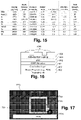
- the Fig. 15 table includes coil strength related properties for several materials, which may be relevant in certain example embodiments.
- Certain example embodiments advantageously include a polymer substrate based on PEN, PEEK, PI, or the like, supporting (in order moving away from the substrate) a layer comprising Al followed by a layer comprising Mo. Certain example embodiments advantageously include thin film layer(s) in a conductive coating and/or a conductive coating itself with a greater modulus and lower CTE than Al.
- certain example embodiments may incorporate a thin overcoat layer comprising Al, Ti, stainless steel, or the like, e.g., to increase corrosion resistance.
- a protective oxide e.g., aluminum oxide, titanium oxide, or chromium oxide for SS
- the oxide in general will form to be about 2-7 nm thick. At least 5 nm of the base metal is needed to provide some protection, and certain example embodiments may include about 50 nm or more of the base material, as the additional thickness can help increase the coil strength.
- the thin layer comprising Al may be used to shift the stress regime of the layer stack supported by the polymer substrate from a net tensile stress regime to a net compressive stress regime. It is noted that there is a balance, however, in terms of moving from a regime that could promote cracking to a regime that if taken too far can produce wrinkling. Thus, it will be appreciated that certain example embodiments can improve spring performance through the use of alternate materials, with or without stress-ameliorating underlayers.
- the thickness of the stress-reducing layer may vary based on how much stress is to be alleviated, and other materials may be used in different example embodiments.
- the reflectivity may not be as high as it otherwise would be and/or the coloration may not be shifted too far in a disadvantageous range, even for transparent type applications.
- the thickness of the underlayer and/or the corrosion-reducing overcoat individually or collectively, may be less than 375 nm. It will be appreciated that thin film layer(s) in the second conductive coating may be selected and formed to cause the shutter to move between the opened and closed positions with a spring force greater than that of a shutter having a second conductive coating including only a layer comprising Al.
- a PEN, PI, or other polymer substrate used as a shutter may support a thin layer comprising Al for stress-engineering purposes, with a conductive layer comprising Mo, Ti, or the like directly or indirectly thereon.
- the conductive layer may support a corrosion-resistant layer comprising Al, Ti, stainless steel, or the like.
- the side of the substrate opposite these layers optionally may support a decorative ink or the like.
- Certain example embodiments may incorporate solar cells into the IG unit design and, thus, relate to BIPV technology. For instance, certain example embodiments incorporate solar cells into the shutter. In this way, solar energy is not "wasted.” A variety of different solar technologies are available. However, certain example embodiments take advantage of copper indium gallium selenide (CIGS) type solar cells, as they typically are the most flexible type of solar cells available. A CIGS solar cell is a thin-film solar cell used to convert sunlight into electric power.
- CIGS copper indium gallium selenide
- a CIGS solar cell may be manufactured by depositing a thin layer of copper, indium, gallium, and selenide on glass or plastic backing, along with electrodes on the front and back to collect current. Because the material has a high absorption coefficient and strongly absorbs sunlight, a much thinner film is required than of other semiconductor materials. This in turn imparts the potential for high flexibility noted above.
- Certain example embodiments use the conductive (e.g., metallic) layer on the coil as the base conductive layer of the CIGS module.
- a thin n-type buffer layer is added on top of the absorber.
- the buffer layer on the conductive layer is typically cadmium sulfide (CdS) deposited via chemical bath deposition or the like.
- the buffer is overlaid with a thin, intrinsic zinc oxide layer (i-ZnO), which is capped by a thicker, aluminum-doped zinc oxide layer (ZnO:Al or AZO).
- i-ZnO intrinsic zinc oxide layer
- ZnO:Al or AZO thicker, aluminum-doped zinc oxide layer
- the i-ZnO layer is used to protect the CdS and the absorber layer from sputtering damage while depositing the ZnO:Al layer, as the latter is usually deposited by DC sputtering, which is known to be a process likely to damage sensitive materials.
- the salinization process is known to use high temperatures, as well. Thus, using PI, PEN, and the like, are good options for the shutter, e.g., as they are able to handle the higher temperatures, as discussed above.
- the AZO layer serves as a transparent conducting oxide to collect and move electrons out of the cell while absorbing as little light as possible. Further details regarding CIGS technology, including techniques for creating CIGS solar cells, materials and material thicknesses that may be used, etc., may be found in U.S. Patent Nos. 9,691,917 ; 9,419,151 ; 9,312,417 ; 9,246,025 ; 8,809,674 ; and 8,415,194 ,
- the shade could act as a CIGS photovoltaic module.
- the power generated from the CIGS shade could be used to power rechargeable batteries that are used in the function of the shade or be contacted to the home/office. This may be particularly advantageous in retrofit applications, e.g., where it may be difficult or impossible to connect the shade to an external power supply.
- the unit of certain example embodiments may be self-sufficient in terms of power by virtue of the inclusion of the CIGS solar cell.
- Fig. 16 is a schematic view of a shutter incorporating a CIGS solar cell that may be used in connection with certain example embodiments.
- the shade polymer substrate 406 supports a conductive coating 404 on one major surface, and an optional decorative ink on the opposite major surface.
- Other layers involved in functionality of CIGS solar cell are formed on the conductive coating 404 and include, for example, the CIGS absorber layer 404, another conductive layer 1604 (e.g., of or including ZnO).
- An optional antireflection coating 1606 is formed on the upper conductive layer 1604. This antireflection coating 1606 may help increase the amount of visible light reaching the CIGS absorber layer 404 in certain example embodiments.
- the AR coating 1606 may be a single, broadband AR layer in certain example embodiments. In other example embodiments, the AR coating 1606 may include multiple layers that act on the optical interference principle noted above and, thus, may include alternating high and low index of refraction dielectric material layers. The AR coating 1606 also may aid in coloration of the shutter, as above. Front contact 1608 also is provided.
- the conductive coating 404 in certain example embodiments may be a multilayer coating. In such cases, the conductive coating may include a layer or layers comprising Mo, Al, Cr, Ni, Y, and/or the like. For instance, in certain example embodiments, a thin layer comprising Al may support a layer comprising Mo.
- This arrangement may be advantageous in that the inclusion of the Mo-inclusive layer may serve as an efficient back contact for the CIGS absorber layer 1602, while also improving the operation of the spring associated with the shutter, while the inclusion of the Al-inclusive layer may aid in maintaining the conductivity of the Mo back contact while also advantageously impacting the stress regime in the overlying CIGS-related layers (including the layer comprising Mo).
- the already flexible CIGS materials may be manufactured to be yet more appropriate for shutter-related applications, in certain example embodiments.
- a layer comprising Mo that is 0.5-5 ⁇ m thick a CIGS-inclusive layer that is 1-7 ⁇ m thick, a CdS-inclusive layer that is 0.01-0.1 ⁇ m thick, a layer comprising ZnO that is 0.1-1 ⁇ m thick, and an AR coating that is 0.05-0.15 ⁇ m thick.
- FIGs. 17-19 show how the shade may be connected to a glazing and powered, in accordance with certain example embodiments.
- the on-glass components of the shade 1702 are attached to a hollow anchor stop 1704 or bus bar and the substrate 1706 via a silver paste 1708 and epoxy 1710 or the like. Wires are soldered to the anchor stop 1704 and then run around the perimeter to the bottom of the IG unit, where the bottom anchor stop (locking restraint) is located.
- An electrical connection is created between the ITO or other conductive coating 306 on the substrate 302 and conductive tapes 1802 and 1804 (such as, for example, copper tape) via a conductive epoxy, Anisotropic Conductive Film (ACF), or the like 1806.
- Wires are soldered to the conductive tape 1802 and 1804 and run along the perimeter of the IG unit to a bottom corner where two wires (ITO substrate wire and anchor stop wire) protrude through the IG spacer to the outside of the IG unit, e.g., for electrical connection to an external power source or the like.
- Fig. 20 is a schematic diagram showing an alternative approach for how the shade may be connected to the glazing and powered, in accordance with certain example embodiments.
- This example alternate design includes printing or otherwise applying silver frit 2002a-2002b on the glass substrate 2000, e.g., around its peripheral edges.
- the on-glass components 304 e.g., including the PET or other polymer film 308 and the TCC 306 comprising ITO or the like
- the on-glass components 304 are laminated on top of the Ag frit 2002a-2002b.
- a first portion of the Ag frit 2002a on the glass 2002 is bonded or otherwise electrically connected to the TCC 306 comprising ITO or the like via a conductive epoxy, ACF, or the like, thereby forming an Ag frit to ITO layer connection 2012.
- upper bus bar 2004, and lower bus bar 2006 are secured on top of the on-glass components 304 with epoxy or the like.
- Wires 2008a and 2008b are soldered from the upper and lower bus bars 2004 and 2006 to a second portion of the Ag frit 2002b as shown in Fig. 20 , and from the lower bus bar 2006 and the first portion of the Ag Frit 2002a.
- the wires 2014a and 2014b from the first portion of the Ag Frit 2002a and the lower bus bar 2006 protrude through the IG spacer to the outside of the IG.
- These protruding wires may be connected to a power source and/or controller.
- One or more seals may be provided to help restrict outgassing from the cavity of the IG unit, ingress of moisture into the cavity of the IG unit, etc.
- Fig. 21 is a schematic diagram showing an alternative approach for how the shade may be connected to the glazing and powered, in accordance with certain example embodiments.
- This example alternate design includes the use of Ag frit, but lacks wires, at least internal to the spacer.
- the on-glass components 304 are laminated on top of the Ag frit 2002a-2002b.
- a first portion of the frit 2002a is bonded or otherwise electrically connected to the TCC 306 comprising ITO or the like via a conductive epoxy, ACF, or the like.
- the shade, upper bus bar 2004, and lower bus bar 2006 are secured on top of the glass 2000' with epoxy or the like and to the Ag frit via brazing, soldering, and/or the like.
- bus bar to Ag frit connections 2100a-2100b shown in Fig. 21 .
- These bus bar to Ag frit connections 2100a-2100b are provided with respect to the second portion of Ag frit 2002b and take the place of the wires 2008a-2008b.
- Electrical connections to the edge of the glass occur via Ag frit 2102 that goes under the spacer.
- This Ag frit 2102 extends from the lower bus bar 2006 and an end of the first portion of Ag frit 2002a that is closer to the lower bus bar 2006, thereby taking the place of the wires 2014a-2014b in the Fig.
- brazing, soldering, conductive epoxy, ACF, and/or the like may be used to form these electrical connections.
- Electrical wire connectors can be soldered to the Ag frit on the outside of the IG, or at least external to the spacer.
- the lack of a hole may reduce the likelihood, or slow the progress, of gas leaks, moisture ingress into the IG unit's cavity, etc.
- These problems might otherwise reduce the lifetime of the IG unit, e.g., by reducing the likelihood of internal moisture from occurring.
- the presence of internal moisture can create unwanted haze and at even 5-8% relative humidity can cause unwanted charging and premature shade failure.
- Ag frit is mentioned, it will be appreciated that other types of frit may be used in different example embodiments. It also will be appreciated that having a low-E coating, ITO, or other conductive material directly on the glass (e.g., without a laminating layer) may be used to serve the same or similar purpose as the Ag frit.
- first and second electrically conductive bus bars may be located at first and second opposing edges of the first substrate, with each of the bus bars having first and second ends, and with the first and second bus bars being provided, directly or indirectly, on the dielectric or insulator film.
- First and second patterns of conductive frit may be applied, directly or indirectly, to the first substrate, the frit being interposed between the first substrate and the first conductive coating, with the first pattern of frit electrically connecting with the first conductive coating, with the first and second pattern extending along third and fourth opposing edges of the first substrate, with the first through fourth edges being different from one another, and with the first pattern extending in a direction from the first end of the first bus bar towards the first end of the second bus bar, the second pattern extending in a direction from the second end of the first bus bar towards the second end of the second bus bar.
- a conductive epoxy, anisotropic conductive film (ACF), or the like may electrically connect the first pattern of frit with the first conductive coating.
- a first set of wires may electrically connect the first and second bus bars to the second pattern of frit proximate to the second ends thereof; and a second set of wires may electrically connect to the first end of the second bus bar and an end of the first pattern of frit proximate to the first end of the second bus bar.
- the second set of wires may protrude through a hole in the spacer system for electrical connection to the power source.
- third and fourth patterns of conductive frit may electrically connect the first and second bus bars to the second pattern of frit proximate to the second ends of the first and second bus bars; and fifth and sixth patterns of conductive frit may electrically connect to the first end of the second bus bar and an end of the first pattern of frit proximate to the first end of the second bus bar.
- the fifth and sixth patterns of frit may extend towards outer edges of the first substrate under the spacer system for electrical connection to the power source, e.g., such that the fifth and sixth patterns of frit are provided between the spacer system and the first substrate.
- electrical connections between the power source and the first and second conductive coatings may lack wires internal to the spacer system.
- the IG units described herein may incorporate low-E coatings on any one or more of surfaces 1, 2, 3, and 4.
- such low-E coatings may serve as the conductive layers for shades.
- a low-E coating may be provided on another interior surface.
- a low-E coating may be provided on surface 2, and a shade may be provided with respect to surface 3.
- the location of the shade and the low-E coating may be reversed. In either case, a separate low-E coating may or may not be used to help operate the shade provided with respect to surface three.
- the low-E coatings provided on surfaces 2 and 3 may be silver-based low-E coatings.
- Example low-E coatings are set forth in U.S. Patent Nos. 9,802,860 ; 8,557,391 ; 7,998,320 ; 7,771,830 ; 7,198,851 ; 7,189,458 ; 7,056,588 ; and 6,887,575 ; Low-E coatings based on ITO and/or the like may be used for interior surfaces and/or exterior surfaces. See, for example, U.S. Patent Nos. 9,695,085 and 9,670,092 ; These low-E coatings may be used in connection with certain example embodiments.
- Antireflective coatings may be provided on major surfaces of the IG unit, as well.
- an AR coating may be provided on each major surface on which a low-E coating and shade is not provided.
- Example AR coatings are described in, for example, U.S. Patent Nos. 9,796,619 and 8,668,990 as well as U.S. Publication No. 2014/0272314 ; See also 9,556,066 . These AR coatings may be used in connection with certain example embodiments.
- example embodiments described herein may be incorporated into a wide variety of applications including, for example, interior and exterior windows for commercial and/or residential application, skylights, doors, merchandizers such as refrigerators/freezers (e.g., for the doors and/or "walls" thereof), vehicle applications, etc.
- merchandizers such as refrigerators/freezers (e.g., for the doors and/or "walls" thereof), vehicle applications, etc.
- first, second, and third substantially parallel spaced apart substrates are separated by first and second spacer systems, and shades may be provided adjacent to any one or more of the interior surfaces of the innermost and outermost substrates, and/or to one or both of the surfaces of the middle substrate.
- glass substrates e.g., for use of the inner and outer panes of the IG units described herein
- other example embodiments may incorporate a non-glass substrate for one or both of such panes.
- Plastics, composite materials, and/or the like may be used, for example.
- glass substrates such substrates may be heat treated (e.g., heat strengthened and/or thermally tempered), chemically tempered, left in the annealed state, etc.
- the inner or outer substrate may be laminated to another substrate of the same or different material.
- a first layer may be said to be “on” or “supported by” a second layer, even if there are one or more layers therebetween.
Landscapes
- Engineering & Computer Science (AREA)
- Chemical & Material Sciences (AREA)
- Life Sciences & Earth Sciences (AREA)
- Structural Engineering (AREA)
- Materials Engineering (AREA)
- Physics & Mathematics (AREA)
- Geochemistry & Mineralogy (AREA)
- General Chemical & Material Sciences (AREA)
- Chemical Kinetics & Catalysis (AREA)
- Organic Chemistry (AREA)
- Sustainable Development (AREA)
- General Physics & Mathematics (AREA)
- Civil Engineering (AREA)
- Architecture (AREA)
- Condensed Matter Physics & Semiconductors (AREA)
- Power Engineering (AREA)
- Microelectronics & Electronic Packaging (AREA)
- Computer Hardware Design (AREA)
- Electromagnetism (AREA)
- Sustainable Energy (AREA)
- Optics & Photonics (AREA)
- Operating, Guiding And Securing Of Roll- Type Closing Members (AREA)
- Building Environments (AREA)
- Joining Of Glass To Other Materials (AREA)
- Blinds (AREA)
- Reciprocating, Oscillating Or Vibrating Motors (AREA)
- Securing Of Glass Panes Or The Like (AREA)
- Laminated Bodies (AREA)
Claims (15)
- Unité de vitrage isolant (IG) comprenant :des premier (102) et second (104) substrats, ayant chacun des surfaces principales intérieures et extérieures, la surface principale intérieure du premier substrat (102) faisant face à la surface principale intérieure du second substrat (104) ;un système d'entretoise (106) pour aider à maintenir les premier (102) et second (104) substrats dans une relation espacée sensiblement parallèle l'un par rapport à l'autre et à définir un espace (108) entre eux ; etun store pouvant être commandé dynamiquement (202a, 202b) interposé entre les premier (102) et second (104) substrats, le store (202a, 202b) comportant :un premier revêtement conducteur (306) prévu, directement ou indirectement, sur la surface principale intérieure du premier substrat (102) ;un film diélectrique ou isolant (308) prévu, directement ou indirectement, sur le premier revêtement conducteur (306) ; etun volet d'obturateur (312) comportant un matériau polymère (402) supportant un second revêtement conducteur (404), le matériau polymère (402) étant extensible pour servir de position fermée du volet d'obturateur et rétractable pour servir de position ouverte du volet d'obturateur ;dans laquelle les premier (306) et second (404) revêtements conducteurs sont configurés pour pouvoir être connectés électriquement à une source d'alimentation qui peut être commandée pour établir de manière sélective une différence de potentiel électrique afin d'entraîner de manière correspondante le matériau polymère (402) entre les positions ouverte et fermée du volet d'obturateur ; et caractérisée en ce que le second revêtement conducteur (404) comporte une couche de film mince comprenant du Mo et/ou du Ti ; etdans laquelle une couche de réduction de la corrosion est prévue sur la couche de film mince comprenant du Mo et/ou du Ti et sur une surface de celle-ci opposée au matériau polymère (402).
- Unité IG selon la revendication 1, dans laquelle la ou les couches dans le second revêtement conducteur (404) sont sélectionnées et formées pour amener le volet d'obturateur (312) à se déplacer entre des positions ouverte et fermée avec une tension de ressort supérieure à celle d'un volet obturateur ayant un second revêtement conducteur (404) comportant uniquement une couche comprenant de l'aluminium.
- Unité IG selon la revendication 1 ou 2, dans laquelle la couche de réduction de la corrosion comprend de l'aluminium, du Ti et/ou de l'acier inoxydable, plus préférablement dans laquelle la couche de réduction de la corrosion comprend de l'aluminium.
- Unité IG selon l'une quelconque des revendications 1 à 3, dans laquelle la couche de réduction de la corrosion a une épaisseur inférieure à 375 nm.
- Unité IG selon l'une quelconque des revendications précédentes, dans laquelle le second revêtement conducteur (404) comporte en outre une sous-couche prévue entre la couche de film mince comprenant du Mo et/ou du Ti et le matériau polymère (402).
- Unité IG selon la revendication 5, dans laquelle la sous-couche est une couche de film mince comprenant de l'aluminium, et/ou dans laquelle la sous-couche a une épaisseur inférieure à 375 nm.
- Unité IG selon l'une quelconque des revendications 5 à 6, dans laquelle la couche de réduction de la corrosion et la sous-couche sont toutes deux des couches de film mince comprenant de l'aluminium et ont une épaisseur collective inférieure à 375 nm, et/ou dans laquelle la sous-couche entre directement en contact avec la couche de film mince comprenant du Mo et/ou du Ti.
- Unité IG selon l'une quelconque des revendications 5 à 7, dans laquelle la sous-couche est formée pour changer le profil de contrainte du second revêtement conducteur (404) d'une traction nette à une compression nette.
- Unité de vitrage isolant (IG) comprenant :des premier (102) et second (104) substrats, ayant chacun des surfaces principales intérieures et extérieures, la surface principale intérieure du premier substrat (102) faisant face à la surface principale intérieure du second substrat ;un système d'entretoise (106) aidant à maintenir les premier (102) et second (104) substrats dans une relation espacée sensiblement parallèle l'un par rapport à l'autre et à définir un espace (108) entre eux ; etun store pouvant être commandé dynamiquement (202a, 202b) interposé entre les premier (102) et second (104) substrats, le store (202a, 202b) comportant :un premier revêtement conducteur (306) prévu, directement ou indirectement, sur la surface principale intérieure du premier substrat (102) ;un film diélectrique ou isolant (308) prévu, directement ou indirectement, sur le premier revêtement conducteur (306) ; etun volet d'obturateur (312) comportant un matériau polymère (402) supportant un second revêtement conducteur (404), le matériau polymère (402) étant extensible pour servir de position fermée du volet d'obturateur et rétractable pour servir de position ouverte du volet d'obturateur, le second revêtement conducteur (404) comprenant une ou plusieurs couches de film mince ;dans laquelle les premier (306) et second (404) revêtements conducteurs peuvent être connectés électriquement à une source d'alimentation qui peut être commandée pour établir de manière sélective une différence de potentiel électrique afin d'entraîner de manière correspondante le matériau polymère (402) entre les positions ouverte et fermée du volet d'obturateur ;caractérisée en ce que la ou les couches de film mince dans le second revêtement conducteur (404) sont sélectionnées et formées pour amener l'obturateur (312) à se déplacer entre les positions ouverte et fermée avec une tension de ressort supérieure à celle d'un volet d'obturateur ayant un second un revêtement conducteur (404) comportant uniquement une couche comprenant de l'aluminium ; etdans laquelle une couche de réduction de la corrosion est prévue sur la ou les couches de film mince dans le second revêtement conducteur et sur une surface de celui-ci opposée au matériau polymère (402).
- Unité IG selon la revendication 9, dans laquelle le second revêtement conducteur (404) comporte une couche comprenant du métal, de préférence dans laquelle la couche de réduction de la corrosion comprend de l'aluminium, du Ti et/ou de l'acier inoxydable, et/ou dans laquelle le second revêtement conducteur (404) comporte en outre une sous-couche prévue entre la couche comprenant du métal et le matériau polymère (402).
- Unité IG selon la revendication 9, dans laquelle le second revêtement conducteur (404) comporte une couche comprenant du métal et une sous-couche prévue entre la couche comprenant du métal et le matériau polymère (402).
- Procédé de fabrication d'une unité de vitrage isolant (IG), le procédé comprenant :la fourniture des premier (102) et second (104) substrats, chacun ayant des surfaces principales intérieures et extérieures ;la formation d'un premier revêtement conducteur (306), directement ou indirectement, sur la surface principale intérieure du premier substrat (102) ;la fourniture d'un film diélectrique ou isolant (308), directement ou indirectement, sur le premier revêtement conducteur (306) ;le positionnement, adjacent film diélectrique ou isolant (308), d'un volet d'obturateur (312) comportant un matériau polymère (402) supportant un second revêtement conducteur (404), le matériau polymère (402) en usage étant extensible pour servir de position fermée du volet d'obturateur et rétractable pour servir de position ouverte du volet d'obturateur, le second revêtement conducteur (404) comprenant une ou plusieurs couches de film mince étant sélectionnées et formées pour amener l'obturateur (312) à se déplacer entre les positions ouverte et fermée, la ou les couches de film dans le second revêtement conducteur (404) et/ou le second revêtement conducteur (404) lui-même ayant un module supérieur et un coefficient de dilatation thermique inférieur à l'aluminium ;la connexion électrique des premier (306) et second (404) revêtements conducteurs à une source d'alimentation, le premier revêtement conducteur (306), le film diélectrique ou isolant (308) et l'obturateur (312) formant au moins partiellement un store dynamique (202a, 202b) qui peut être commandé en relation avec la source d'alimentation pour établir de manière sélective une différence de potentiel électrique et entraîner de manière correspondante le matériau polymère (402) entre les positions ouverte et fermée du volet d'obturateur ; etla connexion des premier (102) et second (104) substrats ensemble en relation espacée sensiblement parallèle l'un par rapport à l'autre en liaison avec un système d'entretoise (106) de telle sorte que les surfaces intérieures des premier (102) et second (104) substrats se font face l'une à l'autre en réalisant l'unité IG, un espace (108) étant défini entre eux, le store dynamique (202a, 202b) étant interposé entre les premier (102) et second (104) substrats dans l'espace ;dans lequel une couche de réduction de la corrosion est prévue sur la ou les couches de film mince dans le second revêtement conducteur et sur une surface de celui-ci opposée au matériau polymère (402).
- Procédé selon la revendication 12, dans lequel le second revêtement conducteur (404) comporte une couche comprenant du métal, et/ou dans lequel le second conducteur comporte une couche comprenant du Ni, W, Mo, Ti ou Ta, et/ou dans lequel le second conducteur comporte une couche comprenant du Mo prévu sur une couche comprenant de l'aluminium.
- Procédé selon l'une quelconque des revendications 12 à 13, dans lequel le matériau polymère (402) comprend du PEN, ou dans lequel le matériau polymère (402) comprend du PI.
- Procédé de fonctionnement d'un store dynamique (202a, 202b) dans une unité de verre isolant (IG), le procédé comprenant :le fait d'avoir une unité IG fabriquée selon le procédé de l'une quelconque des revendications 12 à 14 ; etl'activation sélective de la source d'alimentation pour déplacer le matériau polymère (402) entre les positions ouverte et fermée du volet d'obturateur.
Applications Claiming Priority (2)
| Application Number | Priority Date | Filing Date | Title |
|---|---|---|---|
| US16/028,593 US10858884B2 (en) | 2018-07-06 | 2018-07-06 | Electric potentially-driven shade with improved coil strength, and/or method of making the same |
| PCT/IB2019/055760 WO2020008434A1 (fr) | 2018-07-06 | 2019-07-05 | Store électrique commandé par potentiel à résistance d'enroulement améliorée, son procédé de fabrication et son procédé de fonctionnement |
Publications (2)
| Publication Number | Publication Date |
|---|---|
| EP3818237A1 EP3818237A1 (fr) | 2021-05-12 |
| EP3818237B1 true EP3818237B1 (fr) | 2022-07-27 |
Family
ID=67982099
Family Applications (1)
| Application Number | Title | Priority Date | Filing Date |
|---|---|---|---|
| EP19769559.6A Active EP3818237B1 (fr) | 2018-07-06 | 2019-07-05 | Store à entraînement électrique avec une capacité d'enroulement améliorée, son procédé de fabrication et son procédé de fonctionnement |
Country Status (11)
| Country | Link |
|---|---|
| US (1) | US10858884B2 (fr) |
| EP (1) | EP3818237B1 (fr) |
| JP (1) | JP7232267B2 (fr) |
| KR (1) | KR102507625B1 (fr) |
| CN (1) | CN112219004B (fr) |
| BR (1) | BR112020022051B1 (fr) |
| CA (1) | CA3105613A1 (fr) |
| DK (1) | DK3818237T3 (fr) |
| PL (1) | PL3818237T3 (fr) |
| SA (1) | SA521420969B1 (fr) |
| WO (1) | WO2020008434A1 (fr) |
Families Citing this family (5)
| Publication number | Priority date | Publication date | Assignee | Title |
|---|---|---|---|---|
| US10876349B2 (en) | 2018-07-06 | 2020-12-29 | Guardian Glass, LLC | Electro-polymeric shade for use at elevated temperature and/or methods of making the same |
| US11634942B2 (en) | 2020-02-03 | 2023-04-25 | Guardian Glass, LLC | Electric potentially-driven shade with electrostatic shade retraction, and/or associated methods |
| US11428040B2 (en) | 2020-02-03 | 2022-08-30 | Guardian Glass, LLC | Electrostatic latching stop bar for dynamic shade, and/or associated methods |
| US20220018181A1 (en) * | 2020-07-15 | 2022-01-20 | Guardian Glass, LLC | Control circuitry for dynamic shade with electrostatic holding, and/or associated methods |
| WO2022144775A1 (fr) | 2020-12-30 | 2022-07-07 | Guardian Glass, LLC | Store à commande électrostatique compatible avec un signal d'onde radio millimétrique, et/ou son procédé de fabrication |
Family Cites Families (72)
| Publication number | Priority date | Publication date | Assignee | Title |
|---|---|---|---|---|
| US3236290A (en) | 1963-02-12 | 1966-02-22 | Lueder Holger | Method and apparatus for controlling radiation through a window |
| US3989357A (en) | 1974-02-01 | 1976-11-02 | Kalt Charles G | Electro-static device with rolling electrode |
| US3897997A (en) | 1974-02-01 | 1975-08-05 | Charles G Kalt | Electrostatic display device with variable reflectivity |
| US4094590A (en) | 1976-08-04 | 1978-06-13 | Dielectric Systems International, Inc. | Electrostatic device for gating electromagnetic radiation |
| US4105294A (en) | 1976-08-04 | 1978-08-08 | Dielectric Systems International, Inc. | Electrostatic device |
| US4208103A (en) | 1977-09-01 | 1980-06-17 | Dielectric Systems International | Electrostatic display device |
| US4248501A (en) | 1978-06-16 | 1981-02-03 | Bos-Knox, Ltd. | Light control device |
| US4266339A (en) | 1979-06-07 | 1981-05-12 | Dielectric Systems International, Inc. | Method for making rolling electrode for electrostatic device |
| US4336536A (en) | 1979-12-17 | 1982-06-22 | Kalt Charles G | Reflective display and method of making same |
| CH633902A5 (fr) | 1980-03-11 | 1982-12-31 | Centre Electron Horloger | Dispositif de modulation de lumiere. |
| DE3027256A1 (de) * | 1980-07-18 | 1982-02-18 | Robert Bosch Gmbh, 7000 Stuttgart | Mehrschichtsystem fuer waermeschutzanwendungen und verfahren zu seiner herstellung |
| US4695837A (en) | 1981-09-08 | 1987-09-22 | Kalt Charles G | Electrostatic display device with improved fixed electrode |
| US4468663A (en) | 1981-09-08 | 1984-08-28 | Kalt Charles G | Electromechanical reflective display device |
| US4488784A (en) | 1982-09-07 | 1984-12-18 | Kalt Andrew S | Capacitively coupled electrostatic device |
| GB8505785D0 (en) | 1985-03-06 | 1985-04-11 | Raychem Ltd | Heat-recoverable article |
| US4747670A (en) | 1986-03-17 | 1988-05-31 | Display Science, Inc. | Electrostatic device and terminal therefor |
| NO159899C (no) | 1986-03-25 | 1989-02-15 | Kjell Hansen | Skjerm for bildefremvisning og/eller -opptak. |
| US4978952A (en) | 1989-02-24 | 1990-12-18 | Collimated Displays Incorporated | Flat screen color video display |
| US6057814A (en) | 1993-05-24 | 2000-05-02 | Display Science, Inc. | Electrostatic video display drive circuitry and displays incorporating same |
| US5638084A (en) | 1992-05-22 | 1997-06-10 | Dielectric Systems International, Inc. | Lighting-independent color video display |
| US5231559A (en) | 1992-05-22 | 1993-07-27 | Kalt Charles G | Full color light modulating capacitor |
| KR950010659B1 (ko) | 1992-11-10 | 1995-09-21 | 재단법인한국전자통신연구소 | 마이크로 광개폐 장치 및 그 제조방법 |
| US6771237B1 (en) | 1993-05-24 | 2004-08-03 | Display Science, Inc. | Variable configuration video displays and their manufacture |
| US5629790A (en) | 1993-10-18 | 1997-05-13 | Neukermans; Armand P. | Micromachined torsional scanner |
| JPH10249278A (ja) | 1997-03-10 | 1998-09-22 | Mitsubishi Chem Corp | 静電アクチュエータ装置 |
| US6031511A (en) | 1997-06-10 | 2000-02-29 | Deluca; Michael J. | Multiple wave guide phosphorous display |
| US6075639A (en) | 1997-10-22 | 2000-06-13 | The Board Of Trustees Of The Leland Stanford Junior University | Micromachined scanning torsion mirror and method |
| JP2950306B2 (ja) | 1997-11-27 | 1999-09-20 | 日本電気株式会社 | 画像表示装置 |
| JP2001343914A (ja) | 2000-06-05 | 2001-12-14 | Three M Innovative Properties Co | 可変イメージ表示体 |
| US6897786B1 (en) | 2000-06-14 | 2005-05-24 | Display Science, Inc. | Passively illuminated, eye-catching display for traffic signs |
| US6887575B2 (en) | 2001-10-17 | 2005-05-03 | Guardian Industries Corp. | Heat treatable coated article with zinc oxide inclusive contact layer(s) |
| US6567708B1 (en) | 2000-07-25 | 2003-05-20 | Gentex Corporation | System to interconnect, link, and control variable transmission windows and variable transmission window constructions |
| US6407847B1 (en) | 2000-07-25 | 2002-06-18 | Gentex Corporation | Electrochromic medium having a color stability |
| US6692646B2 (en) | 2000-08-29 | 2004-02-17 | Display Science, Inc. | Method of manufacturing a light modulating capacitor array and product |
| US20020144831A1 (en) | 2001-02-28 | 2002-10-10 | Kalt Charles G. | Environmentally green shelter structure for commercial and residential use |
| ITTO20010250A1 (it) | 2001-03-16 | 2002-09-16 | Fiat Ricerche | Dispositivo micro-otturatore ottico a controllo elettrostatico con elettrodo fisso non trasparente. |
| US6936347B2 (en) | 2001-10-17 | 2005-08-30 | Guardian Industries Corp. | Coated article with high visible transmission and low emissivity |
| WO2003069593A2 (fr) | 2002-02-09 | 2003-08-21 | Display Science, Inc. | Affichages video souples et leur fabrication |
| US7417782B2 (en) | 2005-02-23 | 2008-08-26 | Pixtronix, Incorporated | Methods and apparatus for spatial light modulation |
| JP2005089643A (ja) | 2003-09-18 | 2005-04-07 | Maruka Kinzoku Kk | 多機能透明性フィルムとこれを用いたロールスクリーン式カーテン及び洋傘 |
| US20050079780A1 (en) | 2003-10-14 | 2005-04-14 | Rowe Richard E. | Fiber wear layer for resilient flooring and other products |
| US7198851B2 (en) | 2004-09-01 | 2007-04-03 | Centre Luxembourgeois De Recherches Pour Le Verre Et La Ceramique S.A. (C.R.V.C.) | Coated article with low-E coating including IR reflecting layer(s) and corresponding method |
| US7189458B2 (en) | 2004-09-01 | 2007-03-13 | Centre Luxembourgeois De Recherches Pour Le Verre Et La Ceramique S.A. (C.R.V.C.) | Coated article with low-E coating including IR reflecting layer(s) and corresponding method |
| US7684105B2 (en) | 2005-02-24 | 2010-03-23 | National Research Council Of Canada | Microblinds and a method of fabrication thereof |
| US7645977B2 (en) | 2006-11-17 | 2010-01-12 | New Visual Media Group, L.L.C. | Low cost dynamic insulated glazing unit |
| US7875945B2 (en) | 2007-06-12 | 2011-01-25 | Guardian Industries Corp. | Rear electrode structure for use in photovoltaic device such as CIGS/CIS photovoltaic device and method of making same |
| KR20090008928A (ko) | 2007-07-19 | 2009-01-22 | 엘지디스플레이 주식회사 | 액정표시장치 |
| US8524337B2 (en) | 2010-02-26 | 2013-09-03 | Guardian Industries Corp. | Heat treated coated article having glass substrate(s) and indium-tin-oxide (ITO) inclusive coating |
| US8293344B2 (en) | 2010-02-26 | 2012-10-23 | Guardian Industries Corp. | Articles including anticondensation coatings and/or methods of making the same |
| JP2011180449A (ja) | 2010-03-02 | 2011-09-15 | Sony Corp | 光学体およびその製造方法、窓材、ならびに光学体の貼り合わせ方法 |
| US9796619B2 (en) | 2010-09-03 | 2017-10-24 | Guardian Glass, LLC | Temperable three layer antirefrlective coating, coated article including temperable three layer antirefrlective coating, and/or method of making the same |
| US9312417B2 (en) | 2010-10-22 | 2016-04-12 | Guardian Industries Corp. | Photovoltaic modules, and/or methods of making the same |
| US8668990B2 (en) | 2011-01-27 | 2014-03-11 | Guardian Industries Corp. | Heat treatable four layer anti-reflection coating |
| US8557391B2 (en) | 2011-02-24 | 2013-10-15 | Guardian Industries Corp. | Coated article including low-emissivity coating, insulating glass unit including coated article, and/or methods of making the same |
| US9052536B2 (en) | 2011-05-10 | 2015-06-09 | Anthony, Inc. | Display case door with transparent LCD panel |
| KR20130011845A (ko) | 2011-07-22 | 2013-01-30 | 김민웅 | 마찰력이 최소화된 가이드롤러로 안내되는 롤스크린을 구비한 이중창호 |
| US20140202643A1 (en) * | 2011-08-31 | 2014-07-24 | Koninklijke Philips N.V. | Light control panel |
| US8925286B2 (en) | 2011-09-23 | 2015-01-06 | GM Global Technology Operations LLC | Window module with integrated electropolymeric sunshade |
| US9556066B2 (en) | 2011-12-13 | 2017-01-31 | Guardian Industries Corp. | Insulating glass units with low-E and antireflective coatings, and/or methods of making the same |
| US8724202B2 (en) | 2012-01-24 | 2014-05-13 | Qualcomm Mems Technologies, Inc. | Switchable windows with MEMS shutters |
| US9159850B2 (en) | 2012-04-25 | 2015-10-13 | Guardian Industries Corp. | Back contact having selenium blocking layer for photovoltaic devices such as copper—indium-diselenide solar cells |
| US9246025B2 (en) | 2012-04-25 | 2016-01-26 | Guardian Industries Corp. | Back contact for photovoltaic devices such as copper-indium-diselenide solar cells |
| US9419151B2 (en) | 2012-04-25 | 2016-08-16 | Guardian Industries Corp. | High-reflectivity back contact for photovoltaic devices such as copper—indium-diselenide solar cells |
| US8809674B2 (en) | 2012-04-25 | 2014-08-19 | Guardian Industries Corp. | Back electrode configuration for electroplated CIGS photovoltaic devices and methods of making same |
| US8736938B1 (en) | 2013-03-14 | 2014-05-27 | New Visual Media Group, L.L.C. | Electronically controlled insulated glazing unit providing energy savings and privacy |
| JP2014179536A (ja) | 2013-03-15 | 2014-09-25 | Mitsubishi Chemicals Corp | ロールスクリーン及びロールスクリーン装置 |
| US20140272314A1 (en) | 2013-03-15 | 2014-09-18 | Guardian Industries Corp. | Coated article including broadband and omnidirectional anti-reflective transparent coating, and/or method of making the same |
| US9650290B2 (en) | 2014-05-27 | 2017-05-16 | Centre Luxembourgeois De Recherches Pour Le Verre Et La Ceramique (C.R.V.C.) Sarl | IG window unit for preventing bird collisions |
| JP6155234B2 (ja) * | 2014-07-31 | 2017-06-28 | 住友理工株式会社 | 透光遮熱布 |
| JP6390495B2 (ja) | 2015-03-31 | 2018-09-19 | ブラザー工業株式会社 | 液体吐出装置、及び、液体吐出ヘッド |
| CN106050071A (zh) | 2016-08-03 | 2016-10-26 | 易修强 | 一种智能节能遮阳窗 |
| CN206376707U (zh) * | 2016-11-27 | 2017-08-04 | 四川鑫益诚仿古建设有限公司 | 带有遮阳和挡雨功能的铝合金窗 |
-
2018
- 2018-07-06 US US16/028,593 patent/US10858884B2/en active Active
-
2019
- 2019-07-05 KR KR1020207031833A patent/KR102507625B1/ko active IP Right Grant
- 2019-07-05 JP JP2020564588A patent/JP7232267B2/ja active Active
- 2019-07-05 DK DK19769559.6T patent/DK3818237T3/da active
- 2019-07-05 CA CA3105613A patent/CA3105613A1/fr active Pending
- 2019-07-05 CN CN201980037252.2A patent/CN112219004B/zh active Active
- 2019-07-05 BR BR112020022051-5A patent/BR112020022051B1/pt active IP Right Grant
- 2019-07-05 WO PCT/IB2019/055760 patent/WO2020008434A1/fr active Application Filing
- 2019-07-05 PL PL19769559.6T patent/PL3818237T3/pl unknown
- 2019-07-05 EP EP19769559.6A patent/EP3818237B1/fr active Active
-
2021
- 2021-01-05 SA SA521420969A patent/SA521420969B1/ar unknown
Also Published As
| Publication number | Publication date |
|---|---|
| US20200011130A1 (en) | 2020-01-09 |
| US10858884B2 (en) | 2020-12-08 |
| DK3818237T3 (da) | 2022-08-29 |
| CN112219004B (zh) | 2023-08-01 |
| KR20210027247A (ko) | 2021-03-10 |
| KR102507625B1 (ko) | 2023-03-08 |
| JP7232267B2 (ja) | 2023-03-02 |
| EP3818237A1 (fr) | 2021-05-12 |
| SA521420969B1 (ar) | 2024-03-24 |
| WO2020008434A1 (fr) | 2020-01-09 |
| CA3105613A1 (fr) | 2020-01-09 |
| BR112020022051A2 (pt) | 2021-02-02 |
| AU2019299688A1 (en) | 2020-11-05 |
| JP2021529270A (ja) | 2021-10-28 |
| PL3818237T3 (pl) | 2022-10-17 |
| CN112219004A (zh) | 2021-01-12 |
| BR112020022051B1 (pt) | 2022-08-02 |
Similar Documents
| Publication | Publication Date | Title |
|---|---|---|
| CA3105653C (fr) | Store entraine par potentiel electrique a resistance d'enroulement amelioree, procedes de fabrication de ce store et procede pour faire fonctionner ce store | |
| EP3794207B1 (fr) | Store entraîné par potentiel électrique, doté d'un volet possédant un revêtement conducteur modifié en surface, son procédé de fabrication et son procédé de fonctionnement | |
| CA3097838C (fr) | Store a entrainement potentiellement electrique avec cellule solaire cigs et son procede de fabrication | |
| EP3818239B1 (fr) | Unité de verre isolant,son procédé de fabrication et son procédé de fonctionnement | |
| EP3818236B1 (fr) | Unité de verre isolant,son procédé de fabrication et son procédé de fonctionnement | |
| EP3794206B1 (fr) | Store électrique avec une meilleure résistance à l'enroulement, son procédé de fabrication et son procédé de fonctionnement | |
| CA3098542C (fr) | Store electrique commande par potentiel comprenant un occultant portant un revetement conducteur modifie en surface, ses procedes de fabrication et son procede de fonctionnement | |
| EP3818237B1 (fr) | Store à entraînement électrique avec une capacité d'enroulement améliorée, son procédé de fabrication et son procédé de fonctionnement | |
| AU2019299688B2 (en) | Electric potentially-driven shade with improved coil strength, method of making the same and method of operating the same |
Legal Events
| Date | Code | Title | Description |
|---|---|---|---|
| STAA | Information on the status of an ep patent application or granted ep patent |
Free format text: STATUS: UNKNOWN |
|
| STAA | Information on the status of an ep patent application or granted ep patent |
Free format text: STATUS: THE INTERNATIONAL PUBLICATION HAS BEEN MADE |
|
| PUAI | Public reference made under article 153(3) epc to a published international application that has entered the european phase |
Free format text: ORIGINAL CODE: 0009012 |
|
| STAA | Information on the status of an ep patent application or granted ep patent |
Free format text: STATUS: REQUEST FOR EXAMINATION WAS MADE |
|
| 17P | Request for examination filed |
Effective date: 20210201 |
|
| AK | Designated contracting states |
Kind code of ref document: A1 Designated state(s): AL AT BE BG CH CY CZ DE DK EE ES FI FR GB GR HR HU IE IS IT LI LT LU LV MC MK MT NL NO PL PT RO RS SE SI SK SM TR |
|
| DAV | Request for validation of the european patent (deleted) | ||
| DAX | Request for extension of the european patent (deleted) | ||
| GRAP | Despatch of communication of intention to grant a patent |
Free format text: ORIGINAL CODE: EPIDOSNIGR1 |
|
| STAA | Information on the status of an ep patent application or granted ep patent |
Free format text: STATUS: GRANT OF PATENT IS INTENDED |
|
| INTG | Intention to grant announced |
Effective date: 20220209 |
|
| GRAS | Grant fee paid |
Free format text: ORIGINAL CODE: EPIDOSNIGR3 |
|
| GRAA | (expected) grant |
Free format text: ORIGINAL CODE: 0009210 |
|
| STAA | Information on the status of an ep patent application or granted ep patent |
Free format text: STATUS: THE PATENT HAS BEEN GRANTED |
|
| AK | Designated contracting states |
Kind code of ref document: B1 Designated state(s): AL AT BE BG CH CY CZ DE DK EE ES FI FR GB GR HR HU IE IS IT LI LT LU LV MC MK MT NL NO PL PT RO RS SE SI SK SM TR |
|
| REG | Reference to a national code |
Ref country code: CH Ref legal event code: EP |
|
| REG | Reference to a national code |
Ref country code: DE Ref legal event code: R096 Ref document number: 602019017567 Country of ref document: DE |
|
| REG | Reference to a national code |
Ref country code: AT Ref legal event code: REF Ref document number: 1507180 Country of ref document: AT Kind code of ref document: T Effective date: 20220815 |
|
| REG | Reference to a national code |
Ref country code: DK Ref legal event code: T3 Effective date: 20220823 |
|
| REG | Reference to a national code |
Ref country code: IE Ref legal event code: FG4D |
|
| REG | Reference to a national code |
Ref country code: FI Ref legal event code: FGE |
|
| REG | Reference to a national code |
Ref country code: LT Ref legal event code: MG9D |
|
| REG | Reference to a national code |
Ref country code: NL Ref legal event code: MP Effective date: 20220727 |
|
| PG25 | Lapsed in a contracting state [announced via postgrant information from national office to epo] |
Ref country code: SE Free format text: LAPSE BECAUSE OF FAILURE TO SUBMIT A TRANSLATION OF THE DESCRIPTION OR TO PAY THE FEE WITHIN THE PRESCRIBED TIME-LIMIT Effective date: 20220727 Ref country code: RS Free format text: LAPSE BECAUSE OF FAILURE TO SUBMIT A TRANSLATION OF THE DESCRIPTION OR TO PAY THE FEE WITHIN THE PRESCRIBED TIME-LIMIT Effective date: 20220727 Ref country code: PT Free format text: LAPSE BECAUSE OF FAILURE TO SUBMIT A TRANSLATION OF THE DESCRIPTION OR TO PAY THE FEE WITHIN THE PRESCRIBED TIME-LIMIT Effective date: 20221128 Ref country code: NO Free format text: LAPSE BECAUSE OF FAILURE TO SUBMIT A TRANSLATION OF THE DESCRIPTION OR TO PAY THE FEE WITHIN THE PRESCRIBED TIME-LIMIT Effective date: 20221027 Ref country code: NL Free format text: LAPSE BECAUSE OF FAILURE TO SUBMIT A TRANSLATION OF THE DESCRIPTION OR TO PAY THE FEE WITHIN THE PRESCRIBED TIME-LIMIT Effective date: 20220727 Ref country code: LV Free format text: LAPSE BECAUSE OF FAILURE TO SUBMIT A TRANSLATION OF THE DESCRIPTION OR TO PAY THE FEE WITHIN THE PRESCRIBED TIME-LIMIT Effective date: 20220727 Ref country code: LT Free format text: LAPSE BECAUSE OF FAILURE TO SUBMIT A TRANSLATION OF THE DESCRIPTION OR TO PAY THE FEE WITHIN THE PRESCRIBED TIME-LIMIT Effective date: 20220727 Ref country code: ES Free format text: LAPSE BECAUSE OF FAILURE TO SUBMIT A TRANSLATION OF THE DESCRIPTION OR TO PAY THE FEE WITHIN THE PRESCRIBED TIME-LIMIT Effective date: 20220727 |
|
| REG | Reference to a national code |
Ref country code: AT Ref legal event code: MK05 Ref document number: 1507180 Country of ref document: AT Kind code of ref document: T Effective date: 20220727 |
|
| PG25 | Lapsed in a contracting state [announced via postgrant information from national office to epo] |
Ref country code: IS Free format text: LAPSE BECAUSE OF FAILURE TO SUBMIT A TRANSLATION OF THE DESCRIPTION OR TO PAY THE FEE WITHIN THE PRESCRIBED TIME-LIMIT Effective date: 20221127 Ref country code: HR Free format text: LAPSE BECAUSE OF FAILURE TO SUBMIT A TRANSLATION OF THE DESCRIPTION OR TO PAY THE FEE WITHIN THE PRESCRIBED TIME-LIMIT Effective date: 20220727 Ref country code: GR Free format text: LAPSE BECAUSE OF FAILURE TO SUBMIT A TRANSLATION OF THE DESCRIPTION OR TO PAY THE FEE WITHIN THE PRESCRIBED TIME-LIMIT Effective date: 20221028 |
|
| PG25 | Lapsed in a contracting state [announced via postgrant information from national office to epo] |
Ref country code: SM Free format text: LAPSE BECAUSE OF FAILURE TO SUBMIT A TRANSLATION OF THE DESCRIPTION OR TO PAY THE FEE WITHIN THE PRESCRIBED TIME-LIMIT Effective date: 20220727 Ref country code: RO Free format text: LAPSE BECAUSE OF FAILURE TO SUBMIT A TRANSLATION OF THE DESCRIPTION OR TO PAY THE FEE WITHIN THE PRESCRIBED TIME-LIMIT Effective date: 20220727 Ref country code: CZ Free format text: LAPSE BECAUSE OF FAILURE TO SUBMIT A TRANSLATION OF THE DESCRIPTION OR TO PAY THE FEE WITHIN THE PRESCRIBED TIME-LIMIT Effective date: 20220727 Ref country code: AT Free format text: LAPSE BECAUSE OF FAILURE TO SUBMIT A TRANSLATION OF THE DESCRIPTION OR TO PAY THE FEE WITHIN THE PRESCRIBED TIME-LIMIT Effective date: 20220727 |
|
| REG | Reference to a national code |
Ref country code: DE Ref legal event code: R097 Ref document number: 602019017567 Country of ref document: DE |
|
| PG25 | Lapsed in a contracting state [announced via postgrant information from national office to epo] |
Ref country code: SK Free format text: LAPSE BECAUSE OF FAILURE TO SUBMIT A TRANSLATION OF THE DESCRIPTION OR TO PAY THE FEE WITHIN THE PRESCRIBED TIME-LIMIT Effective date: 20220727 Ref country code: EE Free format text: LAPSE BECAUSE OF FAILURE TO SUBMIT A TRANSLATION OF THE DESCRIPTION OR TO PAY THE FEE WITHIN THE PRESCRIBED TIME-LIMIT Effective date: 20220727 |
|
| PLBE | No opposition filed within time limit |
Free format text: ORIGINAL CODE: 0009261 |
|
| STAA | Information on the status of an ep patent application or granted ep patent |
Free format text: STATUS: NO OPPOSITION FILED WITHIN TIME LIMIT |
|
| PG25 | Lapsed in a contracting state [announced via postgrant information from national office to epo] |
Ref country code: AL Free format text: LAPSE BECAUSE OF FAILURE TO SUBMIT A TRANSLATION OF THE DESCRIPTION OR TO PAY THE FEE WITHIN THE PRESCRIBED TIME-LIMIT Effective date: 20220727 |
|
| 26N | No opposition filed |
Effective date: 20230502 |
|
| PGFP | Annual fee paid to national office [announced via postgrant information from national office to epo] |
Ref country code: IT Payment date: 20230612 Year of fee payment: 5 Ref country code: DK Payment date: 20230627 Year of fee payment: 5 |
|
| PG25 | Lapsed in a contracting state [announced via postgrant information from national office to epo] |
Ref country code: SI Free format text: LAPSE BECAUSE OF FAILURE TO SUBMIT A TRANSLATION OF THE DESCRIPTION OR TO PAY THE FEE WITHIN THE PRESCRIBED TIME-LIMIT Effective date: 20220727 |
|
| PGFP | Annual fee paid to national office [announced via postgrant information from national office to epo] |
Ref country code: PL Payment date: 20230613 Year of fee payment: 5 |
|
| PGFP | Annual fee paid to national office [announced via postgrant information from national office to epo] |
Ref country code: TR Payment date: 20230704 Year of fee payment: 5 Ref country code: FI Payment date: 20230712 Year of fee payment: 5 |
|
| PGFP | Annual fee paid to national office [announced via postgrant information from national office to epo] |
Ref country code: DE Payment date: 20230531 Year of fee payment: 5 |
|
| PG25 | Lapsed in a contracting state [announced via postgrant information from national office to epo] |
Ref country code: MC Free format text: LAPSE BECAUSE OF FAILURE TO SUBMIT A TRANSLATION OF THE DESCRIPTION OR TO PAY THE FEE WITHIN THE PRESCRIBED TIME-LIMIT Effective date: 20220727 |
|
| PG25 | Lapsed in a contracting state [announced via postgrant information from national office to epo] |
Ref country code: MC Free format text: LAPSE BECAUSE OF FAILURE TO SUBMIT A TRANSLATION OF THE DESCRIPTION OR TO PAY THE FEE WITHIN THE PRESCRIBED TIME-LIMIT Effective date: 20220727 |
|
| REG | Reference to a national code |
Ref country code: CH Ref legal event code: PL |
|
| REG | Reference to a national code |
Ref country code: BE Ref legal event code: MM Effective date: 20230731 |
|
| PG25 | Lapsed in a contracting state [announced via postgrant information from national office to epo] |
Ref country code: LU Free format text: LAPSE BECAUSE OF NON-PAYMENT OF DUE FEES Effective date: 20230705 |
|
| PG25 | Lapsed in a contracting state [announced via postgrant information from national office to epo] |
Ref country code: LU Free format text: LAPSE BECAUSE OF NON-PAYMENT OF DUE FEES Effective date: 20230705 |
|
| REG | Reference to a national code |
Ref country code: IE Ref legal event code: MM4A |
|
| PG25 | Lapsed in a contracting state [announced via postgrant information from national office to epo] |
Ref country code: CH Free format text: LAPSE BECAUSE OF NON-PAYMENT OF DUE FEES Effective date: 20230731 |
|
| PG25 | Lapsed in a contracting state [announced via postgrant information from national office to epo] |
Ref country code: BE Free format text: LAPSE BECAUSE OF NON-PAYMENT OF DUE FEES Effective date: 20230731 |
|
| PG25 | Lapsed in a contracting state [announced via postgrant information from national office to epo] |
Ref country code: IE Free format text: LAPSE BECAUSE OF NON-PAYMENT OF DUE FEES Effective date: 20230705 |
|
| PGFP | Annual fee paid to national office [announced via postgrant information from national office to epo] |
Ref country code: GB Payment date: 20240530 Year of fee payment: 6 |
|
| PG25 | Lapsed in a contracting state [announced via postgrant information from national office to epo] |
Ref country code: IE Free format text: LAPSE BECAUSE OF NON-PAYMENT OF DUE FEES Effective date: 20230705 |
|
| PGFP | Annual fee paid to national office [announced via postgrant information from national office to epo] |
Ref country code: FR Payment date: 20240611 Year of fee payment: 6 |